

Page 1

3I380D
Intel Bay Trail-I E3815 (Single Core) /
Intel Bay Trail-D J1900 (Quad Core) CPU, On Board /
Socket DDR3L, 4 x Intel I211AT LAN / USB / VGA / HDMI
All-In-One
Intel Bay Trail-I E3815 1.46 GHz / Intel Bay Trail-D
VGA, HDMI, COM, PCIe mini card
Multi-LAN Board , SATA, USB
NO. 3I380D_V0.1
Release date: Nov. 21. 2014
J1900 2.0GHz
Page 2

Contents
3I380D
Warning!...................................................................................................................................
Hardware Notice Guide ......................................................................................................
CHAPTER 1 GENERAL INFORMATION .................................................................................
1-1 MAJOR FEATURE................................................................................................................
1-2 SPECIFICATION ..................................................................................................................
1-3 INSTALLING THE SO-DIMM (FOR 3I380D-D90) .................................................................
1-3-1.1 REMOVING THE SO-DIMM (FOR 3I380D-D90) ............................................................
1-4 DIRECTIONS FOR INSTALLING THE MINI CARD .............................................................
1-5 PACKING LIST (FOR 3I380D-D90) ......................................................................................
1-5-1 PACKING LIST (FOR 3I380D-I12) ....................................................................................
CHAPTER 2 HARDWARE INSTALLATION ............................................................................
2-1 UNPACKING PRECAUTION ................................................................................................
2-2 UNPACKING CHECKUP ......................................................................................................
2-3 DIMENSION (3I380D) ..........................................................................................................
2-4 LAYOUT (3I380D) ................................................................................................................
2-5 DIAGRAM (3I380D-D90) ......................................................................................................
2-5-1 BOTTOM SIDE DIAGRAM (3I380D-D90) .........................................................................
2-5-2 DIAGRAM (3I380D-I12) ....................................................................................................
2-5-3 BOTTOM SIDE DIAGRAM (3I380D-I12) ...........................................................................
2-6 INSTALL MEMORY ..............................................................................................................
2-7 LIST OF JUMPERS ..............................................................................................................
2-8 JUMPER SETTING DESCRIPTION .....................................................................................
2-9 COMS DATA CLEAR ............................................................................................................
2-10 JSC2: COM2 RS422/RS485 SELECT (OPTION) ...............................................................
CHAPTER 3 CONNECTION ..................................................................................................
3-1 LIST OF CONNECTORS.......................................................................................................
3-2 DC POWER INPUT ..............................................................................................................
3-3 BATTERY INPUT ..................................................................................................................
3-4 DC POWER OUTPUT ..........................................................................................................
3-5 FRONT PANEL & FAN ..........................................................................................................
3-6 DISPLAY INTERFACE .........................................................................................................
3-7 AUDIO INTERFACE (OPTION) ............................................................................................
3-8 I/O INTERFACE ....................................................................................................................
3-9 DIGITAL INPUT / OUTPUT (OPTION) ..................................................................................
2
3-10 I C Bus Interface .................................................................................................................
3-11 PS2 KB/MS (OPTION) ........................................................................................................
3-12 LAN INTERFACE ...............................................................................................................
3-13 USB INTERFACE ..............................................................................................................
1
2
4
5
6
7
9
10
11
12
13
13
14
15
16
17
18
19
20
21
22
22
23
24
25
25
26
27
27
28
29
30
30
32
33
33
33
34
i
Page 3

3-14 SATA INTERFACE .......................................................................................................................
3-15 MICROSD CARD INTERFACE (SOCKET PUSH-PUSH) (OPTION) ..........................................
3-16 MODULE SOCKET ......................................................................................................................
3-17 SIM SOCKET ...............................................................................................................................
3-18 SODIMM SOCKET (OPTION) .....................................................................................................
3-19 CONNECTOR WAFER OF COMPATIBLE BRAND AND PART NUMBER LIST .........................
CHAPTER 4 INTRODUCTION OF BIOS ..........................................................................................
4-1 ENTER SETUP ..............................................................................................................................
4-2 BIOS MENU SCREEN & FUNCTION KEYS .................................................................................
4-3 GENERAL HELP ...........................................................................................................................
4-4 MENU BARS .................................................................................................................................
4-5 MAIN ..............................................................................................................................................
4-6 ADVANCED ...................................................................................................................................
4-6-1 BOOT CONFIGURATION ...........................................................................................................
4-6-2 PCI EXPRESS CONFIGURATION .............................................................................................
4-6-2-1 PCI EXPRESS ROOT PORT 1/2/3/4 ......................................................................................
4-6-2-2 PCIE PORT 1/2/3/4 SPEED ....................................................................................................
4-6-2-3 PCIE PORT 1/2/3/4 OPTION ROM .........................................................................................
4-6-3 USB CONFIGURATION .............................................................................................................
4-6-4 VIDEO CONFIGURATION ..........................................................................................................
4-6-5 THERMAL CONFIGURATION ....................................................................................................
4-6-6 SATA CONFIGURATION ............................................................................................................
4-6-7 CONSOLE REDIRECTION ........................................................................................................
4-6-8 ACPI TABLE / FETURES CONTROL .........................................................................................
4-7 SECURITY .....................................................................................................................................
4-8 POWER .........................................................................................................................................
4-9 BOOT .............................................................................................................................................
4-9-1 LEGACY .....................................................................................................................................
4-10 EXIT .............................................................................................................................................
4-11 DEVICE MANAGER .....................................................................................................................
4-11-1 SIO FINTEK8180U ...................................................................................................................
CHAPTER 5 DRIVER INSTALLATION ............................................................................................
5-1 INF INSTALL INTEL BAYTRAIL CHIPSET DRIVER (EXAMPLE FOR WIN8 64BIT) ....................
5-2 VGA INSTALL INTEL BAYTRAIL VGA DRIVER (EXAMPLE FOR WIN8 64BIT) ...........................
5-3 SERIAL IO INSTALL DRIVER BAYTRAIL SERIAL IO DRIVER (FOR WINDOWS 7 ONLY) ..........
5-4 XHCI INSTALL INTEL USB 3.0 XHCI DRIVER (FOR WINDOWS 7 ONLY) ..................................
5-5 HD AUDIO INSTALL HIGH DEFINITION AUDIO DRIVER (EXAMPLE FOR WIN 64BIT) .............
5-6 MBI INSTALL INTEL MBI DRIVER (FOR WIN 8/8.1 ONLY) ..........................................................
5-7 TXE LNSTALL INTEL TXE DRIVER ...............................................................................................
5-7-1 TXE INSTALL FOR WIN8/WIN8.1 ..............................................................................................
5-7-2 TXE INSTALL FOR WIN7 ...........................................................................................................
36
36
37
38
38
39
40
40
41
42
42
43
44
45
46
47
48
49
50
51
53
54
55
56
57
58
59
60
62
63
64
66
68
70
72
74
76
77
79
79
81
ii
Page 4

5-8 HOW TO UPDATE AMI BIOS .........................................................................................................
APPENDIX A:POWER CONSUMPTION TEST ..................................................................................
APPENDIX B:RESOLUTION LIST .......................................................................................................
APPENDIX C: F75111N I C DIO DECICE ............................................................................................
1-1 IO DEVICE : F75111 UNDER WINDOWS .....................................................................................
1-2 IO DEVICE : F75111 VB6 UNDER WINDOWS .............................................................................
1-3 IO DEVICE : F75111 UNDER LINUX .............................................................................................
2
83
84
86
87
87
90
92
iii
Page 5

Copyright
This manual is copyrighted and all rights are reserved. It does not allow any non
authorization in copied, photocopied, translated or reproduced to any electronic or
machine readable form in whole or in part without prior written consent from the
manufacturer.
In general, the manufacturer will not be liable for any direct, indirect, special, incidental
or consequential damages arising from the use of inability to use the product or
documentation, even if advised of the possibility of such damages.
The manufacturer keeps the rights in the subject to change the contents of this
manual without prior notices in order to improve the function design, performance,
quality, and reliability. The author assumes no responsibility for any errors or omissions,
which may appear in this manual, nor does it make a commitment to update the
information contained herein.
Trademarks
Intel is a registered trademark of Intel Corporation.
Award is a registered trademark of Award Software, Inc.
All other trademarks, products and or product's name mentioned here are for
identifi cation purposes only, and may be trademarks and/or registered trademarks
of their respective companies or owners.
© Copyright 2014
All Rights Reserved.
User Manual edition 0.1, Apr. 22. 2014
Page 6

1. Battery
Batteries on board are consumables.
The life time of them are not guaranteed.
2. Fless solution with HDD
The specifi cation & limitation of HDD should be considered carefully when
the fanless solution is implemented.
3. We will not give further notifi cation in case of changes of
product information and manual.
4. SATA interface does not support Hot SWAP function.
5. There might be a 20% inaccuracy of WDT at room temperature.
6. Please make sure the voltage specifi cation meets the requirement
of equipment before plugging in.
7. There are two types of SSD, commercial grade and industrial grade, which
provide different read/write speed performance, operation temperature and
life cycle. Please contact sales for further information before making orders.
8. Caution! Please notice that the heat dissipation problem could cause the MB
system unstable. Please deal with heat dissipation properly when
buying single MB set.
Warning !
9. Please avoid approaching the heat sink area to prevent users from
being scalded with fanless products.
10. If users repair, modify or destroy any component of product unauthorizedly,
We will not take responsibility or provide warranty anymore.
11. DO NOT apply any other material which may reduce cooling
performance onto the thermal pad.
12. It is important to install a system fan toward the CPU to decrease
the possibility of overheating / system hanging up issues,
or customer is suggested to have a fi ne cooling system to dissipate heat
from CPU.
1
Page 7

Hardware Notice Guide
*
1. Before linking power supply with the motherboard, please attach DC-in adapter to
the motherboard fi rst. Then plug the adapter power to AC outlet.
Always shut down the computer normally before you move the system unit or
remove the power supply from the motherboard. Please unplug the DC-in adapter fi rst
and then unplug the adapter from the AC outlet.
Please refer photo 1 as standard procedures.
2. In case of using DIRECT DC-in (without adapter), please check the allowed range
for voltage & current of cables. And make sure you have the safety protection for
outer issues such as short/broken circuit, overvoltage, surge, lightning strike.
3. In case of using DC-out to an external device, please make sure its voltage and
current comply with the motherboard specifi cation.
4. The total power consumption is determined by various conditions
(CPU/motherboard type, device, application, etc.). Be cautious to the power cable
you use for the system, one with UL standard will be highly recommended.
5. It’s highly possible to burn out the CPU if you change/ modify any parts of
the CPU cooler.
6. Please wear wrist strap and attach it to a metal part of the system unit
before handling a component. You can also touch an object which is
ground connected or attached with metal surface if you don't have wrist strap.
7. Please be careful to handle & don't touch the sharp-pointed components on
the bottom of PCBA.
8. Remove or change any components form the motherboard will VOID the warranty of
the motherboard.
9. Before you install/remove any components or even make any jumper setting
on the motherboard, please make sure to disconnect the power supply fi rst.
(follow the aforementioned instruction guide)
10. "POWERON after PWR-Fair” function must be used carefully as below:
When the DC power adaptor runs out of power, unplug it from the DC current;
Once power returns, plug it back after 5 seconds.
If there is a power outage, unplug it from the AC current, once power returns,
plug it back after 30 seconds. Otherwise it will cause system locked or made
a severe damage.
Remark 1:
Always insert/unplug the DC-in horizontally & directly to/from the motherboard.
DO NOT twist, it is designed to fi t snugly.
Moreover, erratic pull / push action might cause an unpredictable damage to the
component & system unit.
2
Page 8
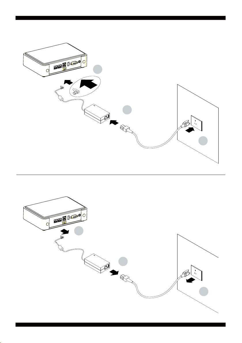
Photo 1 Insert
1
2
3
Unplug
3
2
1
3
Page 9

Chapter-1
General Information
The 3I380D is built to be an all-in-one networking control board. It’s designed to combines
all necessary input and output interfaces, which make them to be ideal control board for
thin client, fi rewall or server applications. 3I380D is the perfect platforms for whole range
of small form factor, low-power devices.
High-performance and power-efficient networking platform, the embedded motherboard
3I380D is specially designed for advanced embedded VPN or fi rewall applications where
the economical use of power is in high demand. With the sizable memory bandwidth of on
board 2GB DDR3L or DDR3L SODIMM socket or the fl exibility of expanding the memory
to 4GB DDR3L SODIMM socket, 3I380D ensures the high performance level required of
today's most popular fi rewall applications. 3I380D supports with four 10/100/1000 Mbps
Ethernet for seamless broadband connectivity. With Wake-On LAN function and the PXE
function in BIOS, these are perfect control board for networking devices. The built-in LAN
option includes four Intel I211AT LAN chipset for PCIe x 1 V2.1 interface with RJ45 for
10/100/1000 Mbps Ethernet. 3I380D also offers two COM ports (by wafer connection) to
meet the needs of COM port connectivity.
3I380D integrates PCIe mini card for mSATA & USB & SIM card interfaces. In addition,
with EHCI high-speed host controller interface; it ensures the high performance level and
also the powerful and fl exible expansion. Moreover, a single fl ash chip holds the system
BIOS, and you can change the fl ash BIOS by the Utility Update.
The 3I380D all-in-one motherboard is fully compatible with industrial standards, plus
technical enhancements and thousands of software applications developed for IBM PC/
AT compatible computers. The control logic provides high-speed performance for the most
advanced multi user and multitasking applications available today.
4
Page 10

1-1 Major Feature
1. Intel Bay Trail-I E3815 1.46GHz / Intel Bay Trail-D J1900 2.0/2.42(Burst)GHz SOC
2. Intel Bay Trail-I Integrated Graphics chipset:
Bay Trail-I E3815 Graphics speed: 400MHz
Bay Trail-D J1900 Graphics speed: 688MHz/854MHz(Turbo)
3. 1 x DDR3L SO-DIMM socket or On board DDR3L SDRAM (max. 4GB)
4. On board SSD 4/8/16/32 GB (option)
5. Support 4 x 10/100/1000 Mbps LAN on Board
(Intel I211AT LAN chipset for PCIe x 1 V2.1 interface)
6. Support 1 pair LAN Bypass function when DC Power off (option)
7. Support 1 x SATA, 7 x USB
8. Support PCIe mini cards including one for USB & SIM card interfaces,
another one for USB & mSATA interface
9. On board DC +12V Power Supply (Note: -5V, -12V no support)
10. Compact PCB Dimension: 145 x 102 mm (3.5 inch)
11. One 3G SIM card reader (for 3G mini card use)
5
Page 11

1-2 Specifi cation
1. SOC : Intel Bay Trail-I E3815 1.46GHz (Single core) /
Intel Bay Trail-D J1900 2.0/2.42(Burst)GHz (Quad core)
2. Memory : 1 x DDR3L SO-DIMM socket or On board DDR3L SDRAM (max. 4GB)
3. VGA : Intel Bay Trail-I Integrated Graphics chipset:
Bay Trail-I E3815 Graphics speed: 400MHz
Bay Trail-D J1900 Graphics speed: 688MHz/854MHz(Turbo)
4. I/O Chip : F81801U I/O chipset
5. SATA : One SATA port with independent DMA operation supported
6. NAND fl ash memory: On board SSD 4/8/16/32 GB (option)
7. LAN : 4 x Intel I211AT LAN chipset or Intel I210AT LAN chipset (option)
with 10/100/1000 Mbps for PCIe x 1 V2.1 interface
8. Serial Port : 2 x COM
9. USB : 6 x USB 2.0 (3 external + 3 internal) & 1 x USB 2.0/3.0 (internal)
10. Sound (option) : ALC886 HD Audio Specifi cation 1.0 Two channel sound
11. LAN Bypass (option) : support 100Mb LAN Bypass function when DC Power off
12. DIO (option) : Fintek F75111N chipset for 4DI/4DO
13. WDT (option): F81801U IO chipset for hardware watch dog timer support,
0~255 sec programmable
14. Expansion interface : 2 x PCIe mini card including one PCIe Mini card for
USB & SIM card interfaces, one PCIe Mini card for USB & mSATA interface
15. BIOS : Insyde UEFI BIOS
16. Dimension : 145 x 102 mm (3.5 inch)
17. Power : On board DC +12V (Note: -5V, -12V no support)
18. 3G Wireless : one 3G SIM card reader (for 3G mini card use)
6
Page 12
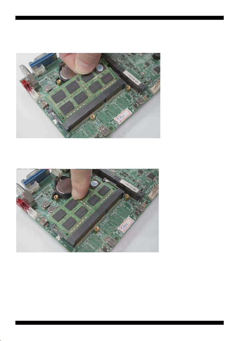
1-3 Installing the SO-DIMM (for 3I380D-D90)
1. Align the SO-DIMM with the connector at a 45 degree angle.
2. Press the SO-DIMM into the connector until you hear a click.
7
Page 13
Notices:
1.The connectors are designed to ensure the correct insertion. If you feel resistance,
check t h e connectors & golden fi nger direction, and realign the card.
2. Make sure the retaining clips (on two sides of the slot) lock onto the notches of
the card fi rmly.
8
Page 14
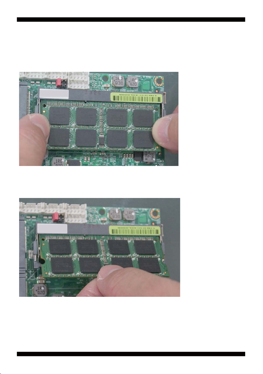
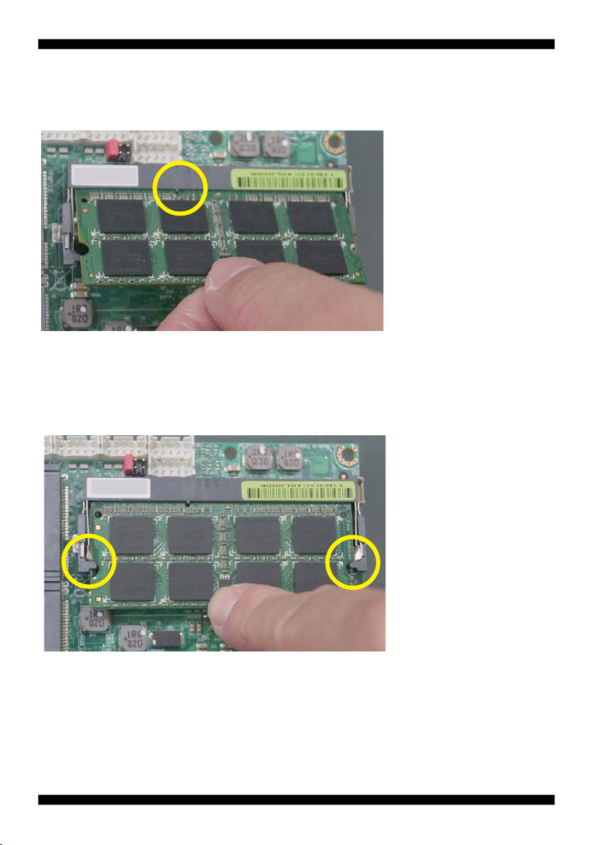
1-3-1.1 Removing the SO-DIMM (for 3I380D-D90)
1. Release the SO-DIMM by pulling outward the two retaining clips and
the SO-DIMM pops up slightly.
2. Lift the SO-DIMM out of its connector carefully.
9
Page 15
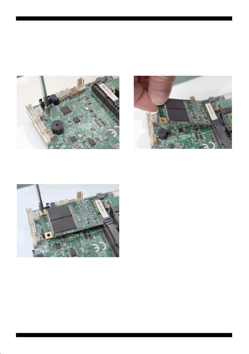
1-4 Directions for installing the Mini Card
1. Unscrew the screw on the board
3. Gently push down the Mini Card and screw the screw back.
2. Plug in the Mini Card in a 45 angle
10
Page 16

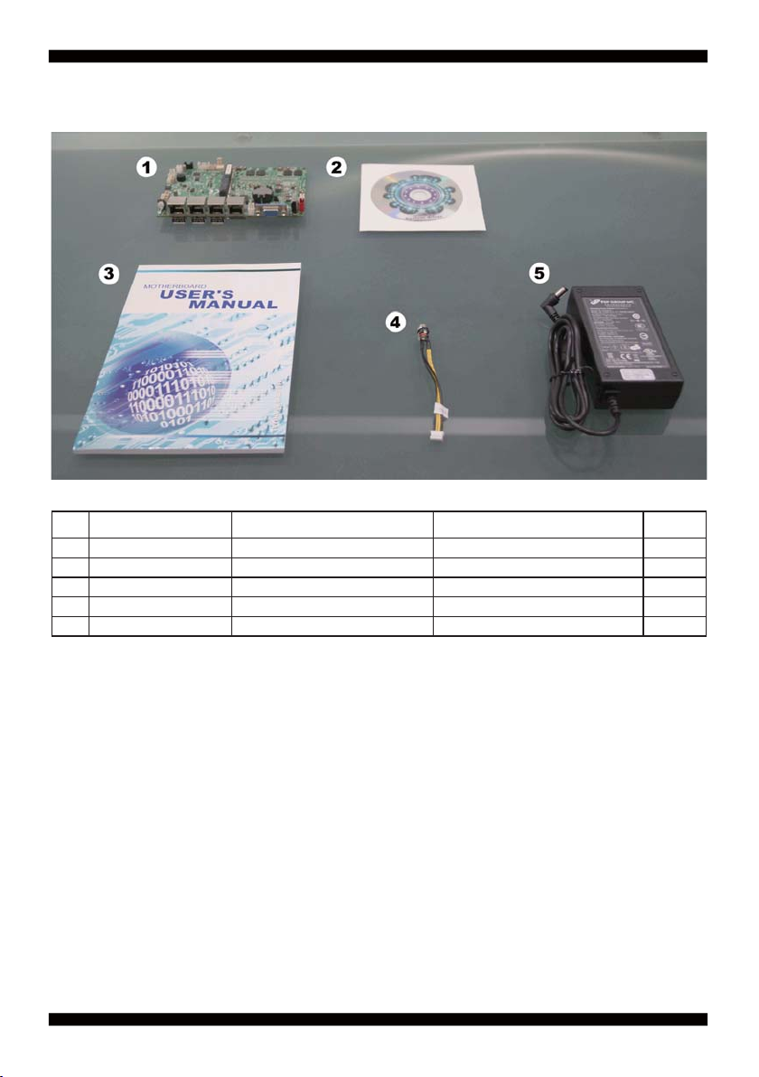
1-5 Packing List ( For 3I380D-D90)
Material Code Description Detail Specifi cation Quantit
7G1901-1481001-0 MB-3I380D-D90-00-001 LF,3I380D-D90-00,Rev.:001 1
1
6G8006-2347-0100 LEX Product Driver DVD LF, Intel Baytrail Driver 1
2
6G5212-0601-0200 60W Power Adapter,12V/5A,2.5 LF,L Type,FSP060-DBAE1,FSP 1
3
6G8001-2191-0400 Manual LF,M/B,3I380D 1
4
6G6003-7330-0100 Power Cable LF,L=9cm,2.0 1*4/DC JK 1
5
*The packing list above is for the users who purchase single motherboard. The users
who purchase the board with chassis may refer to the packing list in the Assembly Guide.
Please contact with your dealer if any of these items is missing or damaged
on delivery. And please keep all parts of the delivery package with packing
materials in case if you need to deliver or store the product in the future.
11
Page 17
1-5-1 Packing List ( For 3I380D-I12)
Material Code Description Detail Specifi cation Quantit
7G1901-1480001-0 MB-3I380D-I12-00-001 LF,3I380D-I12-00,Rev.:001 1
1
6G8006-2347-0100 LEX Product Driver DVD LF, Intel Baytrail Driver 1
2
6G5212-0601-0200 60W Power Adapter,12V/5A,2.5 LF,L Type,FSP060-DBAE1,FSP 1
3
6G8001-2191-0400 Manual LF,M/B,3I380D 1
4
6G6003-7330-0100 Power Cable LF,L=9cm,2.0 1*4/DC JK 1
5
*The packing list above is for the users who purchase single motherboard. The users
who purchase the board with chassis may refer to the packing list in the Assembly Guide.
Please contact with your dealer if any of these items is missing or damaged
on delivery. And please keep all parts of the delivery package with packing
materials in case if you need to deliver or store the product in the future.
12
Page 18

Chapter-2
Hardware Installation
2-1 Unpacking Precaution
This chapter provides the information how to install the hardware of 3I380D
Please follow section 1-5,1-5-1, 2-1 and 2-2 to check the delivery package and unpack
carefully. Please follow the jumper setting procedure.
NOTE!
1. Do not touch the board or any other sensitive components without all necessary
anti-static protection.
2. Please pay attention to the voltage limitation of DC-IN12 V 5 %.
Overuse of DC-IN voltage limitation or change to another power adapter
( not provided with this system ) will VOID warranty.
You should follow these
steps to protect the board from the static electric
discharge whenever you handle the board:
1. Ground yourself by a grounded wrist strap at all times when you
handle the 3I380D.
Well secure the ALLIGATOR clip of the strap to the end of the shielded wire lead from
a grounded object. Please put on and connect the strap before handling the
3I380D for harmlessly discharge any static electricity
through the strap.
2. Please use anti-static pad to put any components, parts, or tools on the pad whenever
you work on them outside the computer. You may also use the anti-static bag instead of
the pad. Please ask your local supplier for necessary parts on anti-static requirement.
3. Do not plug any connector or set any jumper when the power is on.
13
Page 19

2-2 Unpacking checkup
First of all, please follow all necessary steps of section 2-1 to protect 3I380D
from electricity discharge. With reference to section 1-5,1-5-1
please check the delivery package again with following steps:
1. Unpack the 3I380D board and keep all
packing material, manual and driver disc etc, do not dispose !
2. Is there any components lose or drops from the board?
DO NOT CONTINUE TO INSTALL THIS BOARD!
CONTACT THE DEALER YOU PURCHASED
THIS BOARD FROM, IMMEDIATELY.
3. Is there any visible damage on the board?
DO NOT CONTINUE TO INSTALL THIS BOARD!CONTACT
THE DEALER YOU PURCHASED THIS BOARD FROM, IMMEDIATELY.
4. Check your optional parts (i.e. DDR, CF etc.), all necessary jumpers
setting to jumper pin-set, and CMOS setup correctly.
Please also refer to all information of jumper settings in this manual.
5. Check your external devices (i.e. Add-On-Card, Driver Type etc.)
for complete add-in or connection and CMOS setup correctly.
Please also refer to all information of connector connection in this manual.
6. Please keep all necessary manual and driver disc in a good condition for future
re-installation if you change your Operating System.
14
Page 20
2-3 Dimension-3I380D
0
3.07
36.38
66.6
89.71
97.49
98.32
102
146
137.18
83.82
35.43
2.99
0
Ŗ6
0
Ŗ
3.4
03
04
03
03
04
05
27.81
04
05
26.66
146
03
142
03
04
130.85
137.18
03
03
04
111.79
04
05
92.73
03
04
05
73.67
03
04
05
8.1
100.89
2.99
0
94.39
94.81
102
03
6.5
SIM CARD
117
15
Page 21
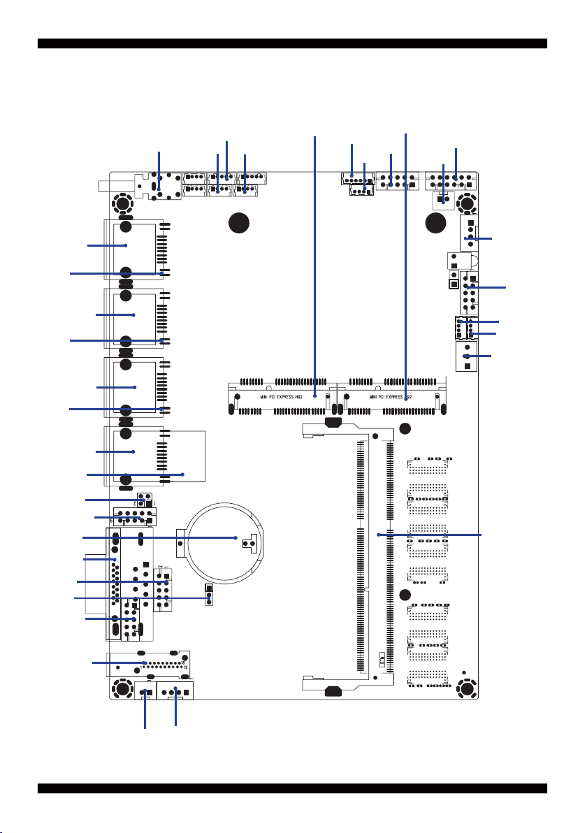
2-4 Layout-3I380D
CU3
(Bottom side)
CL4
CU2
(Bottom side)
CL3
CU1
(Bottom side)
CL2
CL1
SIM1
(Bottom side)
JSC2
CC2
BAT1
CG1
CG11
JSB1
CC11
SWP1
CU43
CU5
CU44
MPCE1
CKM1
CO1
MPCE2
CIO1
SWP2
CFP1
CPO1
CA1
CU41
CU42
FAN1
SODIMM1
(FOR 3I380D-D90)
HDMI1
CPI2
CPI1
16
Page 22
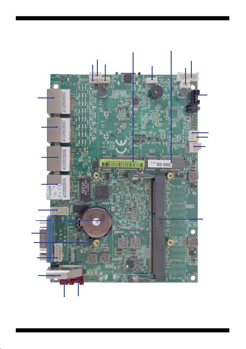
2-5 Diagram- 3I380D-D90
CL4
CC2
BAT1
CL3
CL2
CL1
CU43
CU5
CU44
MPCE1
CO1
MPCE2
CFP1
SWP2
CPO1
CU41
CU42
FAN1
SODIMM1
CG1
JSB1
CC11
HDMI1
CPI2
CPI1
17
Page 23
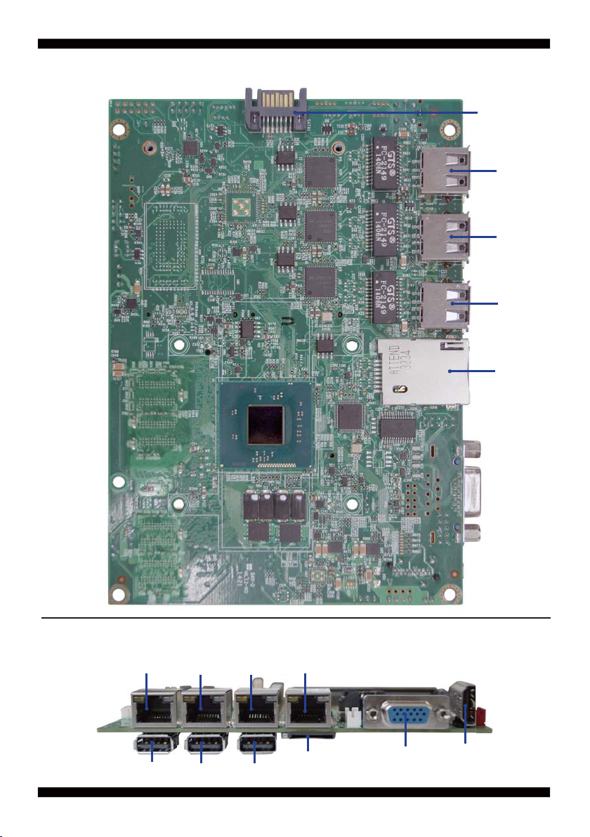
2-5-1 Bottom Side Diagram- 3I380D-D90
SATA 1
CU3
CU2
CU1
SIM1
BACK Panel-3I380D-D90
LAN4
USB
LAN3
USB
LAN2
USB
LAN1
SIM
18
VGA
HDMI
Page 24
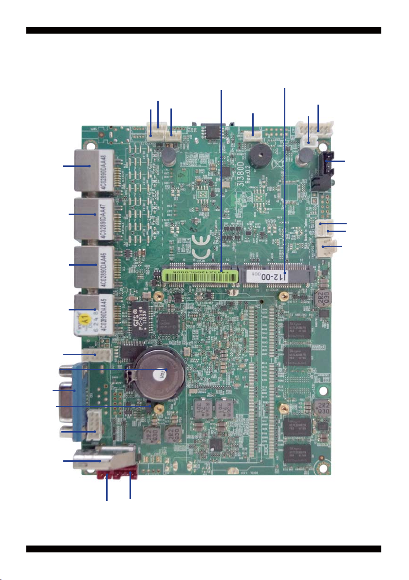
2-5-2 Diagram- 3I380D-I12
CL4
CC2
BAT1
CL3
CL2
CL1
CU43
CU5
CU44
MPCE1
CO1
MPCE2
CFP1
SWP2
CPO1
CU41
CU42
FAN1
CG1
JSB1
CC11
HDMI1
CPI2
CPI1
19
Page 25
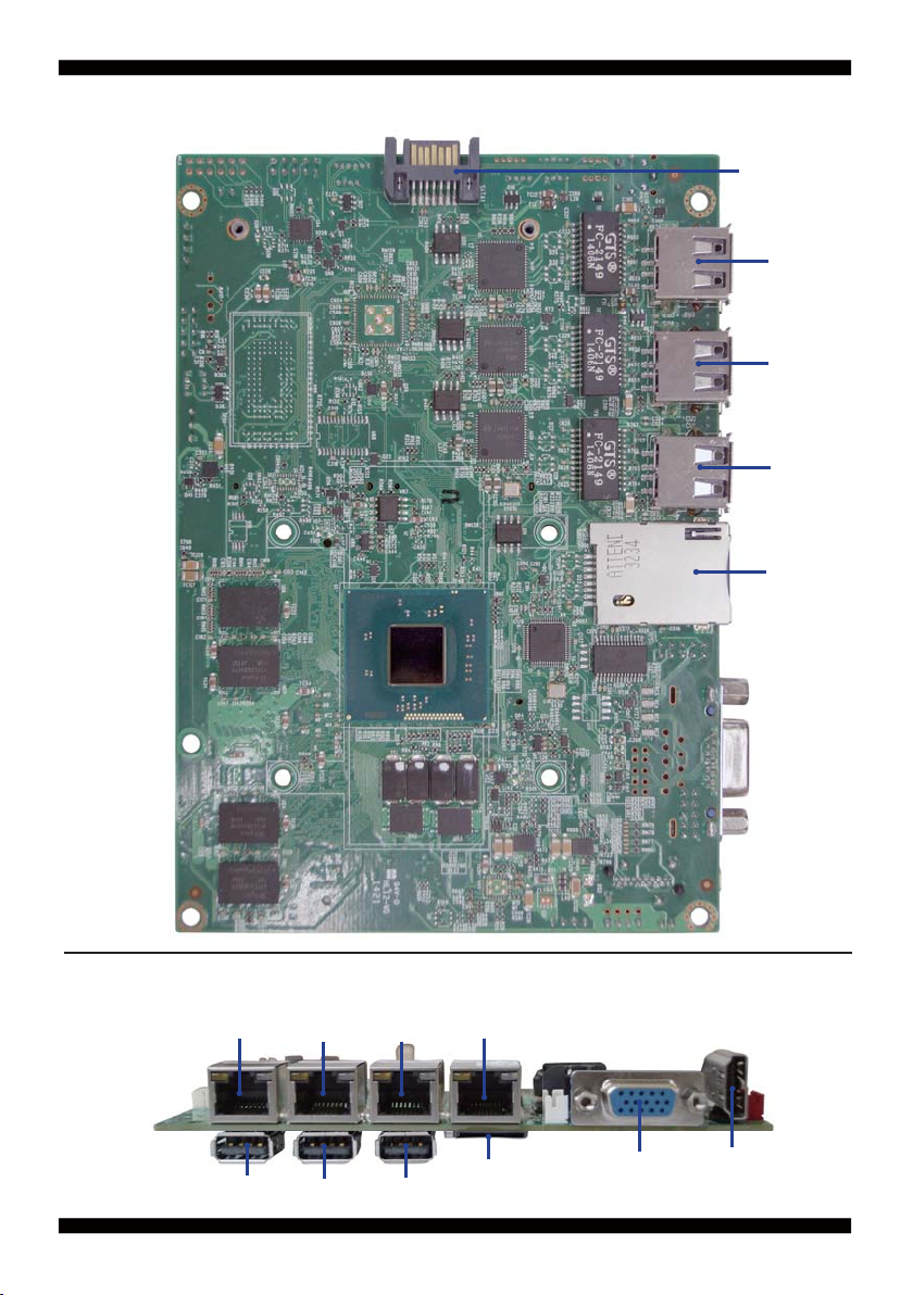
2-5-3 Bottom Side Diagram- 3I380D-I12
SATA 1
CU3
CU2
CU1
SIM1
BACK Panel-3I380D-I12
LAN4
USB
LAN3
USB
LAN2
USB
20
LAN1
SIM
VGA
HDMI
Page 26

2-6 Install Memory
This motherboard provides one 204-pin Small Outline Dual In-line Memory Module (SODIMM)
socket for memory expansion available maximum to of 2GB/4GB/8GB DDR3L SDRAM.
DDR3L clock supports: DDR3 1333/1066MT/S
Valid Memory Confi gurations
Total Memory
DIMM1
System Accept or Not
Max.
DS/SS Accept
8GB
SS: Single Sided DIMMDS: Double Sided DIMM
NOTE!
The detected memory size is less than actual installed memory size since
some memory has been allocated for system use.
That’s how PC works with system memory.
Please refer to page 7 for installation of memory module.
21
Page 27
2-7 List of Jumpers
JSB1: CMOS clear select
JSC2: COM2 RS422/RS485 select (Option)
2-8 Jumper Setting Description
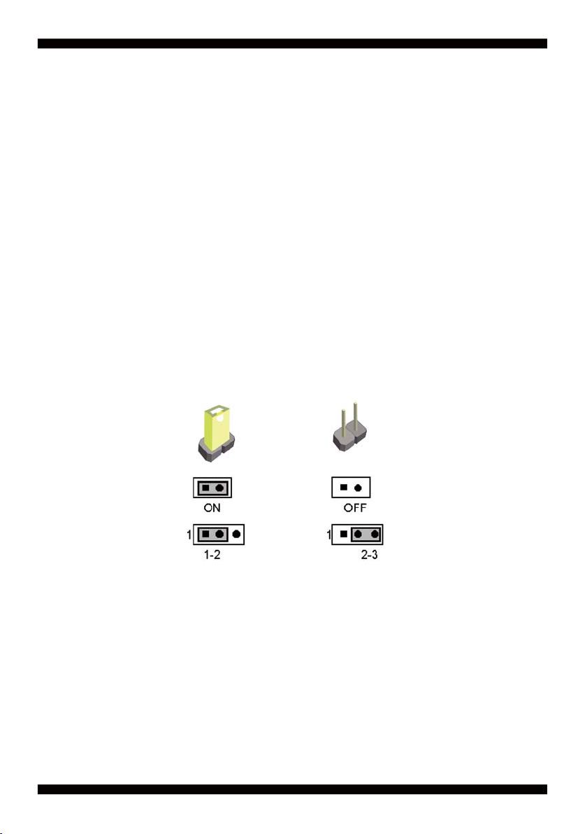
A jumper is ON as a closed circuit with a plastic cap covering two pins. A jumper is OFF
as an open circuit without the plastic cap. Some jumpers have three pins, labeled 1, 2,
and 3. You could connect either pin 1 and 2 or 2 and 3.The below fi gure 2.2 shows the
examples of different jumper settings in this manual.
Figure 2.2
All jumpers already have its default setting with the plastic cap inserted as ON,
or without the plastic cap as OFF. The default setting may be referred in this
manual with a " * " symbol .
22
Page 28
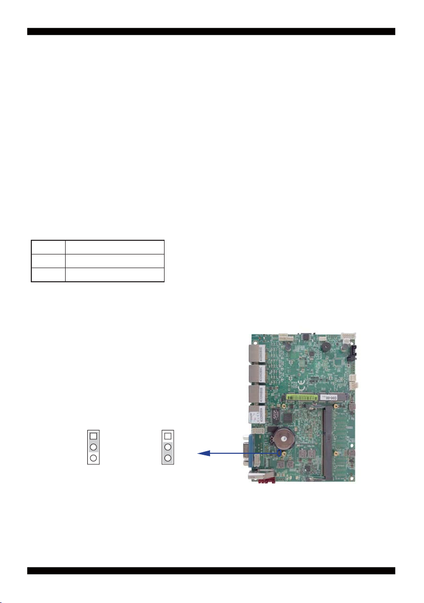
2-9 CMOS Data Clear
A battery must be used to retain the motherboard confi guration in CMOS RAM.
Close Pin1 and pin 2 of JSB1 to store the CMOS data.
To clear the CMOS,follow the procedures below:
1. Turn off the system and unplug teh AC power
2. Remove DC 12V power cable from DC 12V power connector
3. Locate JSB1 and close pin 1-2 for few seconds
4. Return to default setting by close pin 1-2
5. Connect DC 12V power cable back to DC 12V Power connector
JSB1: CMOS Data Clear
JSB1 Description
1-2 Normal set
2-3 CMOS data clear
Note: Normal work is open jumper
JSB1
*Normal Clear Setting
Note: Do not clear CMOS unless
1. Troubleshooting
2. Forget password
3. You fail over-clocking system
11
22
33
23
Page 29
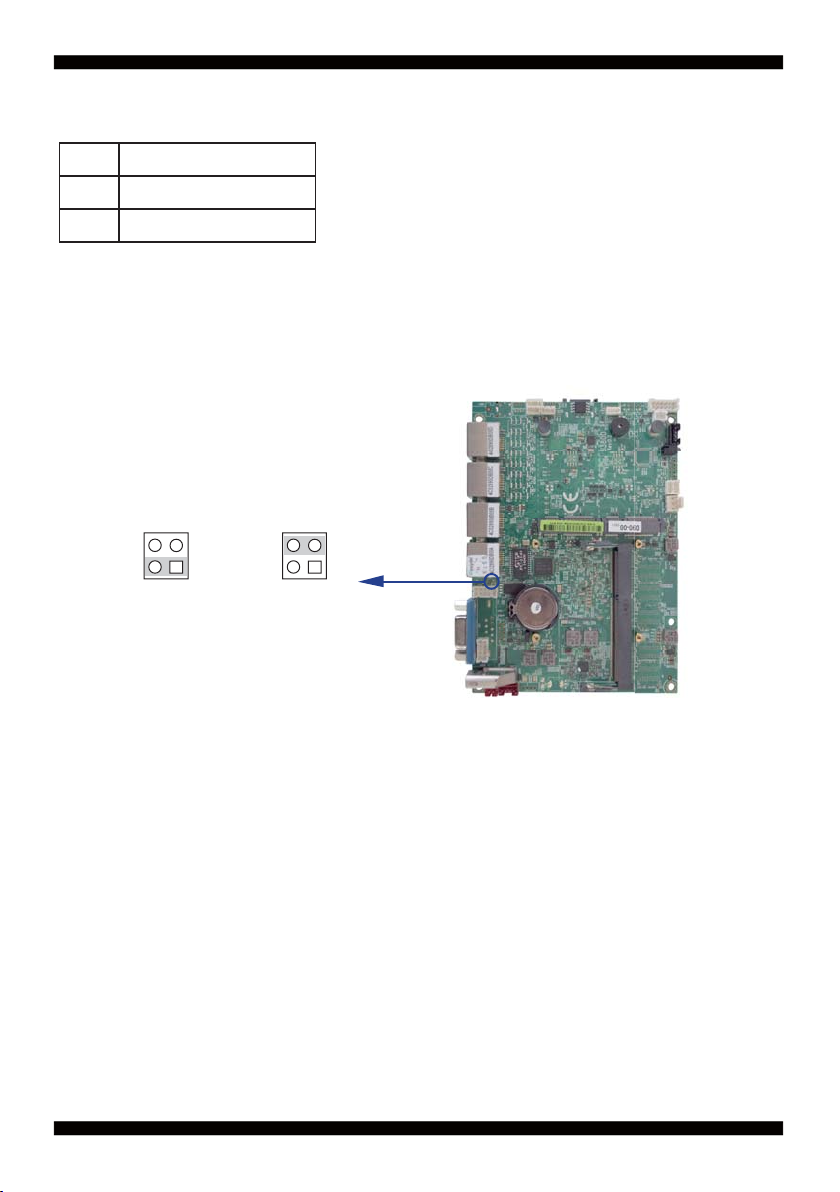
2-10 JSC2:COM2 RS422/RS485 select (Option)
JSC2 Description
RS422
*1-2
RS485
3-4
Note: RS422/485 setting by both H/W jumper and
BIOS CMOS setting
JSC2
44
22
*Normal RS485
33
11
24
Page 30

Chapter-3
Connection
This chapter provides all necessary information of the peripheral's connections,
switches and indicators. Always power off the board before you install the peripherals.
3-1 List of Connectors
CPI1: DC-in 1x4pin(2.0mm) Red wafer connector
DC-in 1x2 pin(2.0mm) Red wafer connector
CPI2
:
DC-in 2x4 pin(2.0mm) wafer connector (Option)
CPI11
:
Li 3V battery holder
BAT1
:
DC +5/+12V output 1x4 pin(2.0mm) Black wafer connector
CPO1
:
Front panel port 2x6 pin(2.00mm) wafer for LED
CFP1
:
Power Button /Power LED(Blue) (Option)
SWP1
:
Power Button 1x2 pin(2.0mm) wafer
SWP2
:
CPU fan 1x3 pin(2.54mm) wafer
FAN1
:
DSUB VGA connector
CG1
:
DSUB VGA wafer connector (Option)
CG11
:
HDMI1
CA1
CC1
CC11
CC2
CIO1
CO1
CKM1
CL1/CL2/CL3/CL4
CL11/CL21/CL31/CL41
CL32/CL42
CU1/CU2/CU3
CU41
CU42
CU5
CU43/CU44
SATA1
MPCE1/MPCE2
SIM1
MSD1
SODIM1
HDMI Type A 90° connector
:
Mic-in/Line out/Line in 2x5 pin(2.0mm) wafer connector (Option)
:
DB9 COM1 connector (Option)
:
COM1 2x5pin(2.0mm) wafer
:
COM2 2x5pin(2.0mm) wafer
:
DI port 0 ~ 3, DO port 0 ~ 3 2x5 pin (2.0mm) wafer (Option)
:
2
I C 4pin (1.25mm) wafer
:
KB/MS port 1x6 pin (1.25mm) wafer connector (Option)
:
LAN RJ45 connector
:
LAN3/4 port 2x4 pin(2.0mm) wafer connector (Option)
:
LAN3/4 LED port 1x4 pin(1.25mm) wafer connector (Option)
:
USB port 1/2/3 Type A connector
:
USB2.0 port 4pin(1.25mm) wafer (share with MPCE1 USB signal)
:
USB2.0 port 4pin(1.25mm) wafer (share with MPCE2 USB signal)
:
USB3.0 port 5pin(1.25mm)wafer (For CU001 use)
:
USB2.0 port 4pin(1.25mm) wafer
:
SATA port 0 (Gen III) connectors 7pin
:
Mini card port 1/2 sockets 52pin
:
SIM port 1 card socket(push-push)
:
MicroSD port socket(push-push) (Option)
:
SO-DIM DDR3L 1.35V DRAM Socket
:
25
Page 31

3-2 DC power input
CPI1: DC-IN Internal Connector (1x4pin 2.0mm Red wafer)
PIN NO. Description PIN NO. Description
1 GND 2 +VAD_AC
3 +VAD_AC 4 GND
Note: 1. DC in from adapter plug in
CPI2: DC-IN Internal Connector (1x2 pin 2.0mm Red Wafer)
PIN NO. Description
1 +VAD_AC
2 GND
Note: DC in from adapter plug in
CPI11: DC-IN Internal Connector (2x4 pin 2.0mm Wafer )(Option)
PIN NO. Description PIN NO. Description
1 GND 2 GND
3 +VAD_AC 4 +VAD_AC
5 +VAD_AC 6 +VAD_AC
7 GND 8 GND
Note: 1. DC in from adapter plug in
2. Share with CPI1 Connector
CPI2
pin1
pin1
CPI1
26
Page 32
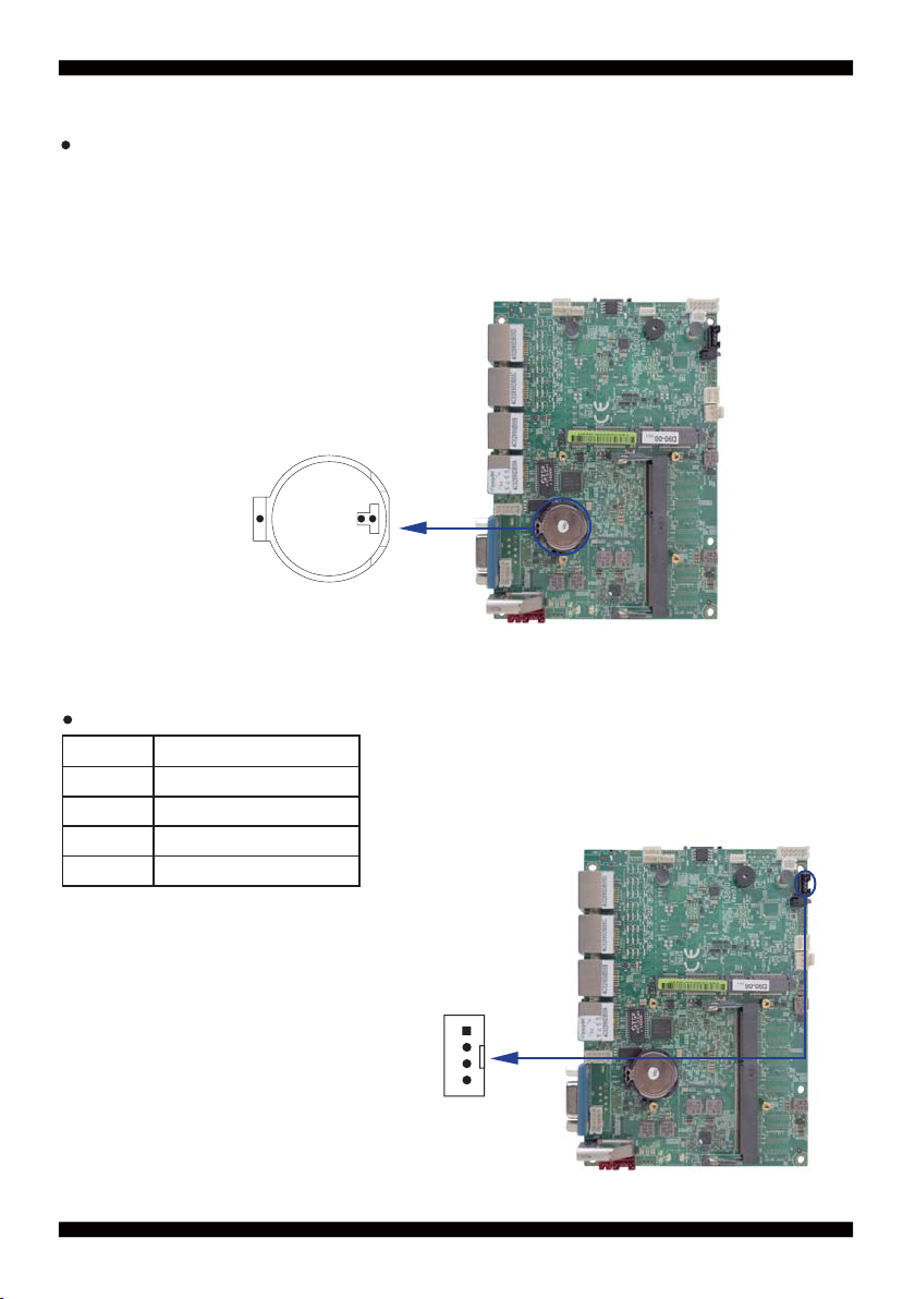
3-3 Battery Input
BAT1: 3V Battery hold 2pin
BAT1: Battery use Li 3V / 220mAh (CR2032)
Note: 1. When board without Adaptor plug in,this board power RTC
consumption about 2.7uA
2. If adaptor always plug in RTC power consumption about 0.1uA
BAT1
3-4 DC Power output
CPO1: +12V/+5V DC voltage output (1x4pin 2.00mm Black wafer)
PIN NO. Description
1 +5V
2 GND
3 GND
4 +12V*
Note: DC in +12V by switch to DC-out voltage +12V,
so DC in need stable +12V input
CPO1
27
pin1
Page 33

3-5 Front panel & FAN
CFP1 Front panel LED connector (2x6pin 2.00mm wafer)
PIN NO. Description PIN NO. Description
2 GND 1 Power LED+
4 GND 3 HDD LED+
6 LAN1 LED- 5 LAN1 LED+
8 LAN2 LED- 7 LAN2 LED+
10 LAN3 LED- 9 LAN3 LED+
12 LAN4 LED- 11 LAN4 LED+
Note: pin3 can OEM BOM set to reset pin
SWP2 Power button connector (1x2pin 2.0mm wafer)
PIN NO. Description
1 Power button pin
2 Power button GND
FAN1: CPU FAN connector (1x3pin 2.54mm wafer)
PIN NO. Description
1 GND
2 +12V
3 FAN speed detect
Note: DC in +12V by switch to FAN power +12V,
so DC in need stable +12V input
28
pin1
10
FAN1
CFP1
pin1
SWP2
pin1
Page 34

3-6 Display interface
CG1: DSUB VGA connector (DB15 pin)
PIN NO. Description PIN NO. Description PIN NO. Description
1 RED 6 GND 11 NC
2 GREEN 7 GND 12 DDC DATA
3 BLUE 8 GND 13 H-SYNC
4 NC 9 NC 14 V-SYNC
5 GND 10 GND 15 DDC CLOCK
CG11: VGA wafer connector (2x5pin 2.0mm wafer) (Option)
PIN NO. Description PIN NO. Description
1 BLUE 2 GND
3 GND 4 DDC CLOCK
5 GREEN 6 V-SYNC
7 GND 8 H-SYNC
9 RED 10 DDC DATA
HDMI1: HDMI Connector (Type A)
PIN NO. Description PIN NO. Description
1 TMDS DATA2+ 2 GND
3 TMDS DATA2- 4 TMDS DATA1+
5 GND 6 TMDS DATA1-
7 TMDS DATA0+ 8 GND
9 TMDS DATA0- 10 TMDS CLK+
11 GND 12 TMDS CLK-
13 NC 14 NC
15 DDC CLK 16 DDC DATA
17 GND 18 +5V
19 H.P. Detect
*Note: HDMI support 1.3a Spec
10
CG1
pin1
CG11
HDMI1
29
Page 35

3-7 Audio interface (option)
CA1: Mic in/Line in/Line out wafer connector (2x5pin 2.00mm wafer)
PIN NO. Description PIN NO. Description
1 LINEOUT_R 2 MIC_IN
3 LINE_IN_R 4 GND
5 GND 6 SPDIF_O
7 LINE_IN_L 8 +5V
9 LINEOUT_L 10 MIC_IN
CA1
pin1
10
CC2
10
pin1
3-8 I/O Interface
COM ports (COM1~COM6 from super I/O)
COM1/2 default support RS232 mode
CC1 share with CC11 wafer connector
RS232 mode ports (2x5pin 2.0mm Wafer)
CC1: COM1 DB9 CC11: COM1 wafer connector
CC2: COM2 wafer connector
PIN NO. Description PIN NO. Description
1 DCD 2 RXD
3 TXD 4 DTR
5 GND 6 DSR
7 RTS 8 CTS
9 RI 10 +5V
Note: 1. CC1 & CC11 wafer connector RS232 function for OEM BOM request
pin1
10
CC11
30
Page 36

RS485 mode ports (2x5pin 2.0mm wafer)
CC1: COM1 DB9 CC11: COM1 wafer connector
CC2: COM2 wafer connector
PIN NO. Description PIN NO. Description
1 RS485 TX- 2 RS485 TX+
3NC 4NC
5 GND 6 NC
7NC 8NC
9 NC 10 +5V
Note: 1. CC1 & CC11 wafer connector RS485 function for OEM BOM request
2. BIOS need setting to RS485 mode
RS422 mode ports (2x5pin 2.0mm wafer)
CC1: COM1 DB9 CC11: COM1 wafer connector
CC2: COM2 wafer connector
PIN NO. Description PIN NO. Description
1 RS422 TX- 2 RS422 TX+
3 RS422 RX+ 4 RS422 RX
5 GND 6 NC
7NC 8NC
9 NC 10 +5V
Note: 1. CC1 & CC11 wafer connector RS422 function for OEM BOM request
2. BIOS need setting to RS422 mode
31
Page 37

3-9 Digital Input / Output (option)
CIO1 DIO 0 ~ 3 (2x5pin 2.0mm wafer)
PIN NO. Description PIN NO. Description
1 DI-0 2 DO-3
3 DI-1 4 DO-2
5 DI-2 6 DO-1
7 DI-3 8 DO-0
9 GND 10 +5V
Note: 1. DI pin default pull up 10KΩ to +5V
2. If use need isolate circuit to control external device
3. F75111N-1 I C bus address 0x9c
For F75111N I C DIO device:
DC spec:
Input low Voltage (VIL): +0.8 Max
Input High Voltage (VIH): +2V Min
Output low Current (IOL): 10mA (Min) VOL=0.4V
Output High Current (IOH): -10mA (Min) VOH=2.4V
Hardware watch Dog Timer support use F81801U
Watch Dog Time value 0~255sec
The system will be issued reset. When WDT is enable the hardware start down counter to zero.
The reset timer have 10~20% tolerance upon the Temperature.
Note: If want to SDK support. Please contact to sales window.
Please refer to page 87 for APPENDIX C: F75111N I C DIO DECICE
2
10
CIO1
2
2
pin1
32
Page 38

2
3-10 I C Bus Interface
2
CO1: I C (SM) bus connector (1x4pin 1.25mm wafer)
PIN NO. 1 2 3 4
Description +3.3V GND SMB_CLK SMB_DATA
3-11 PS2 KB/MS (option)
CKM1: KB/MS port (1x6pin 1.25mm wafer)
PIN NO. 1 2 3 4 5 6
Description +5V KB/DAT KB/CLK GND MS/DAT MS/CLK
CKM1
pin1
CO1
pin1
3-12 LAN Interface
CL1 / CL2 / CL3 / CL4: LAN Giga/100Mb (RJ45 Jack)
PIN NO. Description PIN NO. Description
1 TD0-/TX+ 5 TD2-/NC
2 TD0+/TX- 6 TD2+/RX-
3 TD1-/RX+ 7 TD3-/NC
4 TD1+/NC 8 TD3+/NC
RJ45 LAN Connector--- LED defi ne Giga/100MB Connector
SPEED 10 Mbps 100 Mbps 1000 Mbps
Indicate
Side
LED
Back Back Back
Link Link Link
ACT ACT ACT
Orange Orange Orange
Front Front Front
ACT ACT ACT
Orange Green Orange OrangeLAN Light
Red
CL1CL3 CL2CL4
33
Page 39

CL11/CL21/CL31/CL41: LAN port Giga /100Mb( 2x4pin 2.0mm wafer) (Option)
)
PIN NO. Description PIN NO. Description
1 TD0-/TX+ 2 TD2-/NC
3 TD0+/TX- 4 TD2+/RX-
5 TD1-/RX+ 6 TD3-/NC
7 TD1+/NC 8 TD3+/NC
CL32/CL44 : LAN LED wafer (1x4pin 1.25mm wafer) (Option)
PIN NO. 1 2 3 4
Description +3.3V Speed 10M Speed 100M Speed 1000M
3-13 USB Interface
CU1 / CU2 / CU3: USB1/2/3 ports ( USB Type A connector )
PIN NO. Description
1 +5V
2 USB DATA -
3 USB DATA +
4 GND
Note: 1. Attention ! Check Device Power in spec
CU41 / CU42: Internal USB ports (1x4pin 1.25mm wafer)
PIN NO. Description
1 +5V
2 USB DATA -
3 USB DATA +
4 GND
Note: 1. Attention ! Check Device Power in spec
2. CU41 share Mini card1 USB signal.
3. CU42 share Mini card2 USB signal.
er
CU41 CU42
pin1
CU1CU3 CU2
34
Page 40

CU5: USB3.0 only port (1x5pin 1.25mm wafer) (For CU001 use)
PIN NO. Description
1 USB3_TX+
2 USB3_TX-
3 GND
4 USB3_RX+
5 USB3_RX-
Note: 1. If use CU5 must to use CU43 (4pin 1.25mm Wafer)
CU43 / CU44: Internal USB ports (1x4pin 1.25mm wafer)
PIN NO. Description
1 +5V
2 USB DATA -
3 USB DATA +
4 GND
CU5
pin1
pin1
CU43 CU44
35
Page 41

3-14 SATA interface
SATA1: SATA1 connector
PIN NO. Description
1 GND
2 DATA TX +
3 D ATA TX-
4 GND
5 DATA RX-
6 DATA RX+
7 GND
Note: 1. SATA1 support SATA 2.0 spec update 3Gb/sec.
2. CPO1 provide SATA HDD power +12V, GND, +5V
SSD use SATA port 2 channel
Note: 1. On board SSD for OEM option
SATA 1
SSD
3-15 MicroSD Card interface (Socket Push-Push) (Option)
PIN NO. Description PIN NO. Description
1 SDMMC3_D2 2 SDMMC3_D3
3 SDMMC3_CMD 4 +VSDIO
5 SDMMC3_CLK 6 GND
7 SDMMC3_D0 8 SDMMC3_D1
9 SDMMC3_CD_N 10 GND
Note: 1. MicroSD card for OEM option
2.Use only in WIN8
36
Page 42

3-16 Module socket
Mini card & SIM card
MPCE1/MPCE2: Support USB and PCIe x1 Interface (Mini card socket 52pin)
PIN NO. Description PIN NO. Description
1 NC 2 +3.3V
3 NC 4 GND
5 NC 6 +1.5V
7 NC 8 SIM Power
9 GND 10 SIM Data
11 PCIe-CLK- 12 SIM CLK
13 PCIe-CLK+ 14 SIM Reset
15 GND 16 SIM RFU
KEY KEY KEY KEY
17 NC 18 GND
19 NC 20 NC
21 GND 22 RST-
23 PCIe-RX-/mSATA-RX+ 24 +3.3V
25 PCIe-RX+/mSATA-RX- 26 GND
27 GND 28 +1.5V
29 GND 30 SMB-CLK
31 PCIe-TX-/mSATA-TX- 32 SMB-DATA
33 PCIe-TX+/mSATA-TX+ 34 GND
35 GND 36 USB-DATA-
37 GND 38 USB-DATA+
39 +3.3V 40 GND
41 +3.3V 42 NC
43 NC 44 NC
45 NC 46 NC
47 NC 48 +1.5V
49 NC 50 GND
51 mSATA-Detect 52 +3.3V
pin1 pin1
MPCE1
Note: 1. MPCE1 used SOC-USB port 1(share with CU41)
2. MPCE1 used PCIe port 4(share with CL4(LAN4))
3. MPCE2 used HUB-USB port 3(share with CU42)
4. MPCE1 Pin 8, 10,12,14,16 for SIM1 card reader use.
5. Just only MPCE2 pin23, 25, 31, 33 supported mSATA device
6. mSATA use system SATA port 2
pin52
pin52
MPCE2
37
Page 43

3-17 SIM Socket
SIM1: SIM card socket pin defi ne is follow ISO 7816-2 smart card standard
PIN NO. Description PIN NO. Description
1 VCC 1 GND
2 RST 2 VPP
3 CLK 3 DATA
4 RUF 4 GND
Note: 1. MPCE1 Pin 8, 10,12,14,16 for SIM1 card reader use.
SIM1
3-18 SODIMM socket (Option)
Note: SODIM1: SO-DIMM DDR3L 1.35V DRAM Socket
38
SODIMM1
(only 3I380D-D90)
Page 44

3-19 Connector wafer of Compatible Brand and part number list
Location CKTS PITCH Brand Name Mating connector Cable housing
CA1 2x5 10Pin 2.0mm JST B10B-PHDSS PHDR-10VS
CG11 2x5 10Pin 2.0mm JST B10B-PHDSS PHDR-10VS
CC11 2x5 10Pin 2.0mm JST B10B-PHDSS PHDR-10VS
CC2 2x5 10Pin 2.0mm JST B10B-PHDSS PHDR-10VS
CFP1 2x6 12Pin 2.0mm JST B12B-PHDSS PHDR-12VS
CIO1 2x5 10Pin 2.0mm JST B10B-PHDSS PHDR-10VS
CL31 2x4 8Pin 2.0mm JST B8B-PHDSS PHDR-08VS
CL41 2x4 8Pin 2.0mm JST B8B-PHDSS PHDR-08VS
CL32 1x4 4Pin 1.25mm MOLEX 53047-0410 51021-0400
CL44 1x4 4Pin 1.25mm MOLEX 53047-0410 51021-0400
CO1 1x4 4Pin 1.25mm MOLEX 53047-0410 51021-0400
CPI1 1x4 4Pin 2.0mm JST B4B-PH-KL PHR-4
CPI2 1x2 2Pin 2.0mm JST B2B-PH-KL PHR-2
CPI11 2x4 8Pin 2.0mm JST B8B-PHDSS PHDR-08VS
CPO1 1x4 4Pin 2.0mm JST B4B-PH-KL PHR-4
SWP2 1x2 2Pin 2.0mm JST B2B-PH-KL PHR-2
FAN1 1x3 3Pin 2.54mm MOLEX 7879-3 7880-3
CKM1 1x6 6Pin 1.25mm MOLEX 53047-0610 51021-0600
CU41 1x4 4Pin 1.25mm MOLEX 53047-0410 51021-0400
CU42 1x4 4Pin 1.25mm MOLEX 53047-0410 51021-0400
CU43 1x4 4Pin 1.25mm MOLEX 53047-0410 51021-0400
CU44 1x4 4Pin 1.25mm MOLEX 53047-0410 51021-0400
CU5 1x5 5Pin 1.25mm MOLEX 53047-0510 51021-0500
39
Page 45

Chapter-4
Introduction of BIOS
The BIOS is a program located in the Flash Memory on the motherboard.
This program is a bridge between motherboard and operating system.
When you start the computer, the BIOS program gains control.
The BIOS fi rst operates an auto-diagnostic test called POST (Power on Self Test) for
all the necessary hardware, it detects the entire hardware devices and confi gures
the parameters of the hardware synchronization. After these tasks are completed,
BIOS will give control of the computer back to operating system (OS).
Since the BIOS is the only channel for
hardware and software to communicate with, it is the key factor of system stability and of
ensuring your system performance at best.
In the BIOS Setup main menu, you can see several options. We will explain these options
in the following pages. First, let us see the function keys you may use here:
Press <Esc> to quit the BIOS Setup.
Press ↑↓←→(up, down, left, right) to choose the option you want to confi rm or modify.
Press <F10> to save these parameters and to exit the
BIOS Setup menu after you complete the setup of BIOS parameters.
Press Page Up/Page Down or +/- keys to modify the
BIOS parameters for the active option.
4-1 Enter Setup
Power on the computer and press <Del> key immediately to enter Setup.
If the message disappears before your respond but you still wish to enter Setup,
restart the system by turning it OFF then ON or pressing the "RESET" button on the
system case. You may also restart the system by simultaneously pressing <Ctrl>,
<Alt> and <Delete> keys.
40
Page 46

4-2 BIOS Menu Screen & Function Keys
In the above BIOS Setup main menu of, you can see several options.
We will explain these options step by step in the following pages of this
chapter, but let us fi rst see a short description of the function keys you may use here:
Press ←→ (left, right) to select screen;
●
Press ↑↓ (up, down) to choose, in the main menu, the option you want to confi rm or to modify.
●
Press <Enter> to select.
●
Press <+>/<–> or <F5>/<F6> keys when you want to modify the BIOS parameters for
●
the active option.
[F1]: General help.
●
[F9]: Optimized defaults.
●
[F10]: Save & Exit.
●
Press <Esc> to quit the BIOS Setup.
●
41
Page 47

4-3 General Help
Status Page Setup Menu/ Option Page Setup Menu
Press F1 to pop up a help window that describes the appropriate keys to use and the possible
selections for the highlighted item. To exit the Help Window, press <Esc>
4-4 Menu Bars
There are six menu bars on top of BIOS screen:
Main To change system basic confi guration
Advanced To change system advanced confi guration
Security Password settings
Power PME & Power button settings
Boot Exit Save setting, loading and exit options.
User can press the right or left arrow key on the keyboard to switch from menu bar.
The selected one is highlighted.
42
Page 48

4-5 Main
Main menu screen includes some basic system information. Highlight the item and then use
the <+> or <-> and numerical keyboard keys to select the value you want in each item.
System Date
Set the Date. Please use [Tab] to switch between data elements.
System Time
Set the Time. Please use [Tab] to switch between data elements.
43
Page 49

4-6 Advanced
Boot Confi guration
Please refer section 4-6-1
PCI Express Confi guration
Please refer section 4-6-2
USB Confi guration
Please refer section 4-6-3
Video Confi guration
Please refer section 4-6-4
Thermal Confi guration
Please refer section 4-6-5
SATA Confi guration
Please refer section 4-6-6
Console Redirection
Please refer section 4-6-7
ACPI Table/Fetures Control
Please refer section 4-6-8
44
Page 50

4-6-1 Boot Confi guration
Numlock
Select Power-on state for Numlock, default is <ON>
45
Page 51

4-6-2 PCI Express Confi guration
PCIe 1/2/3/4 confi guration settings
46
Page 52

4-6-2-1 ► PCI Express Root Port 1/2/3/4
Control the PCI Express Root Port.
The optional settings are: Enabled(default), Disabled.
47
Page 53

4-6-2-2 ►PCIE Port 1/2/3/4 Speed
Select PCI Express port speed.
The optional settings are: Gen1(default), Gen2
48
Page 54
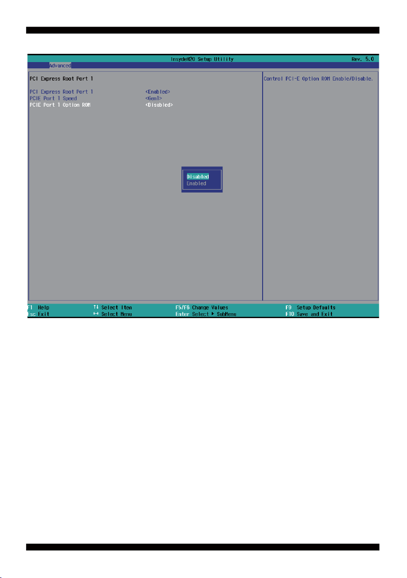
4-6-2-3 ►PCIE Port 1/2/3/4 Option ROM
Select PCIE TXE ROM support
The optional settings are: Disabled(default), Enabled
49
Page 55
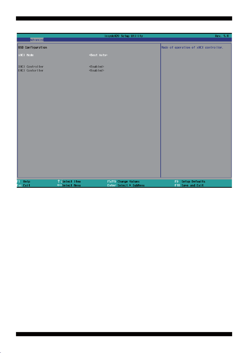
4-6-3 USB Confi guration
XHCI Mode
Mode of operation of xHCI controller.
The optional settings are: Best Auto(default), Enabled, Disabled.
50
Page 56

4-6-4 Video Confi guration
Logo & SCU Resolution 1024 x 768(Default) , 800 x 600 , 640 x480
51
Page 57

PAVC
The function is setting the display quality,
The optional settings are: Disabled, LITE Mode(default), SERPENT Mode
Aperture Size
The optional settings are: 128MB, 256MB(default), 512MB.
IGD - DVMT Pre-Allocated
Use this item to select DVMT 5.0 pre-allocated (fi xed) graphics memory size used by the
internal graphics device.
The optional settings are:
64(default)/96/128/160/192/224/256/288/320/352/384/416/448/480/512MB
IGD - DVMT Total Gfx Mem
Use this item to select DVMT 5.0 total graphics memory size used by the
internal graphics device.
The optional settings are:128M, 256M(default), MAX
52
Page 58

4-6-5 Thermal Confi guration
Thermal Confi guration Parameters
This Value controls the temperature of the ACPI Critical Trip Point, the point in which the OS will
shutdown the system.
Critical Trip point is the shutdown temperature, the default value is 110˚
The CPU frequency will auto reduce when cpu temperature arrived to passive Trip point.
The default of the passive trip point is 105˚
Note : For BIOS 3I380DDX.ROM
Critical Trip point is the shutdown temperature, the default value is 105˚
The CPU frequency will auto reduce when cpu temperature arrived to passive Trip point.
The default of the passive trip point is 100˚
53
Page 59

4-6-6 SATA Confi guration
SATA Controller
Use this item to Enable or Disable SATA Device.
The optional settings are: Enabled(default) or Disabled
Chipset SATA Mode
Determine how SATA controller(s) operate.
The optional settings are: IDE Mode(default), AHCI Mode.
SATA Speed
Indicates the maximum speed the SATA controller can support.
The optional settings: Gen1, Gen2(default).
IDE Mode
Legacy IDE or Native IDE MODE,
The optional settings: Legacy IDE or Native IDE(default)
SATA Port 0 Connected to an ODD
Use this item to Enable or Disable SATA Port0 ODD function
The optional settings are: Enabled(default) or Disable
54
Page 60

SATA Port 1 Connected to an ODD
Use this item to Enable or Disable SATA Port1 ODD function
The optional settings are: Enabled(default) or Disable
4-6-7 Console Redirection
Console Serial Redirect
Use this item to enable or disable Console Redirection.
The optional settings are: Enabled, Disabled(default).
Text Mode Resolution
The optional settings are: Force 80x25
Force 80x24(DEL FIRST ROW)
Force 80x24(DEL LAST ROW)
Baud Rate
The optional settings are: 115200(default) , 57600 , 38400 , 19200 , 9600 , 4800 , 2400 , 1200
Data Bits
The optional settings are: 8 Bits(default) , 7 Bits
Parity
The optional settings are: None(default) , Even , Odd
55
Page 61

Stop Bits
The optional settings are: 1 Bit(default) , 2 Bits
Flow Control
The optional settings are: None(default) , RTS/CTS , XON/XOFF
4-6-8 ACPI Table/Fetures Control
ACPI Table/Features Control
Select ACPI sleep state the system will enter when the SUSPEND button is pressed.
The optional settings: DSDT - ACPI S3 (Suspend to RAM), Enabled or Disabled(default)
DSDT – ACPI S4 (Suspend to Disk), Enabled or Disabled(default)
56
Page 62

4-7 Security
Supervisor Password
To set up an Supervisor password
1. Select Supervisor Password.
The screen then pops up an Create New Password dialog.
2. Enter your desired password that is no less than 3 characters and no more than 10 characters.
3. Hit [Enter] key to submit.
57
Page 63

4-8 Power
Wake on PME
Determines the action taken when the system power is off and the PCI power management Enable
wake up event occurs.
The optional settings: Enabled, Disabled(default)
Power Button
Instant OFF(default) : The system will be turn off directly when push the power button.
Delay 4 sec : The system will be turn off when push the power button for 4 sec.
58
Page 64
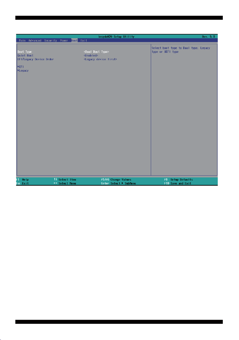
4-9 Boot
Boot type
Select boot type for Dual type ,Legacy boot type or UEFI boot type, default is Dual boot type
Quiet Boot
The optional settings are: Enabled(default), Disabled.
EFI / Legacy Device order
Determine EFI device fi rst or legacy device fi rst.
The optional settings: EFI device fi rst, Legacy device fi rst(default), smart mode
59
Page 65

4-9-1 Legacy
Normal Boot Menu
Select Normal Boot option priority or Advance Boot option priority.
The optional settings: Normal(default), Advance
60
Page 66

Boot Type Order
Setting the boot type priority.
The default settings is 1.USB drive 2.Hard Disk Drive 3.CD/DVD ROM drive 4.Others
61
Page 67

4-10 EXIT
Exit Saving Changes
This item allows user to reset the system after saving the changes.
Save Change Without Exit
This item allows user to saving the changes but doesn’t restart.
Exit Discard Changes
This item allows user restart the system but no saving the changes
Load Optimal Default
Use this item to restore the optimal default for all the setup options.
Discare Changes
Use this item to cancel all the setup options.
62
Page 68

4-11 Device Manager
Please press the key F10 when bootup to go into the Device Manager menu
Serial Port 1/2 Confi guration
Please refer section 4-11-1
63
Page 69

4-11-1 SIO FINTEK81801U
Serial Port 1/2
Use this item to enable or disable serial port (COM1,COM2)
The optional settings are: Enabled(default), Disabled.
Serial Port 1 Base IO Address / Interrupt / Serial Mode
Use this item to select an optimal setting for super IO device.
The optional settings are:
IO=3F8h; IRQ=4 (default)
IO=3F8h; IRQ=3,4
IO=2E8h; IRQ=3,4
IO=2F8h; IRQ=3,4
IO=3E8h; IRQ=3,4
Serial Port 2 Base IO Address / Interrupt / Serial Mode
Use this item to select an optimal setting for super IO device.
The optional settings are:
IO=2F8h; IRQ=3 (default)
IO=3F8h; IRQ=3,4
IO=2E8h; IRQ=3,4
IO=2F8h; IRQ=3,4
IO=3E8h; IRQ=3,4
64
Page 70

Serial Mode
RS232 driver(default) :
When hardware select to RS232 or RS422 mode, please enter to RS232 driver.
RS485 driver: When hardware select to RS485 mode,
please enter to RS485 driver. It is the auto fl ow function for RS485.
Power Failure
This item specifi es whether your system will reboot after a power failure or interrupt occurs.
[Keep state] Restores the system to the status before power failure or interrupt occurred. (default)
[Always on] Leaves the computer in the power on state.
[Always off] Leaves the computer in the power off state.
Hardware Monitor
Press [Enter] to view PC health status.
This section shows the status of your CPU, Fan, and overall system.
This is only available when there is Hardware Monitor function onboard.
65
Page 71

Chapter-5
DRIVER INSTALLATION
There is a system installation DVD in the package. This DVD does not only include all the
drivers you need but also some other free application programs and utility programs.
In addition, this DVD also includes an auto detect software telling you which hardware is
installed and which driver is needed so that your system can function properly. We call this
auto detect software SYSTEM INSTALL.
SYSTEM INSTALL Supports Windows 7(32bit/64bit) / Windows
8/8.1(32bit/64bit)
Insert the DVD into your DVD-ROM drive and the SYSTEM INSTALL menu should appear
as below. If the menu does not appear, double-click MY COMPUTER and double-click
DVD-ROM drive or click START, click RUN, and type X:\SETUP.EXE
(assuming your DVD-ROM drive is X).
Make your selection from SYSTEM INSTALL menu:
1. Auto Detect Main board and OS to AUTOMATIC DRIVER INSTALLATION menu
2. Browse DVD to view the contents of the DVD
3. Exit to exit SYSTEM INSTALL menu
66
Page 72

AUTOMATIC DRIVER INSTALLATION menu
1. INF Install Intel Baytrail chipset driver
2. VGA Install onboard VGA driver
3. Serial IO Install Serial IO driver (FOR Win 7 only)
4. xHCI Install Intel USB 3.0 xHCI driver (FOR Win 7 only)
5. HD Audio Install HD Audio Codec driver
6. MBI Install MBI driver (FOR Win 8/8.1 only)
7. LAN To the LAN driver Readme fi le
8. TXE Patch Install Intel TXE patch (FOR Win 7 only)
9. TXE Install Intel TXE driver
Each selection is illustrated below:
67
Page 73

5-1 INF Install Intel Baytrail Chipset Driver
(example for WIN8 64bit)
1. At the "AUTOMATIC DRIVER INSTALLATION
menu" screen, click "INF".
3. At the "License Agreement" screen,
click "Yes"
2. At the "Intel® Chipset Device Software"
screen, click "Next".
4. At the "Readme File Information" screen,
Click "Next".
68
Page 74

5. Click "Next"
NOTE: SYSTEM INSTALL will auto detect fi le path
For Windows 7 64/32-bit,
X:\driver\INTEL\BAY\INF\WIN7\infi nst_autol.exe
For Windows 8 / 8.1 32/64-bit
X:\driver\INTEL\BAY\INF\WIN_8_64\infi nst_autol.exe
6. Click "Finish" & restart computer.
69
Page 75

5-2 VGA Install Intel Baytrail VGA Driver
(example for WIN8 64bit)
1. At the"AUTOMATIC DRIVER INSTALLATION
menu"screen, click "VGA".
3. At the "License Agreement" screen,
Click "Yes"
2. At the "Welcome to the Setup Program
screen, Click "Next".
4. At the "Readme File Information"
screen, Click "Next"
70
Page 76

5. At the "Setup Progress" screen,
Click "Next".
NOTE: SYSTEM INSTALL will auto detect fi le path
For Windows 7 32-bit,
X:\driver\INTEL\BAY\VGA\WIN_7_32\Setup.exe
For Windows 7 64-bit
X:\driver\INTEL\BAY\VGA\WIN_7_64\Setup.exe
For Windows 8 / Windows 8.1 32-bit
X:\ \driver\INTEL\BAY\VGA\WIN_8_32\Setup.exe
For Windows 8 / Windows 8.1 64-bit
X:\driver\INTEL\BAY\VGA\WIN_8_64\Setup.exe
6. Click "Finish" to restart computer
71
Page 77

5-3 Serial IO Install Driver Baytrail Serial IO Driver
(FOR Windows 7 only)
1. At the "AUTOMATIC DRIVER INSTALLATION
menu" screen, click "Serial IO".
3. At the "License Agreement" screen,
Click "Yes"
2. At the "Welcome to the Setup Program
screen, Click "Next".
4. At the "Setup type" screen, select "complete"
and Click "Next".
72
Page 78

5. At the "Ready to install the program" screen,
Click "Install"
NOTE: SYSTEM INSTALL will auto detect fi le path
For Windows 7 32-bit,
X:\driver\INTEL\BAY\SERIALIO\WIN7_32Bit.msi
For Windows 7 64-bit
X:\driver\INTEL\BAY\SERIALIO\Win7_64Bit.msi
6. Click "Finish" and restart computer
73
Page 79

5-4 xHCI Install Intel USB 3.0 xHCI Driver (FOR Windows 7 only)
1. At the "AUTOMATIC DRIVER INSTALLATION
menu" screen, click "xHCI".
3. At the "License Agreement" screen,
Click "Yes".
2. At the "Welcome to the Setup Program
screen, Click "Next".
4. At the "Readme File Information" screen,
Click "Next".
74
Page 80

5. At the "Setup Progress" screen, Click "Next".
NOTE: SYSTEM INSTALL will auto detect fi le path
For Windows 7 32 / 64-bit,
X:\driver\INTEL\BAY\XHCI\Driver_Installer\Setup.exe
6. Click "Finish" to restart computer
75
Page 81

5-5 HD Audio Install High Defi nition Audio Driver
(example for WIN8 64bit)
1. At the "AUTOMATIC DRIVER INSTALLATION
menu", click "HD Audio"
3. Click "Finish" to restart computer
NOTE: SYSTEM INSTALL will auto detect fi le path
For Windows 7 32 / 64-bit, Windows 8/8.1 32 / 64-bit
X:\driver\INTEL\BAY\SOUND\Win7_Win8_Win81_R273.exe
2. Click" Next".
76
Page 82

5-6 MBI Install Intel MBI Driver (FOR Win 8/8.1 only)
1. At the "AUTOMATIC DRIVER INSTALLATION
menu", click "HD Audio".
3. At the "License Agreement" screen,
Click "Yes".
2. At the "Welcome to the Setup Program
screen, Click "Next".
4. At the "Setup Progress" screen, Click "Next".
77
Page 83

5. Click "Finish" to restart computer
NOTE: SYSTEM INSTALL will auto detect fi le path
For Windows 8/8.1 32 / 64-bit,
X:\driver\INTEL\BAY\MBI\Setup.exe
78
Page 84

5-7 TXE Install Intel TXE driver
5-7-1 TXE Install for WIN8/WIN8.1
1. At the "AUTOMATIC DRIVER INSTALLATION
menu", click "TXE".
3. At the "License Agreement" screen,
Click "Yes".
2. At the "Setup" screen, Click "Next".
4. Click "Next".
79
Page 85

5. Click "Finish" & restart computer
NOTE: SYSTEM INSTALL will auto detect fi le path
For Windows 8 32 / 64-bit,
X:\driver\INTEL\BAY\TXE\WIN_8\SetupTXE.exe
For Windows 8.1 32 / 64-bit,
X:\driver\INTEL\BAY\TXE\WIN_8.1\SetupTXE.exe
80
Page 86

5-7-2 TXE Install for WIN7
Please install PXE Patch fi rst.
1. At the "AUTOMATIC DRIVER INSTALLATION
menu", click "TXE Patch".
3. Click “Finish” & restart computer
2. At the "Windows Update" screen,
Click "Yes".
4. At the "AUTOMATIC DRIVER INSTALLATION
menu", click "TXE "
81
Page 87

5. At the "TXE Setup" screen, Click "Next".
6. At the "License Agreement" screen,
Click "Yes".
7. Click "Next".
NOTE: SYSTEM INSTALL will auto detect fi le path
For Windows 7 32 / 64-bit,
TXE Patch
X:\driver\INTEL\BAY\TXE\WIN_7\kmdf-1.11-Win-6.1-x86.msu
X:\driver\INTEL\BAY\TXE\WIN_7\kmdf-1.11-Win-6.1-x64.msu
TXE
X:\driver\INTEL\BAY\TXE\WIN_7\SetupTXE.exe
X:\driver\INTEL\BAY\TXE\WIN_7\SetupTXE.exe
8. Click "Finish" & restart computer
82
Page 88

5-8 How to update Insyde BIOS
Under DOS Mode
STEP 1. Prepare a bootable disc.
(Storage device could be USB FDD or USB pen drive.)
STEP 2. Copy utility program to your bootable disc. You may download it from our website.
STEP 3. Copy the latest BIOS for your LEX motherboard from our website to
your bootable disc.
STEP 4. (Here take 3I380D as an example, please enter your motherboard’s name)
Insert your bootable disc into X: (X could be C:, A: or others.
It depends on which type of storage device you use. )
Start the computer and type
X:\〉H2OFFT-D.EXE 3I380DA2.ROM –BIOS -ALL
3I380DA2.ROM is the fi le name of the latest BIOS.
It may be 3I380DA1.ROM or 3I380DA2.ROM, etc.
Please leave one space between .ROM & -BIOS -ALL
By Bay Trail series mainboard, please type
X:\〉H2OFFT-D.EXE 3I380DA2.ROM –BIOS -ALL
-BIOS : Flash BIOS region
-ALL : Flash all
STEP 5. Press ENTER and the BIOS will be updated,
Computer will restart automatically.
83
Page 89

Appendix A: Power Consumption Test
Condition
Item Spec
CPU Atom E3815 1.46 Ghz
Memory DDR3L 1066 2GB
Operating System Windows 7 / SP1
Test Program 3D Mark 06
HDD 2.5" SATA Slim Type HDD
mSATA 32GB
Test Result for reference only !
Slim Type HDD
Power off
0.03A 0.79A 0.5A 0.86A 0.66A
Start up
Maximum
Stable
Operation
Maximum
E3815
mS ATA
0.03A 0.64A 0.45A 0.73A 0.56A
The power consumption depends on your device choice!
Shut down
Maximum
84
Page 90

Condition
Item Spec
CPU Celeron J1900 2 Ghz
Memory DDR3L 1333 4GB
Operating System Windows 7 / SP1
Test Program 3D Mark Vantage
HDD 2.5" SATA Slim Type HDD
mSATA 32GB
Test Result for reference only !
Power off
Start up
Maximum
Stable
Operation
Maximum
Shut down
Maximum
Slim Type HDD
0.03A 0.84A 0.52A 1.31A 0.8A
J1900
mS ATA
0.03A 0.79A 0.5A 1.15A 0.68A
The power consumption depends on your device choice!
85
Page 91

Appendix B: Resolution list
640 x 480 x ( 256 / 16bit / 32bit )
800 x 600 x ( 256 / 16bit / 32bit )
1024 x 768 x ( 256 / 16bit / 32bit )
1152 x 864 x ( 256 / 16bit / 32bit )
1280 x 600 x ( 256 / 16bit / 32bit )
1280 x 720 x ( 256 / 16bit / 32bit )
1280 x 768 x ( 256 / 16bit / 32bit )
1280 x 800 x ( 256 / 16bit / 32bit )
1280 x 960 x ( 256 / 16bit / 32bit )
1280 x 1024 x ( 256 / 16bit / 32bit )
1400 x 1050 x ( 256 / 16bit / 32bit )
1440 x 900 x ( 256 / 16bit / 32bit )
1600 x 900 x ( 256 / 16bit / 32bit )
1600 x 1200 x ( 256 / 16bit / 32bit )
1680 x 1050 x ( 256 / 16bit / 32bit )
1920 x 1080 x ( 256 / 16bit / 32bit )
1920 x 1200 x ( 256 / 16bit / 32bit )
86
Page 92

Appendix C: F75111N I C DIO device
2
1-1 IO Device: F75111 under Windows
The Sample code source you can download from
Source fi le: F75111_DIOSrc.rar
Binary fi le: F75111_DemoBin.rar
USERNAME & PASSWORD: sf
How to use this Demo Application
http://tprd.info/lexwiki/index.php/IO_Device:F75111
1. Press the "Start" button to test DIO function
2. Press the "Enable" button to test WDT function
3. Press the "Disable" button to disable WDT
4. Check the "Enable Loop" box and press "Enable" to do WDT loop test
5. Press "Install WDT" to set the system to autorun this application when booting,
press again to remove this application when booting.
6. If WDT enable, system icon will be . if disable, system icon will be
87
Page 93

p.s.
f75111 send "F75111_SetWDTEnable(BYTE byteTimer)" including a parameter "timer",
if there's no disable signal (F75111_SetWDTDisable()) to stop it before timer countdown to 0, System will reboot.
if there's disable signal received, resent Enable WDT signal, for a loop to prevent from reboot
Introduction
Initial Internal F75111 port address (0x9c)
defi ne GPIO1X, GPIO2X, GPIO3X to input or output
and Enable WDT function pin
Set F75111 DI/DO ( sample code as below Get Input value/Set output value )
DO: InterDigitalOutput(BYTE byteValue))
DI: InterDigitalInput()
Enable/Disable WDT
Enable : F75111_SetWDTEnable (BYTE byteTimer)
Disable: F75111_SetWDTDisable ()
PULSE mode
Sample to setting GP33, 32, 31, 30 output 1mS low pulse signal.
{
this->Write_Byte(F75111_INTERNAL_ADDR, GPIO3X_PULSE_CONTROL, 0x00); //This is setting low pulse output
this->Write_Byte(F75111_INTERNAL_ADDR, GPIO3X_PULSE_WIDTH_CONTROL, 0x01); //This selects the pulse width to 1mS
this->Write_Byte(F75111_INTERNAL_ADDR, GPIO3X_CONTROL_MODE, 0x0F); //This is setting the GP33, 32, 31, 30 to output function.
this->Write_Byte(F75111_INTERNAL_ADDR, GPIO3X_Output_Data , 0x0F); //This is setting the GP33, 32, 31, 30 output data.
}
Sample to setting GP33, 32, 31, 30 output 1mS low pulse signal.
void F75111::InitInternalF75111()
{
this->Write_Byte(F75111_INTERNAL_ADDR,GPIO1X_CONTROL_MODE ,0x00); //set GPIO1X to Input function
this->Write_Byte(F75111_INTERNAL_ADDR,GPIO3X_CONTROL_MODE ,0x00); //set GPIO3X to Input function
this->Write_Byte(F75111_INTERNAL_ADDR,GPIO2X_CONTROL_MODE ,0xFF); //set GPIO2X to Output function
this->Write_Byte(F75111_INTERNAL_ADDR,F75111_CONFIGURATION, 0x03); //Enable WDT OUT function
}
88
Page 94

Set output value
void F75111::InterDigitalOutput(BYTE byteValue)
{
BYTE byteData = 0;
byteData = (byteData & 0x01 )? byteValue + 0x01 : byteValue;
byteData = (byteData & 0x02 )? byteValue + 0x02 : byteValue;
byteData = (byteData & 0x04 )? byteValue + 0x04 : byteValue;
byteData = (byteData & 0x80 )? byteValue + 0x08 : byteValue;
byteData = (byteData & 0x40 )? byteValue + 0x10 : byteValue;
byteData = (byteData & 0x20 )? byteValue + 0x20 : byteValue;
byteData = (byteData & 0x10 )? byteValue + 0x40 : byteValue;
byteData = (byteData & 0x08 )? byteValue + 0x80 : byteValue; // get value bit by bit
this->Write_Byte(F75111_INTERNAL_ADDR,GPIO2X_OUTPUT_DATA,byteData); // write byteData value via GPIO2X output pin
}
Get Input value
BYTE F75111::InterDigitalInput()
{
BYTE byteGPIO1X = 0;
BYTE byteGPIO3X = 0;
BYTE byteData = 0;
this->Read_Byte(F75111_INTERNAL_ADDR,GPIO1X_INPUT_DATA,&byteGPIO1X) ; // Get value from GPIO1X
this->Read_Byte(F75111_INTERNAL_ADDR,GPIO3X_INPUT_DATA,&byteGPIO3X) ; // Get value from GPIO3X
byteGPIO1X = byteGPIO1X & 0xF0; // Mask unuseful value
byteGPIO3X = byteGPIO3X & 0x0F; // Mask unuseful value
byteData = ( byteGPIO1X & 0x10 )? byteData + 0x01 : byteData;
byteData = ( byteGPIO1X & 0x80 )? byteData + 0x02 : byteData;
byteData = ( byteGPIO1X & 0x40 )? byteData + 0x04 : byteData;
byteData = ( byteGPIO3X & 0x01 )? byteData + 0x08 : byteData;
byteData = ( byteGPIO3X & 0x02 )? byteData + 0x10 : byteData;
byteData = ( byteGPIO3X & 0x04 )? byteData + 0x20 : byteData;
byteData = ( byteGPIO3X & 0x08 )? byteData + 0x40 : byteData;
byteData = ( byteGPIO1X & 0x20 )? byteData + 0x80 : byteData; // Get correct DI value from GPIO1X & GPIO3X
return byteData;
}
Enable WatchDog
void F75111_SetWDTEnable (BYTE byteTimer)
{
WriteByte(F75111_INTERNAL_ADDR,WDT_TIMER_RANGE ,byteTimer); // set WatchDog range and timer
WriteByte(F75111_INTERNAL_ADDR,WDT_CONFIGURATION,WDT_TIMEOUT_FLAG | WDT_ENABLE | WDT_PULSE | WDT_PSWIDTH_100MS);
// Enable WatchDog, Setting WatchDog confi gure
}
89
Page 95

Disable WatchDog
void F75111_SetWDTDisable ()
{
WriteByte(F75111_INTERNAL_ADDR,WDT_CONFIGURATION,0x00); // Disable WatchDog
}
1-2 IO Device: F75111 VB6 under Windows
The Sample code source you can download from
Source fi le: 75111_VB_v10.rar
Binary fi le: 75111_VB_Src.rar
USERNAME & PASSWORD: sf
How to use this Demo Application
http://tprd.info/lexwiki/index.php/IO_Device:F75111_VB6
A Function - Enable WDT timer ,Key-in the value by seconds then system will reboot after
value which you key-in in left text box !!
B Function - Disable WDT timer ,Push down the button then WDT timer value will be clear !!
C Function - Set DO Value ,Key-in the DO value by hex then push the button !!
D Function - Check DI Value ,The right side two text box will display DI 1X & 2X Value
when you push down the button!!
90
Page 96

SDK Function Introduction
Function EnableWDT
Function EnableWDT(timer As Integer)
Call WriteI2CByte(&H3, &H3)
Call WriteI2CByte(&H37, timer)
Call WriteI2CByte(&H36, &H73)
End Function
Function DisableWDT
Function DisableWDT()
Call WriteI2CByte(&H36, &H0)
End Function
Function SetDOValue
Function SetDOValue(dovalue As Integer)
Call WriteI2CByte(&H23, &H0)
Call WriteI2CByte(&H20, &HFF)
Call WriteI2CByte(&H2B, &HFF)
Call WriteI2CByte(&H21, dovalue)
End Function
Function CheckDIValue
Function CheckDIValue()
Dim GPIO1X As Integer
Dim GPIO3X As Integer
Dim DI1Xhex As String
Dim DI3Xhex As String
Call ReadI2CByte(&H12, GPIO1X)
Call ReadI2CByte(&H42, GPIO3X)
DI1Xhex = Hex(GPIO1X)
DI3Xhex = Hex(GPIO3X)
Text3.Text = "0x" + DI1Xhex
Text4.Text = "0x" + DI3Xhex
End Function
91
Page 97

1-3 IO Device: F75111 under linux
The Sample code source you can download from
Source fi le: F75111v2.0L.tar.gz
Binary fi le: F75111v2.0LBin.tar.gz
USERNAME & PASSWORD: sf
How to compile source code
1. Compile source code with Code::Blocks
download and install the Code::Block with command "apt-get install codeblocks"
Open an exist project(F75111.cbp) in Code::Blocks, click the compile button
( add an option 'pkg-confi g --libs gtk+-2.0 gthread-2.0' in "Project->Build Option->
Linker Setting->Other linker option")
2. Compile source code with "make"
1.cd F75111
1.make
1.src/f75111 // execute the binary fi le
How to use this Demo Application
http://tprd.info/lexwiki/index.php/IO_Device:F75111_under_linux
92
Page 98

1. Press the "Start" button to test DIO function
2. Press the "Enable" button to test WDT function
3. Press the "Disable" button to disable WDT
4. Check the "Enable Loop" box and press "Enable" to do WDT loop test
5. Press "Install" to set the system to autorun this application when booting,
press "Uninstall" to remove this application when booting.
6. If WDT enable, system icon will be blinking.
p.s.
f75111 send "F75111_SetWDTEnable(BYTE byteTimer)" including a parameter "timer",
if there's no disable signal (F75111_SetWDTDisable()) to stop it before timer countdown to 0, System will reboot.
if there's disable signal received, resent Enable WDT signal, for a loop to prevent from reboot p.s.
Introduction
IO function In fi le SMBus.c
void SMBusIoWrite(BYTE byteOffset,BYTE byteData)
{
outb( byteData , m_SMBusMapIoAddr + byteOffset);
}
BYTE SMBusIoRead(BYTE byteOffset)
{
DWORD dwAddrVal;
dwAddrVal = inb(m_SMBusMapIoAddr + byteOffset);
return (BYTE)(dwAddrVal & 0x0FF);
}
Initial internal F75111
void F75111::InitInternalF75111()
{
this->Write_Byte(F75111_INTERNAL_ADDR,GPIO1X_CONTROL_MODE ,0x00); //set GPIO1X to Input function
this->Write_Byte(F75111_INTERNAL_ADDR,GPIO3X_CONTROL_MODE ,0x00); //set GPIO3X to Input function
this->Write_Byte(F75111_INTERNAL_ADDR,GPIO2X_CONTROL_MODE ,0xFF); //set GPIO2X to Output function
this->Write_Byte(F75111_INTERNAL_ADDR,F75111_CONFIGURATION, 0x03); //Enable WDT OUT function
}
93
Page 99

Set output value
void F75111::InterDigitalOutput(BYTE byteValue)
{
BYTE byteData = 0;
byteData = (byteData & 0x01 )? byteValue + 0x01 : byteValue;
byteData = (byteData & 0x02 )? byteValue + 0x02 : byteValue;
byteData = (byteData & 0x04 )? byteValue + 0x04 : byteValue;
byteData = (byteData & 0x80 )? byteValue + 0x08 : byteValue;
byteData = (byteData & 0x40 )? byteValue + 0x10 : byteValue;
byteData = (byteData & 0x20 )? byteValue + 0x20 : byteValue;
byteData = (byteData & 0x10 )? byteValue + 0x40 : byteValue;
byteData = (byteData & 0x08 )? byteValue + 0x80 : byteValue; // get value bit by bit
this->Write_Byte(F75111_INTERNAL_ADDR,GPIO2X_OUTPUT_DATA,byteData); // write byteData value via GPIO2X output pin
}
Get Input value
BYTE F75111::InterDigitalInput()
{
BYTE byteGPIO1X = 0;
BYTE byteGPIO3X = 0;
BYTE byteData = 0;
this->Read_Byte(F75111_INTERNAL_ADDR,GPIO1X_INPUT_DATA,&byteGPIO1X) ; // Get value from GPIO1X
this->Read_Byte(F75111_INTERNAL_ADDR,GPIO3X_INPUT_DATA,&byteGPIO3X) ; // Get value from GPIO3X
byteGPIO1X = byteGPIO1X & 0xF0; // Mask unuseful value
byteGPIO3X = byteGPIO3X & 0x0F; // Mask unuseful value
byteData = ( byteGPIO1X & 0x10 )? byteData + 0x01 : byteData;
byteData = ( byteGPIO1X & 0x80 )? byteData + 0x02 : byteData;
byteData = ( byteGPIO1X & 0x40 )? byteData + 0x04 : byteData;
byteData = ( byteGPIO3X & 0x01 )? byteData + 0x08 : byteData;
byteData = ( byteGPIO3X & 0x02 )? byteData + 0x10 : byteData;
byteData = ( byteGPIO3X & 0x04 )? byteData + 0x20 : byteData;
byteData = ( byteGPIO3X & 0x08 )? byteData + 0x40 : byteData;
byteData = ( byteGPIO1X & 0x20 )? byteData + 0x80 : byteData; // Get correct DI value from GPIO1X & GPIO3X
return byteData;
}
94
Page 100

Enable WatchDog
void F75111_SetWDTEnable (BYTE byteTimer)
{
WriteByte(F75111_INTERNAL_ADDR,WDT_TIMER_RANGE ,byteTimer); // set WatchDog range and timer
WriteByte(F75111_INTERNAL_ADDR,WDT_CONFIGURATION,WDT_TIMEOUT_FLAG | WDT_ENABLE | WDT_PULSE | WDT_PSWIDTH_100MS);
// Enable WatchDog, Setting WatchDog confi gure
}
Disable WatchDog
void F75111_SetWDTDisable ()
{
WriteByte(F75111_INTERNAL_ADDR,WDT_CONFIGURATION,0x00); // Disable WatchDog
}
95
 Loading...