

LENOVO A2010-a Service manual

Lenovo A2010-a
Service Manual

Contents
1 Layout of main board ................................................................................................................. 3
1.1 Layout ................................................................................................................................. 3
1.2 Mobile phone principle and fault analysis ........................................................................... 4
1.3 Baseband unit ..................................................................................................................... 5
1.3.1 Does not boot ........................................................................................................... 5
1.3.2 LCD .......................................................................................................................... 8
1.3.3 CTP ........................................................................................................................ 10
1.3.4 Flash ....................................................................................................................... 11
1.3.5 MAIN CAMERA ...................................................................................................... 12
1.3.6 SUB CAMERA ........................................................................................................ 13
1.3.7 KEY ........................................................................................................................ 15
1.3.8 VIB .......................................................................................................................... 15
1.3.9 RECEIVER ............................................................................................................. 16
1.3.10 SPEAKER ............................................................................................................. 17
1.3.11 MIC ....................................................................................................................... 18
1.3.12 Earphone failure ................................................................................................... 20
1.3.13 SIM_CARD ........................................................................................................... 20
1.3.14 G-SENSOR ........................................................................................................... 22
1.3.15 BT/WIFI/FM/GPS .................................................................................................. 22
1.3.16 RF unit .................................................................................................................. 26
1.3.17 GSM failure ................................ ................................ ................................ ........... 26
1.3.18 WCDMA failure ..................................................................................................... 27
1.3.19 LTE failure ............................................................................................................. 29
2 Assembly and disassembly instructions ...................................................................................... 32
2.1 Disassembly ..................................................................................................................... 32
2.1.1 Disassemble battery cover...................................................................................... 32
2.1.2 Remove the battery ................................................................................................ 32
2.1.3 Disassemble rear cover .......................................................................................... 32
2.1.4 Loosen the MIC ...................................................................................................... 33
2.1.5 Loosen the speaker ................................................................................................ 34
2.1.6 Loosen the vibrator ................................................................................................. 34
2.1.7 Dismantle the LCD connector ................................................................................. 35
2.1.8 Dismantle side key FPC connector ......................................................................... 35
2.1.9 Dismantle TP connector .......................................................................................... 36
2.1.10 Dismantle rear camera connector ......................................................................... 36
2.1.11 Loosen the MB screws .......................................................................................... 36
2.1.12 Separate MB front TP&LCD assembly .................................................................. 37
2.1.13 De-soldering speaker ............................................................................................ 37
2.1.14 Dismantle front camera ......................................................................................... 38
2.1.15 De-soldering receiver and remove ........................................................................ 38
2.1.16 De-soldering vibrator ............................................................................................ 38
2.1.17 De-soldering MIC .................................................................................................. 39
2.1.18 Tilt TP FPC ........................................................................................................... 39
2.1.19 Dismantle side key ................................................................................................ 39
2.1.20 Dismantle camera lens ......................................................................................... 40
2.1.21 Tear down battery compartment Mylar .................................................................. 40
2.1.22 Summary of demolition materials .......................................................................... 41
2.2 Assembly guide ................................................................ ................................ ................. 41
1.1 Layout
1 Layout of main board

1.2 Mobile phone principle and fault analysis
MT6735 baseband chip as illustrated
:
MediaTek MT6735 SoC integrates four 64 ARMv8 architecture Cortex-A53 CPU core, clocked at
1.5GHz, while integrating the next generation of GPU Mali-T720,8 core, support for OpenGL ES 3.0,
OpenCL 1.2.
The biggest highlight of the baseband processor part to support GSM / EVDO Rev. A / CDMA2000 1x /
TD-SCDNA / WCDMA / TD-LTE / LTE FDD standard, including EVDO Rev. A / CDMA2000 1x is the first
time in the SOC MediaTek , patents from vIA Telecom.
Multimedia, supports low-power 1080p / 30fps video playback and recording, H.265 / H.264 video
encoding, integrated 13 million pixel camera ISP, supports PIP PIP, VIV dual video, Video Face Beautifier,
also supports ClearMotion, MiraVision.
Wireless technology supports dual-band Wi-Fi, Bluetooth 4.0.

1.3 Baseband unit
1.3.1 Does not boot
boot sequence
The Principle:
Phone is switched on in the process as shown above, press the power button, PWRKEY detected
low latency 30ms, drive power management chip LDO open and the brightest to the baseband circuitry,
starting from Vcore, 2ms interval turn on power to VMCH power-end. At the same time, from the
beginning of the end electrical power management chip RESET signal resets 200ms after the Vcore,
the baseband chip to boot into software startup program, complete boot.
In addition, this platform Power Good detection function. That PMIC will automatically detect each
way power output, the power output if there is not, PMIC will repeat the process on power. If this
phenomenon occurs, the performance of reset signal remains low.
boot process
1. Mobile phone power supply: mobile phone plus battery or DC power supply, power management chip
(PMU) to get the battery voltage, its internal 32KHz watch crystal module to work, the output voltage of the
external RTC's work, for real-time clock crystal start-up.
2. Phone reset: press the power button, after PMU detected RST_ON outputs a reset signal to the
phone CPU, CPU will start the system self-test program;
3. The working voltage output: After the phone to complete the self-test, CPU PMU output by IIC bus
control circuit voltage of each cell phone, such as VDD1, VDD2, VDD3, AVDD and the like;
4. 13M crystal work: After the clock and get a job working voltage, CPU outputs REF_ON signals to
control the work of 13M circuit generates 13MHz clock, on the one hand to provide work master CPU clock,
on the other hand to provide the main chip radio frequency reference frequency source ;
5. Call the boot process: After the CPU self-test completed and the operating voltage and the master
clock, via IIC bus calibration work PMU output voltage from various quarters, the calibration is complete, it
will output chip select signals and address signals to FLASH, calling boot process , and boot;
6. Establishing a communication connection: the phone is turned on, CPU call RF parameters from
FLASH, the received signal strength of a cell through the broadcast control channel (BCCH), if there is a
SIM card or UIM card in the phone, the relevant information is transmitted to the adjacent base station, and
receives information from the base station, which is connected with the corresponding networks, known as
search network;
7.After completion of the standby search network, the phone will be in a wait state, the phone will
periodically during the exchange of information with the base station via a number of auxiliary slow control
channel (SACCH), such as signal strength, frequency synchronization, reception quality and reception level
Failure analysis processing
1. For the failure does not boot, the first detection of the battery interfaces for any obvious damage. If
the battery interface OK, then use the DC power supply to the mobile phone, observe current fault plane;
:

2. With a test fixture measurement bad motherboard power current
Current
inspection
Check
U401
Check
X401
<70mA
Welding
U401
Replace
U401
100~300mA
Replace
U401
Re-downlo
ad software
70~100mA
Replace
U401
Replace
U101
Replace
U602
OK
OK
OK
Y
N
N N N
Y Y N Y Y
:
The current is too large (typically greater than 1A), proved short-circuit motherboard, usually battery
Vbat pin connector is shorted to ground, can be removed U401 (PMIC) and then measuring the Vbat pin is
short-circuited, then turn on the replacement Vbat path other chip U901 (flash drive), U805 (backlight driver)
and then measuring the Vbat pin is shorted;
A current at 70mA or less, to check each power supply is normal, usually PMIC, clock circuit Weld or
damaged, you can measure the crystal is normal;
A current of 70 ~ 100mA, typically software data loss, half rubbing upgrade software;
d, current is 100 ~ 300mA, check the clock (X401) is normal, focus on examination PMIC (U401), CPU
(U101), MEMORY (U602) welding is bad
Flow chart:
Circuit Schematic:

Not charge
Replace USB
connector
Replace R509
Replace PMIC
Check VCHG
Voltage
N
Y
N
N
Y
Check
current
Check the
charging IC
Replace U501
Y
Charge management chip U501, when checking the charging voltage, a signal is sent to the PMIC and
start charging, charging current is monitored by ISENSE, VBAT monitor the battery voltage:
After inserting the battery charger, the phone no response, can not be charged, first replace the battery
and charging cable for testing; and then measuring the charge current is normal; and then try to add or
replace welding U502, and then try to add another weld or replace PMIC.
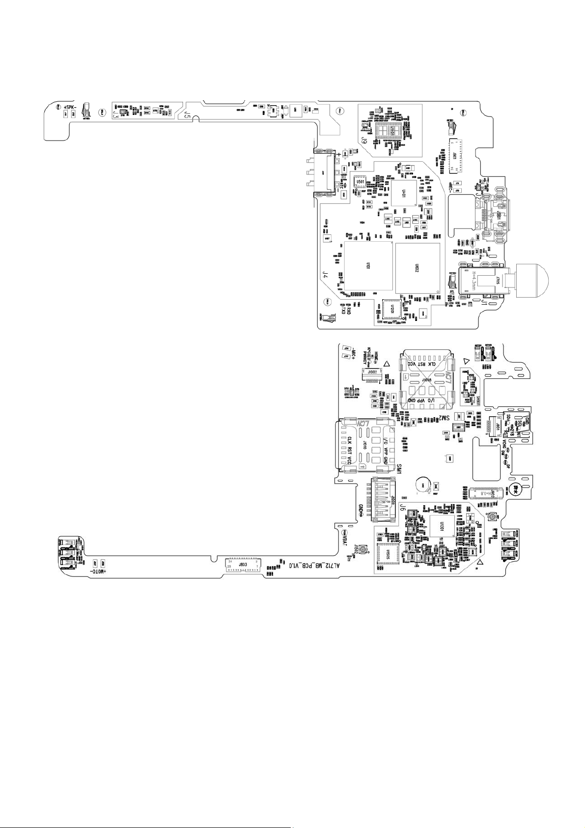
1.3.2 LCD
LCD Display
bad
Reassemble
LCD
Check J802 Is
abnormal
Upgrade or
replace
Replace LCD
Replacing
Devices
OK
Y
N Y N
Circuit schematics:
LCD is MIPI interface, including power/data/clock/reset. The main screen LCD display circuit MIPI
interfaces are generally used communication interfaces. Each signal is described as follows:
TDP/TDN is MIPI data interface/TCP/TCN for the MIPI clock interface; VIO18_PMU control signal
voltage power supply; LCM_RST reset; LED_A, LED_K backlight power supply.
Fault analysis process:
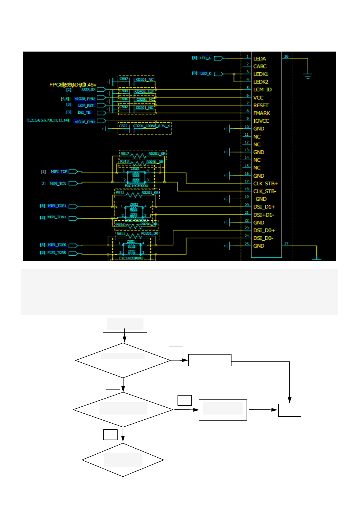
Black screen, black and white, the video screen display dislocation
Blacklight Driver
Analysis process:
Gray screen fault plane generally weak backlight, which is due to the backlight driving voltage is not
enough cause, measuring LED-A in the phone is switched mode voltage is 36V. Measurement is not
L802/D807/U805 device abnormal.
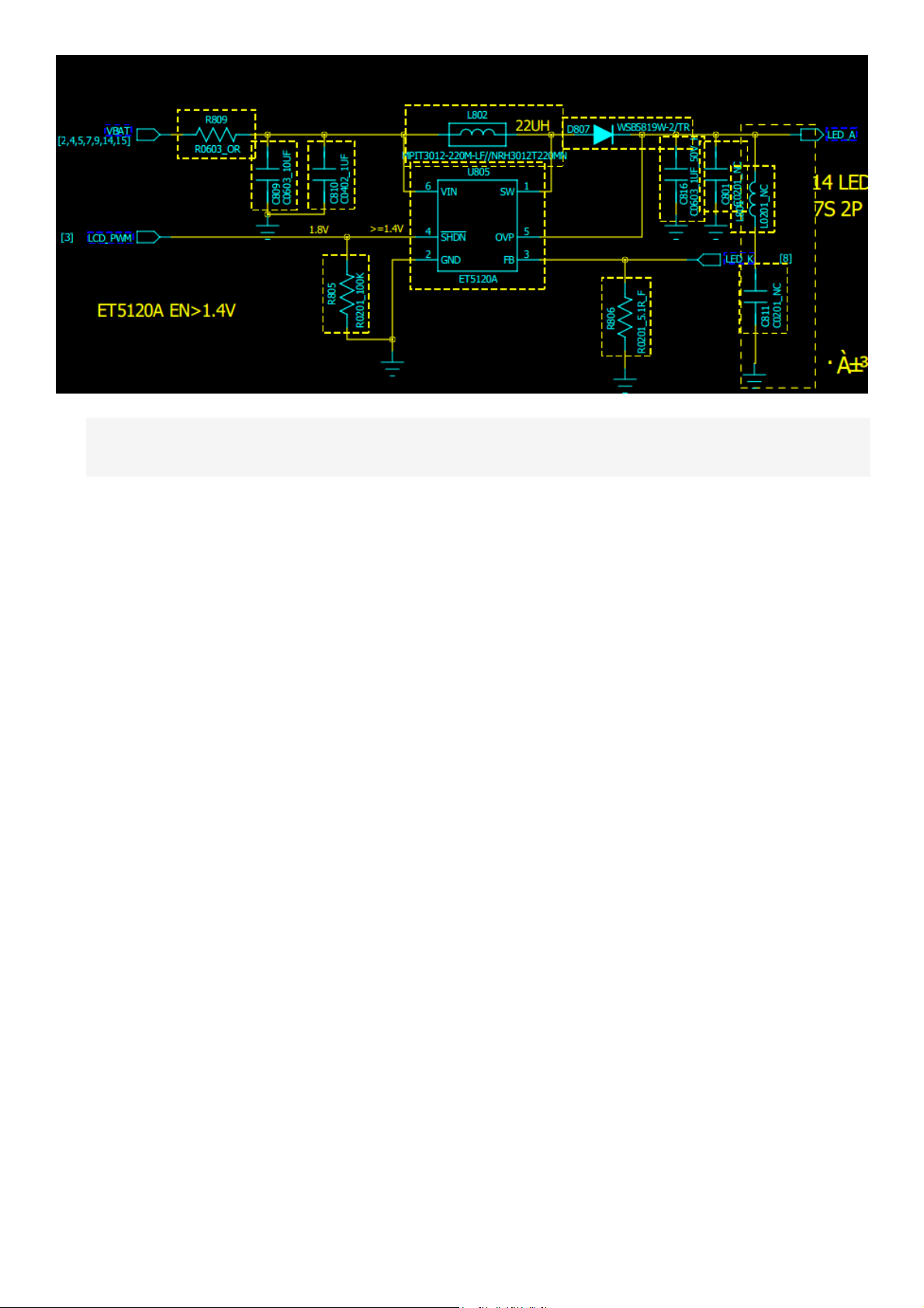
1.3.3 CTP
Circuit Schematics
Capacitive touch screen technology CTP (Capacity Touch Panel) is used by the body to work in the
current sense. Capacitive screen is a four-layer composite glass screen, the inner surface of the glass panel
and the sandwich and coated with a layer ITO (indium tin oxide nano), the outermost layer is a protective
layer of silica glass only 0.0015mm thick, laminated ITO coating for the face, leads the four corners four
electrodes, the inner layer of ITO as a screen to ensure that the work environment. Power supply circuit
VIO18_PMU/VIO_28PMU, control signal GPIO_CTP_RSTB/EINT_CTP/I2C bus SDA1 and SCL1.
Failure analysis:
1. Replace CTP;
2. Check the input voltage is normal;
3. Enable signal is pulled up, if it is pulled,The CPU exception, can be welded and then measuring。
4 Is there a control signal output, use an oscilloscope to measure SDA1 and SCL1 whether a signal
output, if abnormal, you can add insulation displacement connector J801.

Y
Y
Y
Measure the voltage
is abnormal
Replace PMIC
Measure RET、
EINT、SDA、SCL
signal is abnormal
Replace CPU
Reassemble ZIF
connector
OK
N
N
CTP ZIF connector
is abnormal
Touch failure
Failure analysis chart:
1.3.4 Flash
Circuit Schematics
Failure analysis process:
Flash ends with a 3V voltage flash test, if bad then replace flash; check whether the flash is external
components welded or body abnormal, check the flash IC welding is normal
;
Analysis flowchart:

Y
Y
N
3V voltage to
FLASH, is normal
Replace Flash
Measure Driver IC
voltage is
abnormal
Replace Driver IC
U901
Replace CPU(U101)
OK
Y
N
Measure ENF
and ENM is
normal
Flash failure
1.3.5 MAIN CAMERA
Camera principle analysis:
Main Camera: including power, clock, data and control lines, wherein the power line comprises
VCAMA_PMU, VCAMD_PMU, VCAM_IO_PMU. Clock line includes CMMCLK, MIPI data interface
includes RDP0-RDP1, RDN0-RDN1, MIPI clock interface RCN, RCP, the control line, including SDA0,
SCL0.
Failure analysis process:
first rule Display failure, a camera bad; 2, camera and bad deck; 3, B2B deck J902 Weld. 4, CPU chip
anomalies. So first determine whether the power cord has power, if the power cord abnormalities, first
determine whether the short-circuit if a short circuit removed capacitance corresponding pathway, if not
short-circuit the plus welding PMIC circuit; look at whether there is an output clock signal, without output
can be to add PMIC chip welding; Check the signal cable is a signal, if not, you can first volume Z906 Z908 both sides, if the CPU has an output, then the exclusion air welding, soldering or replacement
parts can be added; if there is no output, then the CPU exception, the first increase welding and then
measured. If the peripheral signals are, we can conclude that the adverse socket, it can be welded and
then measured.
Repair process: General phone camera without image or the video, there are four possibilities: the

Replacing
Devices
N
N
N
Check assembly is
normal
Reassemble
Measure voltage
Replace
PMIC(U401)
Replace
CPU
OK
Y
Y
Z906-Z908
Impedance is
Measure
SCD0/SCL0/CLK/
RESET is normal
Y
N
Replace
Camera
connector
Y
Camera fail
Failure analysis flowchart:
1.3.6 SUB CAMERA
Circuit schematics
 Loading...