

Page 1
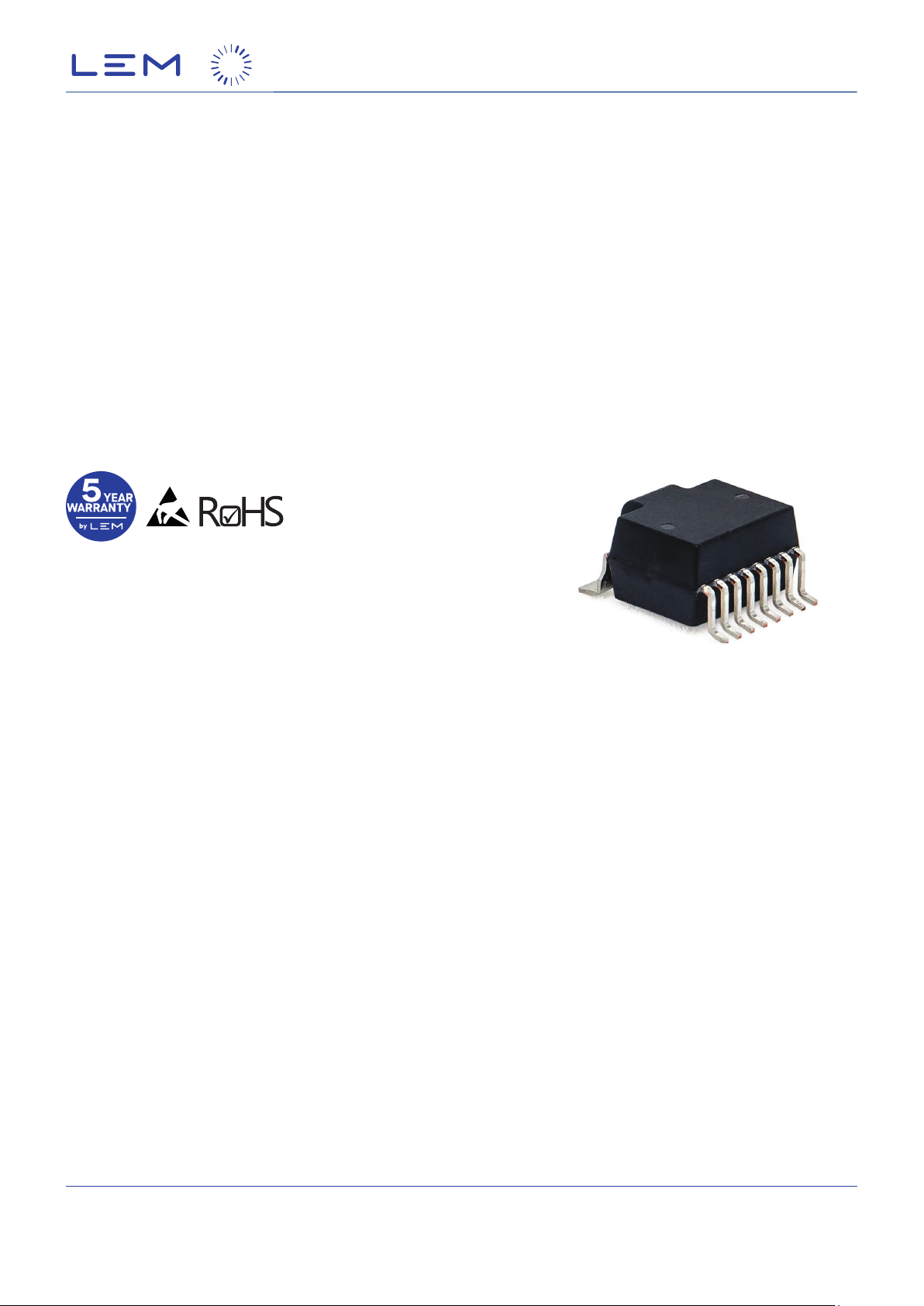
Integrated Current Sensor HMSR-SMS series I
= 6 ... 30 A
P N
Ref: HMSR 6-SMS, HMSR 8-SMS, HMSR 10-SMS, HMSR 15-SMS,
HMSR 20-SMS, HMSR 30-SMS
Denition
The HMSR is a new generation of high insulated Integrated Current Sensor from LEM.
These product family provides a robust, compact and very accurate solution for measuring DC and AC currents in all highly
demanding, switching power applications for commercial, industrial. HMSR is a micro core based open loop sensor with a
reinforced insulation and overcurrent detections (user congurable and factory set). These features make the device suitable for
high voltage applications requiring high precision and strong immunity against external eld.
The primary conductor (pins 1 and 8) has very low electrical resistance and dedicated pads designed to withstand against high
surge currents such as lightning strikes.
HMSR is measuring the magnetic eld generated by the current owing in the copper primary path of the device. By using a micro
magnetic core, HMSR is immune to the external elds, making the device well suited for power electronic applications with high
levels of disturbance.
The reinforced isolation between primary (pins 1 and 8) and secondary (pins 9 to 15) offers the HSMR, a small, cost effective
solution to measure high side current compared to resistive isolated solutions.
Features
● Open loop multi-range current transducer
● Voltage output
● Double overcurrent detection
● Single power supply +5 V
● Galvanic separation between primary and secondary
● Low power consumption
● Compact design for surface mount PCB mounting
● Factory calibrated
● High bandwidth, very low loss magnetic core.
Advantages
● Low prole: h = 6 mm
● Small foot-print
● Low electrical resistance 0.76 mΩ
● Reinforced insulation capability
● High resolution
● High immunity to external interference
● Lightning impulse current ≤ 20 kA.
Applications
● Small drives
● HVAC Inverters
● Appliances
● Solar Inverters.
Standards
● IEC 61800-5-1: 2007
● IEC 62109-1: 2010
● IEC 60950-1: 2005
● UL 1577: 2014 (pending).
Application Domains
● Industrial
● Automotive (pending).
N°97.T4.09.000.0; N°97.T4.11.000.0; N°97.T4.13.000.0; N°97.T4.15.000.0 ; N°97.T4.17.000.0; N°97.T4.23.000.0
18June2020/version 3
LEM reserves the right to carry out modications on its transducers,
in order to improve them, without prior notice
LEM International SA
Chemin des Aulx 8
1228 PLAN-LES-OUATES Switzerland
www.lem.com
Page 1/17
Page 2
HMSR-SMS series
Safety
⚠
Caution
If the device is used in a way that is not specied by the manufacturer, the protection provided by the device may be compromised.
Always inspect the electronics unit and connecting cable before using this product and do not use it if damaged.
Mounting assembly shall guarantee the maximum primary conductor temperature, fulll clearance and creepage distance,
minimize electric and magnetic coupling, and unless otherwise specied can be mounted in any orientation.
Caution, risk of electrical shock
This transducer must be used in limited-energy secondary circuits SELV according to IEC 61010-1, in electric/electronic equipment
with respect to applicable standards and safety requirements in accordance with the manufacturer’s operating specications.
Use caution during installation and use of this product; certain parts of the module can carry hazardous voltages and high currents
(e.g. power supply, primary conductor).
Ignoring this warning can lead to injury and or/or cause serious damage.
De-energize all circuits and hazardous live parts before installing the product.
All installations, maintenance, servicing operations and use must be carried out by trained and qualied personnel practicing
applicable safety precautions.
This transducer is a build-in device, whose hazardous live parts must be inaccessible after installation.
This transducer must be mounted in a suitable end-enclosure.
Main supply must be able to be disconnected.
This transducer is a built-in device, not intended to be cleaned with any product. Nevertheless if the user must implement cleaning
or washing process, validation of the cleaning program has to be done by the user in accordance with semi-conductor practices.
ESD susceptibility
The product is susceptible to be damaged from an ESD event and the personnel and work space should be grounded when
handling it.
Do not dispose of this product as unsorted municipal waste. Contact a qualied recycler for disposal.
Although LEM applies utmost care to facilitate compliance of end products with applicable regulations during LEM product
design, use of this part may need additional measures on the application side for compliance with regulations regarding EMC and
protection against electric shock. Therefore LEM cannot be held liable for any potential hazards, damages, injuries or loss of life
resulting from the use of this product.
18June2020/version 3
LEM reserves the right to carry out modications on its transducers,
in order to improve them, without prior notice
LEM International SA
Chemin des Aulx 8
1228 PLAN-LES-OUATES Switzerland
www.lem.com
Page 2/17
Page 3
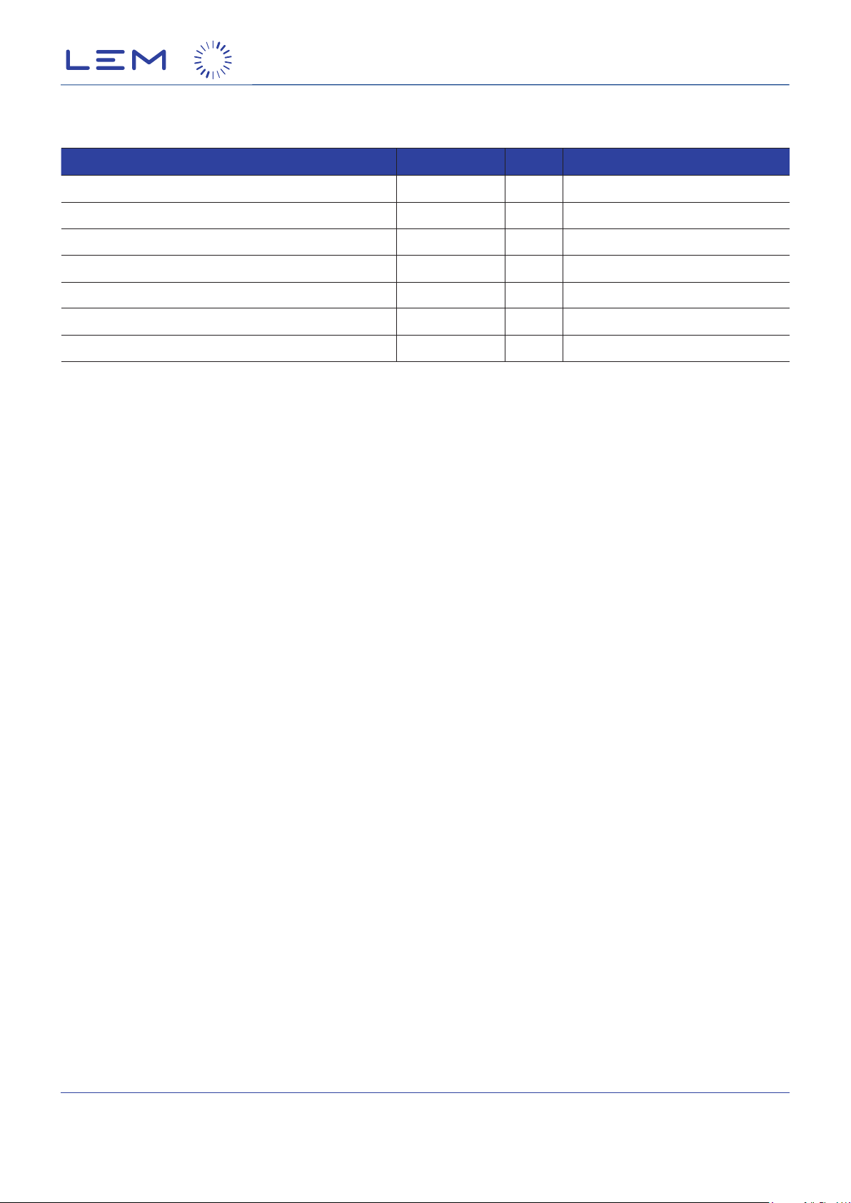
Absolute maximum ratings
Parameter Symbol Unit Value
HMSR-SMS series
Maximum supply voltage UC
Maximum supply voltage (working) (−40 … 125 °C) U
Electrostatic discharge voltage (HBM - Human Body Model) U
Electrostatic discharge voltage (CDM - Charged Device Model) U
Maximum output current source I
Maximum input current sink I
Maximum junction temperature T
max
C max
ESD HBM
ESD CDM
out max
in max
J max
mA 25
mA 50
Absolute maximum ratings apply at 25 °C unless otherwise noted.
Stresses above these ratings may cause permanent damage.
Exposure to absolute maximum ratings for extended periods may degrade reliability.
V 8
V 6.5
kV 2
V 500
°C 150
18June2020/version 3
LEM reserves the right to carry out modications on its transducers,
in order to improve them, without prior notice
LEM International SA
Chemin des Aulx 8
1228 PLAN-LES-OUATES Switzerland
www.lem.com
Page 3/17
Page 4
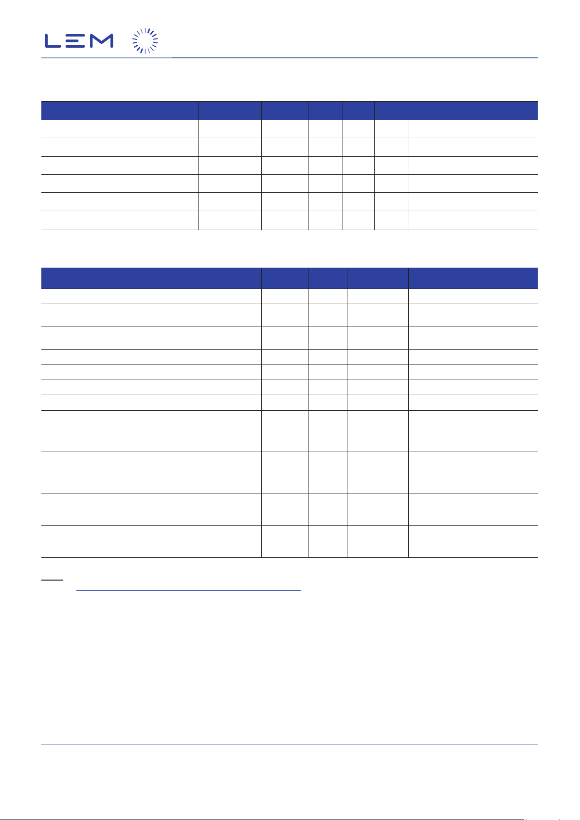
Environmental and mechanical characteristics
HMSR-SMS series
Parameter Symbol Unit Min
Ambient operating temperature T
Ambient storage temperature T
T
Resistance of the primary @
Thermal resistance junction to case
Thermal resistance junction to ambient
Mass
= 25 °C
A
1)
1)
R
R
R
th JC
th JA
m
A
A st
P
°C −40 125
°C −55 165
mΩ 0.76
K/W 18
K/W 19
g 1.4
Typ Max Comment
Insulation coordination
Parameter Symbol Unit ≤ Value
RMS voltage for AC insulation test, 50 Hz, 1 min U
Impulse withstand voltage 1.2/50 μs U
Partial discharge RMS test voltage (
q
< 5 pC) U
m
Clearance (pri. - sec.) d
Creepage distance (pri. - sec.) d
d
Ni
t
CI
Cp
Case material - - V0 According to UL 94, amability
Comparative tracking index
CTI
Application example
System voltage RMS
Application example
System voltage RMS
Application example
System voltage DC
Application example
System voltage DC
kV 4.95 According to IEC 60950-1
kV 8
V 1650
According to IEC 62109-1,
IEC 61800-5-1
According to IEC 62109-1,
IEC 61800-5-1
mm 8 Shortest distance through air
mm 8 Shortest path along device body
600 grade requirements mas compand
Basic insulation according to
V 1000
IEC 61800-5-1, IEC 62109-1,
IEC 60950-1
CAT III, PD2
Reinforced insulation according to
V 600
IEC 61800-5-1, IEC 62109-1,
IEC 60950-1
CAT III, PD2
Basic insulation according to
V 1500
IEC 62109-1
CAT III, PD2
Reinforced insulation according to
V 800
IEC 62109-1
CAT III, PD2
Comment
Note: 1) Done on LEM evaluation board PCB 6030:
https://www.lem.com/en/hmsr-miniature-current-sensors.
18June2020/version 3
LEM reserves the right to carry out modications on its transducers,
in order to improve them, without prior notice
LEM International SA
Chemin des Aulx 8
1228 PLAN-LES-OUATES Switzerland
www.lem.com
Page 4/17
Page 5
HMSR-SMS series
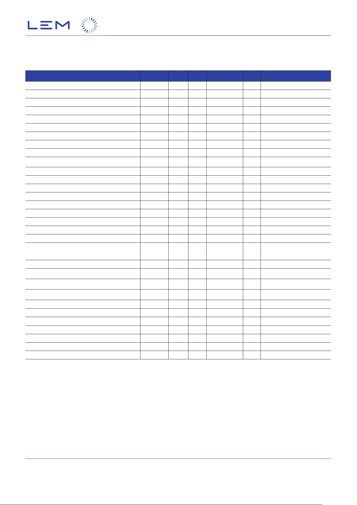
Electrical data HMSR 6-SMS
At TA = 25 °C, UC = 5 V, RL = 10 kΩ, unless otherwise noted (see Min, Max, typ, denition paragraph in page 11).
Parameter Symbol Unit Min
Primary nominal current I
Primary current, measuring range I
Internal reference voltage @
Output voltage range @
Output Internal resistance of
Output Internal resistance of
Load capacitance on
Load capacitance on
DC supply voltage ⎓ U
DC current consumption ⎓ I
Nominal sensitivity S
Sensitivity error ε
Sum of sensitivity and linearity error @
Electrical offset voltage referred to primary U
Electrical offset current referred to primary I
Temperature coefcient of
Temperature coefcient of
Temperature coefcient of
Temperature coefcient of
Magnetic offset current after overload (
referred to primary
Noise voltage spectral density referred to primary u
Internal OCD detection threshold I
Internal OCD threshold error ε
Internal OCD output on resistance R
Linearity error 0 ... ±
I
Linearity error 0 ... ±I
Delay time @ 10 % of the nal output value I
Delay time @ 90 % of the nal output value
Internal OCD delay time t
Frequency bandwidth (−3 dB)
Internal OCD output hold time t
I
= 0 A U
P
I
P M
U
out
U
ref
U
out
U
ref
T
= 25 °C ε
A
S
U
I ref
U
O E
I
referred to primary TCI
O E
I
> 500 A)
P
P N
P M
P N
I
P N
U
TCU
TCU
step t
step t
out
TCS
I OCD Th
I OCD Th
on I OCD
D I OCD
hold I OCD
P N
P M
I ref
− U
R
out
R
ref
C
C
C
N
S
S L 25
O E
O E
I
O M
no
ε
ε
D 10
D 90
BW
Typ Max Comment
A 6
A −15 15 With ±UC ≥ 4.6 V
V 2.48 2.5 2.52
V −2 2
ref
Ω 2 5
Ω 120 200 333
L
L
C
I ref
O E
O E
L
L
nF 0 4.7 6
nF 0 47 100
V 4.5 5 5.5
mA 20 26
mV/A 133.33 800 mV @ I
% −0.75 0.75 Factory adjustment
% of I
−1.5 1.5
P N
mV −5 5 U
mA −37.5 37.5
ppm/K −220 220 −40 °C ... 125 °C
ppm/K −150 150 −40 °C ... 125 °C
mV/K −0.1 0.1 −40 °C ... 125 °C
mA/K −0.56 0.56 −40 °C ... 125 °C
A 0.18
1/2
µV/Hz
14.8 100 Hz ... 100 kHz
A 2.75 x I
P N
% ±10 Referred to I
Ω 70 95 100 Open drain output, active low
% −0.75 0.75 Referred to I
% −0.5 0.5 Referred to I
µs 1.5
µs 2
µs 1.4 1.7 2.1
kHz 300
µs 7 10 14
P N
@ U
out − UI ref
25 °C ... 125 °C
P N
P N
P M
= 2.5 V
I ref
18June2020/version 3
LEM reserves the right to carry out modications on its transducers,
in order to improve them, without prior notice
LEM International SA
Chemin des Aulx 8
1228 PLAN-LES-OUATES Switzerland
www.lem.com
Page 5/17
Page 6
HMSR-SMS series
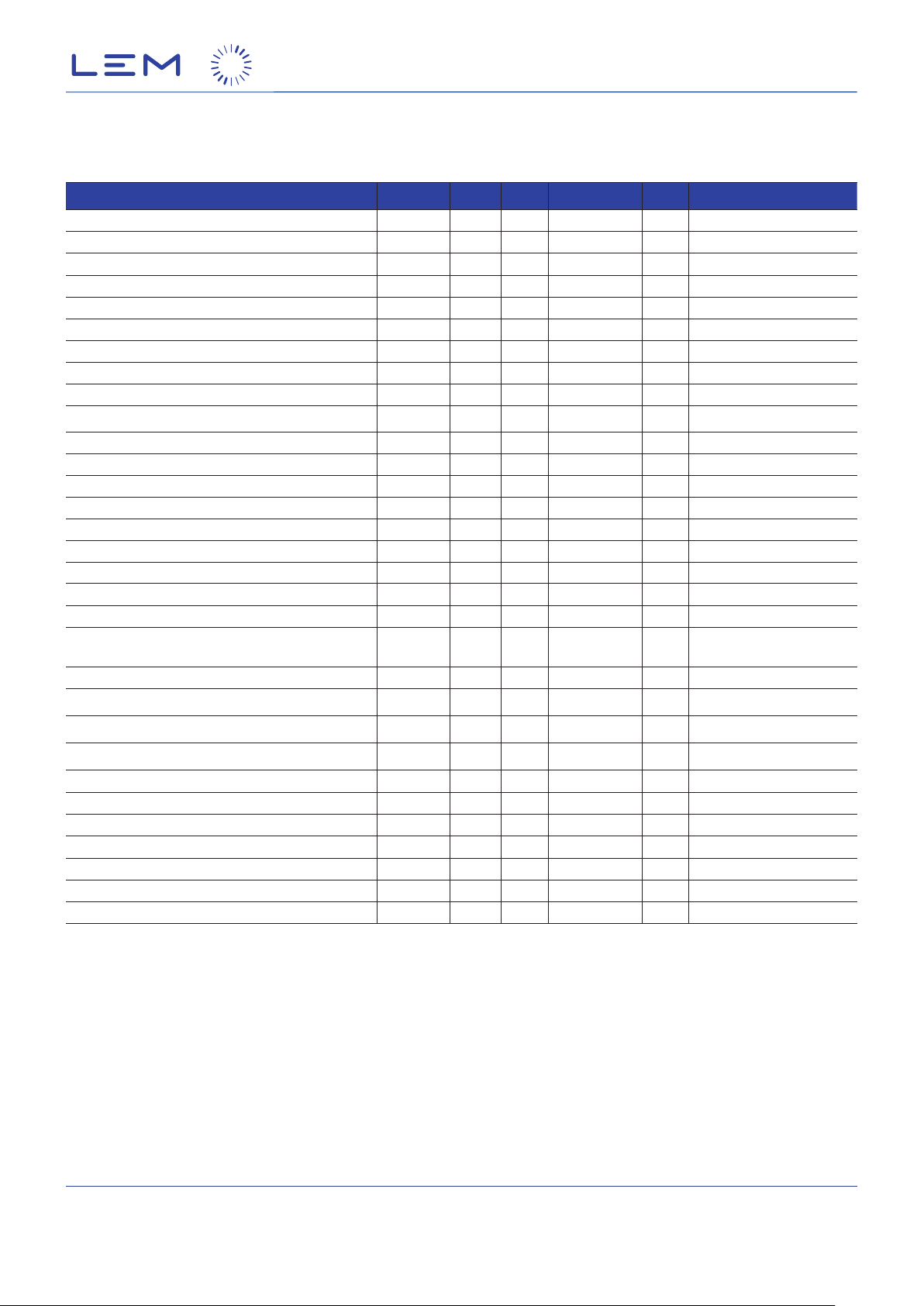
Electrical data HMSR 8-SMS
At TA = 25 °C, UC = 5 V, RL = 10 kΩ, unless otherwise noted (see Min, Max, typ, denition paragraph in page 11).
Parameter Symbol Unit Min
Primary nominal current I
Primary current, measuring range I
Internal reference voltage @
Output voltage range @
Output Internal resistance of
Output Internal resistance of
Load capacitance on
Load capacitance on
DC supply voltage ⎓ U
DC current consumption ⎓ I
Nominal sensitivity S
Sensitivity error ε
Sum of sensitivity and linearity error @
Electrical offset voltage referred to primary U
Electrical offset current referred to primary I
Temperature coefcient of
Temperature coefcient of
Temperature coefcient of
Temperature coefcient of
Magnetic offset current after overload (
referred to primary
Noise voltage spectral density referred to primary u
Internal OCD detection threshold I
Internal OCD threshold error ε
Internal OCD output on resistance R
Linearity error 0 ... ±
I
Linearity error 0 ... ±I
Delay time to 10 % of the nal output value for I
Delay time @ 90 % of the nal output value for
Internal OCD delay time t
Frequency bandwidth (−3 dB)
Internal OCD output hold time t
I
= 0 A U
P
I
P M
U
out
U
ref
U
out
U
ref
T
= 25 °C ε
A
S
U
I ref
U
O E
I
referred to primary TCI
O E
I
> 500 A)
P
P N
P M
P N
I
P N
U
step t
step t
out
TCS
TCU
TCU
I OCD Th
I OCD Th
on I OCD
D I OCD
hold I OCD
P N
P M
I ref
− U
R
out
R
C
C
S L 25
O E
O E
I
O M
no
ε
ε
D 10
D 90
BW
Typ Max Comment
A 8
A −20 20 With ±UC ≥ 4.6 V
V 2.48 2.5 2.52
V −2 2
ref
Ω 2 5
ref
L
L
C
C
N
S
I ref
O E
O E
L
L
Ω 120 200 333
nF 0 4.7 6
nF 0 47 100
V 4.5 5 5.5
mA 20 26
mV/A 100 800 mV @ I
% −0.75 0.75 Factory adjustment
% of I
−1.5 1.5
P N
mV −5 5 U
mA −50 50
ppm/K −200 200 −40 °C ... 125 °C
ppm/K −150 150 −40 °C ... 125 °C
mV/K −0.1 0.1 −40 °C ... 125 °C
mA/K −0.75 0.75 −40 °C ... 125 °C
A 0.18
1/2
µV/Hz
12.2 100 Hz ... 100 kHz
A 2.75 x I
P N
% ±10 Referred to I
Ω 70 95 100 Open drain output, active low
% −0.75 0.75 Referred to I
% −0.5 0.5 Referred to I
µs 1.5
µs 2
µs 1.4 1.7 2.1
kHz 300
µs 7 10 14
P N
@ U
out − UI ref
25 °C ... 125 °C
P N
P N
P M
= 2.5 V
I ref
18June2020/version 3
LEM reserves the right to carry out modications on its transducers,
in order to improve them, without prior notice
LEM International SA
Chemin des Aulx 8
1228 PLAN-LES-OUATES Switzerland
www.lem.com
Page 6/17
Page 7
HMSR-SMS series
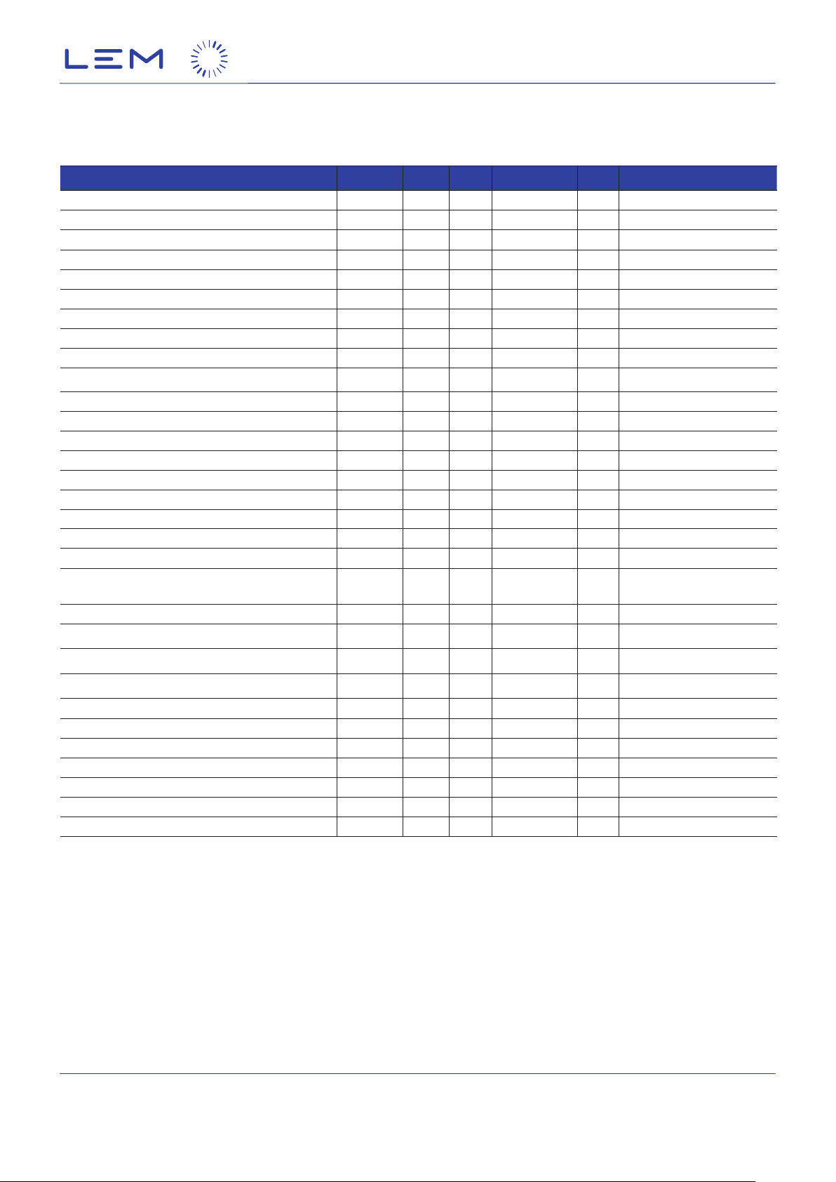
Electrical data HMSR 10-SMS
At TA = 25 °C, UC = 5 V, RL = 10 kΩ, unless otherwise noted (see Min, Max, typ, denition paragraph in page 11).
Parameter Symbol Unit Min
Primary nominal current I
Primary current, measuring range I
Internal reference voltage @
Output voltage range @
Output Internal resistance of
Output Internal resistance of
Load capacitance on
Load capacitance on
DC supply voltage ⎓ U
DC current consumption ⎓ I
Nominal sensitivity S
Sensitivity error ε
Sum of sensitivity and linearity error @
Electrical offset voltage referred to primary U
Electrical offset current referred to primary I
Temperature coefcient of
Temperature coefcient of
Temperature coefcient of
Temperature coefcient of
Magnetic offset current after overload (
referred to primary
Noise voltage spectral density referred to primary u
Internal OCD detection threshold I
Internal OCD threshold error ε
Internal OCD output on resistance R
Linearity error 0 ... ±
I
Linearity error 0 ... ±I
Delay time @ 10 % of the nal output value I
Delay time @ 90 % of the nal output value
Internal OCD delay time t
Frequency bandwidth (−3 dB)
Internal OCD output hold time t
I
= 0 A U
P
I
P M
U
out
U
ref
U
out
U
ref
T
= 25 °C ε
A
S
U
I ref
U
O E
I
referred to primary TCI
O E
I
> 500 A)
P
P N
P M
step t
P N
I
step t
P N
U
out
TCU
TCU
I OCD Th
I OCD Th
on I OCD
hold I OCD
TCS
D I OCD
P N
P M
I ref
− U
R
out
R
C
C
S L 25
O E
O E
I
O M
ε
ε
D 10
D 90
BW
Typ Max Comment
A 10
A −25 25 With ±UC ≥ 4.6 V
V 2.48 2.5 2.52
V −2 2
ref
Ω 2 5
ref
L
L
C
C
N
S
I ref
O E
O E
no
L
L
Ω 120 200 333
nF 0 4.7 6
nF 0 47 100
V 4.5 5 5.5
mA 20 26
mV/A 80 800 mV @ I
% −0.75 0.75 Factory adjustment
% of I
−1.25 1.25
P N
mV −5 5 U
mA −62.5 62.5
ppm/K −200 200 −40 °C ... 125 °C
ppm/K −150 150 −40 °C ... 125 °C
mV/K −0.075 0.075 −40 °C ... 125 °C
mA/K −0.94 0.94 −40 °C ... 125 °C
A 0.18
1/2
µV/Hz
8.6 100 Hz ... 100 kHz
A 2.75 x I
P N
% ±10 Referred to I
Ω 70 95 100 Open drain output, active low
% −0.5 0.5 Referred to I
% −0.5 0.5 Referred to I
µs 1.5
µs 2
µs 1.4 1.7 2.1
kHz 300
µs 7 10 14
P N
out − UI ref
@ U
25 °C ... 125 °C
P N
P N
P M
= 2.5 V
I ref
18June2020/version 3
LEM reserves the right to carry out modications on its transducers,
in order to improve them, without prior notice
LEM International SA
Chemin des Aulx 8
1228 PLAN-LES-OUATES Switzerland
www.lem.com
Page 7/17
Page 8
HMSR-SMS series
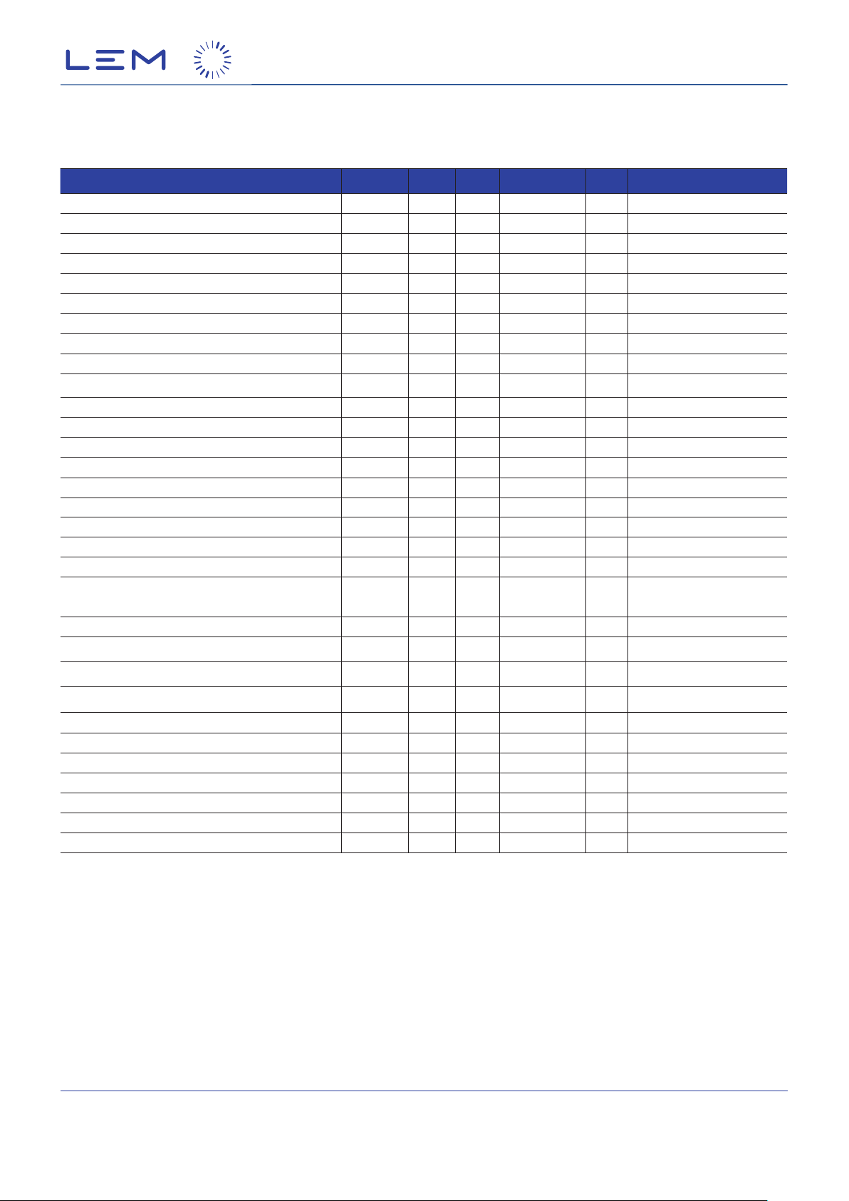
Electrical data HMSR 15-SMS
At TA = 25 °C, UC = 5 V, RL = 10 kΩ, unless otherwise noted (see Min, Max, typ, denition paragraph in page 11).
Parameter Symbol Unit Min
Primary nominal current I
Primary current, measuring range I
Internal reference voltage @
Output voltage range @
Output Internal resistance of
Output Internal resistance of
Load capacitance on
Load capacitance on
DC supply voltage ⎓ U
DC current consumption ⎓ I
Nominal sensitivity S
Sensitivity error ε
Sum of sensitivity and linearity error @
Electrical offset voltage referred to primary U
Electrical offset current referred to primary I
Temperature coefcient of
Temperature coefcient of
Temperature coefcient of
Temperature coefcient of
Magnetic offset current after overload (
referred to primary
Noise voltage spectral density referred to primary u
Internal OCD detection threshold I
Internal OCD threshold error ε
Internal OCD output on resistance R
Linearity error 0 ... ±
I
Linearity error 0 ... ±I
Delay time @ 10 % of the nal output value I
Delay time @ 90 % of the nal output value
Internal OCD delay time t
Frequency bandwidth (−3 dB)
Internal OCD output hold time t
I
= 0 A U
P
I
P M
U
out
U
ref
U
out
U
ref
T
= 25 °C ε
A
S
U
I ref
U
O E
I
referred to primary TCI
O E
I
> 500 A)
P
P N
P M
step t
P N
I
step t
P N
U
out
TCS
TCU
TCU
I OCD Th
I OCD Th
on I OCD
D I OCD
hold I OCD
P N
P M
I ref
− U
R
out
R
ref
C
C
C
S L 25
O E
O E
I
O M
no
ε
ε
D 10
D 90
BW
Typ Max Comment
A 15
A −37.5 37.5 With ±UC ≥ 4.6 V
V 2.48 2.5 2.52
V −2 2
ref
Ω 2 5
Ω 120 200 333
L
L
C
N
S
I ref
O E
O E
L
L
nF 0 4.7 6
nF 0 47 100
V 4.5 5 5.5
mA 20 26
mV/A 53.33 800 mV @ I
% −0.75 0.75 Factory adjustment
% of I
−1.25 1.25
P N
mV −5 5 U
mA −93.75 93.75
ppm/K −200 200 −40 °C ... 125 °C
ppm/K −150 150 −40 °C ... 125 °C
mV/K −0.075 0.075 −40 °C ... 125 °C
mA/K −1.41 1.41 −40 °C ... 125 °C
A 0.18
1/2
µV/Hz
6.3 100 Hz ... 100 kHz
A 2.75 x I
P N
% ±10 Referred to I
Ω 70 95 100 Open drain output, active low
% −0.5 0.5 Referred to I
% −0.5 0.5 Referred to I
µs 1.5
µs 2
µs 1.4 1.7 2.1
kHz 300
µs 7 10 14
P N
@ U
out − UI ref
25 °C ... 125 °C
P N
P N
P M
= 2.5 V
I ref
18June2020/version 3
LEM reserves the right to carry out modications on its transducers,
in order to improve them, without prior notice
LEM International SA
Chemin des Aulx 8
1228 PLAN-LES-OUATES Switzerland
www.lem.com
Page 8/17
Page 9
HMSR-SMS series
Electrical data HMSR 20-SMS
At TA = 25 °C, UC = 5 V, RL = 10 kΩ, unless otherwise noted (see Min, Max, typ, denition paragraph in page 11).
Parameter Symbol Unit Min
Primary nominal current I
Primary current, measuring range I
Internal reference voltage @
Output voltage range @
Output Internal resistance of
Output Internal resistance of
Load capacitance on
Load capacitance on
DC supply voltage ⎓ U
DC current consumption ⎓ I
Nominal sensitivity S
Sensitivity error ε
Sum of sensitivity and linearity error @
Electrical offset voltage referred to primary U
Electrical offset current referred to primary I
Temperature coefcient of
Temperature coefcient of
Temperature coefcient of
Temperature coefcient of
Magnetic offset current after overload (
referred to primary
Noise voltage spectral density referred to primary u
Internal OCD detection threshold I
Internal OCD threshold error ε
Internal OCD output on resistance R
Linearity error 0 ... ±
I
Linearity error 0 ... ±I
Delay time @ 10 % of the nal output value I
Delay time @ 90 % of the nal output value
Internal OCD delay time t
Frequency bandwidth (−3 dB)
Internal OCD output hold time t
I
= 0 A U
P
I
P M
U
out
U
ref
U
out
U
ref
T
= 25 °C ε
A
S
U
I ref
U
O E
I
referred to primary TCI
O E
I
> 500 A)
P
P N
P M
step t
P N
I
step t
P N
U
out
TCS
TCU
TCU
I OCD Th
I OCD Th
on I OCD
D I OCD
hold I OCD
P N
P M
I ref
− U
R
out
R
ref
C
C
C
S L 25
O E
O E
I
O M
no
ε
ε
D 10
D 90
BW
Typ Max Comment
A 20
A −50 50 With ±UC ≥ 4.6 V
V 2.48 2.5 2.52
V −2 2
ref
Ω 2 5
Ω 120 200 333
L
L
C
N
S
I ref
O E
O E
L
L
nF 0 4.7 6
nF 0 47 100
V 4.5 5 5.5
mA 20 26
mV/A 40 800 mV @ I
% −0.75 0.75 Factory adjustment
% of I
−1.25 1.25
P N
mV −5 5 U
mA −125 125
ppm/K −200 200 −40 °C ... 125 °C
ppm/K −150 150 −40 °C ... 125 °C
mV/K −0.075 0.075 −40 °C ... 125 °C
mA/K −1.88 1.88 −40 °C ... 125 °C
A 0.18
1/2
µV/Hz
4.5 100 Hz ... 100 kHz
A 2.75 x I
P N
% ±10 Referred to I
Ω 70 95 100 Open drain output, active low
% −0.5 0.5 Referred to I
% −0.5 0.5 Referred to I
µs 1.5
µs 2
µs 1.4 1.7 2.1
kHz 300
µs 7 10 14
P N
@ U
out − UI ref
25 °C ... 125 °C
P N
P N
P M
= 2.5 V
I ref
18June2020/version 3
LEM reserves the right to carry out modications on its transducers,
in order to improve them, without prior notice
LEM International SA
Chemin des Aulx 8
1228 PLAN-LES-OUATES Switzerland
www.lem.com
Page 9/17
Page 10
HMSR-SMS series
Electrical data HMSR 30-SMS
At TA = 25 °C, UC = 5 V, RL = 10 kΩ, unless otherwise noted (see Min, Max, typ, denition paragraph in page 11).
Parameter Symbol Unit Min
Primary nominal current I
Primary current, measuring range I
Internal reference voltage @ IP = 0 A U
Output voltage range @
Output Internal resistance of
Output Internal resistance of
Load capacitance on
Load capacitance on
DC supply voltage ⎓ U
DC current consumption ⎓ I
Nominal sensitivity S
Sensitivity error ε
Sum of sensitivity and linearity error @
Electrical offset voltage referred to primary U
Electrical offset current referred to primary I
Temperature coefcient of
Temperature coefcient of
Temperature coefcient of
Temperature coefcient of
Magnetic offset current after overload (
referred to primary
Noise voltage spectral density referred to primary u
Internal OCD detection threshold I
Internal OCD threshold error ε
Internal OCD output on resistance R
Linearity error 0 ... ±
Linearity error 0 ... ±I
Delay time @ 10 % of the nal output value I
Delay time @ 90 % of the nal output value
Internal OCD delay time t
Frequency bandwidth (−3 dB)
Internal OCD output hold time t
I
P M
U
out
U
ref
U
out
U
ref
T
= 25 °C ε
A
S
U
I ref
U
O E
I
referred to primary TCI
O E
I
> 500 A)
P
I
P N
P M
step t
P N
I
step t
P N
U
out
TCU
TCU
I OCD Th
I OCD Th
on I OCD
D I OCD
hold I OCD
TCS
P N
P M
I ref
− U
R
out
R
ref
C
C
C
S L 25
O E
O E
I
O M
no
ε
ε
D 10
D 90
BW
Typ Max Comment
A 30
A −75 75 With ±UC ≥ 4.6 V, TA < 75 °C
V 2.48 2.5 2.52
V −2 2
ref
Ω 2 5
Ω 120 200 333
L
L
C
N
S
I ref
O E
O E
L
L
nF 0 4.7 6
nF 0 47 100
V 4.5 5 5.5
mA 20 26
mV/A 26.67 800 mV @ I
% −0.75 0.75 Factory adjustment
% of I
−1.25 1.25
P N
mV −5 5 U
mA −187.5 187.5
ppm/K −200 200 −40 °C ... 125 °C
ppm/K −150 150 −40 °C ... 125 °C
mV/K −0.075 0.075 −40 °C ... 125 °C
mA/K −2.81 2.81 −40 °C ... 125 °C
A 0.18
1/2
µV/Hz
3.2 100 Hz ... 100 kHz
A 2.75 x I
P N
% ±10 Referred to I
Ω 70 95 100 Open drain output, active low
% −0.5 0.5 Referred to I
% −0.5 0.5 Referred to I
µs 1.5
µs 2
µs 1.4 1.7 2.1
kHz 300
µs 7 10 14
P N
@ U
out − UI ref
25 °C ... 125 °C
P N
P N
P M
= 2.5 V
I ref
1)
Note: 1) See gure 2.
18June2020/version 3
LEM reserves the right to carry out modications on its transducers,
in order to improve them, without prior notice
LEM International SA
Chemin des Aulx 8
1228 PLAN-LES-OUATES Switzerland
www.lem.com
Page 10/17
Page 11
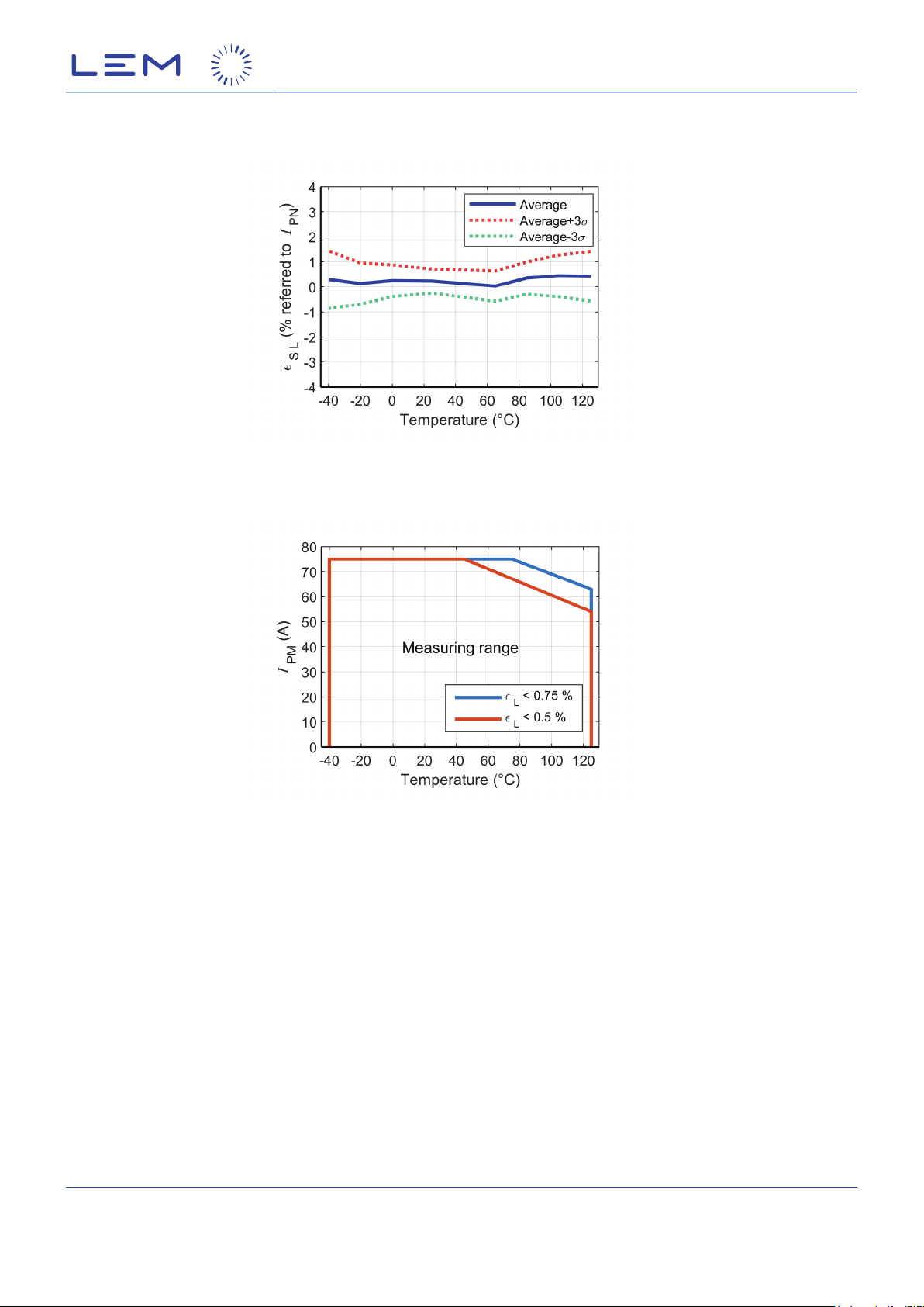
Sum of sensitivity and linearity error
Figure 1: Typical value on HMSR 20-SMS (40 parts)
Measuring range vs ambient temperature
HMSR-SMS series
Figure 2
Denition of typical, minimum and maximum values
Minimum and maximum values for specied limiting and safety conditions have to be understood as such as well as values shown
in “typical” graphs.
On the other hand, measured values are part of a statistical distribution that can be specied by an interval with upper and lower
limits and a probability for measured values to lie within this interval.
Unless otherwise stated (e.g. “100 % tested”), the LEM denition for such intervals designated with “min” and “max” is that the
probability for values of samples to lie in this interval is 99.73 %.
For a normal (Gaussian) distribution, this corresponds to an interval between −3 sigma and +3 sigma. If “typical” values are not
obviously mean or average values, those values are dened to delimit intervals with a probability of 68.27 %, corresponding to an
interval between −sigma and +sigma for a normal distribution.
Typical, maximal and minimal values are determined during the initial characterization of the product.
Page 11/17
18June2020/version 3
LEM reserves the right to carry out modications on its transducers,
in order to improve them, without prior notice
LEM International SA
Chemin des Aulx 8
1228 PLAN-LES-OUATES Switzerland
www.lem.com
Page 12
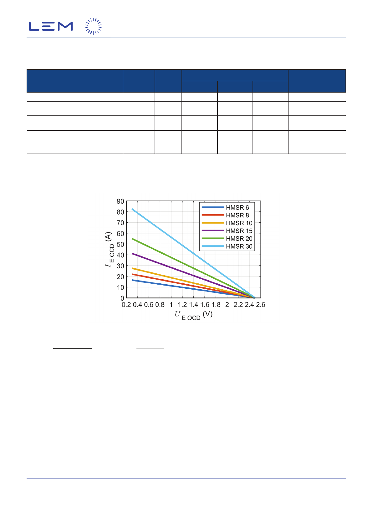
External overcurrent detection
R
N
UU
−
HMSR-SMS series
Parameter Symbol Unit
External OCD voltage
External OCD output on resistance to
ground
External OCD delay time
External OCD output hold time
External OCD threshold error
I
: External overcurrent detection (OCD threshold) at U
E OCD
U
E OCD
R
on E OCD
t
D E OCD
t
hold E OCD
ε
E OCD
V 0.3 2.5
Ω 35 200 300
µs 7 10 13
µs 7 10 14
% ±6
Specication
Min Typical Max
= 2.5 V
ref
Conditions
Open drain output,
active low
To be added to the
sensor delay time
Referred to
I
P N
E OCD
=
I
18June2020/version 3
ref E OCD
S
U
= ×
E OCD ref
LEM reserves the right to carry out modications on its transducers,
in order to improve them, without prior notice
E
RR
+
E ref
U
Figure 3
with 0.3 ≤ U
E OCD
≤ U
ref
LEM International SA
Chemin des Aulx 8
1228 PLAN-LES-OUATES Switzerland
www.lem.com
Page 12/17
Page 13
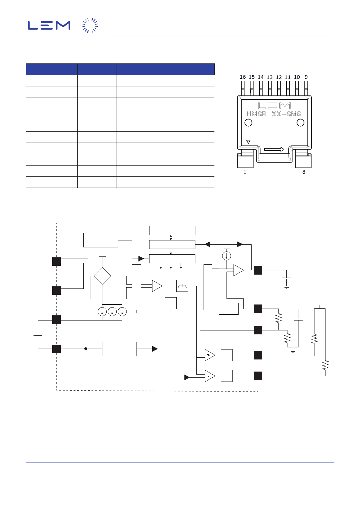
Pins denition
Pins number Name Description
1 IP+ Input of the primary current
HMSR-SMS series
8
9 OCD INT Internal OCD
10
11
12
13 NC No internal connection
14 OCD EXT External OCD terminal
15 GND Ground terminal
16
Block diagram
IP+
Magnetic
Core
IP−
U
C
U
ref
U
out
U
E OCD
Thermometer
8x
Output of the primary current
Supply voltage
Reference voltage
Output voltage
External OCD threshold voltage terminal
EEPROM Memory
Digital Interface
DAC’s
Hall
Cells
Corrections
Filter
Single Wire Bus Interface
Offset
Correction
Filter Adjust
Figure 4
U
out
4.7 nF
I
-
P
GND
47 nF
U
C
18June2020/version 3
Bias
Sensitivity Correction
5 V
Sensitivity Adjust
SPINNING
Clock
Regulator
3.3 V
From DAC
Adjust Level
Figure 5
LEM reserves the right to carry out modications on its transducers,
in order to improve them, without prior notice
DEMODULATION
Voltage
Reference
Timer
Adjust Timeout
Timer
U
ref
R
ref
U
E OCD
R
E
OCD EXT
OCD INT
LEM International SA
Chemin des Aulx 8
1228 PLAN-LES-OUATES Switzerland
www.lem.com
47 nF
R
E OCD
R
I OCD
Page 13/17
U
C
Page 14
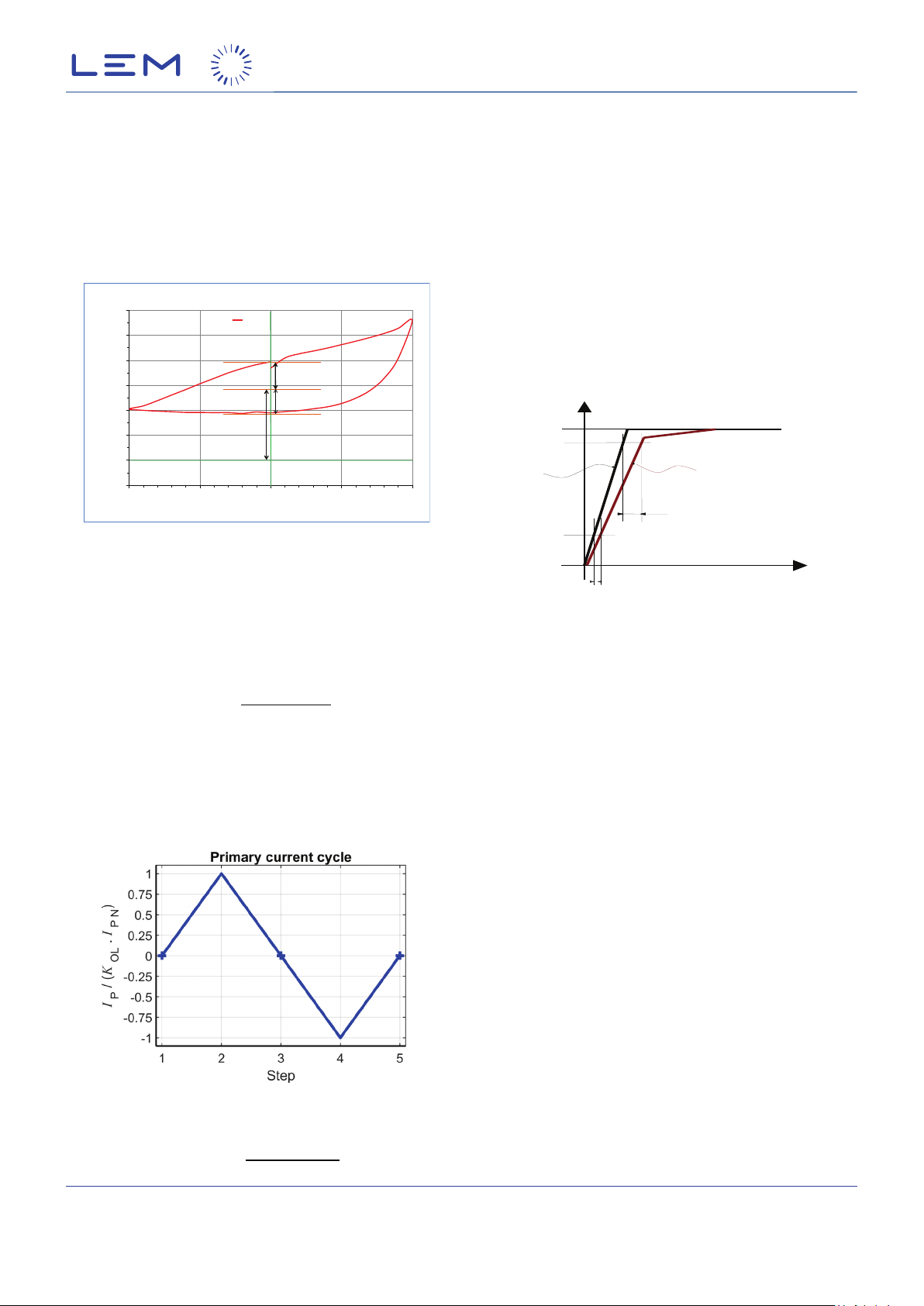
Total error referred to primary
ℇ
I
)
2
II
2
II
I
t
D 10
t
D 90
t
90 %
10 %
100
The total error ε
I
.
P N
It includes all errors mentioned above
● the electrical offset I
● the magnetic offset I
● the sensitivity error ε
● the linearity error εL (to I
0.12
0.10
0.08
P N
0.06
(%
0.04
tot
0.02
0.00
-0.02
-1 -0.5 0 0.5 1
is the error at ±I
tot
O E
O M
S
P N
Total error ℇ
at UC= ... V and TA= 25 °C
I
/ I
O E (max)
IP/ (KOL· I
P N
, relative to the rated value
P N
).
tot
av er. + 3 σ
I
O M (max)
=
) with KOL= 1 ... 10
P N
Terms and denitions
Sensitivity and linearity
To measure sensitivity and linearity, the primary current (DC) is
cycled from 0 to IP, then to −IP and back to 0 (equally spaced
I
P N
linear regression line for a cycle between ±I
The linearity error ε
difference between the measured points and the linear
regression line, expressed in % of I
Delay times
The delay time t
respect to the primary are shown in the next gure.
Both slightly depend on the primary current di/dt.
/ I
P N
They are measured at nominal current.
HMSR-SMS series
/10 steps). The sensitivity S is dened as the slope of the
.
is the maximum positive or negative
L
P N
@ 10 % and the delay time t
D 10
I
%
I
P
P N
.
@ 90 % with
D 90
S
Figure 6: Total error ε
tot
Electrical offset referred to primary
Using the current cycle shown in gure 7, the electrical offset
current I
input current is zero.
is the residual output referred to primary when the
O E
Magnetic offset referred to primary
I+=
O E
The magnetic offset current I
on the primary side (“memory effect” of the transducer’s ferromagnetic core). It is measured using the following primary
current cycle. I
KOL: Overload factor
depends on the current value IP ≥ I
O M
P (3) P (5)
is the consequence of a current
O M
.
P N
Figure 8: t
(delay time @ 10 %) and
D 10
t
(delay time @ 90 %).
D 90
Figure 7: Current cycle used to measure magnetic and
18June2020/version 3
electrical offset (transducer supplied)
I−=
O M
P (3) P (5)
LEM reserves the right to carry out modications on its transducers,
in order to improve them, without prior notice
LEM International SA
Chemin des Aulx 8
1228 PLAN-LES-OUATES Switzerland
www.lem.com
Page 14/17
Page 15
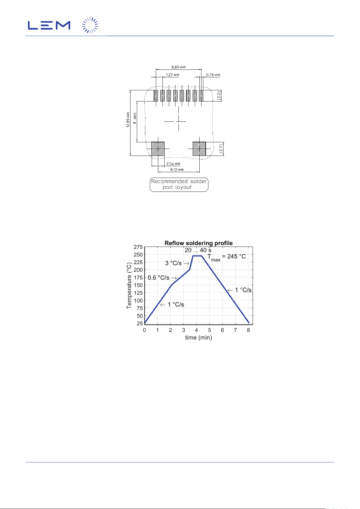
PCB footprint (in mm)
HMSR-SMS series
Figure 9
Soldering on PCB
Figure 10
Soldering remarks:
● HMSR is qualied MSL1 for storage and mounting purposes.
● Per JEDEC J-STD-020E for packages more than 2.5 mm thick per table 4.2 (Pb-Free Process) of the specication.
● Best practice is to use 7 zones or greater conventional reow system, limiting the time at reow temperature as indicated in
prole above.
● Rework not recommended.
18June2020/version 3
LEM reserves the right to carry out modications on its transducers,
in order to improve them, without prior notice
LEM International SA
Chemin des Aulx 8
1228 PLAN-LES-OUATES Switzerland
www.lem.com
Page 15/17
Page 16
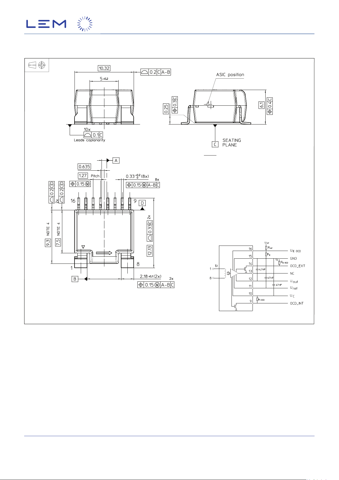
Dimensions (in mm)
HMSR-SMS series
NOTES:
1) MATERIALS:
Primary/Secondary: Copper
2) PLATING:
All terminals: Tin-Bismuth
3) CUSTOMER MOUNTING:
See PCB layout recommendation
4) NOTES:
Dimensions does not include mold ashes.
Protrusion or burrs shall not exceed 0.15 mm per ends.
Connection
Mechanical characteristics
● General tolerance ±0.15 mm
Remark
● U
− U
is positive when IP ows in the direction of arrow
out
ref
(pin 1 to pin 8).
18June2020/version 3
LEM reserves the right to carry out modications on its transducers,
in order to improve them, without prior notice
LEM International SA
Chemin des Aulx 8
1228 PLAN-LES-OUATES Switzerland
www.lem.com
Page 16/17
Page 17
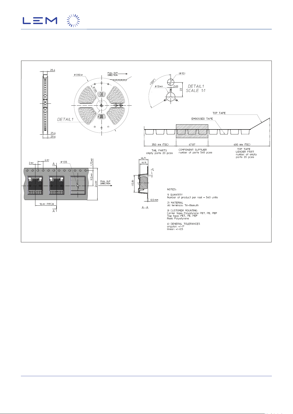
Tape and Reel (in mm)
HMSR-SMS series
18June2020/version 3
LEM reserves the right to carry out modications on its transducers,
in order to improve them, without prior notice
LEM International SA
Chemin des Aulx 8
1228 PLAN-LES-OUATES Switzerland
www.lem.com
Page 17/17
 Loading...