

Page 1
,QVWUXFWLRQ0DQXDO
/H&UR\$3
$FWLYH'LIIHUHQWLDO3UREH
REVISION D — JANUARY 2000
Page 2
Warranty
LeCroy warrants this oscilloscope accessory for normal use and operation within
specifications for a period of three years from the date of shipment. Calibration after each 12
month interval is recommended to ensure performance to specification. Spare parts,
replacement parts and repairs are warranted for 90 days. The instrument’s firmware has
been thoroughly tested and thought to be functional, but is supplied without warranty of any
kind covering detailed performance.
In exercising its warranty, LeCroy will repair or, at its option, replace any assembly returned
within its warranty period to the Customer Service Department or an authorized service
center. However, this will be done only if the product is determined by LeCroy’s examination
to be defective because of workmanship or materials, and the defect is not caused by misuse,
neglect, accident, abnormal conditions of operation, or damage resulting from attempted
repair or modifications by a non-authorized service facility.
The customer will be responsible for the transportation and insurance charges for the return of
products to the service facility. LeCroy will return all products under warranty with
transportation prepaid.
This warranty replaces all other warranties, expressed or implied, including but not lim ited to
any implied warranty of merchantability, fitness, or adequacy for any particular purposes or
use. LeCroy shall not be liable for any special, incidental, or consequential damages, whether
in contract or otherwise.
Corporate Headquarters
700 Chestnut Ridge Road
Chestnut Ridge, NY 10977-6499
Tel: (914) 578-6020, Fax: (914) 578-5985
Internet: www.lecroy.com
Copyright 2000, LeCroy Corporation. All rights reserved. Contents of this publication may not
be reproduced in any form without written permission of LeCroy Corporation.
LeCroy, Easywave, SMART Trigger, PowerMeasure, and ProBus are registered trademarks
of LeCroy Corporation.
AP034-OM-E Rev D 0100
Page 3

&RQWHQWV
Table of Contents
Overview
Description .................................................................................................................................. 1-1
Applications ................................................................................................................................. 1-1
Conventions used in this Manual ................................................................................................ 1-2
Safety Information
Operator Safety ........................................................................................................................... 2-1
Operation
Connecting the Probe to the Test Instrument ............................................................................. 3-1
Connecting the Probe to the Test Circuit ......................................................................................3-1
Probe Input Loading .................................................................................................................... 3-4
Grounding the Probe ................................................................................................................... 3-4
Selecting the Proper Range ........................................................................................................ 3-6
Operation with LeCroy Oscilloscopes ......................................................................................... 3-7
AP034 Use with the ADPPS Power Supply...................................................................................3-8
Adding Offset ............................................................................................................................ 3-10
Autobalance .............................................................................................................................. 3-11
Designing Test Fixtures for the AP033 Probe ........................................................................... 3-12
Reference Information
Differential Mode and Common Mode ........................................................................................ 4-1
Differential Mode Range and Common Mode Range...................................................................4-1
Common Mode Rejection Ratio ................................................................................................... 4-2
Care and Maintenance
Cleaning ...................................................................................................................................... 5-1
Calibration Interval ...................................................................................................................... 5-1
Service Strategy .......................................................................................................................... 5-1
Troubleshooting .......................................................................................................................... 5-1
Trace Off Scale................................................................................................................5-1
AP034-OM-E Rev D ISSUED: January 2000 LLL
Page 4

$3$FWLYH3UREH
Incorrect Frequency Response........................................................................................5-2
DC Errors.........................................................................................................................5-3
Poor Common Mode Rejection.......................................................................................5-3
Returning a Defective Probe ....................................................................................................... 5-4
Replacement Parts ...................................................................................................................... 5-5
Matching Procedure for ÷10 Plug-On External Attenuator .......................................................... 5-8
Equipment Required .....................................................................................................................5-8
Procedure......................................................................................................................................5-9
Performance Verification
Test Equipment Required .............................................................................................................6-1
Preliminary Procedure...................................................................................................................6-3
Procedure......................................................................................................................................6-3
Check Gain Accuracy.......................................................................................................6-4
Check High Frequency CMRR.........................................................................................6-5
Check Low Frequency CMRR..........................................................................................6-8
Performance Verification Test Record........................................................................................6-11
Adjustment Procedure
Introduction .................................................................................................................................. 7-1
Test Equipment Required .............................................................................................................7-2
Preliminary Procedure...................................................................................................................7-4
Procedure......................................................................................................................................7-7
Adjust Coarse DC Balance (R226) ..................................................................................7-7
Adjust Fine DC Balance (R304).......................................................................................7-8
Adjust Low Frequency CMRR (R7)..................................................................................7-9
Adjust Offset (R330) ......................................................................................................7-11
Adjust Gain (R322C)......................................................................................................7-13
Adjust Final Attenuator Compensation (C17) ................................................................7-14
Adjust Final Attenuator CMRR (C18A)...........................................................................7-15
Assemble Probe and Amplifier.......................................................................................7-16
Attenuator Matching and Final Check............................................................................7-17
LY ISSUED: January 2000 AP034-OM-E Rev D
Page 5

&RQWHQWV
Specifications
Nominal Characteristics .............................................................................................................. 8-1
Warranted Electrical Characteristics ........................................................................................... 8-2
Typical Electrical Characteristics ................................................................................................ 8-3
General Characteristics ............................................................................................................... 8-5
Compliance and Certifications .................................................................................................... 8-6
Operator Safety.............................................................................................................................8-6
Standard Accessories ................................................................................................................. 8-7
Optional Accessories .................................................................................................................. 8-7
Oscilloscope Software Compatibility ........................................................................................... 8-7
# # #
AP034-OM-E Rev D ISSUED: January 2000 Y
Page 6

BLANK PAGE
$3$FWLYH3UREH
YL ISSUED: January 2000 AP034-OM-E Rev D
Page 7

2YHUYLHZ
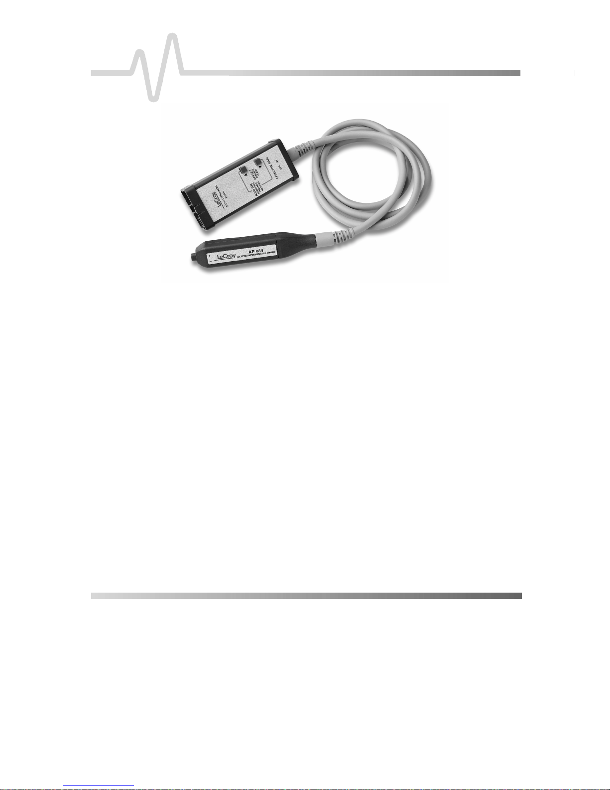
DESCRIPTION
2YHUYLHZ
The AP034 is a wide-band, active differential pr obe. The probe
features low noise, low input capacitance, high common mode
rejection, and Field Effect Tr ansistor (FET ) buffer ed inputs in the
probe head. The user-selectable offset gives the probe the
flexibility to measure a large range of signal types. Plug-on
attenuators and AC coupling accessories further extend the
application range. Included interconnect accessories allow
connection to surface mount and through-hole com ponents with
minimal signal degradation. The input receptacles in the probe
head are compatible with standard 0.025 in. (0.635 m m) square
pins, which provide a convenient, low-cost method of creating
device characterization test fixtures.
The probe is powered directly from a LeCroy oscilloscope
through the ProBus interface. T he ProBus interface also allows
local control of the probe through the os cilloscope user interface
and remote control through the inter face buses, (G PIB, RS-232).
The optional ADPPS power supply allows the AP034 to be used
with other instruments such as spectrum analyzers, network
analyzers, and oscilloscopes without ProBus interface.
APPLICATIONS
The AP034 Active Differential Probe is ideal for acquiring highspeed differential signals su ch as those found in disk drive read
channels, differential LAN, video, etc. The probe can be used
with spectrum analyzers to acquire signals in some RF systems
(for example, balanced IF mixers in hand-held cellular
telephones). The high impedance characteristics of both inputs
allow you to use the probe as an FET probe to make singleended measurements in digital systems without introducing a
ground loop, as a conventional FET probe would.
AP034-OM-E Rev D ISSUED: January 2000 ²
Page 8

CONVENTIONS USED IN THIS MANUAL
The following conventions may appear in this manual:
$3$FWLYH3UREH
Note
A Note contains general information relating to
the use of the product.
Caution
A Caution contains information that should to be
followed to avoid possible damage to the
instrument or the device under test.
WARNING
A Warning alerts you to potential injury to
yourself. Failing to adhere to the statement in a
WARNING message could result in bodily injury.
The following symbol may appear on the product:
This symbol refers you to additional information contained in this
manual. The corres ponding inform ation in the m anual is denoted
with the same symbol.
CAT I Overvoltage Installation Category per EN 61010-1
# # #
² ISSUED: January 2000 AP034-OM-E Rev D
!
Page 9

6DIHW\,QIRUPDWLRQ
OPERATOR SAFETY
The AP034 Active Differential Probe is intended to be used only
with instruments that are connected to earth ground thr ough the
input BNC connector. When you are using the probe with an
ADPPS Power Supply Adapter, make sure the adapter is
connected to a BNC connector that is grounded by the test
instrument before connecting the probe inputs to the test circuit.
Do not use the probe in wet or explosive atmos pheres. Remove
any contamination from the probe housing before connec ting the
probe inputs to any circuit. Make sure that the surface of the
probe head is completely dry before connecting the inputs.
Use of the probe, and/or the instrument it is connected to, in a
manner other than that specified may impair the protection
mechanisms.
Do not use the probe if any part is damaged. All maintenance
should be referred to qualified service personnel.
6DIHW\,QIRUPDWLRQ
# # #
AP034-OM-E Rev D ISSUED: January 2000 ²
Page 10

BLANK PAGE
$3$FWLYH3UREH
² ISSUED: January 2000 AP034-OM-E Rev D
Page 11

2SHUDWLRQ
The input circuits in the AP034 Activ e Differ ential
Probe incorporate components that protect the
probe from damage resulting from electrostatic
discharge (ESD). Keep in mind that this is an
active probe, and it should be handled carefully
to avoid damage. When using the AP034 Active
Differential Probe, you are advised to take
precautions against potential instrument damage
due to ESD.
CONNECTING THE PROBE TO THE TEST INSTRUMENT
When you are using the AP034 Active Dif ferential Probe with a
LeCroy Oscilloscope equipped with ProBus, attach the probe
output connector to the oscilloscope input connector. The
oscilloscope will recognize the probe, set the oscilloscope input
termination to 50 DQG DFWLYDWH WKH SUREH FRQWURO IXQFWLRQV LQ
the user interface.
2SHUDWLRQ
Caution
To use the AP034 Active Differ ential Probe with instrumentation
not equipped with a ProBus interface, it is necessar y to use the
ADPPS Power Supply. Attach the ADPPS connector to the probe
output connector. The output connector of the ADPPS is a
standard male BNC that can be directly connected to another
instrument. If necessary, the output of the ADPPS can be
interconnected with a 50 FRD[LDOFDEOH7RPLQLPL]HWKHHIIHFWV
of skin loss, this cable should be 1 m or less in length. The
AP034 Active Differential Probe is des igned to drive a 50 ORDG
The gain will be uncalibrated if the output is not correctly
terminated. If you are using the probe with an instrument with a
high input impedance, place a 50 %1&LQOLQHWHUPLQDWRURQWKH
instrument input before attaching the ADPPS.
CONNECTING THE PROBE TO THE TEST CIRCUIT
At the probe tip, two inputs and a ground connection are
available for connecting the probe to a circuit under test. For
accurate measurem ents, both the + and – inputs m ust always be
AP034-OM-E Rev D ISSUED: January 2000 ²
Page 12

$3$FWLYH3UREH
connected to the test circuit. The ground connection is optional.
Positive voltages applied to the + input relative to the – input will
deflect the oscilloscope trace toward the top of the screen.
To maintain the high performance capability of the probe in
measurement applic ations, user care in connecting the probe to
the test circuit. Increasing the parasitic capacitance or inductance
in the input paths may introduce a “ring,” or slow the rise time of
fast signals. To m inimize these effects, use the shortest length
possible when connecting the probe to the circuit under test.
Input leads that form a large loop area (even shielded coaxial
cables) will pick up any radiated magnetic field that passes
through the loop, and may induce noise in the probe inputs.
Because this signal will appear as a diffe rential mode signal, the
probe’s common mode rejection will not remove it. You can
greatly reduce this effect by using short interconnection leads,
and twisting them together to minimize the loop area.
High common mode rejection requires precise matching of the
relative gain or attenuation in the + and – input signal paths.
Mismatches in additional parasitic capacitance, inductance,
delay, and a source impedance differ ence between the + and –
signal paths will lower the common mode rejection ratio.
Therefore, it is desirable to us e the sam e length and type of wire
and connectors for both input connections . W hen possible, try to
connect the inputs to points in the circuit with approxim ately the
same source impedance.
If AC coupling is desired, install the AC coupling accessory on
the probe tip before connecting it to the test circuit. The low-
frequency cutoff (–3 dB point) of the AC coupler is approxim ately
16 Hz.
If the voltage in the test circuit exceeds the probe’s capability,
add the external ÷10 or ÷20 attenuator* to the probe tip. If both
the external attenuator and AC coupler are used, install the
attenuator on the probe tip first, then install the AC coupler on the
attenuator input.
* Note
The external attenuators are precisely adjusted
during manufacturing to match the
² ISSUED: January 2000 AP034-OM-E Rev D
Page 13

2SHUDWLRQ
characteristics of the input of the probe with
which they were shipped. The input
characteristics of the external attenuator itself do
not exactly match those of the probe. Therefore,
using the ÷10 and ÷20 attenuators at the same
time is not recommended. The scale factor
encoding system will not operate correctly with
both attenuators installed simultaneously.
The input characteristics of the AP034 1 GHz
Active Differential Probe are significantly
different than those of the AP033 500 MHz
Active Differential Probe. The external
attenuators are not interchangeable. The
external attenuators currently supplied with the
probes are labeled with the appropriate model
number. The attenuators supplied with model
AP033 probes prior to the introduction of the
AP034 did not include the model number on the
label. When using an external attenuator with the
AP034 Active Differential Probe, make sure it is
labeled “AP034.”
Interchanging non-compatible attenuators will
not damage the probes; however, the transient
response of the measured signals will be
significantly in error.
In addition to being compatible with the included lead set, the
probe input connectors will mate with standard 0.025 in.
(0.635 mm) square pins in any rotational orientation. To avoid
damaging the input connectors, do not attempt to insert
connectors or wire larger than 0.036 in. (0.91 m m) in diameter.
Avoid rotating square pins after they are inserted into the input
connectors.
The included accessories simplify the task of connecting the
probe to the test circuit:
• Use the small (0.5 mm) mini clips with the flexible
lead set when connecting to fine-pitch surface mount
IC leads.
AP034-OM-E Rev D ISSUED: January 2000 ²
Page 14
PROBE INPUT LOADING
$3$FWLYH3UREH
• The larger (0.8 mm) mini clips can be used to
connect to through-hole leaded components.
• The offset round pins can be used for hand-held
probing applications. Reposition the pins by rotating
them to obtain the required spacing.
Attaching any probe to a test circuit will add some loading. In
most applications, the high impedance of the AP034 Active
Differential Probe inputs im parts an insignificant load to the test
circuit. However at very high frequencies, the capacitive
reactance of the probe’s input capacitance may load the circuit
enough to affect meas urement accuracy. The equivalent model
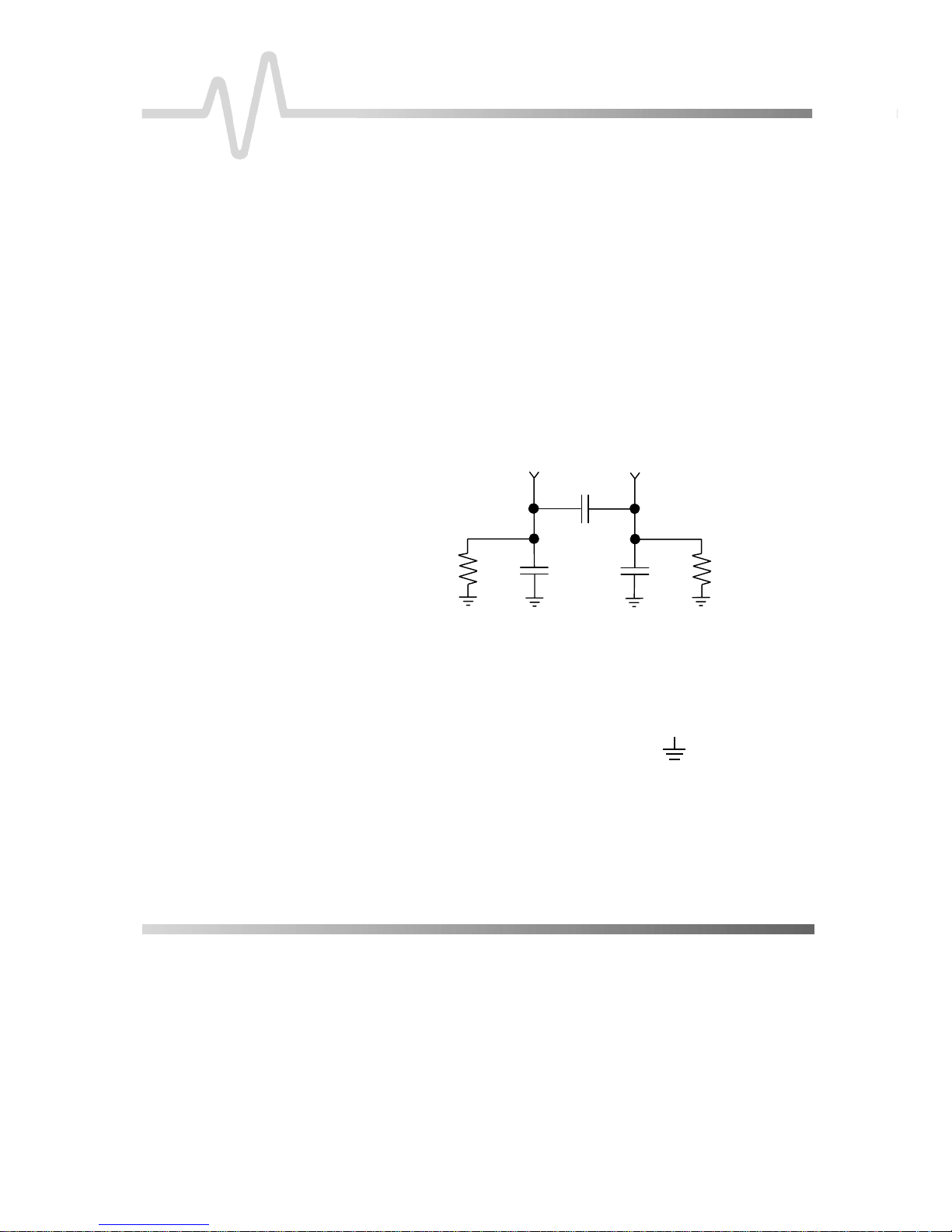
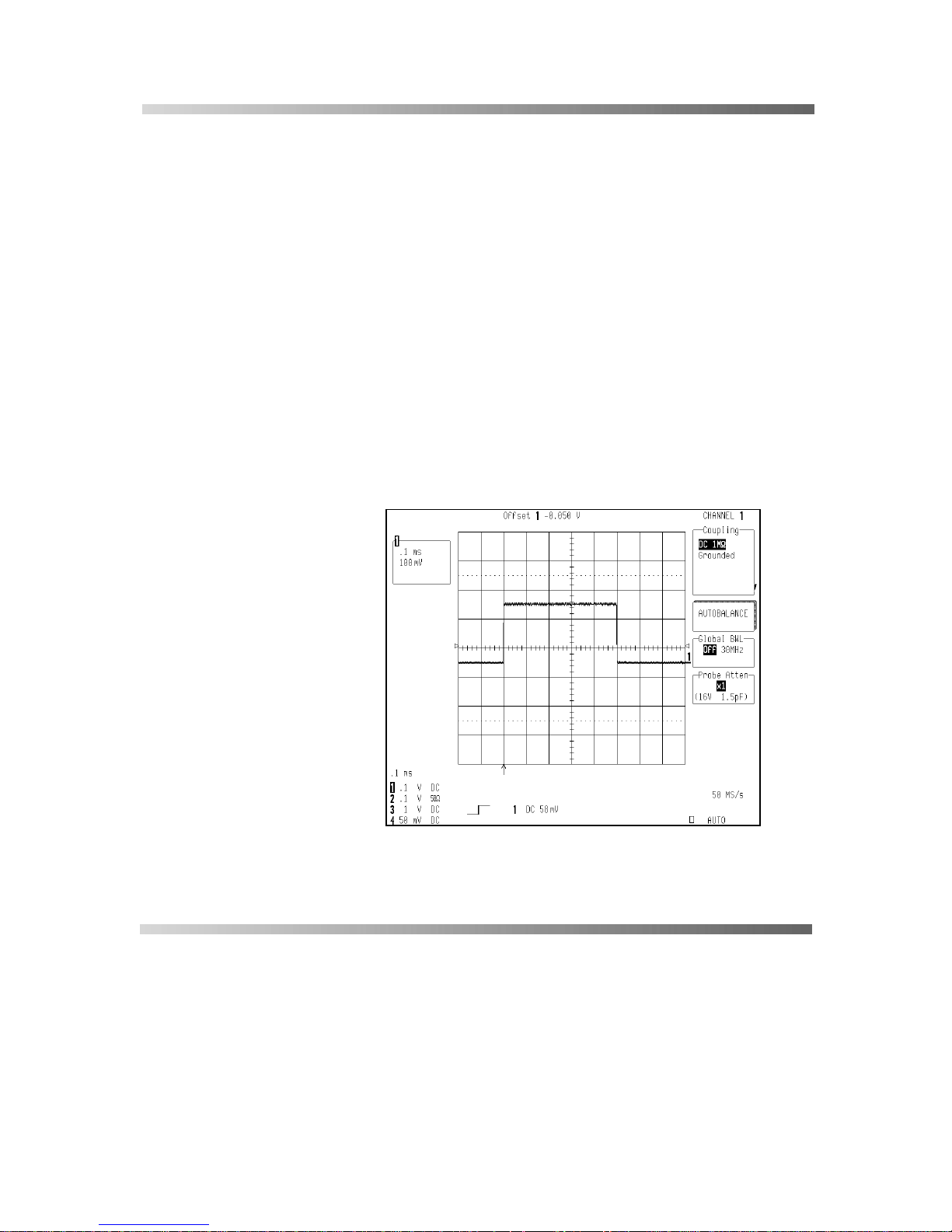
of the probe input circuits is shown below:
GROUNDING THE PROBE
+
≈ 0.1 pF
1.5 pF
1 MΩ
Figure 1. AP034 Equivalent Input Model
The single lead along with one of the larger (0.8 mm) m ini clips
can be used to ground the probe to the test circuit. Insert the pin
end of the lead into the receptacle marked:
Note
Do not use the attenuator encoding receptacle
(unmarked socket near the – input) to ground the
probe. Connecting to the encoding receptacle
will not provide adequate grounding, and may
result in in correct scale factor indication.
-
1.5 pF
1 MΩ
² ISSUED: January 2000 AP034-OM-E Rev D
Page 15

2SHUDWLRQ
In most cases it is not necessary to ground the probe to the
circuit under test. However, if the test circuit is isolated from earth
ground, it is usually necessary to connect the probe ground to a
point in the circuit. Grounding test circuits that are referenc ed to
earth ground may improve the fidelity of high-frequency
components in the waveforms. The potential for improvement
with grounding will vary depending on the common mode source
impedance. However, connecting the probe ground to a circuit
that is referenced to earth ground c an create a ground loop that
may add noise to low-amplitude signals*. Rejection of highfrequency common mode signals is improved when the probe
head is ungrounded.
The best recomm endation for connecting or not connecting the
probe ground is to try both configurations and select the one that
performs the best.
Note
The AP034 Active Differential Probe transmits
the measured signal differentially through the
probe cable. This essentially eliminates signal
degradation from ground loop effects within the
probe. However, creating a ground loop may
introduce signal distortions in the test circuit
itself, or in any coaxial cable between the
ADPPS power supply and the test instrument.
AP034-OM-E Rev D ISSUED: January 2000 ²
Page 16
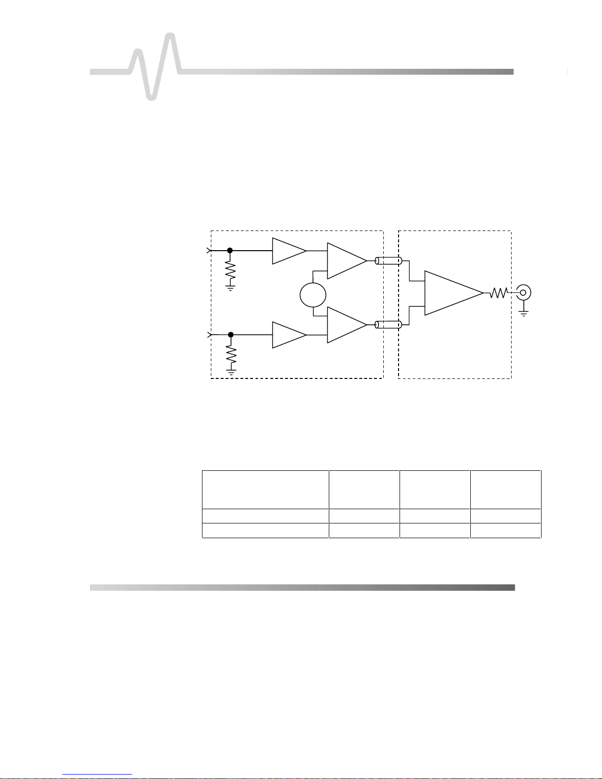
SELECTING THE PROPER RANGE
The AP034 Active Differential Probe has a fixed gain of X1
(unity). Use of the ÷10 or ÷20 external attenuators reduces the
amplitude of the input signal when it is necess ary to extend the
dynamic operating range of the probe. Attenuating the input
signal increases both the differential mode range and comm on
mode range of the probe.
Refer to the block diagram below.
$3$FWLYH3UREH
ControlProbe
+
1
-
1
By using the plug-on attenuator, you can extend the attenuation
range to ÷20. Do not use the ÷10 and ÷20 plug-on attenuators
simultaneously. The maxim um ranges are given in the f ollowing
table:
Table 1. AP034 Dynamic ranges and i nput capacitance at different attenuator
Common Mode Range
Differential Mode Range *
X1
Σ
+
V
Offs
Σ
X1
Figure 2. AP034 Block Diagram
settings
÷1
Attenuation
(Probe Only)
±16 V ±42 V ±42 V
±400 mV ±4 V ±8 V
*Offset moves the center point of this range.
Attenuation
+
-
÷10
X1
50
÷20
Attenuation
² ISSUED: January 2000 AP034-OM-E Rev D
Page 17
When us ing a differential probe or amplifier, be ca reful to avoid
exceeding the common mode range. Because the common
mode signal is rejected by the differential probe, and is not
displayed, changes in the amplitude of the common mode
component are not apparent to the user. Exceeding the c omm on
mode range may introduce distortion into the AP034 output.
Circuitry in the probe detects the presence of either attenuator,
and displays the effective gain of the probe on the probe front
panel.
OPERATION WITH LECROY OSCILLOSCOPES
When the AP034 probe is connected to a LeCroy oscilloscope
equipped with ProBus interface, the displayed scale fac tor will be
adjusted to account for the effective gain of the probe. The
channel O
FFSET knob will control the probe offset, rather than the
offset at the oscilloscope input. The probe contr ol menu can be
activated by pressing the COUPLING button while the channel to
which the probe is attached is selected.
2SHUDWLRQ
AP034-OM-E Rev D ISSUED: January 2000 ²
Figure 3. AP034 Probe Control Menu
Page 18

When the AP034 Active Differential Probe is first connected to
the oscilloscope, the following message will appear:
“WARNING: Probe offset buttons are locked.” This alerts you
that offset control m ust be m ade through the os cilloscope, rather
than through the buttons located on the probe. It does not
indicate a failure in the probe or oscilloscope.
Correct display of scale factor with the ÷20
attenuator installed and correct operation of
probe offset require that software version 8.1 or
higher be loaded. Refer to the manual section
“Oscilloscope Software Compatibility” for
additional information.
AP034 USE WITH THE ADPPS POWER SUPPLY
The optional ADPPS Power Supply allows the AP034 Active
Differential Probe to be used with instruments that are not
equipped with the ProBus interface. When used with the ADPPS,
the AP034 must be terminated into 50 ,I WKH WHVW LQVWUXPHQW
input impedance is not 50 LQVHUW D LQOLQH WHUPLQDWRU
between the ADPPS and the instrument input. If a coaxial
extension cable is used, the terminator should be located at the
instrument end of the cable. Note that the additional parasitic
losses of extension cables may reduce the usable bandwidth of
the system below the AP034 specification.
$3$FWLYH3UREH
Note:
To prevent signal distortion, it is necessary to keep the AP034
output less than 400 mV at all times.
With the ProBus interface (see note on following page), the
oscilloscope O
Without the ProBus, it is acceptable to use the oscilloscope to
position the waveform at high sensitivities , but it is a practic e that
can lead to erroneous measurements when the probe output
exceeds ±400 mV. Therefore, when the ADPPS is used, it is
preferable to use the AP034 offset function to perform all
waveform positioning.
The AP034 offset allows you to measure signals up to 2.0 V
(1.6 V of offset plus 400 mV of output signal). With accessory
plug-on attenuators, the effective offset is increased, and input
signals of 20 V (÷10) or 40 V (÷20) may be viewed. The peak
² ISSUED: January 2000 AP034-OM-E Rev D
FFSET control actually controls the AP034 offset.
Page 19
2SHUDWLRQ
signal that can be viewed at any equivalent scale factor is the
Input Differential Mode Range plus the off set used. See Adding
Offset on the following page.
When using the AP034 with the ADPPS power supply on
oscilloscopes without ProBus interface, use the following table to
select the desired effec tive volts per division and determine the
offset available.
Equivalent
Scale
Oscilloscope
Scale Factor
Factor
2 mV/Div 2 mV/Div
5 mV/Div 5 mV/Div
10 mV/Div 10 mV/Div
20 mV/Div 20 mV/Div
50 mV/Div 50 mV/Div
100 mV/Div 100 mV/Div
200 mV/Div 20 mV/Div
500 mV/Div 50 mV/Div
1 V/Div 100 mV/Div
2 V/Div 100 mV/Div
Table 2. Recommended AP034 and Os cilloscope settings to obt ain desired
AP034
Attenuation
Common
Mode Range
÷1 ±16V ±8 mV
÷1 ±16 V ±20 mV
÷1 ±16 V ±40 mV
÷1 ±16 V ±80 mV
÷1 ±16 V ±200 mV
÷1 ±16 V ±400 mV
1
÷10
÷10
÷10
÷20
1
1
1
1
2
3
±42 V ±800 mV
±42 V ±2 V
±42 V ±4 V
±42 V ±8 V
Attenuation obtained using t he external ÷10 or ÷20 attenuator.
Input differential mode range displayed is limi ted by ±4 divisions of vertic al
scale on oscilloscope.
Limited by probe output and ±4 divisions of vertical scale on oscilloscope.
Oscilloscope OFFSET and POSITI ON must be set to zero.
equivalent Volts/Divi sion
Input
Differential
Mode Range
2
2
2
2
2
3
2
2
3
3
Maximum
Offset
Maximum
Observable
Signal with
Offset
±1.6 V ±1.608 V
±1.6 V ±1.620 V
±1.6 V ±1.640 V
±1.6 V ±1.680 V
±1.6 V ±1.800 V
±1.6 V ±2.0 V
±16 V ±16.8 V
±16 V ±18 V
±16 V ±20 V
±32 V ±40 V
Input Noise
(nV/√Hz),
Typical
35
35
35
35
35
35
350
350
350
700
AP034-OM-E Rev D ISSUED: January 2000 ²
Page 20
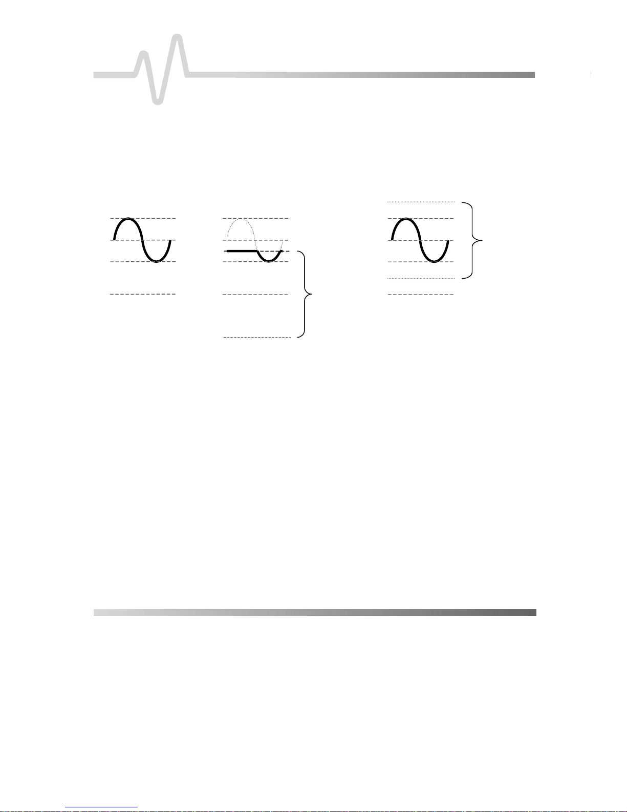
ADDING OFFSET
$3$FWLYH3UREH
The AP034 Active Differential Probe has true differential offset
capability. This allows you to remove a DC bias voltage from the
differential input signal while maintaining DC coupling. By using
probe offset rather than the P
the full dynamic range of the probe remains centered around the
offset level.
OSITION control on the oscilloscope,
+700 mV
+500 mV
+300 mV
0 mV
Input Differential
Waveform
+700 mV
+500 mV
+400 mV
+300 mV
0 mV
-400 mV
Waveform “clipped”
+700 mV
±400 mV window
re-centered around
the probe offset.
with no offset
+500 mV
+300 mV
±400 mV
centered
at 0 V
Figure 4. Effect of Dif f erential Offset
0 mV
Offset used to re-center
the differential dynami c
range around +500 mV
When the AP034 Active Differential Probe is used with a LeCroy
oscilloscope equipped with ProBus interface, the probe offset
can be controlled with the channel O
FFSET knob.* The buttons on
the probe housing will be disabled.
When used with the ADPPS Power Supply on instruments that
lack ProBus support, of fset can be c ontrolled with the buttons on
the probe’s front panel. The offset can be returned to zero at any
time by briefly pressing both the Î and Ï O
same time. Pres sing both the Î and Ï O
FFSET buttons at the
FFSET buttons for more
than 2 seconds will initiate an Autobalance cycle.
² ISSUED: January 2000 AP034-OM-E Rev D
*Note
Probe offset is controlled with the channel
O
FFSET knob in oscilloscope software versions
8.1.0 or higher. The current offset value is
Page 21

AUTOBALANCE
2SHUDWLRQ
displayed above the graticule for a few seconds
after a change is made by turning the knob (refer
to Figure 3). In prior software versions, the
channel O
oscilloscope input rather than the probe offset.
When the AP034 Active Differential Probe is
used with LeCroy oscilloscopes with older
software versions, it is important that the channel
offset (controlled by the channel O
remain set to 0.0000 V. Moving the displayed
waveform with the channel offset rather than
probe offset will not re-center the dynamic
operating range of the probe. Offsetting the trace
with the oscilloscope channel offset introduces
the possibility of erroneous waveforms that result
from overloading the probe.
The AP034 Active Differential Probe incorporates an
Autobalance function to remove the DC offset from the output.
Autobalance must be invoked by you. When power is first
applied, the probe will return to the internal values resulting from
the last Autobalance cycle. For Autobalance to function properly,
all signals must be removed from the input.
FFSET knob adjusted the offset of the
FFSET knob)
After several minutes of warmup, or when the probe is exposed
to a large shift in ambient tem perature, s ome DC off set dr ift m ay
occur from thermal ef fects in the am plifier cir cuitry. To initiate an
Autobalance cycle, remove the probe from the test circuit and
select the AUTOBALANCE menu selection in the oscilloscope
“COUPLING” menu for the channel the probe is c onnected to. If
the probe is being used with the ADPPS power supply, remove
the input signal, then push and hold both O
FFSET buttons for two
seconds. The AP034 must be terminated into 50 IRUVXFFHVVIXO
Autobalance.
Upon successful completion of the Autobalanc e c ycle, all three of
the EFFECTIVE GAIN indicators will be briefly illuminated. If an
input signal is present during auto balance and the routine fails ,
the EFFECTIVE GAIN indicators will not illuminate. The probe
will then revert to the offset values resulting from the last
AP034-OM-E Rev D ISSUED: January 2000 ²
Page 22
successful completion of the Autobalance cycle. In many
situations, this will be adequate to make routine measurements.
DESIGNING TEST FIXTURES FOR THE AP034 PROBE
Often it is desirable to connect the probe directly to userfabricated test fixtures, such as those used for semiconductor
characterization. To facilitate use with custom test fixtures, the
input receptacles used in the AP034 probe are compatible with
commercially available 0.025 in. (0.635 mm) square pins. The
receptacles do not require a specif ic rotational orientation for the
square pin. The dimensions listed below can be used as a layout
guide for a test fixture circuit board. T he recomm ended insertion
depth of the pins is 0.100 in. (2.5 mm) to 0.200 in. (5.0 mm).
Top View
Looking toward circuit board
$3$FWLYH3UREH
Side View
0.100”-
0.200”
0.110”
0.105”
0.170”
0.100”
Figure 5. Layout dimensions f or test fixtures
0.025” REF.
# # #
² ISSUED: January 2000 AP034-OM-E Rev D
Page 23

5HIHUHQFH,QIRUPDWLRQ
5HIHUHQFH,QIRUPDWLRQ
DIFFERENTIAL MODE AND COMMON MODE
Differential probes amplify the voltage difference that appears
between the + and – inputs. This voltage is referred to as the
Differential Mode or Normal Mode voltage. The voltage
component that is refer enced to earth ground, and is identic al on
both inputs, is rejected by the amplifier. This voltage is referred to
as the Common Mode voltage, because it is common to both
inputs. The common mode voltage can be expressed as:
V
VCM =
DIFFERENTIAL MODE RANGE AND COMMON MODE RANGE
The Differential Mode Range is the max imum signal that can be
applied between the + and – inputs without overloading the probe
amplifier, resulting in “clipping” or distortion of the waveform
measured by the oscilloscope.
+Input
+ V
2
-Input
The Common Mode Range is the max imum voltage with respect
to earth ground that can be applied to either input. Exceeding the
common mode range can result in unpredictable results.
Because the Common Mode s ignal is normally rejected, and is
not displayed on the oscilloscope, you need to be careful to avoid
accidentally exceeding the common mode range.
AP034-OM-E Rev D ISSUED: January 2000 ²
Page 24

$3$FWLYH3UREH
Common Mode Range
Maximum voltage from
either input to ground
Figure 6. Common Mode and Different i al Mode Range
COMMON MODE REJECTION RATIO
The ideal differential probe or diff erential amplifier would amplif y
only the differential mode voltage component and reject all of the
common m ode voltage component. Real differential probes and
amplifiers are not perfect, and a small portion of the common
mode voltage component does appear in the output. Common
Mode Rejection Ratio (CMRR) is the measure of how m uch the
probe or amplifier rejects the comm on m ode voltage com ponent.
CMRR is equal to the differential mode gain (or normal gain)
divided by the common mode gain. Com m on mode gain is equal
to the output voltage divided by the input voltage when both
inputs are driven by only the common mode signal. CMRR can
be expressed as a ratio (for exam ple, 10
(for example, 80 dB). Higher numbers indicate gr eater rejection
(better performance).
Differential Mode Range
Maximum voltage
between inputs
000:1) or implic itly in dB
The first-order term that determines the CMRR is the relative
gain matching between the + and – input paths. To obtain high
CMRR values, the input attenuators in a differential probe are
precisely matched to each other. The m atching includes the DC
attenuation as well as the capacitance that determines the AC
attenuation. As the frequency of the common m ode components
increases, the effects of stray parasitic capacitance and
inductance in determining the AC attenuation become more
pronounced. The CMRR becomes smaller as the frequency
increases. Hence, CMRR is usually specified as a plot versus
common mode frequency.
The common mode frequency in these plots is assumed to be
sinusoidal. In real life applications, the common mode signal is
² ISSUED: January 2000 AP034-OM-E Rev D
Page 25

5HIHUHQFH,QIRUPDWLRQ
seldom a pure sine wave. Signals with pulse wave shapes
contain frequency components much higher than the repetition
rate may suggest. As such, it is very difficult to predict actual
performance in the application for CMRR-versus-frequency
graphs. The practical application of these graphs is to compare
the relative common mode rejection performance between
different probes or amplifiers.
# # #
AP034-OM-E Rev D ISSUED: January 2000 ²
Page 26

BLANK PAGE
$3$FWLYH3UREH
² ISSUED: January 2000 AP034-OM-E Rev D
Page 27

&DUHDQG0DLQWHQDQFH
CLEANING
!
The exterior of the probe and cable should be cleaned only using
a soft cloth moistened with water or isopropyl alcohol. Abrasive
agents, strong detergents, or other solvents may damage the
probe. Always ensure that the input receptacles are free of debris
before connecting accessories.
CALIBRATION INTERVAL
To guarantee accurate performanc e, you should have the probe
calibrated every 12 months. Avoid exposing the probe to extreme
mechanical shock and excessive bending of the cable because
these may alter the calibration.
SERVICE STRATEGY
The AP034 circuits utilize fine pitch surface m ount devices; it is,
therefore, impractical to attempt repair in the field. Defective
probes must be returned to a LeCr oy service f a cility for diagnos is
and exchange. A defective probe under warranty will be replaced
with a factory refurbished probe. A probe that is not under
warranty can be exchanged for a factory refurbished probe. A
modest fee is charged for this s ervice. The defec tive probe mus t
be returned in order to receive credit for the probe core.
&DUHDQG0DLQWHQDQFH
TROUBLESHOOTING
If the probe is not operating properly, the problem may be the
way in which it is used. Before assuming the probe is defective,
perform the following troubleshooting procedures.
A. Trace Off Scale
This is typically caused by improper offset setting, or by an input
signal that exceeds the probe differential or common mode
range. Perform the following:
1. Remove the input signal from the pr obe, retur n the of f s et to
zero, and Autobalance the probe. Does the trace return to
approximately the center of the graticule? If not, proceed to
step 7.
AP034-OM-E Rev D ISSUED: January 2000 ²
Page 28

$3$FWLYH3UREH
2. Set the oscilloscope calibrator to output a 100-m V, 1-kHz
square wave. Using the flex lead set, connect the probe +
input to the calibrator output signal, leave the – input open.
Set the oscilloscope to 50 mV/div and 500 µs/div. Is the
displayed waveform a 100-mV, 1-kHz square wave with the
correct polarity?
3. Repeat step 2 with the – input connected to the c alibrator
and the + input left open. In this case, the displayed
waveform should be inverted.
4. Connect both the + input and – input to the calibrator
output. Is the trace approximately a flat line near zero volts?
5. If steps 1 to 4 give the correct results, the problem is likely
a result of the input signal exceeding the differential or
common mode range.
6. Connect both the + input and – input to one of the two input
signals. If the trace is off sc ale, the input signal is probably
exceeding the common m ode range. Repeat with the other
input signal.
7. Is a ProBus Power Supply Overload error message
displayed? If so, remove all other ProBus ac cessories fr om
the oscilloscope. Is the message still displayed? If so,
remove the AP034. Is the message still displayed? If so,
the oscilloscope should be returned for service.
8. If, after removing the AP034, the Power Supply Overload
error message is not displayed, the problem m ay be either
the probe or the oscilloscope. Repeat the test with a
different ProBus acces sory. If the mess age does not return
with a different accessory, the AP034 m ay be def ective and
should be returned for service.
B. Incorrect Frequency Response
Possible causes are a defective probe or oscilloscope, poor
connections, or poor grounding. Try the following:
1. Verify that the BW limiting of the oscilloscope is off.
² ISSUED: January 2000 AP034-OM-E Rev D
Page 29

C. DC Errors
&DUHDQG0DLQWHQDQFH
2. Connect the probe to another oscilloscope. If the probe
now measures properly, the problem may be in the
oscilloscope.
3. If the probe behaves as if it is ac-coupled at high frequency,
check for an open input connection.
4. Poor frequency or transient response and AC gain errors
may result when one of the two input connections is open.
5. Excessive “ring” and other transient problems can result
from exces sive lead length. To test this, shorten the input
leads to less than 1 cm. If the transient response changes
significantly, the lead parasitics are the cause.
Incorrect DC gain requires recalibration or factory repair. This
can be determined by completing the gain checks in the
Performance Verification Procedure.
1. Extremely high source resistance will result in DC gain
errors. Check the probe accuracy with the oscilloscope
calibrator signal.
2. Verify that the probe is not being overdriven into clipping for
its current gain setting.
3. Exces sive offset can result from large changes in ambient
temperature. Remove the input s ignal from the probe and
repeat the Autobalance cycle. With the Of fset set to zero,
did the trace return to the center of the graticule?
D. Poor Common Mode Rejection
Use the 1-kHz calibrator signal from the oscilloscope to check
common mode rejection. With both the + input and – input
connected to the calibrator signal, a f lat line at zero volts should
be seen on the graticule.
1. Check the probe with the plug-on attenuator installed and
removed. If excessive com mon mode signal appears only
when the attenuator is present, the attenuator m ay need to
be rematched to the probe. Use the proc edure listed in this
section to match the attenuator.
2. If the common mode signal appears when the probe is
connected to the test circuit, but not when it is attached to
AP034-OM-E Rev D ISSUED: January 2000 ²
Page 30

RETURNING A DEFECTIVE PROBE
The procedure for returning a defec tive probe to be exchanged,
is as follows:
Contact your local LeCroy sales representative to find out where
to return the product. All returned products should be identified
by model and serial number. You should describe the defect or
failure, and provide your name and contact num ber. In the case
of products returned to the factory, a Return Authorization
Number (RAN) should be used. T he RAN can be es tablished by
contacting your nearest LeCroy office, or the New York Customer
Care Center.
Return shipments should be made prepaid. LeCroy cannot
accept COD or Collect Return shipments. We recommend airfreighting. It is important that the RAN be clearly shown on the
outside of the shipping package for prompt redirection to the
appropriate LeCroy department.
$3$FWLYH3UREH
the calibrator, the problem may be caused by large
mismatches in the source impedance. T ry connecting both
inputs to one of the input signals in the test circuit, then the
other. If the comm on mode signal disappears, try probing
lower impedance points within the circuit.
1. Contact your local LeCroy sales or service representative to
obtain a Return Authorization Number.
2. Remove all accessories, including all removable cables,
from the probe.
3. Pack the probe in its case, surrounded by the original
packing material (or equivalent) and box.
4. Label the case with a tag containing:
• The RAN
• Name and address of owner
• Instrument model and serial number
• Description of the failure mode
5. Package the pr obe case in a cardboard shipping box with
adequate padding to avoid damage in transit.
² ISSUED: January 2000 AP034-OM-E Rev D
Page 31

REPLACEMENT PARTS
&DUHDQG0DLQWHQDQFH
6. Mark the outside of the box with the shipping address given
to you by the LeCroy representative; be sure to add the
following:
• ATTN: <RAN assigned by the LeCroy
representative>
• FRAGILE
7. Insure the item for the replacement cost of the probe.
8. Ship the package to the appropriate address.
The probe connection access ories, and other com mon parts c an
be ordered through the regional customer care centers. Ref er to
Figure 7 for LeCroy Part numbers. Defective probes can be
replaced on an exchange basis. The replacement exchange
probe will have been factory repaired, inspected and calibrated to
the same standards as a new product. In order to obtain an
exchange probe, you must return the defective probe. The
returned probe should be sent back to the regional customer
care center without any accessories, manual, or case.
AP034-OM-E Rev D ISSUED: January 2000 ²
Page 32

$3$FWLYH3UREH
10
3
2
1
4
5
7
6
9
8
11
12
13
14
Figure 7. Replceable Parts
² ISSUED: January 2000 AP034-OM-E Rev D
Page 33

&DUHDQG0DLQWHQDQFH
Reference LeCroy Part Number Description Rev Qty.
1 529-304-001 Plastic probe tip housing Top A 1
2 377-000-007 LeCroy AP034 Probe Tip Label A 1
3 529-304-003 Plastic probe tip housing End A 1
4 529-304-002 Plastic probe tip housing Bottom A 1
5 555-001-000 #2 Allen Screw, Black A 1
6 554-425-003 Screw, M 2.5x6, self tapping A 4
7 709-3XX-P53 ProBus End Cap A 1
8 70A-P03-303 Termination Box A 1
9 337-000-018 LeCroy Termination Box Label with
cutouts
10 416-090-004 Grey Switch Cap A 4
11 377-000-008 LeCroy Termination Box Rear
Label
12 PK033 Accessory Kit, AP033/34 without
AC Coupler and Attenuator
13 AP03X-FLEX-LEAD Flex Lead B 1
14 AP03X-OFFSET-PIN Offset Pin, package of 10 B --
A1
A1
A1
-- AP034-PROBE-FRU AP034 Probe only Exchange A --
-- AP034-DA10 Plug-On Attenuator, ÷10, AP034 A 1
-- AP034-DA20 Plug-On Attenuator, ÷20, AP034 A 1
-- AP03X-AC-COUPLER Plug-On AC Coupler,
B1
AP033/AP034
-- AP034-OM-E Instruction Manual, AP034, English D 1
AP034-OM-E Rev D ISSUED: January 2000 ²
Page 34

$3$FWLYH3UREH
MATCHING PROCEDURE FOR ÷10 PLUG-ON EXTERNAL ATTENUATOR
The ÷10 and ÷20 Plug-on attenuators provided as standard
accessories with the AP034 are calibrated to match the specific
probe they are shipped with. Individual probes will have small
variations in parasitic capacitance within the input circuits. To
obtain maximum common mode rejection performance, the
attenuators are calibrated to match a specific probe during the
manufacturing process. In order to preserve the maximum
Common Mode Rejection, do not interchange external
attenuators between probes.
The Plug-on AC coupling adapter is not matched to a specific
probe and, therefore, does not need to be matched when
interchanged.
If the ÷10 or ÷20 Plug-on attenuators becom e accidentally mixed
between probes, you can use the procedure listed below to
restore the compensation m atc h. T his adj ustment does not affect
any of the parameters in the warranted specific ations. Ther efore,
the required test equipment does not need to be calibrated.
Note
The AP033 and AP034 Active Differential Probes have
÷
different input capacitance. The
supplied with model AP033 cannot be properly adjusted
for use with model AP034. Make sure that the attenuator
is marked “AP034” before attempting this procedure.
EQUIPMENT REQUIRED
Test Oscilloscope
The oscilloscope must support ProBus. Otherwise use a nonProBus oscilloscope and ADPPS power supply.
Signal Source
Low frequency square wave: frequency from 50 Hz to 5 kHz,
amplitude from 1 V to 10 V. The output waveform m ust have a
square corner and flat top with minimum overshoot suitable for
adjusting compensation. The generator should have trigger
output, or use a BNC Tee connector and separate BNC cable
² ISSUED: January 2000 AP034-OM-E Rev D
10 Plug-on attenuator
Page 35

Interconnect Cable
Tools
PROCEDURE
&DUHDQG0DLQWHQDQFH
from the output to provide the trigger signal for the test
oscilloscope.
This is for connecting the output of the signal source to the
probe. A BNC cable and a pair of small alligator clips or “lead
grabber” adapter (Pomona #3788) may be used.
0.025 in. (0.635 mm) Squar e Pins ( 3 r equired) . T he pins f r om the
header supplied in the probe accessory kit are suitable.
Flat bladed screwdriver, 0.040 in. (1 mm) wide
Adjustment Tool: 0.025 in. (0.635 mm) square head
Note
You can fabricate the Adjustment Tool by flattening the
end of a 0.025 in. (0.635 mm) square pin with a file.
Then, using heat from a soldering iron, insert the pin into
a short length of rigid plastic tubing to serve as a handle.
1. Attach the AP034 to the test oscilloscope. If the test
oscilloscope is not equipped with ProBus, use the ADPPS to
provide power for the AP034.
2. Attach the ÷10 or ÷20 Attenuator Adapter to the AP034 probe
tip.
3. Insert 0.025 in. (0.635 mm) square pins into the +, –, and
input connectors of the Plug-on Attenuator.
4. Attach the interconnect cable to the output of the signal
source.
5. Attach the Trigger Out signal from the signal source to the
External Trigger Input of the test oscilloscope. If the signal
source does not have a separate Trigger Out signal, use a
BNC Tee connector in the output. Run one cable to the
External Trigger Input of the test oscilloscope. Connect the
other to the probe inputs.
AP034-OM-E Rev D ISSUED: January 2000 ²
Page 36

$3$FWLYH3UREH
6. Using the alligator clips on the end of the interconnect cable,
connect the signal source ground to the square pin on the
Attenuator Adapter’s “–“ input. Attach the signal output to the
square pin on the Attenuator Adapter’s “+” input.
7. Turn on the test oscilloscope. The EFFECTIVE GAIN
indicator for ÷10 or ÷20 should be lit. (NOTE: If the X1
EFFECTIVE GAIN indicator is lit instead of the ÷10 or ÷20
indicator, make sure that the plug-on adapter installed on the
probe tip is the Attenuator, and not the AC Coupler.)
8. Set the test oscilloscope Volts/Div to 200 mV (for LeCroy
oscilloscopes with ProBus) or 20 mV/Div when using the
ADPPS with an oscilloscope without scale factor correction;
5 µs/Div; AUTO trigger mode; Trigger source: External. Set
the Bandwidth Limiting to 20–30 MHz and Average the
waveform 1:31 to reduce noise.
9. Turn on the signal source. Set the output frequency to
approximately 5 kHz. Set the output amplitude to
approximately 1 V for matching the ÷10 Attenuator Adapter,
or 2 V for matching the ÷20 Attenuator Adapter.
10. Adjust the test oscilloscope trigger level for a stable trace. If
necessary, use the probe offset to position the waveform to
show the square corner of the test signal. NOTE: Do not use
the oscilloscope offset or position controls to reposition the
trace. Many of the signal generators used for compensation
calibration only have square corners on one of the two edges
of the output waveform. (Rising or falling edge, but not both.)
Be sure to display the correct edge for this step.
11. Using the square adjustment tool, adjust the +LF Comp (See
Figure 8) to achieve the best square corner and flat top of the
displayed waveform. Note that the added capacitance of the
adjustment tool may change the compensation of the
waveform when it is inserted. The correct adjustment is
achieved when the best corner is displayed with the
adjustment tool removed.
² ISSUED: January 2000 AP034-OM-E Rev D
Page 37

&DUHDQG0DLQWHQDQFH
+LF Comp.
Adjust
–LF Comp.
Adjust
DC Atten.
Balance
Figure 8. Attenuator Adjustment Locations
12. Move the connections on the interconnect cable so the signal
generator ground is connected to the square pin inserted in
the ground connector of the Attenuator Adapter. Connect the
signal generator output to BOTH the + input and – input
square pins in the Attenuator Adapter.
13. Set the signal generator frequency to about 50 Hz, and the
output amplitude to about 10 V.
14. Set the test oscilloscope Volts/Div to 20 mV (for LeCroy
oscilloscopes with ProBus) or 2 mV/Div when using the
ADPPS with an oscilloscope without scale factor correction;
and set the time scale to 2 ms/Div. It may be necessary to
increase the averaging to 1:127 to remove noise.
15. The displayed waveform is the common mode response.
Using the adjustment screwdriver with the flat blade, adjust
the DC Atten. Balance (Figure 8) to minimize the amplitude
of the flat portions of the displayed waveform. This
adjustment only affects the flat portions of the square wave.
Do not be concerned with any overshoot at the transitions.
16. Reduce the Test Oscilloscope Averaging weighting to 1:31.
Return the Volts/Div to 200 mV (for LeCroy oscilloscopes
with ProBus) or 20 mV/Div when using the ADPPS with an
oscilloscope without scale factor correction, and the Time/Div
to 5 µs.
17. Return the signal source output frequency to approximately
5 kHz. Set the output amplitude to approximately 1 V for the
÷10 Attenuator Adapter, 2 V for the ÷20 Attenuator Adapter.
18. Using the 0.025 in. square adjustment tool, adjust the –LF
Comp (Figure 8) to minimize the amplitude of overshoot
AP034-OM-E Rev D ISSUED: January 2000 ²
Page 38

$3$FWLYH3UREH
during the transition of the displayed waveform. It may not be
possible to completely eliminate the overshoot. As with the
+LF Comp adjustment, the added capacitance of the
adjustment tool may change the amplitude of the waveform
when it is inserted. The correct adjustment is achieved when
the overshoot is minimized with the adjustment tool removed.
# # #
² ISSUED: January 2000 AP034-OM-E Rev D
Page 39

3HUIRUPDQFH9HULILFDWLRQ
3HUIRUPDQFH9HULILFDWLRQ
This procedure can be used to verify the warranted
characteristics of the AP034 Active Differential Probe.
The recommended calibration interval for the model AP034
Active Differential Probe is one year. The complete perf ormance
verification procedure should be performed as the first step of
annual calibration. You can record test results on a photocopy of
the Test Record provided at the end of this section.
You can do the performance verification without removing the
instrument covers, exposing yourself to hazardous voltages.
Adjustment should only be attempted if a par am eter m easur ed in
the Performance Verification Procedure is outside of the
specified limits.
Adjustment should only be performed by qualified personnel.
TEST EQUIPMENT REQUIRED
Table 3 lists the test equipment and accessories (or their
equivalents) that are required to verify the performance of the
AP034 Active Differential Probe.
This procedure is designed to minim ize the number of calibr ated
test instruments required.
Only the parameters listed in boldface in the “Minimum
Requirements” column must be calibrated to the accuracy
indicated.
Because the input and output connector types may vary on
different brands and models of test instruments, additional
adapters or cables may be required.
AP034-OM-E Rev D ISSUED: January 2000 ²
Page 40

Description Minimum Requirements Test Equipment Examples
Wide Band Oscilloscope
TABLE 3. List of Required Equipment
1
Minimum 1 GHz bandwidth
2 mV to 5 V scale factors
ProBus interface equipped
2% vertical accuracy
$3$FWLYH3UREH
LeCroy LC584A
Digital Multimeter
DC: 0.1% accuracy
AC: 0.2% accuracy to measure
200 mV and 2 V rms @ 1 kHz
Agilent Technologies 34401A
Fluke 8842A-09
Keithley 2001
5½ digit resolution
Function Generator Sine Wave and Square Wave
output waveforms
LQWR0
20 V
p-p
70 Hz to 10 MHz frequency range
High Frequency Sine Wave
Generator
50 to 500 MHz and 50 kHz
Output adjustable from 300 mV to
2 V
p-p
Agilent Technologies 33120A
Stanford Research Model
DS340
Leader LAG-120B
Agilent Technologies 8648C
Terminator, in-line, BNC FRD[LDOWHUPLQDWLRQ Pomona 4119-50
Terminator, precision, BNC
Attenuator, BNC
BNC coaxial cable
±0.2%
÷10 (20 dB)
PDOHPDOH%1& LQ Pomona 5697-36
LeCroy TERM-CF01
Pomona 4108-20dB
(2 required)
Calibration Fixture ProBus Extension Cable LeCroy PROBUS-CF01
Calibration Fixture AP033/AP034 Calibration Fixture LeCroy AP03x-CF01
Banana Plug adapter BNC female-to-banana plug Pomona 1269
² ISSUED: January 2000 AP034-OM-E Rev D
Notes
1
If a LeCroy ProBus equipped oscilloscope is not available, you
may use an alternate oscilloscope that meets the other
minimum specifications listed, and the model ADPPS power
supply, to perform the adjustment procedure. The input
Page 41

PRELIMINARY PROCEDURE
3HUIRUPDQFH9HULILFDWLRQ
WHUPLQDWLRQ RI WKH RVFLOORVFRSH PXVW EH VHW WR DQG WKH
offset or position must remain at center screen.
1. Connect the AP034 Active Differential Probe to the
female end of the ProBus Extension Cable.
Connect the male end of the ProBus extension
cable to Channel 1 of the oscilloscope.
2. Turn the oscilloscope on and allow at least a 30minute warm-up time for the AP034 and test
equipment before performing the Verification
Procedure.
3. Tur n on the other test equipment and allow these
to warm up for the time per iod recommended by
the manufacturer.
4. While the instruments are reaching operating
temperature, make a photocopy of the
Performance Verification Test Record (located at
the end of this section), and fill in the necessary
information.
The warranted characteristics of the AP034 Active Differential
Probe are valid at any temperature within the Environmental
Characteristics listed in the Specif ications . However, som e of the
other test equipment used to verify the performance may have
environmental limitations required to m eet the accuracy needed
for the procedure. Make sure that the ambient conditions m eet
the requirements of all the test instruments used in this
procedure.
PROCEDURE
Note
Correct operation of the AP034 controls requires
oscilloscope software version 8.1.0 or higher.
The use of earlier versions is not recommended.
You can verify the software version in the test
oscilloscope by pressing the SHOW STATUS
button, then selecting the System menu option.
Contact your local LeCroy representative if the
software in your oscilloscope requires updating.
AP034-OM-E Rev D ISSUED: January 2000 ²
Page 42

A. Check Gain Accuracy
$3$FWLYH3UREH
1. From the oscilloscope display, select the channel that the
AP034 is connected to (channel 1), then select the
“Coupling” menu. Set the Coupling to DC 1 M Ω. (If the only
choice available is AC 1 MΩ, remove the Plug-on AC
Coupling adapter from the probe tip.)
2. If necess ary, set the probe offset to 0.000 V by rotating the
O
FFSET knob in the CHANNEL section of the oscilloscope.
3. Using a BNC f emale-to-female adapter, connec t one end of
a BNC cable to the probe end of the ProBus Extension
&DEOH &RQQHFW WKH 3UHFLVLRQ
end of the BNC cable.
4. Connect one end of a second BNC cable to the output of the
Function Generator. Attach the BNC-to-dual-male banana
plug adapter to the free end of the second BNC cable.
Connect the banana plugs to the Digital Multimeter (DMM).
5. Set the DMM to measure AC Volts.
6. Set the mode of the Function Generator to Sine W ave; the
frequency to approximately 1 kHz; and the output amplitude
to approximately 200 mV rms, as measured by the DMM.
7HUPLQDWRU WR WKH RWKHU
7. Record the m easured amplitude to 100 µV resolution in the
Test Record.
8. Unplug the output cable from the DMM. Remove the BNC- tobanana plug adapter from the end of the cable.
9. Autobalance the AP034 by pressing the AUTOBALANCE
menu button located in the “Coupling” menu.
10. Carefully align the four pins that correspond to the
Differential Drive No Termination portion of the AP03xCF01 Calibration Fixture with the input receptacles in the
AP034 probe head. Press the probe into the fixture to fully
engage the pins.
11. Connect the banana plugs of the precision ter minator to the
digital multimeter (DMM).
² ISSUED: January 2000 AP034-OM-E Rev D
Page 43

3HUIRUPDQFH9HULILFDWLRQ
12. Connect the free end of the output cable f rom the Function
Generator to the Differential Drive No Termination
connector of the AP033/AP034 Calibration Fixture.
13. After the DMM reading has stabilized, record the m easured
output amplitude to 100 µV resolution in the Test Record.
14. Divide the meas ured output voltage (recorded in step A-13)
by the sine wave generator output voltage (probe input
voltage) from step A-7. Subtract 1.0 from the ratio and
multiply the result by 100 to get the error in percent.
Error
15. Record the answer to two significant places (±x.xx%) on line
A-15 in the Test Record.
16. Verify that the X1 gain error is less than ±2%.
17. Disconnect both BNC cables from the test setup.
B. Check High Frequency Common Mode Rejection Ratio (CMRR)
1. Disconnect the ProBus Extension cable from the AP034 and
the oscilloscope. Reconnect the AP034 directly to the
Channel 1 input of the oscilloscope.
Common Mode Rejection Ratio (CMRR) is
defined as the Differential Mode Gain
divided by the Common Mode Gain
(normalized inverse of the Common Mode
response). At frequencies below
approximately 250 MHz, the bandwidthrelated attenuation in the AP034 Active
Differential Probe is so insignificant that
the Differential Mode Gain can be
assumed to be unity (1.0).
VoltageInput
Note
ageutput VoltMeasured O
−=
1001% ×
AP034-OM-E Rev D ISSUED: January 2000 ²
2. Care fully move the AP034 probe head from the Differential
Drive No Termination connector of the AP033/AP034
Calibration Fixture to the Common Mode Drive 50 ohm
Page 44

$3$FWLYH3UREH
Termination connector. Make sure that the probe is fully
engaged in the fixture.
3. Set the oscilloscope to display channel 1. In the oscilloscope
Channel 1 “COUPLING” menu, set Coupling to DC 1 MΩ,
and Global BWL to Off. Autobalance the AP034 by pressing
the AUTOBALANCE menu button twice. Set the
oscilloscope trigger mode to AUTO.
4. If necessary, center the trace with the Probe Off set (channel
FFSET knob).
O
5. Connec t a BNC cable from the output of the high frequency
sine wave generator to the Channel 2 input of the
oscilloscope.
6. Set the oscilloscope as follows:
Display Channel 2 only
Channel 2 VOLTS/DIV 0.5 V/div
Channel 2 Coupling DC 50Ω
Trigger on 2
Trigger coupling 2 HF
TIME/DIV 5 ns/div
Acquisition Mode NORMAL
7. Set the high-frequency sine wave generator frequency to
100 MHz, and the amplitude to approximately 2 V
. Set the
p-p
RF Output to ON.
8. Adjust the oscilloscope trigger level as needed for a stable
display.
9. Adj ust the output amplitude of the high frequency sine wave
generator for a display of exactly 4 divisions (2 V) peak-topeak. Turn off the RF Output.
10. Move the high frequency sine wave generator output cable
from the oscillos cope channel 2 input to the Common M ode
Drive 50 ohm Termination c onnector of the AP033/AP034
Calibration Fixture.
11. Set the high-frequency sine wave generator RF Output to
ON.
² ISSUED: January 2000 AP034-OM-E Rev D
Page 45

3HUIRUPDQFH9HULILFDWLRQ
12. Set the oscilloscope to display channel 1 only, set the trigger
source to channel 1, and set the channel 1 vertical scale
factor as needed to measure the amplitude of the displayed
waveform. Adjust the trigger level as neces sary for a stable
display. This is the common mode signal. Turn on Math
Channel A. Press MATH SETUP, then REDEFINE A. Set the
A Math type to Average, Avg Type to Continuous, with
1:15 weighting, of channel 1. Turn off the trace 1 display.
Note
The amplitude of the Common Mode
signal should be relatively small. If the
output waveform appears to be a 1 Volt
square wave, check that the Common
Mode Drive 50 ohm Termination
connector of the AP033/AP034 Calibration
Fixture is being used and not the
Differential Drive 50 ohm Termination
connector.
13. Measure the peak-to-peak output amplitude of the AP034.
Record the reading to two-digit resolution (xx mV) as
“Common Mode Signal at 100 MHz” in the Test Record.
14. Calculate the Common Mode Rejection Ratio (CMRR) at
100 MHz by dividing 2,000 mV by the measured Common
Mode Signal recorded in step B-14 (direct reciprocal of the
Common Mode Gain). Record the result to two-digit
resolution (xx:1) in the Test Record.
15. Verify that the CMRR at 100 MHz is greater than 18:1
(25 dB).
16. Turn off the high frequency sine wave generator RF output,
and disconnect the output cables.
AP034-OM-E Rev D ISSUED: January 2000 ²
Page 46

C. Check Low Frequency CMRR
$3$FWLYH3UREH
Note
Because greater amplitudes are required
to measure the higher CMRR
specifications at low frequencies, the
Function Generator will be used in place of
the high-frequency sine wave generator
for the low frequency CMRR test.
1. Carefully move the AP034 probe head from the Common
Mode Drive 50 ohm Termination connector of the
AP033/AP034 Calibration Fixture to the Common Mode
Drive No Termination connector. Mak e that sure the probe
is fully engaged in the fixture.
2. Set the oscilloscope to display channel 2, the channel 2 input
coupling to DC1 MΩ, the channel 2 vertical scale to
5 Volt/div, the horizontal scale to 5 ms/div, and the trigger
source to channel 2. Set BW limiting on channels 1 and 2 to
25 MHz.
3. Connect the BNC Tee adapter to the output connector of the
Function Generator. Connect a BNC cable f rom one end of
the BNC Tee adapter to channel 2 of the oscilloscope.
Connect a second BNC cable from the remaining end of the
BNC Tee adapter to the Common Mode Drive No
Termination input connector of the AP033/AP034
Calibration Fixture.
Caution
Make sure that the Common Mode Drive
No Termination connection is used.
Prolonged application of the power levels
used in the low frequency common mode
test may damage the termination
resistance in either 50 ohm Termination
input of the AP033/AP034 calibration
fixture.
² ISSUED: January 2000 AP034-OM-E Rev D
Page 47

3HUIRUPDQFH9HULILFDWLRQ
4. Set the sine wave generator frequency to 70 Hz, and the
output amplitude to 20 V
If necessary, adjust the trigger level for a stable display.
5. Set the oscilloscope to display channel 1, but leave the
trigger source set to channel 2. Set the vertical scale of
channel 1 to 2 mV/div. Create a math waveform on channel
A defined as the Average of channel 1. Set the average
factor as necessary to reduce noise. Incr ease the zoom to a
factor of four (0.5 mV/division). Turn off the waveform display
of all channels except the A Math waveform.
6. Increase the zoom of the A Math waveform as needed to
measure the peak-to-peak amplitude. This is the common
mode signal.
7. Record the displayed “Common Mode Signal at 70 Hz” to
two-digit resolution (x.xx mV) in the Test Record.
8. Calculate the Common Mode Rejection Ratio (CMRR) at
70 Hz by dividing 20
Mode Signal recorded in step C-7 (direct reciprocal of the
Common Mode Gain). Record the result to two-digit
resolution (xx
000:1) in the Test Record.
, (4 divisions on the oscilloscope).
p-p
000 mV by the measured Common
9. Verify that the “Comm on Mode Rejection Ratio at 70 Hz” is
greater than 10
000:1 (80 dB).
10. Change the output amplitude of the Function Generator to
approximately 8.0 V
, and the frequency to 1 MHz.
p-p
11. Set the oscilloscope to display channel 2 only. Change the
horizontal scale factor to 0.5 µs/div, and the channel 2
vertical scale to 2 V/div. Turn the BW L on channels 1 and 2
to 200 MHz.
12. Adjust oscilloscope trigger level as necessary for a stable
display. Adjust the Function Generator amplitude as needed
to maintain 8.0 V
as measured on channel 2.
p-p
13. Turn off the oscilloscope channel 2 display, turn on the
display of channel 1 and the A Math waveform (averaged
channel 1). Adjust the scale factor of channel 1 and the
Zoom of the A M ath waveform as necessary to accurately
measure the amplitude of the averaged signal.
AP034-OM-E Rev D ISSUED: January 2000 ²
Page 48

$3$FWLYH3UREH
14. Record the displayed “Common Mode Signal at 1 MHz” to
two-digit resolution in the Test Record.
15. Calculate the “Common Mode Rejection Ratio (CMRR) at
1 MHz” by dividing 8000 mV by the measured Common
Mode Signal recorded in step C-14. Record the result in the
Test Record.
16. Verify that the Common Mode Rejection Ratio at 1 MHz is
greater than 100:1 (40 dB).
17. Remove all cables and test fixtures from the AP034 probe.
This completes the Performance Verification of the AP034.
Complete and file the results recorded in the AP034 Performance
Verification Test Record, as required by your quality procedures.
Apply a suitable calibration label to the AP034 housing as
required.
# # #
² ISSUED: January 2000 AP034-OM-E Rev D
Page 49

3HUIRUPDQFH9HULILFDWLRQ
AP034 Performance Verification Test Record
This record can be used to record the results of measurements made during the performance
verification of the AP034 Active Differential Probe.
Photocopy this page and record the results on the copy. File the completed rec ord as required by
applicable internal quality procedures.
The section in the test record corresponds to the parameters tested in the performance
verification procedure. The numbers preceding the individual data records correspond to the steps
in the procedure that require the recording of data. Results to be recorded in the column labeled
“Test Result” are the actual specification limit check . The test limits are included in all of these
steps. Other measurements and the results of intermediate calculations that support the limit
check are to be recorded in the column labeled “Intermediate Results.”
Permission is granted to reproduce these pages for the purpose of recording test results.
Model: __________AP034_________
Serial Number: _________________________
Asset or Tracking Number: _________________________
Date: _________________________
Technician: _________________________
EQUIPMENT USED:
MODEL SERIAL
NUMBER
OSCILLOSCOPE
DIGITAL MULTIMETER
HF SINE WAVE GENERATOR
FUNCTION GENERATOR
1
The function generator provides st i mulus for making rel ative measurements . The output amplitude of t he generator is
measured with the DMM or oscilloscope in the procedure. Thus, the generator is not required to be calibrat ed.
AP034-OM-E Rev D ISSUED: January 2000 ²
1
CALIBRATION
DUE DATE
N/A
Page 50

$3$FWLYH3UREH
AP034 PERFORMANCE VERIFICATION TEST RECORD
Step Description Intermediate Data Test Result
Gain Accuracy
A-7 Sine Wave Generator Output Voltage ________________ mV
A-13 Probe Output Voltage ________________ mV
A-15 Gain Error (Test Limit 2%) _________________%
High Frequency Common Mode Rejection Ratio (CMRR)
B-13 Common Mode Signal at 100 MHz ________________ mV
B-15 CMRR at 100 MHz (Test Limit _________________:1
Low Frequency Common Mode Rejection Ratio
C-7 Common Mode Signal at 70 Hz ________________ mV
C-8 CMRR at 70 Hz (Test Limit
C-14 Common Mode Signal at 1 MHz ________________ mV
C-15 CMRR at 1 MHz (Test Limit _________________:1
Notes: _______________________________________________________________________
_____________________________________________________________________________
_____________________________________________________________________________
_____________________________________________________________________________
_____________________________________________________________________________
_____________________________________________________________________________
_____________________________________________________________________________
_____________________________________________________________________________
_____________________________________________________________________________
_____________________________________________________________________________
_____________________________________________________________________________
_____________________________________________________________________________
000:1) _________________:1
² ISSUED: January 2000 AP034-OM-E Rev D
Page 51

$GMXVWPHQW3URFHGXUH
INTRODUCTION
You can use this procedure to adjust the AP034 Active
Differential Probe to meet the warranted specifications. This
procedure should only be performed if the instrument fails the
Performance Verification tests.
If the probe cannot be adjusted to meet the Performance
Verification limits, repair may be necessary.
To ensure instrument accuracy, check the calibration of the
AP034 Active Differential Probe every year. Before calibration,
thoroughly clean and inspect this unit as discussed in the
“Cleaning” section.
Completion of each step in the Adjustment Procedure ensures
that the differential probe meets specifications. Some of the
adjustments interact with other parts of the circ uitry. Therefore, it
is necessary that all adjustments be performed in the order listed.
For best overall instrument perform ance, make eac h adjustment
to the exact setting, even when adjustment is within the limits
stated in the procedure.
$GMXVWPHQW3URFHGXUH
Adequate guard bands were designed into the AP034 Active
Differential Probe to ensure that it will meet or exceed published
specifications over the entire operating temperature range. To
continue to meet the environmental specifications, all
adjustments mus t be performed in a c ontrolled environment with
an ambient temperature of 25 ±5 Û& 7KH $3 $FWLYH
Differential Probe mus t also be at stable operating temperature
before performing adjustments.
Caution
The adjustment procedure will require removal of
the probe covers. These covers are part of the
ESD protection system of the AP034 Active
Differential Probe. To protect the probe, you
should perform the entire procedure on a static
dissipating work surface. Wear an antistatic
AP034-OM-E Rev D ISSUED: January 2000 ²
Page 52

TEST EQUIPMENT REQUIRED
$3$FWLYH3UREH
grounding wrist strap and follow standard static
control procedures.
The probe tip housing provides physical rigidity
to the input pins of the probe. When the covers
are removed, observe extra caution to avoid
breaking the probe tip receptacles when mating
the probe to the calibration fixture.
The table on the next page lists the test equipment and
accessories, or their equivalents, that are r equired for complete
calibration. Specifications given for the test equipment are the
minimum nec es sa ry for acc ur ate c alibra tion. All test equipment is
assumed to be correctly calibrated and operating within the
specifications listed. Detailed operating instructions for the test
equipment are not given in this procedure. Refer to the test
equipment manual if more information is needed.
If alternate test equipment is substituted, control settings or
calibration equipment setups m ay need to be altered. Alternate
models of test equipment may have different connector styles
requiring adapters not included in the equipment list.
² ISSUED: January 2000 AP034-OM-E Rev D
Page 53

$GMXVWPHQW3URFHGXUH
TABLE 4. Test Equipment and Accessories
Description Minimum Specifications Test Equipment Examples
Wide Band Oscilloscope*500 MHz bandwidth
2 mV to 200 mV vertical scale
LeCroy LT342
LeCroy LC344A
factors
ProBus interface equipped*
2% vertical accuracy
Digital Multimeter 0.1% DC volts accuracy at 0.4 V
0.2% AC volts accuracy at 2 V
and 1 kHz
Agilent Technologies 34401A
Fluke 8842A-09
Keithley 2001 with test leads
5½ digit resolution
0.01 mV AC volts resolution
Function Generator Sine and square wave output
LQWR0
20 V
p-p
50 Hz to 1 MHz frequency range
Sync. or Freq. Reference output
Fast Rise Pulse
Generator
Risetime < 2 ns
$PSOLWXGH!P9LQWR
Over/Undershoot < 6%
Agilent Technologies 33120A
Stanford Research Model
DS340
Leader LAG-120B
Calibrator signal from LeCroy
oscilloscope
Tegam / Tektronix PG506 with
power unit
Sine Wave Generator Output 250 MHz at 1 V rms Agilent Technologies 8648C,
with male N to female BNC
adapter for the output connector
Tegam SG504 with TM series
mainframe.
DC Voltage Source 0 to 2 VDC regulated output,
HP 6633A
settable to 1 mV resolution
Termination, precision LeCroy TERM-CF01
Termination, BNC WKURXJKPDOHIHPDOH Pomona 4119-50
Calibration Fixture ProBus Extension Cable LeCroy PROBUS-CF01
Calibration Fixture AP033/AP034 Calibration
LeCroy AP03X-CF01
Fixture
AP034-OM-E Rev D ISSUED: January 2000 ²
Page 54

$3$FWLYH3UREH
TABLE 4. Test Equipment and Accessories
Description Minimum Specifications Test Equipment Examples
BNC coaxial cable
(2 required)
BNC Tee Adapter female-male-female Pomona 3285
Banana Plug Adapter
(2 required)
Shorting Plug Two 0.025 in. square pins on
Adjustment Tool 0.025 in. square tip Johanson 4192
Low Capacitance
Screwdriver
If a LeCroy ProBus equipped oscilloscope is not available, you may perform the adjustment
procedure with an alternate oscilloscope that meets the other Minimum Specifications, and the
PRGHO$'336SRZHUVXSSO\ 7KH LQSXWWHUPLQDWLRQRI WKH RVFLOORVFRSHPXVWEH VHWWR
offset or position must remain at center screen, and the high-frequency adjustments must be
performed with the ADPPS connected directly to the input of the oscilloscope.
PRELIMINARY PROCEDURE
male-male BNC, approx. 1 m Pomona 5697-36
BNC female-to-dual male
banana plug
0.100 in. centers
* Notes
1. Using pliers, carefully remove each of the push buttons f rom
the ProBus interface housing by gently pulling them away
from the housing.
Pomona 1269
Supplied with AP03X-CF01
WKH
2. Remove the two screws that secure the plastic cover on the
cable end of the ProBus interface housing. Gently pull on the
probe cable to slide the circuit board assembly from the metal
housing.
3. Rem ove the 5/64 in. (2 mm) Allen head cap scr ew from the
small cover on the back of the probe tip. Rem ove the cover
along with the small cover on the opposite side of the pr obe.
Hold the shielded portion of the probe head in one hand and
² ISSUED: January 2000 AP034-OM-E Rev D
Page 55

$GMXVWPHQW3URFHGXUH
gently slide the larger cover off by pulling it away from the
probe tip end.
4. Connect the AP034 Active Differential Probe output to the
female end of the ProBus Extension Cable. Be careful to align
the ProBus pins with the corresponding connector cor rectly.
Connect the male end of the ProBus Extension Cable to
Channel 1 of the oscilloscope.
Note
The Logic board is connected to the
Amplifier board by four small 8-pin
connectors. There are no additional
mechanical fasteners holding the two boards
together. A small foam pad mounted on the
circuit board ensures that the connectors
remain engaged while the assembly is
mounted within the ProBus interface
housing. Be sure that the connectors
between the boards are firmly engaged
before applying power to the probe.
Operating the probe without the logic board
will not damage it. However, to ensure
reliable operation, the logic board should
only be mated with the Amplifier board with
the power removed, and the ProBus
connector disengaged.
5. Apply power to the oscilloscope and to the other test
instrumentation. Allow at least 30 minute’s warm-up time for
the AP034 Active Differential Probe and test equipment
before continuing the calibration procedure.
Note
The probe tip cover also serves to thermally
stabilize the input circuitry. The differential
input stage of the probe utilizes discrete
transistors that need to maintain an
approximate match of junction temperatures
for correct DC balance. With the covers
removed, this circuitry is susceptible to drift
caused by air currents flowing over the
AP034-OM-E Rev D ISSUED: January 2000 ²
Page 56

$3$FWLYH3UREH
components. Remove or redirect any fans
that may be blowing air currents over the
probe tip during adjustment.
Note
Correct operation of the AP034 Active
Differential Probe controls requires software
version 8.1.0 or higher. You can find out the
software version loaded on your LeCroy
scope by pressing SHOW STATUS, then
selecting the System menu option.
In version 8.1.0 and higher, the OFFSET
controls on the front panel of the pr obe are
disabled. Offset is controlled by the O
knob in the oscilloscope CHANNEL section.
FFSET
² ISSUED: January 2000 AP034-OM-E Rev D
Page 57

PROCEDURE
A. Adjust Coarse DC Balance (R226)
1. If necessary, set the probe offset to 0.000 V by rotating the
O
2. Insert the two-pin shorting plug into the sock et on the Logic
Board. Use the two holes closest to the probe cable
(Figure 9).
$GMXVWPHQW3URFHGXUH
FFSET knob in the CHANNEL section of the oscilloscope.
AP033 Logic Board
Installation Location for Shorting Strap
Figure 9.
3. To enter the Cal Mode, push either of the two offset buttons
that protrude through holes in the Logic Board.
4. Plug the precision 50 WHUPLQDWRULQWRWKH'00LQSXW6HW
the DMM to measure DC volts.
5. Using a low capacitance screwdriver, adjust Coarse DC
Bal (R226) on the Amplifier Board f or an output voltage of
0 mV ±10 mV (Figure 10).
AP034-OM-E Rev D ISSUED: January 2000 ²
Page 58

$3$FWLYH3UREH
B. Adjust Fine DC Balance (R304)
1. Remove the shorting plug from the Logic Board.
2. Reinsert the shorting plug into the two holes near the end
3. Reenter Cal Mode by pushing either of the two buttons that
4. 5HPRYHWKH%1&FDEOHIURPWKHSUHFLVLRQ
5. Short the output BNC connector by reconnecting the cable
6. In Cal Mode, the EFFECTIVE GAIN indicators serve as an
R226
Coarse DC Bal
Figure 10. Amplifier Board A dj ustment Locations
R322C
Gain
R330
Offset
R304
Fine DC Bal
of the Logic Board. (Figure 9.)
protrude through holes in the Logic Board.
WHUPLQDWRU
connected to the DMM.
to the SHORT connector on the AP033/AP034 Calibration
Fixture. The SHORT connector is the only BNC connector
on the AP033/AP034 Calibration Fixture that does not have
corresponding input pins for the probe tip. It is located on
the end of the board beyond the Common Mode
Terminated connector.
adjustment indicator. T he EFFECTIVE G AIN indicators are
located on the Logic Board (Figure 11). It may be
necessary to hold the boards in your hands to see the
indicators while making the adjustment.
² ISSUED: January 2000 AP034-OM-E Rev D
Page 59

$GMXVWPHQW3URFHGXUH
7. Using a low capacitance screwdriver, adjust Fine DC
Balance (R304) until the ÷10 EFFECTIVE G AIN indicator
lights (Figure 11).
8. Disconnect the BNC cable from the short connector.
Remove the shorting plug from the logic board.
C. Adjust Low Frequency CMRR (R7)
1. Leave the BNC cable connected to the probe end of the
ProBus extension cable. Connect a 50 %1& 7KURXJK
Terminator on the other end of the BNC cable. Connect the
male end of the 50 WHUPLQDWRUWRFKDQQHORQWKHVFRSH
The scope end of the ProBus extension cable should
remain connected to channel 1 of the scope, although there
is no signal cable connected.
2. Connect a BNC cable from the output of the Function
Generator to the Channel 2 input of the oscilloscope.
AP033 Logic Board
Figure 11. ÷11 Effective Gain Indicator
Effective Gain Indicators
Adjustment too far
counter-clockwise
÷10 Indicator:
Adjustment correct
Adjustment too far
clockwise
3. Connect a second BNC cable from the Function Generator
SYNC OUT to the external trigger input of the oscilloscope.
4. Set the Function Generator waveform to Sine and the
frequency to 70 Hz.
AP034-OM-E Rev D ISSUED: January 2000 ²
Page 60

$3$FWLYH3UREH
5. Set the oscilloscope as follows:
Display: Channel 2
Channel 1 VOLTS/DIV: 2 mV/div
Channel 2 VOLTS/DIV: 5 V/div
Channel 2 Coupling: '&0
Channel 3 VOLTS/DIV: 2 mV/div
Channel 3 Coupling: AC 1M
Trigger on: EXT10
cplg EXT10: DC
TIME/DIV: 10 ms/div
Acquisition Mode: NORMAL
6. Adjust the trigger level for a stable display.
7. Set the Function Generator output voltage to 20 V
p-p
as
displayed on the oscilloscope.
8. Disconnect the output cable of the function generator f rom
the channel 2 input of the oscilloscope and rec onnect it to
the Common Mode Drive No Termination connector of
the AP033/AP034 Calibration Fixture.
9. Carefully align the four pins that correspond to the
Common Mode Drive No Termination portion of the
AP033/AP034 Calibration Fixture with the input receptacles
in the AP034 probe head. Press the probe into the fixture to
fully engage the pins.
10. Set the oscilloscope to display channel 3. The waveform is
the common m ode signal. Turn the offset as neces sary to
keep the trace on screen. Turn on Math Channel A. Press
MATH SETUP, then REDEFINE A. Set the A Ma th type to
Average, Avg Type to Continuous, with 1: 15 weighting,
of channel 3. Turn off the trace 3 display. Use the Math
Zoom and Position controls as necessary to view the
waveform.
11. Adjust LF CMRR (R7) for minimum am plitude. (See Figure
12 for location.)
² ISSUED: January 2000 AP034-OM-E Rev D
Page 61

$GMXVWPHQW3URFHGXUH
D. Adjust OFFSET (R330)
R7
LF CMRR
Figure 12. Probe Tip Adjustment Locations
C18A
Attenuator CMRR
C17A
Attenuator Comp
12. Remove the BNC cable from the output of the Function
Generator and the calibration fixture. Leave the BNC cable
from the SYNC output to the oscilloscope external trigger
input in place.
1. Reconnect the BNC cable to both ends of the ProBus
extension cable. The oscilloscope end of the extension
cable should still be connected to channel 1.
2. Set the oscilloscope channel 1 scale factor to 10 mV/div,
and the acquisition mode to Auto. Set the BWL to 20 or
25 MHz. Adjust the OFFSET to 0.0 mV
3. Carefully move the AP034 probe tip from the Common
Mode Drive No Termination position of the AP033/AP034
Calibration Fixture to the Differential Drive No
Termination position. Press the probe into the fixture to
fully engage the pins.
4. Connect female BNC-to-dual male banana plug adapters to
each end of the BNC cable. Plug one end into the output of
the DC voltage source, making sure the plug corresponding
to the BNC shield (marked “Ground”) is connected to the
voltage source –Output (or common for dual supplies)
connector, and the other pin on the +Output connector.
AP034-OM-E Rev D ISSUED: January 2000 ²
Page 62

$3$FWLYH3UREH
5. Connect the other end of the cable to the DMM input,
making sure that the plug corresponding to the BNC shield
(marked “Ground”) is connected to the LO or COM input.
6. Set the DC Voltage Source to read as close as possible to
+1.600 V on the DMM.
7. Autobalance the AP034 by pressing the AUTOBALANCE
menu button located in the “COUPLING” menu twice, or by
pressing and holding both probe offset buttons for at least
two seconds.
8. Disconnect the BNC cable from the female BNC-to-dual
male banana plug adapter on the DMM.
9. Reconnect the BNC cable f rom the DC Voltage Source to
the Differential Drive No Termination connector on the
AP033/AP034 Calibration Fixture.
10. Set the probe offset to –1.600 V by rotating the OFFSET
knob in the channel section of the oscilloscope.
11. Allow 10 seconds for the AP034 to stabilize.
12. Using a low capacitance screwdriver, adjust Offset (R330)
to bring the trace back to exactly center screen. (See
Figure 10 for adjustment location.)
13. Remove the dual banana plug adapter from the output of
the DC voltage source and reconnect it, with the pins
reversed. (The plug corresponding to the BNC shield
(marked “Ground”) should now be connected to the
+Output connector.)
14. In the CHANNEL menu of the oscilloscope, set the probe
offset to +1.600 V by rotating the OFFSET knob.
15. Allow 10 seconds for the AP034 to stabilize.
16. Note the amplitude of the trace from center screen.
17. Adjust Offset Cal (R330) to position the trace to
approximately ½ the am plitude from center s creen noted in
the previous step. This am plitude should be within ±10 mV
of center screen. Note this value.
² ISSUED: January 2000 AP034-OM-E Rev D
Page 63

$GMXVWPHQW3URFHGXUH
18. Again, remove the dual banana plug adapter from the
output of the DC voltage source and reconnect it, with the
pins reversed. The plug corresponding to the BNC shield
(marked “Ground”) should now be connected to the – or
Common Output connector.
19. In the CHANNEL menu of the oscilloscope, set the probe
offset to –1.600 V by rotating the OFFSET knob.
20. Allow 10 seconds for the AP034 to stabilize.
21. T he trace should be offset f rom the c enter line by the same
amplitude but opposite polarity of the value noted in step
E-16.
22. Repeat steps E-13 through E-21 as necessary until the
errors at +1.6 V and at –1.6 V are approxim ately equal, and
both are within 10 mV of the center scale. Reverse the
polarity of the dual banana plug adapter at the output of the
DC voltage source, and the corresponding probe offset
value with each repetition.
23. Disconnect the cable from the DC Voltage Source. Keep
the AP033/AP034 Calibration Fixture connected to the
AP034 for the next step.
E. Adjust GAIN (R322C)
1. Set the AP034 offset to 0.000 V by rotating the OFFSET
knob in the CHANNEL section of the oscilloscope.
2. Disconnect the BNC cable from the oscilloscope end of the
ProBus extension cable. Reconnect this end of the cable to
the precision 50 Ω termination.
3. Connect one end of a second BNC c able to the output of
the Function Generator. Connect the BNC-to-dual male
banana plug adapter to free the end of the BNC cable.
Insert the banana plugs of the adapter into the input
terminals of the Digital Multimeter (DMM).
4. Set the DMM to measure AC volts.
5. Set the mode of the Function Generator to Sine W ave, the
frequency to approximately 1 kHz and the output am plitude
to read approximately 190 mV on the DMM.
AP034-OM-E Rev D ISSUED: January 2000 ²
Page 64

6. Record the DMM reading. Be careful not to alter the output
amplitude of the generator after the measured value has
been recorded
7. Remove the banana plug adapter and connect the free end
of the cable to the Differential Drive no Termination
connector on the calibration fixture.
8. Connect the AP034 Output cable with 50 Ω Precision
termination to the DMM.
9. Using a low capacitance screwdriver, adjust GAIN (R322C)
so that the DMM reading is within ±1 mV (0.5%) of the
reading recorded in step E-6. (See Figure 10 for
adjustment location.)
10. Disconnect the Function Generator, DMM, calibration
fixture, and precision 50 Ω terminator.
F. Adjust Final Attenuator Compensation (C17)
The calibrator signal from a LeCroy
oscilloscope is the recommended signal
source for this adjustment. If another
oscilloscope is being used for this
procedure, make sure that the square
wave source has adequate flatness
(minimum overshoot and undershoot.)
$3$FWLYH3UREH
Note
1. Press the U
menu. Set the mode to CAL signal, Shape to Square,
Amplitude to 1 V into 1 MΩ, and Frequency to 1 kHz.
2. Reconnect the free end of the ProBus Extender BNC cable
to the oscilloscope end of the extender located on
channel 1.
3. Connect a BNC cable from the CAL output BNC connector
to the Differential Drive 50 ohm Termination connector
on the AP033/AP034 Calibration Fixture.
4. Carefully connect the Differential Drive 50 ohm
Termination portion of the AP033/AP034 Calibration
² ISSUED: January 2000 AP034-OM-E Rev D
TILITIES button, then select the CAL BNC Setup
Page 65

Fixture to the probe tip. Press the probe into the fixture to
fully engage the pins.
5. Set the oscilloscope display to channel 1, vertical scale
factor to 50 mV/div and the horizontal scale to 1 µs/div.
Set the trigger source to channel 1, and Slope to Positive.
Adjust the oscilloscope trigger level as necessary for a
stable display.
6. Using the OFFSET control, m ove the trace down until the
top portion of the waveform is centered.
7. Using the 0.25 in. square adjustment tool, adjust
Attenuator Comp (C17A) for a flat top waveform. (See
Figure 12 for adjustment location.)
8. Remove the cable from the CAL output connector on the
scope.
G. Adjust Final Attenuator CMRR (C18A)
1. Carefully move the AP033 probe head from the Differential
Drive 50 ohm Termination portion of the AP033/AP034
Calibration Fixture to the Common Mode Drive 50 ohm
Termination portion.
$GMXVWPHQW3URFHGXUH
2. Remove the BNC cable from the Differential Drive 50
ohm Termination connector of the AP033/AP034
Calibration Fixture. Connect one end of the BNC cable to
the Common Mode Drive 50 ohm Termination connector
of the AP033/AP034 Calibration fixture. Connect the other
end of the cable to the female end of a BNC Tee adapter.
Plug the male connector of the BNC T ee adapter into the
channel 4 input of the oscilloscope. Connect a s econd BNC
cable to the remaining female connector of the BNC Tee
adapter. Connect the other end of the second BNC cable to
the CAL output BNC connector.
3. Set the oscilloscope display to channel 4, coupling to
'&0
, vertical scale factor to 200 mV/div, and the trigger
source to channel 4. Adjust the oscillos cope tr igger level as
necessary for a stable display.
4. Set the oscilloscope to display channel 1, and vertic al sc ale
factor to 10 mV/div. Set the OFFSET to 0.0 mV
AP034-OM-E Rev D ISSUED: January 2000 ²
Page 66

5. Adjust Attenuator CMRR (capacitor C18A) for minimum
6. Leave the setup connected for the next step.
H. Assemble Probe and Amplifier
1. Car efully slide the large probe tip cover over the probe tip,
2. Snap the small probe c over with the threaded brass insert
3. Place the lip on the large end of the remaining cover under
4. Replace the
$3$FWLYH3UREH
amplitude shift of the displayed waveform at the trigger
point in time. See Figure 10 for adjustment location.
being careful to engage the input pins.
onto the bottom of the probe. Engage the probe cable
strain relief into the mating area of the cover. Carefully
dress the wires entering the cable to clear the area above
the brass insert.
the mating surface near the probe tip. Gently press the
cover into place. If the cover appears not to close
completely, remove it and again check for adequate
clearance between the brass insert and the cable wires.
5
/64 in. Allen cap screw and tighten.
5. Hold the Logic Board/Amplifier Board assembly in one
hand with the Logic board facing up. Hold the ProBus
Interface housing in the other hand with the control side
(side with holes for the buttons) facing up.
6. Align the edges of the Amplifier Board with the slots in the
center of the inside of the housing. (T he amplifier board is
the thicker circuit board and has the BNC connector
soldered to it.) Slide the boards into the housing, being
careful to align the screw holes in the end cover with the
corresponding channels in the corners of the housing.
7. Insert and tighten the two screws that secure the end panel
to the ProBus interface housing. Avoid overtightening the
screws because the cover may warp.
8. Replace the four push button caps, pressing each fully to
seat the cap on the button shaft.
² ISSUED: January 2000 AP034-OM-E Rev D
Page 67

I. Attenuator Matching and Final Check
1. Repeat the Performance Verification procedure to ensure
compliance with the warranted specifications.
2. Perf orm the Attenuator Matching Procedure listed on page
5-8. Apply calibration seals in accordance with your quality
procedures.
This concludes the Adjustment Procedure. Repeat the
Performance Verif ic ation proc edur e to complete the calibration of
the AP034.
$GMXVWPHQW3URFHGXUH
# # #
AP034-OM-E Rev D ISSUED: January 2000 ²
Page 68

BLANK PAGE
$3$FWLYH3UREH
² ISSUED: January 2000 AP034-OM-E Rev D
Page 69

6SHFLILFDWLRQV
NOMINAL CHARACTERISTICS
6SHFLILFDWLRQV
The following specifications are valid for model AP034 probes
after the probe has reached operating temperature. This takes
20 minutes with power applied, in an environment with stable
ambient temperature. The probe must be operating within the
environmental conditions listed in the General Characteristics
section, and must have been calibrated within the past 12
months in an ambient temperature of 23 ±5
Nominal characteristics describe parameters and attributes that
are guaranteed by design, but do not have associated
tolerances.
Input Configuration: True Differential (+ and –
Inputs); with shield Ground
connector.
1
Effective Gain
:X1, ÷101, ÷20
°
C.
1
Input coupling: DC. AC Coupling obtained by
installing AC Coupling Adapter.
Differential Mode Range: ±400 mV (÷1 Attenuation)
±4 V (÷10 Attenuation
±8 V (÷100 Attenuation
Common Mode Range: ±16 V (÷1 Attenuation)
±42 V (÷10 Attenuation
±42 V (÷20 Attenuation
1
)
1
)
1
)
1
)
Maximum Input Voltage: ±42 V either input from ground
AP034-OM-E Rev D ISSUED: January 2000 ²
Page 70

WARRANTED ELECTRICAL CHARACTERISTICS
Warranted characteristics are parameters with guaranteed
performance. Unless otherwise noted, tests are provided in the
Performance Verification Procedure for all warranted
specifications.
LF Gain Accuracy: 2% into 50.0 Ω load
Common Mode Rejection Ratio
1
Notes:
÷10 and ÷20 obtained with external plug-on attenuators
2
Output impedance is 50 Ω, intended to drive 50 Ω. Add
uncertainty of termination impedance to accuracy.
3
LeCroy measures CMRR with a fixture that connects
the probe tip ground to the signal source ground. This
method is necessary to obtain a reproducible CMRR
measurement.
Often, users leave the probe tip ungrounded when
measuring high frequency signals. Not grounding the
probe tip can actually improve CMRR by allowing
some of the common mode signal to be impressed
across the entire length of the probe cable instead of
from probe tip to probe ground. The CMRR
improvement obtained without grounding the probe tip
depends on proximity to probe cable ground; therefore,
it is nonreproducible.
LeCroy has chosen to use a reproducible method of
measurement, rather than obtain a more optimistic
measurement.
$3$FWLYH3UREH
measured at 1 kHz
3
: (probe head grounded, DC
coupled without attenuator)
70 Hz ≥ 80 dB
1 MHz ≥ 40 dB
100 MHz ≥ 25 dB
2
,
² ISSUED: January 2000 AP034-OM-E Rev D
Page 71

TYPICAL ELECTRICAL CHARACTERISTICS
Typical characteristics are parameters with no guaranteed
performance. T ests for typical character istics are not provided in
the Performance Verification Procedure.
Bandwidth, probe only
Output Zero: < 3 mV within 30 minutes
Residual Autobalance
Differential Offset
Input Resistance
(each side to ground): 1 M
6SHFLILFDWLRQV
(–3 dB): DC to 1 GHz
of autobalance
Offset: ≤ 100 µV referred to input with X1
effective gain
Range: ±1.6 V (÷1 Attenuation)
±16 V (÷10 Attenuation)
±42 V (÷20 Attenuation)
CMRR: See Figure 13.
Input Capacitance
(between inputs): < 0.85 pF (See Figure 1.)
Input Capacitance
(each side to ground): < 1.5 pF (See Figure 1.)
Noise
(referred to input,
10 to 1000 MHz): 35 nV/√Hz (÷1 Attenuation)
350 nV/√Hz (÷10 Attenuation)
700 nV/√Hz (÷20 Attenuation)
Output Impedance: 50 QRPLQDO,QWHQGHGWRGULYH
Harmonic Distortion
rd
order distortion: –60 dB below fundamental (200 mV
3
rd
order intercept: +20 dBm (at 100 MHz at output)
3
output, at 100 MHz)
p-p
AC Coupling LF Cutoff
(–3 dB): 16 Hz (using plug-on AC coupler)
AP034-OM-E Rev D ISSUED: January 2000 ²
Page 72

$3$FWLYH3UREH
Figure 13. Typical CMRR Graphs
² ISSUED: January 2000 AP034-OM-E Rev D
Page 73

GENERAL CHARACTERISTICS
Dimensions:
6SHFLILFDWLRQV
Temperature: 0 to 50 °C (operating)
–40 to 75 °C (storage)
Input Connectors: compatible with 0.025 in. (0.635 mm)
square pins
0.036 in. (0.91 mm) maximum
diameter (for round pins)
Power Requirements: powered from oscilloscope through
ProBus interface or with ADPPS
power supply
Control
Length: 3.625 in. (9.2 cm)
Housing:
Width: 1.50 in. (3.8 cm)
Height: 1.00 in. (2.5 cm)
Head: Length: 4.0 in. (10.1 cm) w/o Attenuator or AC Coupler
Width: 2.25 in. (2.25 cm)
Height: 0.625 in. (1.6 cm)
Cable: Length: 42 in. (106 cm)
Diameter: 0.275 in. (7.0 mm)
Weight: Probe only: 6.4 oz (0.18 kg)
Shipping: 2 lbs, 8.4 oz (1.15 kg)
AP034-OM-E Rev D ISSUED: January 2000 ²
Page 74

$3$FWLYH3UREH
COMPLIANCE AND CE RTIFICATIONS
EC Declaration of Conformity: Conforms to EMC Directive 89/335/EEC for electromagnetic
emission and immunity requirements.
EN 55011:1997: The probe has been tested to verify compliance with this
standard, Class B for Conducted and Radiated Emissions.
NE 50082-1:1997: The probe has been tested to verify compliance with this
standard for ESD, Radiated Immunity, EFT/Burst Immunity, Fast
Surge Immunity, Conducted Immunity, and Voltage Sags &
Interruptions. The line-related tests were performed with a model
ADPPS Probe Power Supply.
Conforms to Low Voltage Directive 73/23/EEC for product safety.
The probe has been designed to comply with EN 61010-1
Installation Category I, 42.4 V, Pollution Degree 1.
OPERATOR SAFETY
The probe is intended to be used only with instruments that are
connected to earth ground through the input BNC connector.
When you are using a ADPPS Power Supply Adapter, make sur e
that the adapter is connected to a BNC connector that is
grounded by the test instrument before connecting the probe
inputs to the test circuit.
Do not use in wet or explosive atmospheres. Remove any
contamination from the probe housing before connecting the
probe inputs to any circuit. Make sure that the surface of the
probe head is completely dry before connecting the inputs.
The use of the probe and/or the instrum ent it is connec ted to in a
manner other than specified may impair the protection
mechanisms.
Do not use the probe if any part is damaged. All maintenance
should be referred to qualified service personnel.
² ISSUED: January 2000 AP034-OM-E Rev D
Page 75

STANDARD ACCESSORIES
Hard Case
÷10 Plug-on Attenuator
÷20 Plug-on Attenuator
Plug-on AC Coupler
Probe Connection Accessory Kit:
Flex Lead Set (1)
Mini Clip, 0.8 mm (3)
Mini Clip, 0.5 mm (2)
Ground Lead (1)
Offset Pins, Round (4)
Square Pin Header Strip (1)
Manual, AP034 Active Differential Probe Instruction
OPTIONAL A CCESSORIES
ADPPS Power Supply
OSCILLOSCOPE SOFTWARE COMPATIBILITY
6SHFLILFDWLRQV
For full control functionality of the probe, the LeCroy oscilloscope
must have software version 8.1.0 or higher loaded. T he software
version installed in a LeCroy oscilloscope can be verified by
pressing the S
HOW STATUS button on the front panel, then
selecting the System menu choice. T he probe can be us ed with
earlier versions of software; however, probe offset can only be
controlled through the buttons on the probe body. Also, the scale
factor will be displayed incorrectly in some modes.
If required, contact your local LeCroy representative for
information on upgrading the software in your oscilloscope.
# # #
AP034-OM-E Rev D ISSUED: January 2000 ²
Page 76

BLANK PAGE
$3$FWLYH3UREH
² ISSUED: January 2000 AP034-OM-E Rev D
 Loading...