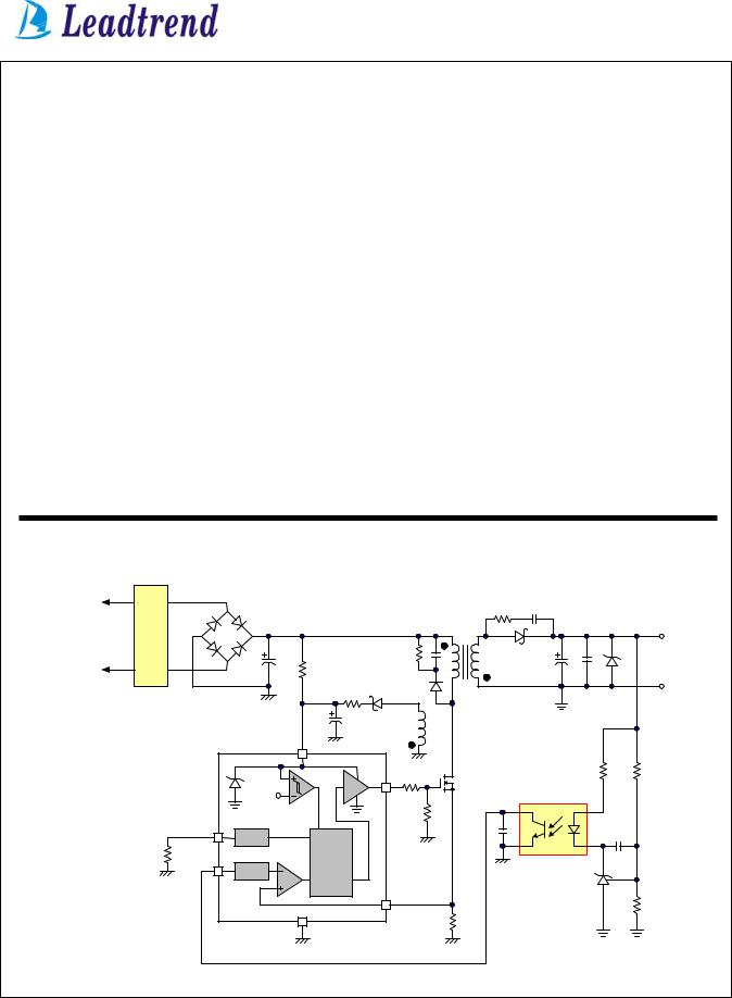
Leadtrend LD7535ABL, LD7535AGL, LD7535BL, LD7535GL, LD7535ABN Schematic [ru]
...
LD7535/LD7535A
12/11/2007
Green-Mode PWM Controller with Integrated Protections
Rev. 01c
General Description
The LD7535/LD7535A are low cost, low startup current, current mode PWM controllers with green-mode powersaving operation. The integrated functions include the leading-edge blanking of the current sensing, internal slope compensation and the tiny package of SOT-26. They provide the users a superior AC/DC power application of higher efficiency, low external component counts, and lower cost solution.
Furthermore, LD7535/LD7535A features more protections like OLP (Over Load Protection) and OVP (Over Voltage Protection) to eliminate the external protection circuits. And to satisfy different designs, 2 versions of OVP levels are implemented as ---
zLD7535 --- 28.0V ± 1.5V.
zLD7535A --- 21.0V ± 1.5V.
Features
zHigh-Voltage CMOS Process with Excellent ESD protection
zVery Low Startup Current (<20μA)
zCurrent Mode Control
zNon-audible-noise Green Mode Control
zUVLO (Under Voltage Lockout)
zLEB (Leading-Edge Blanking) on CS Pin
zProgrammable Switching Frequency
zInternal Slope Compensation
zOVP (Over Voltage Protection) on Vcc Pin
zOLP (Over Load Protection)
z300mA Driving Capability
Applications
zSwitching AC/DC Adaptor and Battery Charger
zOpen Frame Switching Power Supply
z384X Replacement
Typical Application
1
Leadtrend Technology Corporation www.leadtrend.com.tw
LD7535&LD7535A-DS-01c December 2007

LD7535/LD7535A
Pin Configuration (LD7535)
DIP-8 (TOP VIEW) |
SOT-26 (TOP VIEW) |
|||||||
GND |
COMP |
NC |
RT |
|
|
|
|
|
8 |
7 |
6 |
5 |
|
|
|
|
|
|
|
|
|
|
|
|
|
|
|
|
|
|
6 |
5 |
4 |
|
|
|
|
|
|
WP 35 |
|
|
||
|
TOP MARK |
|
Y |
|
|
|||
|
YYWW## |
|
1 |
2 |
3 |
|
||
|
|
|
|
|
|
|
||
1 |
2 |
3 |
4 |
OUT |
VCC |
NC |
CS |
YThe PB free package is identified in embossed font while green package in regular font.
YY, |
Y : |
Year code (D: 2004, E: 2005…..) |
WW, W: |
Week code |
|
P |
: |
LD75.. |
|
|
(Product family code) |
##: Production code
Pin Configuration (LD7535A)
DIP-8 (TOP VIEW) |
|
SOT-26 (TOP VIEW) |
||||||||
GND |
COMP |
NC |
RT |
|
|
|
|
|
|
|
8 |
7 |
6 |
5 |
|
|
|
|
|
|
|
|
|
|
|
|
|
|
|
|
|
|
|
|
|
|
|
|
6 |
5 |
4 |
|
|
|
|
|
|
|
WP 35A |
|
|
|||
TOP MARK |
|
|
|
Y |
|
|
||||
|
YYWW## |
|
|
|
1 |
2 |
3 |
|
||
|
|
|
|
|
|
|
|
|
||
1 |
2 |
3 |
4 |
Y |
|
The PB free package is identified |
||||
OUT |
VCC |
NC |
CS |
|
||||||
|
|
in embossed font while green |
||||||||
|
|
|
|
|
|
|||||
|
|
|
|
|
|
package in regular font. |
||||
YY, |
Y : Year code (D: 2004, E: 2005…..) |
|
|
|||||||
WW, W: Week code |
|
|
|
|
|
|
|
|||
P |
: |
LD75.. |
|
|
|
|
|
|
|
|
|
|
(Product family code) |
|
|
|
|
||||
##: Production code
Ordering Information
Part number |
|
Package |
TOP MARK |
Shipping |
||
LD7535 BL |
SOT-26 |
|
PB Free |
YWP/35 |
3000 |
/tape & reel |
LD7535 GL |
SOT-26 |
|
Green Package |
YWP/35 |
3000 |
/tape & reel |
LD7535 BN |
DIP-8 |
|
PB Free |
LD7535BN |
3600 |
/tube /Carton |
LD7535A BL |
SOT-26 |
|
PB Free |
YWP/35A |
3000 |
/tape & reel |
LD7535A GL |
SOT-26 |
|
Green Package |
YWP/35A |
3000 |
/tape & reel |
LD7535A BN |
DIP-8 |
|
PB Free |
LD7535ABN |
3600 |
/tube /Carton |
The LD7535/ LD7535A are ROHS Complaint/ Green Package.
2
Leadtrend Technology Corporation www.leadtrend.com.tw
LD7535&LD7535A-DS-01c December 2007

|
|
|
LD7535/LD7535A |
|
|
|
|
|
|
Pin Descriptions |
|
|
|
|
|
|
|
|
|
|
PIN |
NAME |
FUNCTION |
|
|
1 |
GND |
Ground |
|
|
2 |
COMP |
Voltage feedback pin (same as the COMP pin in UC384X), By connecting |
|
|
a photo-coupler to close the control loop and achieve the regulation. |
|
||
|
|
|
|
|
|
3 |
RT |
This pin is to program the switching frequency. By connecting a resistor |
|
|
to ground to set the switching frequency. |
|
||
|
|
|
|
|
|
4 |
CS |
Current sense pin, connect to sense the MOSFET current |
|
|
5 |
VCC |
Supply voltage pin |
|
|
6 |
OUT |
Gate drive output to drive the external MOSFET |
|
|
|
|
|
|
3
Leadtrend Technology Corporation www.leadtrend.com.tw
LD7535&LD7535A-DS-01c December 2007

LD7535/LD7535A
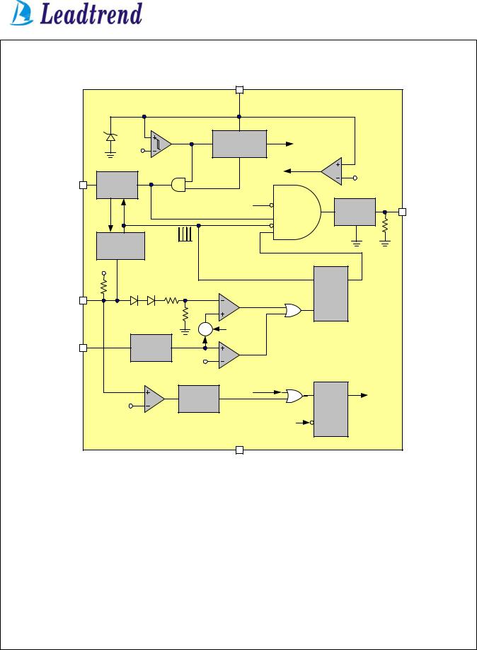
Block Diagram
∑ |
* Note: OLP delay is 60mS when the switching frequency is set as 65KHz. The OLP delay time is proportional to the period of switching cycle.
That is, |
T |
T = |
1 |
. |
|
||||
|
OLP _ delay |
s |
fs |
|
|
|
|
||
4
Leadtrend Technology Corporation www.leadtrend.com.tw
LD7535&LD7535A-DS-01c December 2007

|
LD7535/LD7535A |
|
|
Absolute Maximum Ratings |
|
Supply Voltage VCC |
30V |
COMP, RT, CS |
-0.3 ~7V |
Junction Temperature |
150°C |
Operating Ambient Temperature |
-40°C to 85°C |
Storage Temperature Range |
-65°C to 150°C |
Package Thermal Resistance (SOT-26) |
250°C/W |
Package Thermal Resistance (DIP-8) |
100°C/W |
Power Dissipation (SOT-26, at Ambient Temperature = 85°C) |
250mW |
Power Dissipation (DIP-8, at Ambient Temperature = 85°C) |
650mW |
Lead temperature (Soldering, 10sec) |
260°C |
ESD Voltage Protection, Human Body Model |
3KV |
ESD Voltage Protection, Machine Model |
250V |
Gate Output Current |
300mA |
Caution:
Stresses beyond the ratings specified in “Absolute Maximum Ratings” may cause permanent damage to the device. This is a stress only rating and operation of the device at these or any other conditions above those indicated in the operational sections of this specification is not implied.
Recommended Operating Conditions
Item |
Min. |
Max. |
Unit |
Supply Voltage Vcc (LD7535) |
11 |
25 |
V |
Supply Voltage Vcc (LD7535A) |
11 |
18 |
V |
Switching Frequency |
50 |
130 |
KHz |
Startup Resistor Value |
1.2 |
4.4 |
MΩ |
5
Leadtrend Technology Corporation www.leadtrend.com.tw
LD7535&LD7535A-DS-01c December 2007

LD7535/LD7535A
Electrical Characteristics
(TA = +25oC unless otherwise stated, VCC=15.0V)
PARAMETER |
CONDITIONS |
MIN |
TYP |
MAX |
UNITS |
|
Supply Voltage (Vcc Pin) |
|
|
|
|
|
|
Startup Current |
|
|
8 |
20 |
μA |
|
Operating Current |
VCOMP=0V |
|
2.0 |
3.0 |
mA |
|
VCOMP=3V |
|
2.5 |
|
mA |
||
(with 1nF load on OUT pin) |
|
|
||||
Protection tripped (OLP, OVP) |
|
0.5 |
|
mA |
||
|
|
|
||||
UVLO (off) |
|
9.0 |
10.0 |
11.0 |
V |
|
UVLO (on) |
|
15.0 |
16.0 |
17.0 |
V |
|
OVP Level |
LD7535 |
26.5 |
28.0 |
29.5 |
V |
|
LD7535A |
19.5 |
21.0 |
22.5 |
V |
||
|
||||||
Voltage Feedback (Comp Pin) |
|
|
|
|
|
|
Short Circuit Current |
VCOMP=0V |
|
1.5 |
2.2 |
mA |
|
Open Loop Voltage |
COMP pin open |
|
6.0 |
|
V |
|
Green Mode Threshold VCOMP |
|
|
2.35 |
|
V |
|
Current Sensing (CS Pin) |
|
|
|
|
|
|
Maximum Input Voltage, Vcs(off) |
|
0.80 |
0.85 |
0.90 |
V |
|
Leading Edge Blanking Time |
|
|
350 |
|
nS |
|
Input impedance |
|
1 |
|
|
MΩ |
|
Delay to Output |
|
|
100 |
|
nS |
|
Oscillator (RT pin) |
|
|
|
|
|
|
Frequency |
RT=100KΩ |
60 |
65 |
70 |
KHz |
|
Green Mode Frequency |
Fs=65KHz |
|
20 |
|
KHz |
|
Temp. Stability |
(-40°C ~105°C) |
|
|
3 |
% |
|
Voltage Stability |
(VCC=11V-25V) |
|
|
1 |
% |
|
Gate Drive Output (OUT Pin) |
|
|
|
|
|
|
Output Low Level |
VCC=15V, Io=20mA |
|
|
1 |
V |
|
Output High Level |
VCC=15V, Io=20mA |
8 |
|
|
V |
|
Rising Time |
Load Capacitance=1000pF |
|
50 |
200 |
nS |
|
Falling Time |
Load Capacitance=1000pF |
|
30 |
100 |
nS |
|
OLP (Over Load Protection) |
|
|
|
|
|
|
OLP Trip Level |
VCOMP(OLP) |
|
5.0 |
|
V |
|
OLP Delay Time (note) |
Fs=65KHz |
|
60 |
|
mS |
Note: The OLP delay time is proportional to the period of switching cycle. So that, the lower RT value will set the higher switching frequency and the shorter OLP delay time.
6
Leadtrend Technology Corporation www.leadtrend.com.tw
LD7535&LD7535A-DS-01c December 2007
 Loading...