


 Loading...
Lattice Semiconductor Corporation PALCE16V8H-10JC-4, PALCE16V8Q-15PC-4, PALCE16V8Q-20JI-4, PALCE16V8Q-20PI-4, PALCE16V8H-15SC-4 Datasheet
...
|
|
|
|
|
PALCE16V8 |
COM’L:H-5/7/10/15/25, Q-10/15/25 IND:H-10/15/25, Q-20/25 |
|
|
|
|
|
|
PALCE16V8Z |
COM’L:-25 |
IND:-12/15/25 |
|
|
|
|
|
|
|
|
|
|
|
|
|
|
|
|
|
|
|
|
|
|
|
|
|
|
|
|
|
|
|
|
PALCE16V8 and PALCE16V8Z Families
EE CMOS (Zero-Power) 20-Pin Universal
Programmable Array Logic
DISTINCTIVE CHARACTERISTICS
Pin and function compatible with all 20-pin PAL® devices
Electrically erasable CMOS technology provides reconfigurable logic and full testabilityHigh-speed CMOS technology
— 5-ns propagation delay for “-5” version
— 7.5-ns propagation delay for “-7” version
Direct plug-in replacement for the PAL16R8 series
Outputs programmable as registered or combinatorial in any combination
Peripheral Component Interconnect (PCI) compliant |
FOR |
|
Programmable output polarity |
||
|
||
Programmable enable/disable control |
|
|
Preloadable output registers for testability |
|
|
Automatic register reset on power up |
|
|
DEVICES |
|
|
Cost-effective 20-pin plastic DIP, PLCC, and SOIC packages |
|
|
Extensive third-party software and programmer support |
|
|
DESIGNS |
||
Fully tested for 100% programming and functional yields and high reliability5-ns version utilizes a split leadframe for improved performance
The PALCE16V8 is an advanced PAL device built with low-power, high-speed, electrically- |
|
erasable CMOS technology. It is functionally compatible with all 20-pin GAL devices. The |
|
|
GAL |
macrocells provide a universal device architecture. The PALCE16V8 will directly replace the |
|
PAL16R8, with the exception of the PAL16C1. |
|
|
NEW |
The PALCE16V8Z provides zero standby power and high speed. At 30-µA maximum standby |
|
current, the PALCE16V8Z allows battery-powered operation for an extended period. |
|
USE |
|
The PALCE16V8 utilizes the familiar sum-of-products (AND/OR) architecture that allows users to implement complex logic functions easily and efficiently. Multiple levels of combinatorial logic can always be reduced to sum-of-products form, taking advantage of the very wide input gates available in PAL devices. The equations are programmed into the device through floating-gate cells in the AND logic array that can be erased electrically.
The fixed OR array allows up to eight data product terms per output for logic functions. The sum of these products feeds the output macrocell. Each macrocell can be programmed as registered or combinatorial with an active-high or active-low output. The output configuration is determined by two global bits and one local bit controlling four multiplexers in each macrocell.
Publication# 16493 |
Rev: F |
Amendment/0 |
Issue Date: September 2000 |
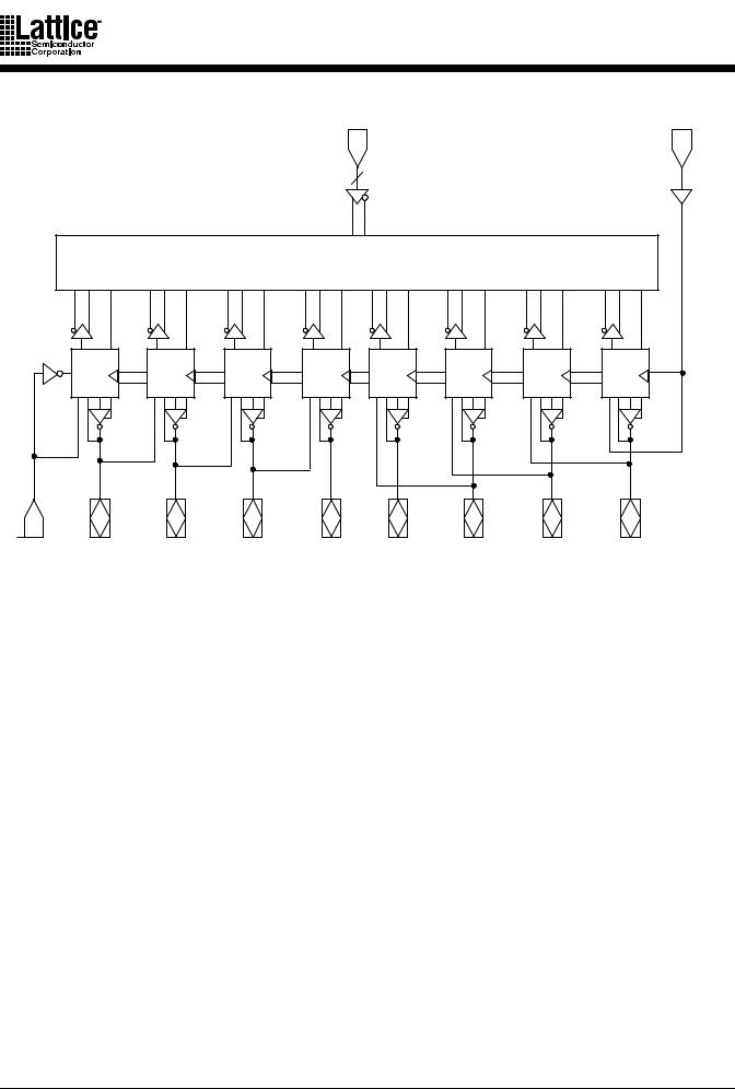
BLOCK DIAGRAM
I1 – I8 |
CLK/I0 |
8 |
|
Programmable AND Array
32 x 64
MACRO |
MACRO |
MACRO |
MACRO |
MACRO |
|
|
FOR |
MACRO |
|||||
MACRO |
MACRO |
||||||||||||
MC0 |
MC |
MC |
2 |
MC |
MC |
4 |
MC |
5 |
|
MC |
6 |
MC |
7 |
|
1 |
|
3 |
|
|
|
|
|
|||||
OE/I9 I/O0 I/O1 I/O2 I/O3 I/O4 I/O5 I/O6 I/O7 16493E-1
FUNCTIONAL DESCRIPTION |
DEVICES |
|
The PALCE16V8 is a universal PAL device. The PALCE16V8Z is the zero-power version of the |
|
GAL |
DESIGNS |
PALCE16V8. It has all the architectural features of the PALCE16V8. In addition, the PALCE16V8Z has zero standby power and an unusedNEWproduct term disable feature for reduced power consumption. It has eight independently configurable macrocells (MC0-MC7). Each macrocell can be configured as registeredUSEoutput, combinatorial output, combinatorial I/O or dedicated input. The programming matrix implements a programmable AND logic array, which drives a fixed OR logic array. Buffers for device inputs have complementary outputs to provide userprogrammable input signal polarity. Pins 1 and 11 serve either as array inputs or as clock (CLK) and output enable (OE), respectively, for all flip-flops.
Unused input pins should be tied directly to VCC or GND. Product terms with all bits unprogrammed (disconnected) assume the logical HIGH state, and product terms with both true and complement of any input signal connected assume a logical LOW state.
The programmable functions on the PALCE16V8 are automatically configured from the user’s design specification. The design specification is processed by development software to verify the design and create a programming file (JEDEC). This file, once downloaded to a programmer, configures the device according to the user’s desired function.
The user is given two design options with the PALCE16V8. First, it can be programmed as a standard PAL device from the PAL16R8 series. The PAL programmer manufacturer will supply device codes for the standard PAL device architectures to be used with the PALCE16V8. The programmer will program the PALCE16V8 in the corresponding architecture. This allows the user to use existing standard PAL device JEDEC files without making any changes to them.
2 |
PALCE16V8 and PALCE16V8Z Families |

Alternatively, the device can be programmed as a PALCE16V8. Here the user must use the PALCE16V8 device code. This option allows full utilization of the macrocell.
|
|
|
|
|
To |
|
|
|
|
|
Adjacent |
|
|
|
|
1 1 |
Macrocell |
|
|
|
OE |
|
|
1 1 |
|
|
1 0 |
|
|
0 X |
|
VCC |
0 0 |
|
|
|
0 1 |
|
|||
1 0 |
|
|
|
|
|
|
SL0X |
|
|
|
|
SG1 |
|
|
|
1 1 |
|
|
|
|
|
|
|
|
|
|
|
0 X |
I/OX |
|
D |
Q |
|
1 0 |
|
|
|
|
|||
SL1X |
CLK |
Q |
FOR |
|
|
|
|
|
|
||
|
|
|
|
1 0 |
|
|
|
|
|
1 1 |
|
|
|
|
|
0 X |
From |
|
|
|
*SG1 |
SL0X |
Adjacent |
*In macrocells MC0 and MC7, SG1 is replaced by SG0 on the feedback multiplexer. |
Pin |
||||
|
|
|
|||
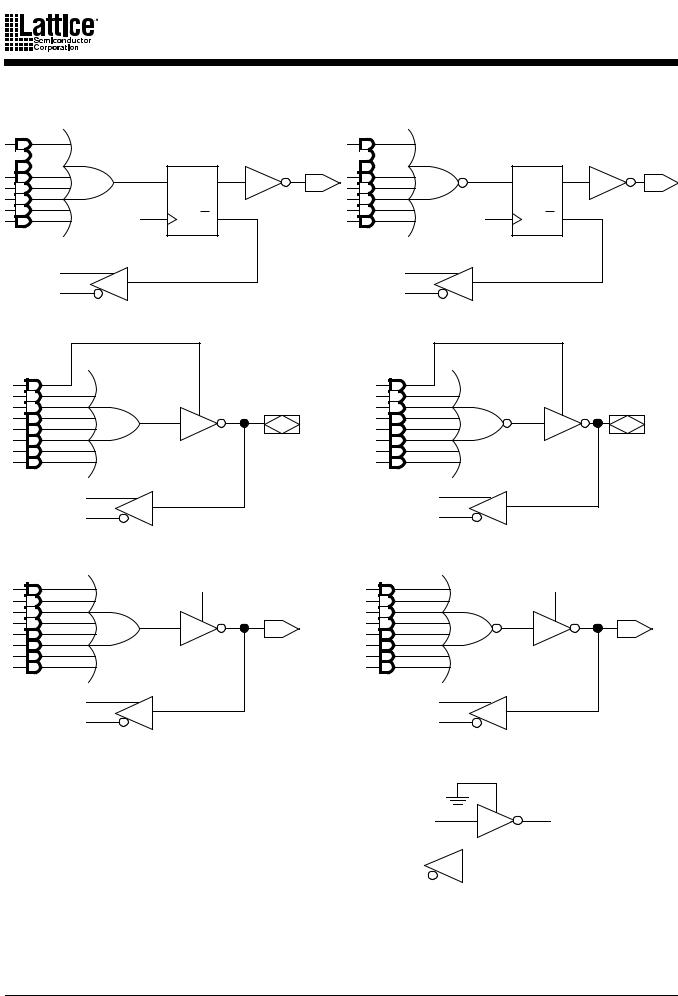
Figure 1. PALCE16V8 Macrocell |
|
|
16493E-2 |
||
|
|
|
|||
CONFIGURATION OPTIONS |
DEVICES |
|
|
|
|
Each macrocell can be configured as one of theDESIGNSfollowing: registered output, combinatorial output, combinatorial I/O, or dedicated input. In the registered output configuration, the output
buffer is enabled by the OE pin.GALIn the combinatorial configuration, the buffer is either controlled by a product term or always enabled. In the dedicated input configuration, it is always disabled.
The macrocell configurationsUSE |
are controlled by the configuration control word. It contains 2 |
With the exception of MC0 and MC7, a macrocell configured as a dedicated input derives the
input signal from an adjacent I/O. MC0 |
derives its input from pin 11 (OE) and MC7 from pin 1 |
|
(CLK). |
NEW |
|
|
|
|
global bits (SG0 and SG1) and 16 local bits (SL00 through SL07 and SL10 through SL17). SG0 determines whether registers will be allowed. SG1 determines whether the PALCE16V8 will emulate a PAL16R8 family or a PAL10H8 family device. Within each macrocell, SL0x, in conjunction with SG1, selects the configuration of the macrocell, and SL1x sets the output as either active low or active high for the individual macrocell.
The configuration bits work by acting as control inputs for the multiplexers in the macrocell. There are four multiplexers: a product term input, an enable select, an output select, and a feedback select multiplexer. SG1 and SL0x are the control signals for all four multiplexers. In MC0 and MC7, SG0 replaces SG1 on the feedback multiplexer. This accommodates CLK being the adjacent pin for MC7 and OE the adjacent pin for MC0.
PALCE16V8 and PALCE16V8Z Families |
3 |

Registered Output Configuration
The control bit settings are SG0 = 0, SG1 = 1 and SL0x = 0. There is only one registered configuration. All eight product terms are available as inputs to the OR gate. Data polarity is determined by SL1x. The flip-flop is loaded on the LOW-to-HIGH transition of CLK. The feedback path is from Q on the register. The output buffer is enabled by OE.
Combinatorial Configurations
The PALCE16V8 has three combinatorial output configurations: dedicated output in a nonregistered device, I/O in a non-registered device and I/O in a registered device.
Dedicated Output in a Non-Registered Device
The control bit settings are SG0 = 1, SG1 = 0 and SL0x = 0. All eight product terms are available to the OR gate. Although the macrocell is a dedicated output, the feedback is used, with the exception of pins 15 and 16. Pins 15 and 16 do not use feedback in this mode. Because CLK
and OE are not used in a non-registered device, pins 1 and 11 are available as input signals. Pin |
|
1 will use the feedback path of MC7, and pin 11 will use the feedback path of MC0. |
|
Combinatorial I/O in a Non-Registered Device |
FOR |
Combinatorial I/O in a Registered DeviceDEVICES
The control bit settings are SG0 = 1, SG1 = 1, and SL0x = 1. Only seven product terms are available to the OR gate. The eighth product term is used to enable the output buffer. The signal at the I/O pin is fed back to the AND array via the feedback multiplexer. This allows the pin to be used as an input.
Because CLK and OE are not used in a non-registered device, pins 1 and 11 are available as inputs. Pin 1 will use the feedback path of MC7, and pin 11 will use the feedback path of MC0.
The control bit settings are SG0 = 1, SG1 = 0 and SL0x = 1. The output buffer is disabled. Except for MC0 and MC7, the feedback signal is an adjacent I/O. For MC0 and MC7, the feedback signals are pins 1 and 11. These configurations are summarized in Table 1 and illustrated in Figure 2.
The control bit settings are SG0 = 0, SG1 = 1 and SL0x = 1. Only seven product terms are available |
|||
|
|
|
DESIGNS |
to the OR gate. The eighth product term is used as the output enable. The feedback signal is the |
|||
corresponding I/O signal. |
GAL |
|
|
|
|
||
Dedicated Input Configuration |
NEW |
|
|
USE |
|
|
|
|
|
|
|
|
|
|
Cell |
Devices |
|
|
|
Cell |
Devices |
|
SG0 |
SG1 |
SL0X |
Configuration |
Emulated |
SG0 |
SG1 |
SL0X |
Configuration |
Emulated |
|
|
|
Device Uses Registers |
|
|
|
Device Uses No Registers |
|
|||
|
|
|
|
|
|
|
|
|
|
|
|
|
|
|
PAL16R8, 16R6, |
|
|
|
Combinatorial |
PAL10H8, 12H6, |
|
0 |
1 |
0 |
Registered Output |
1 |
0 |
0 |
14H4, 16H2, 10L8, |
|||
16R4 |
Output |
|||||||||
|
|
|
|
|
|
|
12L6, 14L4, 16L2 |
|||
|
|
|
|
|
|
|
|
|
||
|
|
|
|
|
|
|
|
|
|
|
|
|
|
Combinatorial |
|
|
|
|
|
PAL12H6, 14H4, |
|
0 |
1 |
1 |
PAL16R6, 16R4 |
1 |
0 |
1 |
Input |
16H2, 12L6, 14L4, |
||
I/O |
||||||||||
|
|
|
|
|
|
|
|
16L2 |
||
|
|
|
|
|
|
|
|
|
||
|
|
|
|
|
|
|
|
|
|
|
|
|
|
|
|
1 |
1 |
1 |
Combinatorial |
PAL16L8 |
|
|
|
|
|
|
I/O |
|||||
|
|
|
|
|
|
|
|
|
||
|
|
|
|
|
|
|
|
|
|
|
4 |
PALCE16V8 and PALCE16V8Z Families |

Programmable Output Polarity
The polarity of each macrocell can be active-high or active-low, either to match output signal needs or to reduce product terms. Programmable polarity allows Boolean expressions to be written in their most compact form (true or inverted), and the output can still be of the desired polarity. It can also save “DeMorganizing” efforts.
Selection is through a programmable bit SL1x which controls an exclusive-OR gate at the output of the AND/OR logic. The output is active high if SL1x is 1 and active low if SL1x is 0.
|
|
DEVICES |
FOR |
|
|
GAL |
|
||
|
|
DESIGNS |
||
USE |
NEW |
|
|
|
|
|
|
|
|
PALCE16V8 and PALCE16V8Z Families |
5 |
|
|
|
OE |
|
|
|
|
|
|
|
OE |
|
|
|
|
|
|
|
|
||||||||||
|
|
|
|
|
|
|
|
|
|
|
|
|
|
|
|
|
|
|
|
|
|
|
|
|
|
|
|
|
|
|
|
|
|
|
|
|
|
|
|
|
|
|
|
|
D |
Q |
D |
Q |
CLK |
Q |
CLK |
Q |
a. Registered active low |
|
|
|
|
FOR |
|
|
|
|
b. Registered active high |
|||
|
GAL |
DEVICES |
|
|
||
|
|
DESIGNS |
|
|||
c. Combinatorial I/O active low |
|
|
d. Combinatorial I/O active high |
|||
VCC |
NEW |
|
|
VCC |
||
USE |
|
|
|
|
||
|
Note 1 |
|
|
|
Note 1 |
|
|
|
|
|
|
||
e. Combinatorial output active low |
|
f. Combinatorial output active high |
||||
Notes:
1.Feedback is not available on pins 15 and 16 in the combinatorial output mode.
2.This configuration is not available on pins 15 and 16.
 Adjacent I/O pin Note 2
g. Dedicated input
16493E-2
Figure 2. Macrocell Configurations
6 |
PALCE16V8 and PALCE16V8Z Families |

Power-Up Reset
All flip-flops power up to a logic LOW for predictable system initialization. Outputs of the PALCE16V8 will depend on whether they are selected as registered or combinatorial. If registered is selected, the output will be HIGH. If combinatorial is selected, the output will be a function of the logic.
Register Preload
The register on the PALCE16V8 can be preloaded from the output pins to facilitate functional testing of complex state machine designs. This feature allows direct loading of arbitrary states, making it unnecessary to cycle through long test vector sequences to reach a desired state. In addition, transitions from illegal states can be verified by loading illegal states and observing proper recovery.
Security Bit FOR
A security bit is provided on the PALCE16V8 as a deterrent to unauthorized copying of the array configuration patterns. Once programmed, this bit defeats readback and verification of the programmed pattern by a device programmer,DEVICESsecuring proprietary designs from competitors. The bit can only be erased in conjunction with the array during an erase cycle.
Electronic Signature Word DESIGNS
An electronic signature word is provided in the PALCE16V8 device. It consists of 64 bits of programmable memory that can contain user-defined data. The signature data is always available to the user independent of the security bit.
Programming and Erasing
The PALCE16V8 can be programmed on standard logic programmers. It also may be erased to reset a previously configured device back to its unprogrammed state. Erasure is automatically performed by the programming hardware. No special erase operation is required.
GAL The PALCE16V8 offers a very high level of built-in quality. The erasability of the device provides
Quality and Testability
a direct means of verifying performance of all AC and DC parameters. In addition, this verifies |
|
complete programmability and functionalityNEWof the device to provide the highest programming |
|
yields and post-programming functional yields in the industry. |
|
Technology |
USE |
|
|
The high-speed PALCE16V8 is fabricated with Vantis’ advanced electrically-erasable (EE) CMOS process. The array connections are formed with proven EE cells. Inputs and outputs are designed to be compatible with TTL devices. This technology provides strong input clamp diodes, output slew-rate control, and a grounded substrate for clean switching.
PCI Compliance
PALCE16V8 devices in the -5/-7/-10 speed grades are fully compliant with the PCI Local Bus Specification published by the PCI Special Interest Group. The PALCE16V8’s predictable timing ensures compliance with the PCI AC specifications independent of the design.
Zero-Standby Power Mode
The PALCE16V8Z features a zero-standby power mode. When none of the inputs switch for an extended period (typically 50 ns), the PALCE16V8Z will go into standby mode, shutting down
PALCE16V8 and PALCE16V8Z Families |
7 |

most of its internal circuitry. The current will go to almost zero (ICC < 15 µA). The outputs will maintain the states held before the device went into the standby mode. There is no speed penalty associated with coming out of standby mode.
When any input switches, the internal circuitry is fully enabled, and power consumption returns to normal. This feature results in considerable power savings for operation at low to medium frequencies. This saving is illustrated in the ICC vs. frequency graph.
Product-Term Disable
On a programmed PALCE16V8Z, any product terms that are not used are disabled. Power is cut off from the product terms so that they do not draw current. As shown in the ICC vs. frequency graph, product-term disabling results in considerable power savings. This saving is greater at the
higher frequencies. |
|
|
|
FOR |
|
|
|
|
|
Further hints on minimizing power consumption can be found in a separate document entitled, |
||||
Minimizing Power Consumption with Zero-Power PLDs. |
|
|||
|
GAL |
DEVICES |
|
|
|
|
DESIGNS |
||
USE |
NEW |
|
|
|
|
|
|
|
|
8 |
PALCE16V8 and PALCE16V8Z Families |

LOGIC DIAGRAM
|
0 |
3 |
4 |
7 |
8 |
11 12 |
15 16 |
19 |
20 |
23 24 |
27 28 |
31 |
|
|
|
|
|
|
|
|
|
CLK/I0 |
1 |
|
|
|
|
|
|
|
|
|
|
|
|
|
|
|
|
|
|
|
|
|
|
|
|
|
|
|
|
|
|
|
|
|
1 1 |
|
|
|
|
|
1 1 |
20 VCC |
|
|
|
|
|
|
|
|
|
|
|
|
|
|
|
|
|
|
|
1 0 |
|
|
|
|
|
|
|
|
|
|
|
|
|
|
|
|
0 X |
|
|
|
|
VCC |
0 0 |
|
|
|
|
|
|
|
|
|
|
|
|
|
|
|
|
|
|
|
|
0 1 |
|
|
|
|
|
|
|
|
|
|
|
|
|
|
|
|
1 0 |
|
|
|
|
|
|
|
|
|
0 |
|
|
|
|
|
|
|
|
|
|
|
|
|
|
SL07 |
|
|
|
|
|
|
|
|
|
|
|
|
|
|
|
|
|
|
SG1 |
|
|
|
|
|
|
|
|
|
|
|
|
|
|
|
|
|
|
|
|
|
|
|
|
|
|
1 1 |
|
|
|
|
|
|
|
|
|
|
|
|
|
|
|
|
|
|
|
|
|
|
|
|
|
|
|
|
|
|
|
|
|
|
|
|
|
|
|
|
|
|
|
|
0 X |
19 |
I/O7 |
|
|
|
|
|
|
|
|
|
|
|
|
|
|
|
|
|
D |
Q |
1 0 |
||
|
7 |
|
|
|
|
|
|
|
|
|
|
|
|
SL17 |
|
|
Q |
|
|
|
|
|
|
|
|
|
|
|
|
|
|
|
|
|
|
|
|
|
|
|
|
||
|
|
|
|
|
|
|
|
|
|
|
|
|
|
|
FOR |
|
1 0 |
|
|
||
I1 |
2 |
|
|
|
|
|
|
|
|
|
|
|
|
|
|
1 1 |
|
|
|||
|
|
|
|
|
|
|
|
|
|
|
|
|
|
0 X |
|
|
|||||
|
|
|
|
|
|
|
|
|
|
|
|
|
|
|
SG0 |
|
SL0 7 |
|
|||
|
|
|
|
|
|
|
|
|
|
|
|
|
|
|
|
1 1 |
|
|
|||
|
|
|
|
|
|
|
|
|
|
|
|
|
1 1 |
|
|
1 0 |
|
|
|||
|
|
|
|
|
|
|
|
|
|
|
|
|
0 X |
|
VCC |
0 0 |
|
|
|||
|
|
|
|
|
|
|
|
|
|
|
|
|
|
|
0 1 |
|
|
||||
|
|
|
|
|
|
|
|
|
|
|
|
|
1 0 |
|
|
|
|
|
|||
|
|
|
|
|
|
|
|
|
|
|
|
|
|
|
|
|
|
|
|||
|
8 |
|
|
|
|
|
|
|
|
|
|
|
|
|
|
SL06 |
|
|
|
|
|
|
|
|
|
|
|
|
|
|
|
|
|
|
SG1 |
|
|
|
|
1 1 |
|
|
|
|
|
|
|
|
|
|
|
|
|
|
|
|
|
|
|
|
|
|
|
||
|
|
|
|
|
|
|
|
|
|
|
|
|
|
|
|
|
|
|
|
|
|
|
|
|
|
|
|
|
|
|
|
|
|
|
|
|
|
|
|
|
0 X |
18 |
I/O6 |
|
|
|
|
|
|
|
|
|
|
|
|
|
|
|
|
|
D |
Q |
1 0 |
||
|
|
|
|
|
|
|
|
|
|
|
|
|
|
|
|
|
|
|
|||
|
15 |
|
|
|
|
|
|
|
|
|
|
|
|
SL16 |
|
|
Q |
|
|
|
|
|
|
|
|
|
|
|
|
|
|
|
|
|
|
|
|
|
|
|
|
||
|
|
|
|
|
|
|
|
|
|
|
|
|
|
|
|
|
|
|
1 0 |
|
|
I2 |
3 |
|
|
|
|
|
|
|
|
|
|
|
|
|
|
|
|
|
1 1 |
|
|
|
|
|
|
|
|
|
|
|
|
|
|
|
|
|
|
|
0 X |
|
|
||
|
|
|
|
|
|
|
|
|
|
|
|
|
|
|
|
|
|
SG1 |
|
SL0 6 |
|
|
|
|
|
|
|
|
|
|
|
|
|
|
|
|
|
|
|
|
1 1 |
|
|
|
|
|
|
|
|
|
|
|
|
|
|
|
1 1 |
|
|
|
|
|
1 0 |
|
|
|
|
|
|
|
|
|
|
|
|
|
|
|
0 X |
|
|
|
|
VCC |
0 0 |
|
|
|
|
|
|
|
|
|
|
|
|
|
|
|
|
|
|
|
|
0 1 |
|
|
|
|
|
|
|
|
|
|
|
|
|
|
DEVICES |
|
|
|
|
|
|
|
|||
|
|
|
|
|
|
|
|
|
|
|
|
|
1 0 |
|
|
|
|
|
|
|
|
|
|
|
|
|
|
|
|
|
|
|
|
|
|
|
|
SL05 |
|
|
|
|
|
|
16 |
|
|
|
|
|
GAL |
|
DESIGNSSG1 |
|
|
1 1 |
|
|
|||||||
|
|
|
|
|
|
|
|
|
|
|
|
|
|
|
0 X |
17 I/O5 |
|||||
|
|
|
|
|
|
|
|
|
|
|
|
|
D |
Q |
1 0 |
||||||
|
|
|
|
|
|
|
|
|
|
|
|
|
|
|
|||||||
|
23 |
|
|
|
|
|
|
|
|
SL15 |
|
|
Q |
|
|
|
|||||
|
|
|
|
|
|
|
|
|
|
|
|
|
|
|
|
||||||
|
|
|
USE |
|
|
NEW |
|
|
|
|
|
|
|
1 0 |
|
|
|||||
I3 |
4 |
|
|
|
|
|
|
|
|
|
|
1 1 |
|
|
|||||||
|
|
|
|
|
|
|
|
|
|
0 X |
|
|
|||||||||
|
|
|
|
|
|
|
|
|
|
|
SG1 |
|
SL0 5 |
|
|||||||
|
|
|
|
|
|
|
|
|
|
|
|
|
|
|
|||||||
|
|
|
|
|
|
|
|
|
|
|
|
|
|
|
1 1 |
|
|
||||
|
|
|
|
|
|
|
|
|
1 1 |
|
|
|
|
|
1 0 |
|
|
||||
|
|
|
|
|
|
|
|
|
|
|
|
|
0 X |
|
|
|
|
VCC |
0 0 |
|
|
|
|
|
|
|
|
|
|
|
|
|
|
|
|
|
|
|
|
0 1 |
|
|
|
|
|
|
|
|
|
|
|
|
|
|
|
|
1 0 |
|
|
|
|
|
|
|
|
|
24 |
|
|
|
|
|
|
|
|
|
|
|
|
|
|
SL04 |
|
|
|
|
|
|
|
|
|
|
|
|
|
|
|
|
|
|
SG1 |
|
|
|
1 1 |
|
|
||
|
|
|
|
|
|
|
|
|
|
|
|
|
|
|
|
|
|
|
|
|
|
|
|
|
|
|
|
|
|
|
|
|
|
|
|
|
|
|
|
|
0 X |
16 I/O4 |
|
|
|
|
|
|
|
|
|
|
|
|
|
|
|
|
|
|
D |
Q |
1 0 |
||
|
|
|
|
|
|
|
|
|
|
|
|
|
|
|
|
|
|
|
|||
|
31 |
|
|
|
|
|
|
|
|
|
|
|
|
SL14 |
|
|
Q |
|
|
|
|
|
|
|
|
|
|
|
|
|
|
|
|
|
|
|
|
|
|
|
|
||
|
|
|
|
|
|
|
|
|
|
|
|
|
|
|
|
|
|
|
1 0 |
|
|
I4 |
5 |
|
|
|
|
|
|
|
|
|
|
|
|
|
|
|
|
|
1 1 |
|
|
|
|
|
|
|
|
|
|
|
|
|
|
|
|
|
|
|
0 X |
|
|
||
|
|
|
|
|
|
|
|
|
|
|
|
|
|
|
|
|
|
SG1 |
|
SL0 4 |
|
|
0 |
3 |
4 |
7 |
8 |
11 12 |
15 16 |
19 20 |
23 24 |
27 28 |
31 |
|
|
|
CLK OE |
|
|
|
|
|
|
|
|
|
|
|
|
|
|
|
|
|
|
|
|
|
|
|
|
|
|
16493E-2 |
|
PALCE16V8 and PALCE16V8Z Families |
9 |
LOGIC DIAGRAM (CONTINUED) |
|
|
|
|
|
|
|
|
||||||||||||
|
0 |
3 |
4 |
7 |
8 |
11 12 |
15 |
16 |
19 |
20 |
23 24 |
27 28 |
31 |
CLK OE |
|
|
|
|
||
|
|
|
|
|
|
|
|
|
|
|
|
|
|
|
|
|
|
|
1 1 |
|
|
|
|
|
|
|
|
|
|
|
|
|
|
|
|
1 1 |
|
|
|
1 0 |
|
|
|
|
|
|
|
|
|
|
|
|
|
|
|
|
0 X |
|
|
VCC |
0 0 |
|
|
|
|
|
|
|
|
|
|
|
|
|
|
|
|
|
|
|
0 1 |
|
|
|
|
|
|
|
|
|
|
|
|
|
|
|
|
|
1 0 |
|
|
|
|
|
|
32 |
|
|
|
|
|
|
|
|
|
|
|
|
|
|
SL03 |
|
|
|
|
|
|
|
|
|
|
|
|
|
|
|
|
|
|
SG1 |
|
|
|
|
|
|
|
|
|
|
|
|
|
|
|
|
|
|
|
|
|
|
|
|
1 1 |
|
|
|
|
|
|
|
|
|
|
|
|
|
|
|
|
|
|
|
|
|
|
|
|
|
|
|
|
|
|
|
|
|
|
|
|
|
|
|
|
|
|
0 X |
|
|
|
|
|
|
|
|
|
|
|
|
|
|
|
|
|
|
D |
Q |
15 I/O 3 |
|
|
|
|
|
|
|
|
|
|
|
|
|
|
|
|
|
|
1 0 |
|
||
|
39 |
|
|
|
|
|
|
|
|
|
|
|
|
|
SL13 |
|
|
Q |
|
|
|
|
|
|
|
|
|
|
|
|
|
|
|
|
|
|
|
|
|
|
|
|
|
|
|
|
|
|
|
|
|
|
|
|
|
|
|
|
|
|
1 0 |
|
I 5 |
6 |
|
|
|
|
|
|
|
|
|
|
|
|
|
|
|
|
|
1 1 |
|
|
|
|
|
|
|
|
|
|
|
|
|
|
|
|
|
|
0 X |
|
||
|
|
|
|
|
|
|
|
|
|
|
|
|
|
|
|
|
|
SG1 |
SL0 3 |
|
|
|
|
|
|
|
|
|
|
|
|
|
|
|
|
|
FOR |
1 1 |
|
||
|
|
|
|
|
|
|
|
|
|
|
|
|
|
|
1 1 |
|
|
|
1 0 |
|
|
|
|
|
|
|
|
|
|
|
|
|
|
|
|
0 X |
|
|
VCC |
0 0 |
|
|
|
|
|
|
|
|
|
|
|
|
|
|
|
|
|
|
|
0 1 |
|
|
|
|
|
|
|
|
|
|
|
|
|
|
|
|
|
1 0 |
|
|
|
|
|
|
40 |
|
|
|
|
|
|
|
|
|
|
|
|
|
|
SL02 |
|
|
|
|
|
|
|
|
|
|
|
|
|
|
|
|
|
|
SG1 |
|
|
|
|
|
|
|
|
|
|
|
|
|
|
|
|
|
|
|
|
|
|
|
|
1 1 |
|
|
|
|
|
|
|
|
|
|
|
|
|
|
|
|
|
|
|
|
|
|
|
|
|
|
|
|
|
|
|
|
|
|
|
|
|
|
|
|
|
|
0 X |
I/O2 |
|
|
|
|
|
|
|
|
|
|
|
|
|
DEVICES |
|
D |
Q |
14 |
|||
|
|
|
|
|
|
|
|
|
|
|
|
|
|
1 0 |
|
|||||
|
|
|
|
|
|
|
|
|
|
|
|
|
|
|
|
|
|
|||
|
47 |
|
|
|
|
|
|
|
|
|
|
|
|
|
SL12 |
|
|
Q |
|
|
|
|
|
|
|
|
|
|
|
|
|
|
|
|
|
|
|
|
|
|
|
I7 |
8 |
|
|
|
|
|
|
|
|
|
|
|
|
|
DESIGNS |
|
|
1 0 |
|
|
|
|
|
|
|
|
|
|
|
|
|
|
|
|
|
0 X |
|
||||
I 6 |
7 |
|
|
|
|
|
|
|
|
|
|
|
|
|
|
|
|
|
1 1 |
|
|
|
|
|
|
|
|
|
|
|
|
|
|
|
|
|
|
0 X |
|
||
|
|
|
|
|
|
|
|
|
|
|
|
|
|
|
|
|
|
SG1 |
SL02 |
|
|
|
|
|
|
|
|
|
|
|
|
|
|
|
|
|
|
|
|
1 1 |
|
|
|
|
|
|
|
|
|
|
|
|
|
|
|
|
1 1 |
|
|
|
1 0 |
|
|
|
|
|
|
|
|
|
|
|
|
|
|
|
|
0 X |
|
|
VCC |
0 0 |
|
|
|
|
|
|
|
|
|
|
|
|
|
|
|
|
|
|
|
0 1 |
|
|
|
|
|
|
|
|
|
|
|
|
|
|
|
|
|
1 0 |
|
|
|
|
|
|
48 |
|
|
|
|
|
|
|
|
|
|
|
|
|
|
SL01 |
|
|
|
|
|
|
|
|
|
|
|
|
|
|
|
|
|
|
SG1 |
|
|
|
|
|
|
|
|
|
|
|
|
|
|
|
|
|
|
|
|
|
|
|
|
1 1 |
|
|
|
|
|
|
|
|
|
|
|
|
|
|
|
|
|
|
|
|
|
|
|
|
|
|
|
|
|
|
|
GAL |
|
|
|
|
|
|
0 X |
|
||||
|
|
|
|
|
|
|
|
|
|
|
|
D |
Q |
13 |
I/O1 |
|||||
|
|
|
|
|
|
|
|
|
|
|
|
|
|
|
|
|
1 0 |
|
||
|
55 |
|
|
|
|
|
|
|
|
|
|
|
|
|
SL11 |
|
|
Q |
|
|
|
|
|
|
|
|
|
|
|
|
|
|
|
|
|
|
|
|
|
|
|
|
|
|
|
|
|
|
|
|
|
NEW |
|
|
|
|
1 0 |
|
||||
|
|
|
|
|
|
|
|
|
|
|
|
|
|
1 1 |
|
|||||
|
|
|
USE |
|
|
|
|
|
|
|
|
|
|
SG1 |
SL0 1 |
|
||||
|
|
|
|
|
|
|
|
|
|
|
|
|
|
12 |
I/O 0 |
|||||
|
|
|
|
|
|
|
|
|
|
|
|
|
|
|
|
|
|
|
1 1 |
|
|
|
|
|
|
|
|
|
|
|
|
|
|
|
|
1 1 |
|
|
|
1 0 |
|
|
|
|
|
|
|
|
|
|
|
|
|
|
|
|
0 X |
|
|
VCC |
0 0 |
|
|
|
|
|
|
|
|
|
|
|
|
|
|
|
|
|
|
|
0 1 |
|
|
|
|
|
|
|
|
|
|
|
|
|
|
|
|
|
1 0 |
|
|
|
|
|
|
56 |
|
|
|
|
|
|
|
|
|
|
|
|
|
|
SL00 |
|
|
|
|
|
|
|
|
|
|
|
|
|
|
|
|
|
|
SG1 |
|
|
|
|
|
|
|
|
|
|
|
|
|
|
|
|
|
|
|
|
|
|
|
|
1 1 |
|
|
|
|
|
|
|
|
|
|
|
|
|
|
|
|
|
|
|
|
|
|
|
|
|
|
|
|
|
|
|
|
|
|
|
|
|
|
|
|
|
|
0 X |
|
|
|
|
|
|
|
|
|
|
|
|
|
|
|
|
|
|
D |
Q |
1 0 |
|
|
63 |
|
|
|
|
|
|
|
|
|
|
|
|
|
SL10 |
|
|
Q |
|
|
|
|
|
|
|
|
|
|
|
|
|
|
|
|
|
|
|
|
|
|
|
|
|
|
|
|
|
|
|
|
|
|
|
|
|
|
|
|
|
|
1 0 |
|
I8 |
9 |
|
|
|
|
|
|
|
|
|
|
|
|
|
|
|
|
|
1 1 |
|
|
|
|
|
|
|
|
|
|
|
|
|
|
|
|
|
|
0 X |
|
||
|
|
|
|
|
|
|
|
|
|
|
|
|
|
|
|
|
|
SG0 |
SL00 |
|
|
|
|
|
|
|
|
|
|
|
|
|
|
|
|
|
|
|
|
11 OE/I 9 |
|
|
0 |
3 |
4 |
7 |
8 |
11 |
12 |
15 |
16 |
19 |
20 |
23 24 |
27 |
28 |
31 |
|
|
|
|
|
GND 10
16493E-6 (concluded)
10 |
PALCE16V8 and PALCE16V8Z Families |
Loading...