


 Loading...
Lattice Semiconductor Corporation MACH221SP-7YC, MACH221SP-18YI, MACH221SP-15YC, MACH221SP-14YI, MACH221SP-12YI Datasheet
...MACH 1 and 2 CPLD Families
High-Performance EE CMOS Programmable Logic
FEATURES
High-performance electrically-erasable CMOS PLD families
32 to 128 macrocells
44 to 100 pins in cost-effective PLCC, PQFP and TQFP packages
SpeedLocking™ – guaranteed fixed timing up to 16 product terms
Commercial 5/5.5/6/7.5/10/12/15-ns tPD and Industrial 7.5/10/12/14/18-ns tPD
Configurable macrocells
—Programmable polarity
—Registered or combinatorial outputs
—Internal and I/O feedback paths
—D-type or T-type flip-flops
—Output Enables
—Choice of clocks for each flip-flop
—Input registers for MACH 2 family
JTAG (IEEE 1149.1)-compatible, 5-V in-system programming available
Peripheral component interconnect (PCI) compliant at 5/5.5/6/7.5/10/12 ns
Safe for mixed supply voltage system designs
Bus-Friendly™ inputs and I/Os reduce risk of unwanted oscillatory outputs
Programmable power-down mode results in power savings of up to 75%
Supported by Vantis DesignDirect™ software for rapid logic development
—Supports HDL design methodologies with results optimized for Vantis
—Flexibility to adapt to user requirements
—Software partnerships that ensure customer success
Lattice/Vantis and third-party hardware programming support
—Lattice/VantisPRO™ (formerly known as MACHPRO®) software for in-system programmability support on PCs and Automated Test Equipment
—Programming support on all major programmers including Data I/O, BP Microsystems, Advin, and System General
Publication# 14051 |
Rev: K |
Amendment/0 |
Issue Date: November 1998 |

Table 1. MACH 1 and 2 Family Device Features 1
Feature |
MACH111 (SP) |
MACH131 (SP) |
MACH211 (SP) |
MACH221 (SP) |
MACH231 (SP) |
||
|
|
|
|
|
|
|
|
Macrocells |
32 |
64 |
64 |
96 |
|
128 |
|
|
|
|
|
|
|
|
|
Maximum user I/O pins |
32 |
64 |
32 |
48 |
|
64 |
|
|
|
|
|
|
|
||
tP D (ns) |
5.0 |
5.5 |
7.5 (6.0) |
7.5 |
6.0 (10) |
||
tS (ns) |
3.5 |
3.0 |
5.5 |
(5) |
5.5 |
5 |
(6.5) |
tCO (ns) |
3.5 |
4 |
4.5 |
(4) |
5 |
4 |
(6.5) |
fCNT (MHz) |
182 |
182 |
133 (166) |
133 |
166 (100) |
||
Note:
1. Values in parentheses ( ) are for the SP version.
GENERAL DESCRIPTION
The MACH® 1 & 2 families from Lattice/Vantis offer high-performance, low cost Complex Programmable Logic Devices (CPLDs), addressing the growing need for speed in networking, telecommunications and computing. MACH 1 & 2 devices are available in speeds as fast as 5.0-ns tPD and in densities ranging from 32 to 128 macrocells (Tables 1 and 2). The overall benefits for users include guaranteed high performance for entry-to-mid-level logic needs at a low cost.
Table 2. MACH 1 and 2 Family Speed Grades1
Device |
-5 |
-6 |
-7 |
-10 |
-12 |
-14 |
-15 |
-18 |
|
|
|
|
|
|
|
|
|
MACH111 |
C (Note 2) |
|
C, I |
C, I |
C, I |
I |
C |
I |
|
|
|
|
|
|
|
|
|
MACH111SP |
C (Note 2) |
|
C, I |
C, I |
C, I |
I |
C |
I |
|
|
|
|
|
|
|
|
|
MACH131 |
C (Note 3) |
|
C, I |
C, I |
C, I |
I |
C |
I |
|
|
|
|
|
|
|
|
|
MACH131SP |
C (Note 3) |
|
C, I |
C, I |
C, I |
I |
C |
I |
|
|
|
|
|
|
|
|
|
MACH211 |
|
|
C |
C, I |
C, I |
I |
C |
I |
|
|
|
|
|
|
|
|
|
MACH211SP |
|
C |
C |
C, I |
C, I |
I |
C |
I |
|
|
|
|
|
|
|
|
|
MACH221 |
|
|
C |
C, I |
C, I |
I |
C |
I |
|
|
|
|
|
|
|
|
|
MACH221SP |
|
|
C |
C, I |
C, I |
I |
C |
I |
|
|
|
|
|
|
|
|
|
MACH231 |
|
C |
C |
C |
C, I |
I |
C |
I |
|
|
|
|
|
|
|
|
|
MACH231SP |
|
|
|
C |
C, I |
I |
C |
I |
|
|
|
|
|
|
|
|
|
Notes:
1.C = Commercial, I = Industrial
2.-5 speed grade for MACH111 (SP) = 5.0 ns tPD
3.-5 speed grade for MACH131(SP) = 5.5 ns tPD
The MACH 1 & 2 families consist of ten devices—five base options, each with a counterpart that includes JTAG-compatible in-system programming (ISP). These devices offer five different density- I/O combinations in Thin Quad Flat Pack (TQFP), Plastic Quad Flat Pack (PQFP), and Plastic Leaded Chip Carrier (PLCC) packages from 44 to 100 pins (Table 3). Each MACH 1 & 2 device is PCI compliant and includes other features such as SpeedLocking architecture for guaranteed fixed timing, Bus-Friendly inputs and I/Os, and programmable power-down mode for extra power savings.
2 |
MACH 1 & 2 Families |

Table 3. MACH 1 and 2 Family Package and I/O Options
Device |
44-pin PLCC |
44-pin TQFP |
68-pin PLCC |
84-pin PLCC |
100-pin TQFP |
100-pin PQFP |
|
|
|
|
|
|
|
MACH111 |
X |
X |
|
|
|
|
|
|
|
|
|
|
|
MACH111SP |
X |
X |
|
|
|
|
|
|
|
|
|
|
|
MACH131 |
|
|
|
X |
|
|
|
|
|
|
|
|
|
MACH131SP |
|
|
|
|
X |
X |
|
|
|
|
|
|
|
MACH211 |
X |
X |
|
|
|
|
|
|
|
|
|
|
|
MACH211SP |
X |
X |
|
|
|
|
|
|
|
|
|
|
|
MACH221 |
|
|
X |
|
|
|
|
|
|
|
|
|
|
MACH221SP |
|
|
|
|
|
X |
|
|
|
|
|
|
|
MACH231 |
|
|
|
X |
|
|
|
|
|
|
|
|
|
MACH231SP |
|
|
|
|
X |
X |
|
|
|
|
|
|
|
Note:
1.The MACH110, MACH120, MACH130, MACH210, MACHLV210, MACH215, MACH220 and MACH230 are not listed above and not recommended for new designs. However, they are still supported by Lattice/Vantis. For technical or sales support, please call your local Lattice/Vantis sales office or visit our Web site at www.vantis.com for more information.
Lattice/Vantis offers software design support for MACH devices in both the MACHXL® and DesignDirect development systems. The DesignDirect development system is the Lattice/Vantis implementation software that includes support for all Lattice/Vantis CPLD, FPGA, and SPLD devices. This system is supported under Windows ’95, ’98 and NT as well as Sun Solaris and HPUX.
DesignDirect software is designed for use with design entry, simulation and verification software from leading-edge tool vendors such as Cadence, Exemplar Logic, Mentor Graphics, Model Technology, Synopsys, Synplicity, Viewlogic and others. It accepts EDIF 2 0 0 input netlists, generates JEDEC files for Lattice/Vantis PLDs and creates industry-standard EDIF, Verilog, VITAL compliant VHDL and SDF simulation netlists for design verification.
DesignDirect software is also available in product configurations that include VHDL and Verilog synthesis from Exemplar Logic and VHDL, Verilog RTL and gate level timing simulation from Model Technology. Schematic capture and ABEL entry, as well as functional simulation, are also provided.
MACH 1 & 2 Families |
3 |
FUNCTIONAL DESCRIPTION
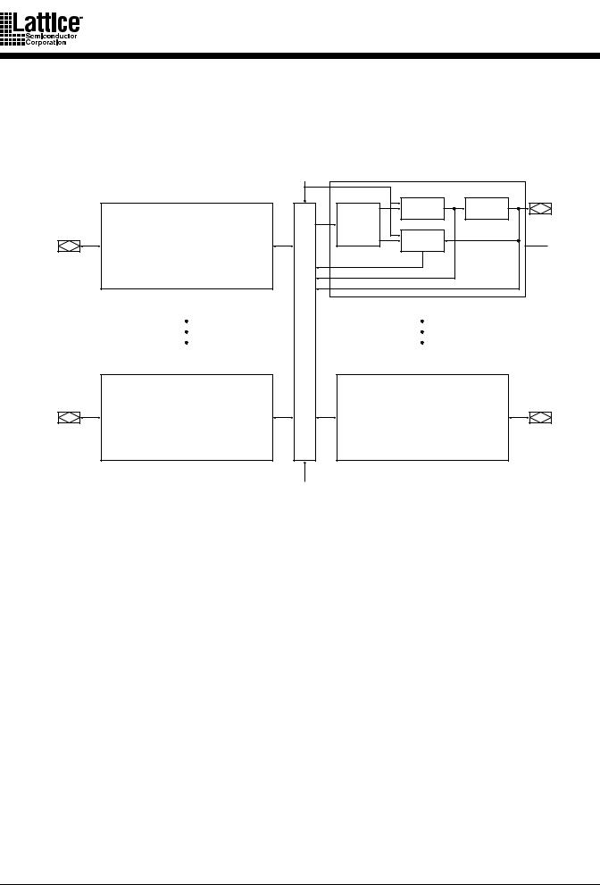
Each MACH 1 and 2 device consists of multiple, optimized PAL® blocks interconnected by a switch matrix. The switch matrix allows communication between PAL blocks, and routes inputs to the PAL blocks. Together, the PAL blocks and switch matrix allow the logic designer to create large designs in a single device instead of using multiple devices.
I/O Pins
I/O Pins
PAL Block
PAL Block
Clock/Input Pins |
|
|
|
Output |
I/O Cells |
I/O Pins |
|
Macrocells |
|||
|
|
||
Array and |
|
|
|
Allocator |
|
|
|
Buried |
|
|
|
Macrocells |
|
PAL Block |
|
(note 1) |
|
|
|
Buried Macrocell Feedback |
|
|
|
Output Macrocell Feedback |
|
|
|
I/O Pin Feedback |
|
|
|
Switch Matrix |
|
|
|
PAL Block |
|
I/O Pins |
14051K-002
Note: |
|
Dedicated Input |
|
|
|
|
|
|
|
||
1. There are no buried macrocells in MACH 1 devices. All macrocells are output macrocells. |
|
||||
|
Device |
PAL Blocks |
Macrocells per Block |
I/Os per Block |
Product Terms per Block |
|
|
|
|
|
|
|
MACH111(SP) |
2 |
16 |
16 |
70 |
|
MACH131(SP) |
4 |
16 |
16 |
70 |
|
MACH211(SP) |
4 |
16 |
8 |
68 |
|
MACH221(SP) |
8 |
12 |
6 |
52 |
|
MACH231(SP) |
8 |
16 |
8 |
68 |
Figure 1. Overall Architecture of MACH 1 & 2 Devices
The switch matrix takes all dedicated inputs and signals from the input switch matrices and routes them as needed to the PAL blocks. Feedback signals that return to the same PAL block still must go through the switch matrix. This mechanism ensures that PAL blocks in MACH devices communicate with each other with guaranteed fixed timing (SpeedLocking).
The switch matrix makes a MACH device more advanced than simply several PAL devices on a single chip. It allows the designer to think of the device not as a collection of blocks, but as a single programmable device; the software partitions the design into PAL blocks through the central switch matrix so that the designer does not have to be concerned with the internal architecture of the device.
4 |
MACH 1 & 2 Families |

Each PAL block consists of the following elements:
Product-term array
Logic Allocator
Macrocells
I/O cells
Each PAL block additionally contains an asynchronous reset product term and an asynchronous preset product term. This allows the flip-flops within a single PAL block to be initialized as a bank. There are also output enable product terms that provide tri-state control for the I/O cells.
Product-Term Array
The product-term array consists of a number of product terms that form the basis of the logic being implemented. The inputs to the AND gates come from the switch matrix (Table 4), and are provided in both true and complement forms for efficient logic implementation.
Because the number of product terms available for a given function is not fixed, the full sum of products is not realized in the array. The product terms drive the logic allocator, which allocates the appropriate number of product terms to generate the function.
Table 4. PAL Block Inputs
Device |
Number of Inputs to PAL Block |
Device |
Number of Inputs to PAL Block |
|
|
|
|
MACH111 |
26 |
MACH211SP |
26 |
|
|
|
|
MACH111SP |
26 |
MACH221 |
26 |
|
|
|
|
MACH131 |
26 |
MACH221SP |
26 |
|
|
|
|
MACH131SP |
26 |
MACH231 |
32 |
|
|
|
|
MACH211 |
26 |
MACH231SP |
32 |
|
|
|
|
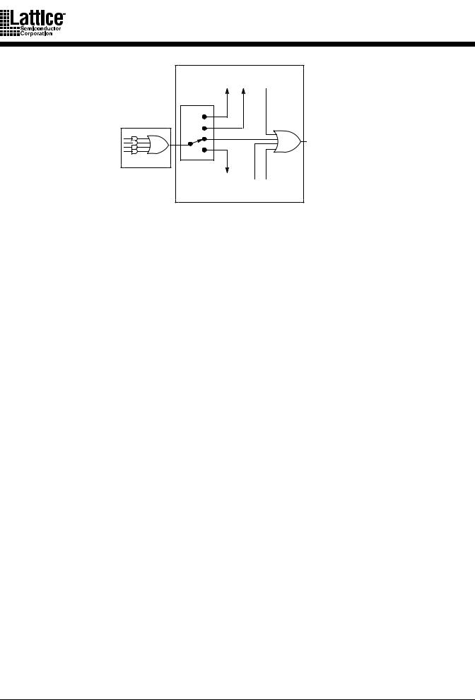
Logic Allocator
The logic allocator (Figure 2) is a block within which different product terms are allocated to the appropriate macrocells in groups of four product terms called “product term clusters”. The availability and distribution of product term clusters is automatically considered by the software as it fits functions within the PAL block. The size of the product term clusters has been designed to provide high utilization of product terms. Complex functions using many product terms are possible, and when few product terms are used, there will be a minimal number of unused, or wasted, product terms left over.
The product term clusters do not “wrap” around the logic block. This means that the macrocells at the ends of the block have fewer product terms available (Tables 5, 6, 7, 8).
MACH 1 & 2 Families |
5 |
|
To |
To |
From |
|
|
n-2 |
n-1 |
n-1 |
|
|
* |
|
|
|
n |
|
|
n |
To Macrocell |
|
|
n |
||
|
|
|
||
Product Term |
To |
|
* |
|
Cluster |
n+1 |
From |
From |
|
|
|
n+1 |
n+2 |
|
|
Logic |
|
14051K-003 |
|
|
Allocator |
*MACH 2 only |
||
Figure 2. Product Term Clusters and the Logic Allocator
Table 5. Logic Allocation for MACH111(SP)
Output Macrocell |
Available Clusters |
Output Macrocell |
Available Clusters |
|
|
|
|
M0 |
C0, C1 |
M8 |
C8, C9 |
M1 |
C0, C1, C2 |
M9 |
C8, C9, C10 |
M2 |
C1, C2, C3 |
M10 |
C9, C10, C11 |
M3 |
C2, C3, C4 |
M11 |
C10, C11, C12 |
M4 |
C3, C4, C5 |
M12 |
C11, C12, C13 |
M5 |
C4, C5, C6 |
M13 |
C12, C13, C14 |
M6 |
C5, C6, C7 |
M14 |
C13, C14, C15 |
M7 |
C6, C7 |
M15 |
C14, C15 |
Table 6. Logic Allocation for MACH131(SP)
Output Macrocell |
Available Clusters |
Output Macrocell |
Available Clusters |
|
|
|
|
M0 |
C0, C1 |
M8 |
C7, C8, C9 |
M1 |
C0, C1, C2 |
M9 |
C8, C9, C10 |
M2 |
C1, C2, C3 |
M10 |
C9, C10, C11 |
M3 |
C2, C3, C4 |
M11 |
C10, C11, C12 |
M4 |
C3, C4, C5 |
M12 |
C11, C12, C13 |
M5 |
C4, C5, C6 |
M13 |
C12, C13, C14 |
M6 |
C5, C6, C7 |
M14 |
C13, C14, C15 |
M7 |
C6, C7, C8 |
M15 |
C14, C15 |
6 |
MACH 1 & 2 Families |

Table 7. Logic Allocation for MACH211(SP) and MACH231(SP)
Macrocell |
|
Macrocell |
|
||
|
|
|
|
|
|
Output |
Buried |
Available Clusters |
Output |
Buried |
Available Clusters |
|
|
|
|
|
|
M0 |
|
C0, C1, C2 |
M8 |
|
C7, C8, C9, C10 |
|
M1 |
C0, C1, C2, C3 |
|
M9 |
C8, C9, C10, C11 |
M2 |
|
C1, C2, C3, C4 |
M10 |
|
C9, C10, C11, C12 |
|
M3 |
C2, C3, C4, C5 |
|
M11 |
C10, C11, C12, C13 |
M4 |
|
C3, C4, C5, C6 |
M12 |
|
C11, C12, C13, C14 |
|
M5 |
C4, C5, C6, C7 |
|
M13 |
C12, C13, C14, C15 |
M6 |
|
C5, C6, C7, C8 |
M14 |
|
C13, C14, C15 |
|
M7 |
C6, C7, C8, C9 |
|
M15 |
C14, C15 |
Table 8. Logic Allocation for MACH221(SP)
Macrocell |
|
Macrocell |
|
||
|
|
|
|
|
|
Output |
Buried |
Available Clusters |
Output |
Buried |
Available Clusters |
|
|
|
|
|
|
M0 |
|
C0, C1, C2 |
M6 |
|
C5, C6, C7, C8 |
|
M1 |
C0, C1, C2, C3 |
|
M7 |
C6, C7, C8, C9 |
M2 |
|
C1, C2, C3, C4 |
M8 |
|
C7, C8, C9, C10 |
|
M3 |
C2, C3, C4, C5 |
|
M9 |
C8, C9, C10, C11 |
M4 |
|
C3, C4, C5, C6 |
M10 |
|
C9, C10, C11 |
|
M5 |
C4, C5, C6, C7 |
|
M11 |
C10, C11 |
Macrocell
There are two fundamental types of macrocell: the output macrocell and the buried macrocell. The buried macrocell is only found in MACH 2 devices. The use of buried macrocells effectively doubles the number of macrocells available without increasing the pin count.
Both macrocell types can generate registered or combinatorial outputs. For the MACH 2 series, a transparent-low latch configuration is provided. If the register is used, it can be configured as a T-type or a D-type flip-flop. Register and latch functionality is defined in Table 9.
Programmable polarity (for output macrocells) and the T-type flip-flop both give the software a way to minimize the number of product terms needed. These choices can be made automatically by the software when it fits the design into the device.
Table 9. Register/Latch Operation
Configuration |
D/T |
CLK/LE |
Q+ |
||
|
|
|
|
|
|
|
X |
0,1,↓ |
|
Q |
|
|
|
|
|
|
|
D-Register |
0 |
↑ |
0 |
|
|
|
|
|
|
|
|
|
1 |
↑ |
1 |
|
|
|
|
|
|
|
|
|
X |
0,1,↓ |
|
Q |
|
|
|
|
|
|
|
T-Register |
0 |
↑ |
|
Q |
|
|
|
|
|
|
|
|
1 |
↑ |
|
|
|
|
|
Q |
|
||
|
|
|
|
|
|
|
X |
1 |
|
Q |
|
|
|
|
|
|
|
Latch |
0 |
0 |
0 |
|
|
|
|
|
|
|
|
|
1 |
0 |
1 |
|
|
|
|
|
|
|
|
MACH 1 & 2 Families |
7 |
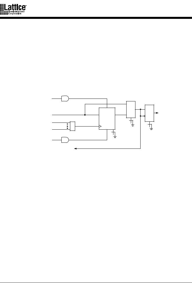
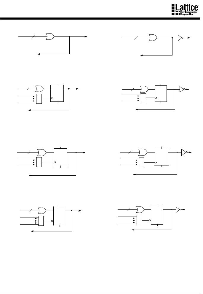
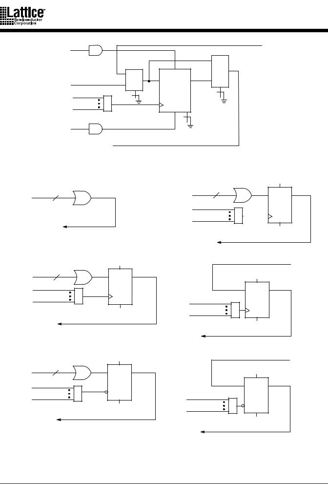
The output macrocell (Figure 3) sends its output back to the switch matrix, via internal feedback, and to the I/O cell. The feedback is always available regardless of the configuration of the I/O cell. This allows for buried combinatorial or registered functions, freeing up the I/O pins for use as inputs if not needed as outputs. The basic output macrocell configurations are shown in Figure 4.
The buried macrocell (Figure 5) does not send its output to an I/O cell. The output of a buried macrocell is provided only as an internal feedback signal which feeds the switch matrix. This allows the designer to generate additional logic without requiring additional pins. The buried macrocell can also be used to register or latch inputs. The input register is a D-type flip-flop; the input latch is a transparent-low D-type latch. Once configured as a registered or latched input, the buried macrocell cannot generate logic from the product-term array. The basic buried macrocell configurations are shown in Figure 6.
PAL-Block |
|
|
|
|
|
Asynchronous |
|
|
|
|
|
Preset |
|
|
1 |
|
|
|
|
|
|
|
|
Sum of Products |
|
AP |
|
1 |
To I/O |
from Logic |
|
D/T/L1 Q |
0 |
|
|
|
0 |
Cell |
|||
Allocator |
|
|
|
|
|
|
|
|
|
|
|
CLK0 |
|
AR |
|
|
|
CLKn |
|
|
|
|
|
|
|
|
|
|
|
PAL-Block |
|
|
|
|
|
Asynchronous |
|
|
|
|
|
Reset |
To |
|
|
|
|
|
Switch |
|
|
|
|
|
Matrix |
|
|
|
14051K-004 |
Note:
1. Latch option available on MACH 2 devices only.
Figure 3. Output Macrocell
8 |
MACH 1 & 2 Families |
From |
n |
|
To |
From |
n |
|
To |
Logic |
|
I/O |
|
||||
|
|
Cell |
Logic |
|
|
I/O |
|
Allocator |
|
|
|
|
|||
|
|
|
Allocator |
|
|
Cell |
|
|
|
|
|
|
|
|
|
|
To Switch |
|
|
|
To Switch |
|
|
|
Matrix |
|
|
|
|
|
|
|
|
|
|
Matrix |
|
|
|
|
|
|
|
|
|
|
|
|
a. Combinatorial, active high |
|
|
|
b. Combinatorial, active low |
|
|
From |
n |
To |
|
From |
|
|
To |
Logic |
|
Logic |
n |
|
|||
Allocator |
D APQ |
I/O |
|
Allocator |
D APQ |
I/O |
|
|
|
||||||
CLK0 |
|
Cell |
|
CLK0 |
|
|
Cell |
AR |
|
|
|
AR |
|
||
CLKn |
|
|
CLKn |
|
|
||
|
|
|
|
|
|
||
To Switch |
|
|
To Switch |
|
|
||
Matrix |
|
|
|
Matrix |
|
|
|
|
c. D-type register, active high |
|
|
|
d. D-type register, active low |
|
|
From |
|
|
|
|
Logic |
n |
T APQ |
To |
|
Allocator |
I/O |
|||
CLK0 |
|
|
Cell |
|
|
|
|
||
CLKn |
|
AR |
|
|
To Switch |
|
|
|
|
Matrix |
|
|
|
|
e. T-type register, active high |
|
|||
From |
|
|
To |
|
Logic |
n |
L APQ |
||
I/O |
||||
Allocator |
||||
|
|
Cell |
||
CLK0 |
|
|
||
|
G AR |
|
||
CLK |
|
|
||
n |
|
|
|
|
To Switch |
|
|
|
|
Matrix |
|
|
|
|
g. Latch, active high (MACH 2 only)
From |
|
|
|
Logic |
n |
T AP Q |
To |
Allocator |
I/O |
||
CLK0 |
|
|
Cell |
|
AR |
|
|
CLKn |
|
|
|
|
|
|
|
To Switch |
|
|
|
|
Matrix |
|
|
|
f. T-type register, active low |
|
|
From |
|
|
|
Logic |
n |
L APQ |
To |
Allocator |
|
||
CLK0 |
|
|
I/O |
|
G AR |
Cell |
|
CLKn |
|
|
|
To Switch 
Matrix
h. Latch, active low (MACH 2 only)
14051K-005
Figure 4. Output Macrocell Configurations
MACH 1 & 2 Families |
9 |
PAL-Block |
|
|
From I/O Pin |
|
Asynchronous |
|
|
|
|
Preset |
|
|
1 |
|
|
|
|
||
Sum of Products |
1 |
AP |
|
|
D/T/L Q |
0 |
|||
From Logic |
0 |
|||
|
|
|||
IC Allocator |
|
|
|
|
CLK0 |
|
|
|
|
CLKn |
|
AR |
|
PAL-Block
Asynchronous
Reset To
Switch 14051K-030
Matrix
Figure 5. Buried Macrocell (MACH 2 only)
From |
n |
|
Logic |
|
|
|
|
|
Allocator |
|
|
|
To Switch |
|
|
Matrix |
|
|
a. Combinatorial |
|
From Logic |
n |
AP |
Allocator |
T |
Q |
|
|
|
CLK0 |
|
|
CLKn |
|
AR |
To Switch
Matrix
|
c. T-type register |
|
|
From |
n |
L |
AP |
Logic |
|
Q |
|
Allocator |
|
|
|
CLK0 |
|
G |
|
CLKn |
|
AR |
|
|
|
To Switch
Matrix
e. Latch
From Logic |
n |
AP |
Allocator |
|
D Q |
CLKÂ0 |
|
|
CLÂKn |
|
AR |
|
|
To Switch
Matrix
b. D-type register
From I/O
Cell
AP
D Q
CLK0
CLKn |
AR |
To Switch
Matrix
d. Input register
From I/O
Cell
AP
L Q
CLK0
CLKn |
G |
AR |
To Switch
Matrix
f. Input latch
14051K-006
Figure 6. Buried Macrocell Configurations (MACH 2 only)
10 |
MACH 1 & 2 Families |
The flip-flops in either macrocell type can be clocked by one of several clock pins (Table 10). Registers are clocked on the rising edge of the clock input. Latches hold their data when the gate input is HIGH. Clock pins are also available as inputs, although care must be taken when a signal acts as both clock and input to the same device.
Table 10. Macrocell Clocks
Device |
Number of Clocks Available |
Device |
Number of Clocks Available |
|
|
|
|
MACH111 |
4 |
MACH211SP |
2 |
|
|
|
|
MACH111SP |
2 |
MACH221 |
4 |
|
|
|
|
MACH131 |
4 |
MACH221SP |
4 |
|
|
|
|
MACH131SP |
4 |
MACH231 |
4 |
|
|
|
|
MACH211 |
4 |
MACH231SP |
4 |
|
|
|
|
All flip-flops have asynchronous reset and preset. This is controlled by the common product terms that control all flip-flops within a PAL block. For a single PAL block, all flip-flops, whether in an output or a buried macrocell, are initialized together. The initialization functionality of the flip-flops is illustrated in Table 11.
Table 11. Asynchronous Reset/Preset Operation
Configuration |
AR |
AP |
CLK/LE |
Q+ |
|
|
|
|
|
|
|
|
0 |
0 |
X |
See Table 9 |
|
|
|
|
|
|
|
Register |
0 |
1 |
X |
1 |
|
|
|
|
|
||
1 |
0 |
X |
0 |
||
|
|||||
|
|
|
|
|
|
|
1 |
1 |
X |
0 |
|
|
|
|
|
|
|
|
0 |
0 |
X |
See Table 9 |
|
|
|
|
|
|
|
|
0 |
1 |
0 |
Illegal |
|
|
|
|
|
|
|
|
0 |
1 |
1 |
1 |
|
Latch |
|
|
|
|
|
1 |
0 |
0 |
Illegal |
||
|
|
|
|
|
|
|
1 |
0 |
1 |
0 |
|
|
|
|
|
|
|
|
1 |
1 |
0 |
Illegal |
|
|
|
|
|
|
|
|
1 |
1 |
1 |
0 |
|
|
|
|
|
|
I/O Cells
The I/O cells (Figure 7) provide a three-state output buffer. The three-state buffer can be left permanently enabled for use only as an output, permanently disabled for use as an input, or it can be controlled by one of two product terms for bi-directional signals and bus connections. The two product terms provided are common to a bank of I/O cells.
MACH 1 & 2 Families |
11 |
Output Enable |
|
|
0 1 |
|
|
|
||||||||||
Product Terms |
|
|
1 1 |
|
|
|
||||||||||
(Common to bank of |
|
|
|
|
|
|||||||||||
|
|
|
|
|
|
|
|
|
|
|
|
|
|
|
|
|
I/O Cells) |
VCC |
1 0 |
|
|
|
|||||||||||
|
|
|
0 0 |
|
|
|
||||||||||
|
|
|
|
|
|
|
|
|
|
|
|
|
|
|
|
|
|
From Output |
|
|
|
|
|
|
|
|
|
|
|
|
|
|
|
|
|
|
|
|
|
|
|
|
|
|
|
|
|
|
||
|
|
|
|
|
|
|
|
|
|
|
|
|
|
|
||
|
Macrocell |
|
|
|
|
|
|
|
|
|
|
|
|
|
|
|
|
To Switch |
|
|
|
|
|
|
|
|
|
|
|
|
|
|
|
|
Matrix |
|
|
|
|
|
|
|
|
|
|
|
|
|
|
|
|
|
|
|
|
|
|
|
|
|
|
|
|
|
|
|
|
|
|
|
|
|
|
|
|
|
|
|
|
|
|
|
|
|
To Buried |
|
Macrocell |
14051K-007 |
(MACH 2 only) |
Figure 7. I/O Cell
SPEEDLOCKING FOR GUARANTEED FIXED TIMING
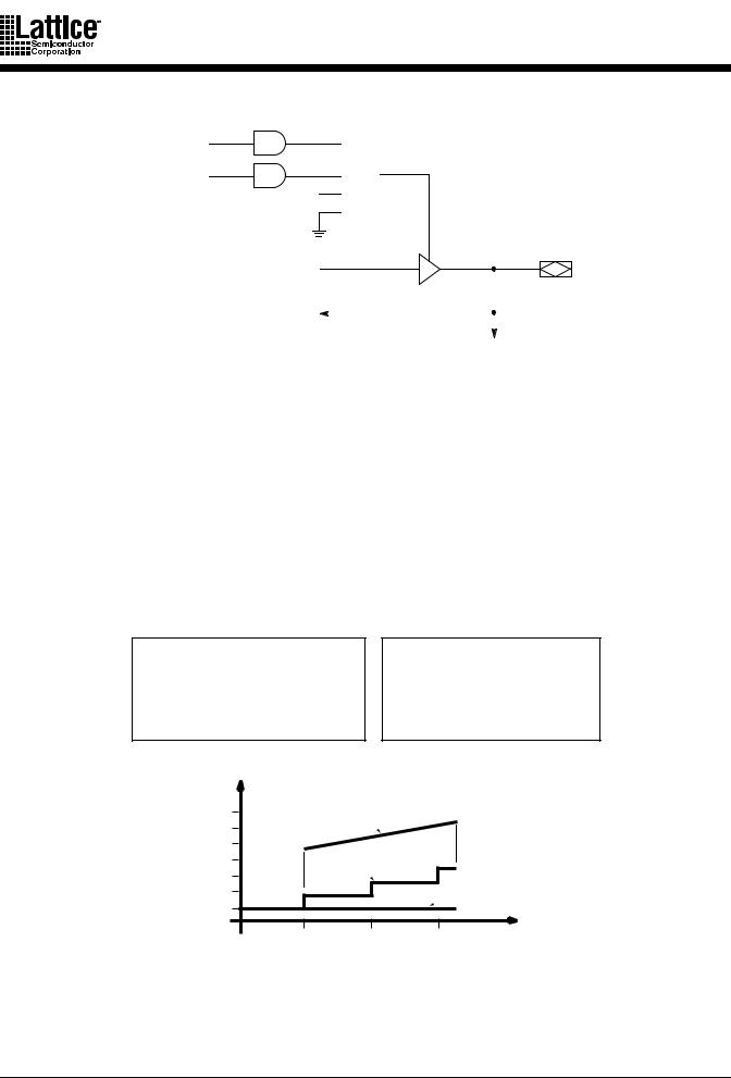
The unique MACH 1 & 2 architecture is designed for high performance—a metric that is met in both raw speed, and even more importantly, guaranteed fixed speed. The design of the switch matrix and PAL blocks guarantee a fixed pin-to-pin delay that is independent of the logic required by the design. Other non-Lattice/Vantis CPLDs incur serious timing delays as product terms expand beyond their typical 4 or 5 product term limits (Figure 8). Speed and SpeedLocking combine to give designers easy access to the performance required in today’s designs.
MACH 1 & 2 SpeedLocking
•Patented Architecture
•Path Independent
•Logic/Routing Independent
•Guaranteed Fixed Timing
•Up to 16 Product Terms per Output
Non-MACH
•Variable
•Path Dependent
•Logic/Routing Dependent Delays
•Unpredictable
•4-5 Product Terms before Delays
|
|
|
SpeedLocking |
|
||
|
11 |
Shared Expander Delay |
|
10.4 ns |
||
|
|
|
|
|||
|
10 |
8.8 ns |
|
|
Non-MACH |
|
tPD (ns) |
9 |
|
|
|||
Parallel Expander Delay |
7.4 ns |
|||||
|
8 |
|||||
|
7 |
|
6.6 ns |
|
|
|
|
6 |
5.8 ns |
|
MACH 1 & 2 |
||
|
5 ns |
|
|
|||
|
5 |
|
|
|||
|
|
|
|
|
||
|
|
5 PT |
10 PT |
15 PT |
||
|
|
|
Product Terms |
14051K-001 |
||
|
|
|
|
|||
Figure 8. Timing in MACH 1 & 2 vs. Non-MACH Devices
12 |
MACH 1 & 2 Families |

JTAG IN-SYSTEM PROGRAMMING
Programming devices in-system provides a number of significant benefits including: rapid prototyping, lower inventory levels, higher quality, and the ability to make in-field modifications. All MACHxxxSP devices provide in-system programming (ISP) capability through their JTAG ports. This capability has been implemented in a manner that insures that the JTAG port remains compliant to the IEEE 1149.1 standard. By using JTAG as the communication interface through which ISP is achieved, customers benefit from a standard, well-defined interface.
MACHxxxSP devices can be programmed across the commercial temperature and voltage range. These devices tristate the outputs during programming. Lattice/Vantis provides its free PC-based Lattice/VantisPRO software to facilitate in-system programming. Lattice/VantisPRO software takes the JEDEC file output produced by Vantis’ design implementation software, along with information about the JTAG chain, and creates a set of vectors that are used to drive the JTAG chain. Lattice/ VantisPRO software can use these vectors to drive a JTAG chain via the parallel port of a PC.
Alternatively, Lattice/VantisPRO software can output files in formats understood by common automated test equipment. This equipment can then be used to program MACHxxxSP devices during the testing of a circuit board. For more information about in-system programming, refer to the separate document entitled MACH ISP Manual.
BUS-FRIENDLY INPUTS AND I/Os
The MACH 1 & 2 inputs and I/Os include two inverters in series which loop back to the input. This double inversion weakly holds the input at its last driven logic state. For the circuit diagram, please refer to the Input/Output Equivalent Schematics (page 393) in the General Information Section of the Vantis 1999 Data Book.
PCI COMPLIANT
The MACH 1 & 2 families in -5/-6/-7/-10/-12 speed grades are fully compliant with the PCI Local Bus Specification published by the PCI Special Interest Group. The MACH 1 & 2 families’ predictable timing ensures compliance with the PCI AC specifications independent of the design.
POWER-DOWN MODE
The MACH 1 & 2 families feature a programmable low-power mode in which individual signal paths can be programmed for low power. These low-power speed paths will be slower than the non-low-power paths. This feature allows speed critical paths to run at maximum frequency while the rest of the paths operate in the low-power mode, resulting in power savings of up to 75%. If all of the signals in a PAL block are in low-power mode, then the total power is reduced even further.
SAFE FOR MIXED SUPPLY VOLTAGE SYSTEM DESIGNS
All MACHxxxSP and most of the MACH 1 & 2 devices are safe for mixed supply voltage system designs. These 5-V devices will not overdrive 3.3-V devices above the output voltage of 3.3 V, while they can accept inputs from other 3.3-V devices. The MACH 1 & 2 families provide easy-to- use mixed-voltage design compatibility. For more information, refer to the Technical Note entitled
Mixed Supply Design with MACH 1 & 2 SP Devices.
POWER-UP RESET
All flip-flops power-up to a logic LOW for predictable system initialization. The actual values of the outputs of the MACH devices will depend on the configuration of the macrocell. To guarantee
MACH 1 & 2 Families |
13 |

initialization values, the VCC rise must be monotonic and the clock must be inactive until the reset delay time has elapsed.
SECURITY BIT
A security bit is provided on the MACH devices as a deterrent to unauthorized copying of the array configuration patterns. Once programmed, this bit defeats readback of the programmed pattern by a device programmer, securing proprietary designs from competitors. Programming and verification are also defeated by the security bit. The bit can only be reset by erasing the entire device.
14 |
MACH 1 & 2 Families |

MACH111(SP) AND MACH131(SP) PAL BLOCK
0 |
4 |
8 |
12 |
16 |
20 |
24 |
28 |
32 |
36 |
40 |
43 |
47 |
51 |
Output Enable
Output Enable
Asynchronous Reset
Asynchronous Preset
|
|
|
|
|
|
|
|
|
|
|
|
|
|
|
|
|
|
|
I/O |
I/O |
|
|
|
|
|
|
|
|
|
|
|
|
|
|
|
|
M0 |
Output |
Cell |
||
|
|
|
|
|
|
|
|
|
|
|
|
|
|
|
|
|
|
|||
|
|
|
|
|
|
|
|
|
|
|
|
|
|
|
|
Macro |
|
|
||
|
|
|
|
|
|
|
|
|
|
|
|
|
|
|
|
Cell |
|
|
||
|
|
|
|
|
|
|
|
|
|
|
|
|
|
|
|
|
|
|
I/O |
|
|
|
|
|
|
|
|
|
|
|
|
|
|
|
|
|
|
|
Output |
Cell |
I/O |
|
|
|
|
|
|
|
|
|
|
|
|
|
|
|
|
M1 |
|
|
||
|
|
|
|
|
|
|
|
|
|
|
|
|
|
|
|
Macro |
|
|
||
|
|
|
|
|
|
|
|
|
|
|
|
|
|
|
|
Cell |
|
|
||
|
|
|
|
|
|
|
|
|
|
|
|
|
|
|
|
|
|
|
I/O |
I/O |
|
|
|
|
|
|
|
|
|
|
|
|
|
|
|
|
M2 |
Output |
Cell |
||
|
|
|
|
|
|
|
|
|
|
|
|
|
|
|
|
|
||||
|
|
|
|
|
|
|
|
|
|
|
|
|
|
|
|
|
|
|||
|
|
|
|
|
|
|
|
|
|
|
|
|
|
|
|
Macro |
|
|
||
|
|
|
|
|
|
|
|
|
|
|
|
|
|
|
|
|
|
Cell |
|
|
|
|
|
|
|
|
|
|
|
|
|
|
|
|
|
|
|
|
|
I/O |
|
|
|
|
|
|
|
|
|
|
|
|
|
|
|
|
|
|
|
Output |
Cell |
I/O |
|
|
|
|
|
|
|
|
|
|
|
|
|
|
|
|
M3 |
|
|
||
|
|
|
|
|
|
|
|
|
|
|
|
|
|
|
|
Macro |
|
|
||
|
|
|
|
|
|
|
|
|
|
|
|
|
|
|
|
Cell |
|
|
||
0 |
|
|
|
|
|
|
|
|
|
|
|
|
|
|
|
|
|
|
I/O |
|
|
|
|
|
|
|
|
|
|
|
|
|
|
|
|
|
|
|
|
|
|
|
|
|
|
|
|
|
|
|
|
|
|
|
C0 |
|
M4 |
Output |
Cell |
I/O |
||
|
|
|
|
|
|
|
|
|
|
|
|
|
|
|
|
|||||
|
|
|
|
|
|
|
|
|
|
|
|
|
|
|
|
Macro |
|
|
||
|
|
|
|
|
|
|
|
|
|
|
|
|
C1 |
|
Cell |
|
|
|||
|
|
|
|
|
|
|
|
|
|
|
|
|
|
|
|
|
|
|
||
|
|
|
|
|
|
|
|
|
|
|
|
|
C2 |
|
|
|
|
I/O |
I/O |
|
|
|
|
|
|
|
|
|
|
|
|
|
|
|
|
|
Output |
Cell |
|||
|
|
|
|
|
|
|
|
|
|
|
|
|
|
M5 |
|
|
||||
|
|
|
|
|
|
|
|
|
|
|
|
|
|
|
|
Macro |
|
|
||
|
|
|
|
|
|
|
|
|
|
|
|
|
C3 |
|
Cell |
|
|
|||
|
|
|
|
|
|
|
|
|
|
|
|
|
|
|
|
|
|
|
||
|
|
|
|
|
|
|
|
|
|
|
|
|
C4 |
|
|
|
|
I/O |
I/O |
|
|
|
|
|
|
|
|
|
|
|
|
|
|
|
|
|
Output |
Cell |
|||
|
|
|
|
|
|
|
|
|
|
|
|
|
|
M6 |
|
|
||||
|
|
|
|
|
|
|
|
|
|
|
|
|
|
|
Allocator |
Macro |
|
|
||
|
|
|
|
|
|
|
|
|
|
|
|
|
C5 |
Cell |
|
|
||||
|
|
|
|
|
|
|
|
|
|
|
|
|
|
|
|
|||||
|
|
|
|
|
|
|
|
|
|
|
|
|
|
|
|
|
|
|
||
|
|
|
|
|
|
|
|
|
|
|
|
|
C |
|
|
|
|
|
I/O |
I/O |
Switch |
|
|
|
|
|
|
|
|
|
|
|
|
6 |
|
|
|
Macro |
Cell |
||
|
|
|
|
|
|
|
|
|
|
|
|
|
|
|
M7 |
Output |
|
|
||
Matrix |
|
|
|
|
|
|
|
|
|
|
|
|
C7 |
Logic |
Cell |
|
|
|||
|
|
|
|
|
|
|
|
|
|
|
|
|
|
|
|
|
|
|||
|
|
|
|
|
|
|
|
|
|
|
|
|
C8 |
|
|
Output |
I/O |
I/O |
||
|
|
|
|
|
|
|
|
|
|
|
|
|
|
|
|
|
|
|
Cell |
|
|
|
|
|
|
|
|
|
|
|
|
|
|
|
|
|
M8 |
Macro |
|
|
|
|
|
|
|
|
|
|
|
|
|
|
|
|
C9 |
|
Cell |
|
|
|||
|
|
|
|
|
|
|
|
|
|
|
|
|
|
|
|
|
|
|
||
|
|
|
|
|
|
|
|
|
|
|
|
|
C10 |
|
|
|
|
I/O |
|
|
|
|
|
|
|
|
|
|
|
|
|
|
|
|
|
|
Output |
Cell |
I/O |
||
|
|
|
|
|
|
|
|
|
|
|
|
|
|
|
|
|
|
|||
|
|
|
|
|
|
|
|
|
|
|
|
|
|
|
|
M9 |
Macro |
|
|
|
|
|
|
|
|
|
|
|
|
|
|
|
|
C11 |
|
Cell |
|
|
|||
|
|
|
|
|
|
|
|
|
|
|
|
|
|
|
|
|
|
|||
|
|
|
|
|
|
|
|
|
|
|
|
|
|
|
|
|
|
|
||
|
|
|
|
|
|
|
|
|
|
|
|
|
C12 |
|
|
|
|
I/O |
I/O |
|
|
|
|
|
|
|
|
|
|
|
|
|
|
|
|
|
Output |
Cell |
|||
|
|
|
|
|
|
|
|
|
|
|
|
|
C |
|
|
M10 |
Macro |
|
|
|
|
|
|
|
|
|
|
|
|
|
|
|
|
13 |
|
Cell |
|
|
|||
|
|
|
|
|
|
|
|
|
|
|
|
|
|
|
|
|
||||
|
|
|
|
|
|
|
|
|
|
|
|
|
|
|
|
|
|
|
|
|
|
|
|
|
|
|
|
|
|
|
|
|
|
C14 |
|
|
|
|
I/O |
I/O |
|
|
|
|
|
|
|
|
|
|
|
|
|
|
|
|
|
Output |
Cell |
|||
|
|
|
|
|
|
|
|
|
|
|
|
|
C15 |
|
|
|
Macro |
|
|
|
|
|
|
|
|
|
|
|
|
|
|
|
|
|
M |
|
Cell |
|
|
||
|
|
|
|
|
|
|
|
|
|
|
|
|
|
11 |
|
|
|
|||
63 |
|
|
|
|
|
|
|
|
|
|
|
|
|
|
|
|
|
|
|
|
|
|
|
|
|
|
|
|
|
|
|
|
|
|
|
|
|
|
|
|
|
|
|
|
|
|
|
|
|
|
|
|
|
|
|
|
|
|
|
|
I/O |
I/O |
|
|
|
|
|
|
|
|
|
|
|
|
|
|
|
|
|
|
Output |
Cell |
|
|
|
|
|
|
|
|
|
|
|
|
|
|
|
|
|
|
|
|
|
|
|
|
|
|
|
|
|
|
|
|
|
|
|
|
|
|
|
|
Macro |
|
|
|
|
|
|
|
|
|
|
|
|
|
|
|
|
|
|
M12 |
Cell |
|
|
|
|
|
|
|
|
|
|
|
|
|
|
|
|
|
|
|
|
|
|
||
|
|
|
|
|
|
|
|
|
|
|
|
|
|
|
|
|
|
|
I/O |
|
|
|
|
|
|
|
|
|
|
|
|
|
|
|
|
|
|
|
Output |
Cell |
I/O |
|
|
|
|
|
|
|
|
|
|
|
|
|
|
|
|
|
|
|
|
|
|
|
|
|
|
|
|
|
|
|
|
|
|
|
|
|
M13 |
Macro |
|
|
|
|
|
|
|
|
|
|
|
|
|
|
|
|
|
|
|
Cell |
|
|
||
|
|
|
|
|
|
|
|
|
|
|
|
|
|
|
|
|
|
|
||
|
|
|
|
|
|
|
|
|
|
|
|
|
|
|
|
|
|
|
I/O |
|
|
|
|
|
|
|
|
|
|
|
|
|
|
|
|
|
|
|
|
Cell |
I/O |
|
|
|
|
|
|
|
|
|
|
|
|
|
|
|
|
|
|
Output |
|
|
|
|
|
|
|
|
|
|
|
|
|
|
|
|
|
|
M14 |
Macro |
|
|
|
|
|
|
|
|
|
|
|
|
|
|
|
|
|
|
|
Cell |
|
|
||
|
|
|
|
|
|
|
|
|
|
|
|
|
|
|
|
|
|
|
||
|
|
|
|
|
|
|
|
|
|
|
|
|
|
|
|
|
|
|
I/O |
|
|
|
|
|
|
|
|
|
|
|
|
|
|
|
|
|
|
|
|
Cell |
I/O |
|
|
|
|
|
|
|
|
|
|
|
|
|
|
|
|
|
|
Output |
|
|
|
|
|
|
|
|
|
|
|
|
|
|
|
|
|
|
M15 |
Macro |
|
|
|
|
|
|
|
|
|
|
|
|
|
|
|
|
|
|
|
Cell |
|
|
||
|
|
|
|
|
|
|
|
|
|
|
|
|
|
|
|
|
|
|
|
|
|
|
|
|
|
|
|
|
|
|
|
|
|
|
|
|
|
|
CLK |
|
|
|
|
|
|
|
|
|
|
|
|
|
|
|
|
|
for MACH111SP |
2 |
|
|
||
|
|
|
|
|
|
|
|
|
|
|
|
|
|
|
|
|
|
|
|
|
|
|
|
|
|
|
|
|
|
|
|
|
|
for MACH111, MACH131, MACH131SP |
4 |
|
|
||||
|
|
|
|
|
|
|
|
|
|
|
|
|
|
|
|
|
|
|
|
|
|
|
|
|
|
|
|
|
|
|
|
|
|
Output Enable |
|
|
|
|
|
|
|
|
|
|
|
|
|
|
|
|
|
|
|
|
Output Enable |
|
|
|
|
|
|
|
0 |
4 |
8 |
12 |
16 |
20 |
24 |
28 |
32 |
36 |
40 |
43 |
47 |
51 |
|
|
|
|
|
|
|
|
|
16 |
|
|
|
|
|
|
|
|
|
|
|
|
|
|
|
|
|
|
|
|
|
16 |
|
|
|
|
|
|
|
|
|
|
|
|
|
|
|
14051K-013 |
|
|
|
|
|
|
|
|
|
|
|
|
|
|
|
|
|
|
|
|
||
|
|
|
|
|
|
|
|
MACH 1 & 2 Families |
|
|
|
|
|
|
15 |
|||||
Loading...