

Lattice Semiconductor Corporation PALCE16V8H-10JC-4, PALCE16V8Q-15PC-4, PALCE16V8Q-20JI-4, PALCE16V8Q-20PI-4, PALCE16V8H-15SC-4 Datasheet
...
PALCE16V8
PALCE16V8Z
COM’L:H-5/7/10/15/25, Q-10/15/25 IND:H-10/15/25, Q-20/25
COM’L:-25 IND:-12/15/25
P ALCE16V8 and PALCE16V8Z Families
EE CMOS (Zero-Power) 20-Pin Universal
Programmable Array Logic
DISTINCTIVE CHARACTERISTICS
Pin and function compatible with all 20-pin PAL® devices
◆
Electrically erasable CMOS technology provides reconfigurable logic and full testability
◆
◆
High-speed CMOS technology
— 5-ns propagation delay for “-5” version
— 7.5-ns propagation delay for “-7” version
◆
Direct plug-in replacement for the PAL16R8 series
◆
Outputs programmable as registered or combinatorial in any combination
◆
Peripheral Component Interconnect (PCI) compliant
Programmable output polarity
◆
◆
Programmable enable/disable control
◆
Preloadable output registers for testability
Automatic register reset on power up
◆
Cost-effective 20-pin plastic DIP, PLCC, and SOIC packages
◆
◆
Extensive third-party software and programmer support
◆
Fully tested for 100% programming and functional yields and high reliability
5-ns version utilizes a split leadframe for improved performance
◆
GENERAL DESCRIPTION
The PALCE16V8 is an advanced PAL
erasable CMOS technology. It is functionally compatible with all 20-pin GAL devices. The
macrocells provide a universal device architecture. The PALCE16V8 will directly replace the
PAL16R8, with the exception of the PAL16C1.
The PALCE16V8Z provides zero standby power and high speed. At 30-µA maximum standby
current, the PALCE16V8Z allows battery-powered operation for an extended period.
The P ALCE16V8 utilizes the familiar sum-of-products (AND/OR) architecture that allows users to
implement complex logic functions easily and efficiently. Multiple levels of combinatorial logic
can always be reduced to sum-of-products form, taking advantage of the very wide input gates
available in PAL devices. The equations are programmed into the device through floating-gate
USE GAL DEVICES FOR
cells in the AND logic array that can be erased electrically.
The fixed OR array allows up to eight data product terms per output for logic functions. The
sum of these products feeds the output macrocell. Each macrocell can be programmed as
registered or combinatorial with an active-high or active-low output. The output configuration
is determined by two global bits and one local bit controlling four multiplexers in each
macrocell.
device built with low-power, high-speed, electrically-
NEW DESIGNS
Publication# 16493 Rev: F
Amendment/0 Issue Date: September 2000
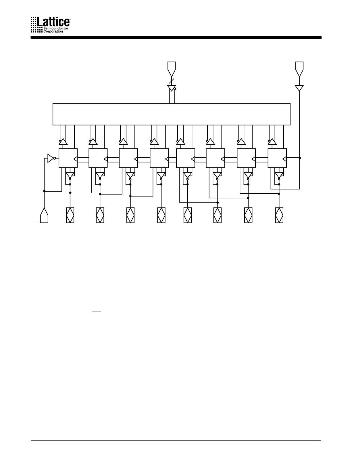
BLOCK DIAGRAM
I1 – I
8
8
CLK/I
0
OE/I
Programmable AND Array
MACRO
MC
0
9
I/O
0
MACRO
MC
1
I/O
1
MACRO
MC
2
I/O
2
MACRO
MC
3
I/O
3
32 x 64
MACRO
MC
4
I/O
4
MACRO
MC
5
I/O
5
MACRO
MC
6
I/O
6
MACRO
MC
7
I/O
7
16493E-1
FUNCTIONAL DESCRIPTION
The PALCE16V8 is a universal PAL device. The PALCE16V8Z is the zero-power version of the
PALCE16V8. It has all the architectural features of the PALCE16V8. In addition, the PALCE16V8Z
has zero standby power and an unused product term disable feature for reduced power
-
MC
consumption. It has eight independently configurable macrocells (MC
be configured as registered output, combinatorial output, combinatorial I/O or dedicated input.
The programming matrix implements a programmable AND logic array, which drives a fixed OR
logic array. Buffers for device inputs have complementary outputs to provide userprogrammable input signal polarity. Pins 1 and 11 serve either as array inputs or as clock (CLK)
and output enable (OE
USE GAL DEVICES FOR
), respectively, for all flip-flops.
NEW DESIGNS
). Each macrocell can
0
7
Unused input pins should be tied directly to V
or GND. Product terms with all bits
CC
unprogrammed (disconnected) assume the logical HIGH state, and product terms with both true
and complement of any input signal connected assume a logical LOW state.
The programmable functions on the PALCE16V8 are automatically configured from the user’s
design specification. The design specification is processed by development software to verify
the design and create a programming file (JEDEC). This file, once downloaded to a programmer,
configures the device according to the user’s desired function.
The user is given two design options with the PALCE16V8. First, it can be programmed as a
standard P AL device from the P AL16R8 series. The P AL programmer manufacturer will supply
device codes for the standard PAL device architectures to be used with the PALCE16V8.
The programmer will program the P ALCE16V8 in the corresponding architecture. This allows
the user to use existing standard PAL device JEDEC files without making any changes to them.
2 PALCE16V8 and PALCE16V8Z Families
Alternatively, the device can be programmed as a PALCE16V8. Here the user must use the
PALCE16V8 device code. This option allows full utilization of the macrocell.
To
Adjacent
Macrocell
I/O
X
1 1
0 X
1 0
SG1
SL0
OE
V
CC
X
DQ
1 1
1 0
0 0
0 1
1 1
0 X
1 0
SL1
X
*In macrocells MC0 and MC7, SG1 is replaced by SG0 on the feedback multiplexer.
Figure 1. PALCE16V8 Macrocell
CLK
Q
1 0
1 1
*SG1
0 X
SL0
X
From
Adjacent
Pin
16493E-2
CONFIGURATION OPTIONS
Each macrocell can be configured as one of the following: registered output, combinatorial
output, combinatorial I/O, or dedicated input. In the registered output configuration, the output
buffer is enabled by the OE
pin. In the combinatorial configuration, the buffer is either controlled
by a product term or always enabled. In the dedicated input configuration, it is always disabled.
With the exception of MC
and MC
0
input signal from an adjacent I/O. MC
, a macrocell configured as a dedicated input derives the
7
NEW DESIGNS
derives its input from pin 11 (OE) and MC
0
from pin 1
7
(CLK).
USE GAL DEVICES FOR
The macrocell configurations are controlled by the configuration control word. It contains 2
global bits (SG0 and SG1) and 16 local bits (SL0
through SL0
0
determines whether registers will be allowed. SG1 determines whether the PALCE16V8 will
emulate a PAL16R8 family or a PAL10H8 family device. Within each macrocell, SL0
conjunction with SG1, selects the configuration of the macrocell, and SL1
either active low or active high for the individual macrocell.
and SL1
7
through SL1
0
sets the output as
x
, in
x
7
). SG0
The configuration bits work by acting as control inputs for the multiplexers in the macrocell.
There are four multiplexers: a product term input, an enable select, an output select, and a
feedback select multiplexer. SG1 and SL0
and MC
MC
0
the adjacent pin for MC
, SG0 replaces SG1 on the feedback multiplexer. This accommodates CLK being
7
and OE the adjacent pin for MC
7
PALCE16V8 and PALCE16V8Z Families 3
are the control signals for all four multiplexers. In
x
.
0
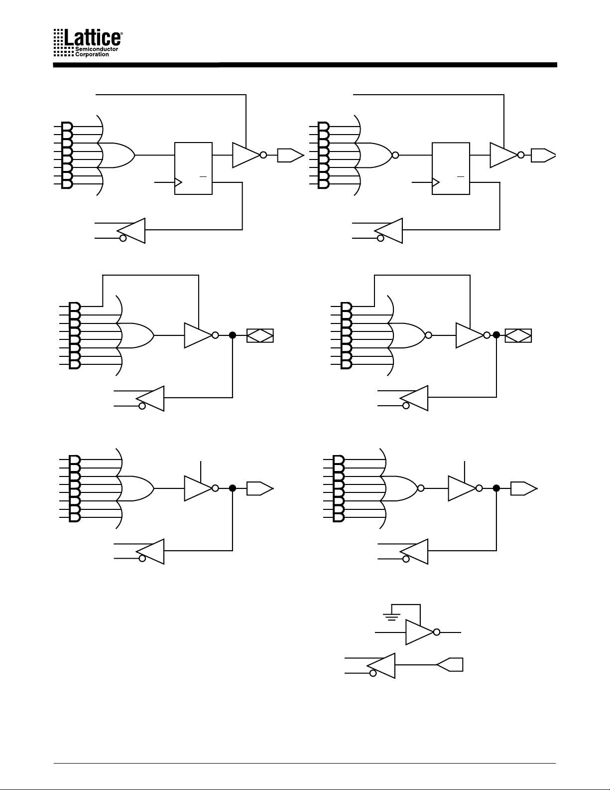
Registered Output Configuration
The control bit settings are SG0 = 0, SG1 = 1 and SL0
= 0. There is only one registered
x
configuration. All eight product terms are available as inputs to the OR gate. Data polarity is
determined by SL1
path is from Q
The flip-flop is loaded on the LOW-to-HIGH transition of CLK. The feedback
x.
on the register. The output buffer is enabled by OE.
Combinatorial Configurations
The PALCE16V8 has three combinatorial output configurations: dedicated output in a nonregistered device, I/O in a non-registered device and I/O in a registered device.
Dedicated Output in a Non-Registered Device
The control bit settings are SG0 = 1, SG1 = 0 and SL0
= 0. All eight product terms are available
x
to the OR gate. Although the macrocell is a dedicated output, the feedback is used, with the
exception of pins 15 and 16. Pins 15 and 16 do not use feedback in this mode. Because CLK
and OE
1 will use the feedback path of MC
are not used in a non-registered device, pins 1 and 11 are available as input signals. Pin
, and pin 11 will use the feedback path of MC
7
.
0
Combinatorial I/O in a Non-Registered Device
The control bit settings are SG0 = 1, SG1 = 1, and SL0
= 1. Only seven product terms are
x
available to the OR gate. The eighth product term is used to enable the output buffer. The signal
at the I/O pin is fed back to the AND array via the feedback multiplexer. This allows the pin to
be used as an input.
Because CLK and OE
inputs. Pin 1 will use the feedback path of MC
are not used in a non-registered device, pins 1 and 11 are available as
,
and pin 11 will use the feedback path of MC
7
0
Combinatorial I/O in a Registered Device
.
The control bit settings are SG0 = 0, SG1 = 1 and SL0
= 1. Only seven product terms are available
x
to the OR gate. The eighth product term is used as the output enable. The feedback signal is the
corresponding I/O signal.
Dedicated Input Configuration
The control bit settings are SG0 = 1, SG1 = 0 and SL0
for MC
and MC
0
are pins 1 and 11. These configurations are summarized in Table 1 and illustrated in Figure 2.
SG0 SG1 SL0
0 1 0 Registered Output
011
, the feedback signal is an adjacent I/O. For MC
7
USE GAL DEVICES FOR
Cell
Configuration
X
Device Uses Registers Device Uses No Registers
Combinatorial
I/O
NEW DESIGNS
Table 1. Macrocell Configuration
Devices
Emulated SG0 SG1 SL0
PAL16R8, 16R6,
16R4
PAL16R6, 16R4 1 0 1 Input
= 1. The output buffer is disabled. Except
x
and MC
0
X
100
111
, the feedback signals
7
Cell
Configuration
Combinatorial
Output
Combinatorial
I/O
Devices
Emulated
PAL10H8, 12H6,
14H4, 16H2, 10L8,
12L6, 14L4, 16L2
PAL12H6, 14H4,
16H2, 12L6, 14L4,
PAL16L8
16L2
4 PALCE16V8 and PALCE16V8Z Families

Programmable Output Polarity
The polarity of each macrocell can be active-high or active-low, either to match output signal
needs or to reduce product terms. Programmable polarity allows Boolean expressions to be
written in their most compact form (true or inverted), and the output can still be of the desired
polarity. It can also save “DeMorganizing” efforts.
Selection is through a programmable bit SL1
of the AND/OR logic. The output is active high if SL1
which controls an exclusive-OR gate at the output
x
is 1 and active low if SL1
x
is 0.
x
NEW DESIGNS
USE GAL DEVICES FOR
PALCE16V8 and PALCE16V8Z Families 5
OE
CLK
a. Registered active low
DQQ
OE
DQQ
CLK
b. Registered active high
c. Combinatorial I/O active low d. Combinatorial I/O active high
V
CC
NEW DESIGNS
Note 1 Note 1
USE GAL DEVICES FOR
e. Combinatorial output active low
Notes:
1. Feedback is not available on pins 15 and 16 in the
combinatorial output mode.
2. This configuration is not available on pins 15 and 16.
Figure 2. Macrocell Configurations
V
CC
f. Combinatorial output active high
Adjacent I/O pin
Note 2
g. Dedicated input
16493E-2
6 PALCE16V8 and PALCE16V8Z Families

Power-Up Reset
All flip-flops power up to a logic LOW for predictable system initialization. Outputs of the
P ALCE16V8 will depend on whether they are selected as registered or combinatorial. If registered
is selected, the output will be HIGH. If combinatorial is selected, the output will be a function
of the logic.
Register Preload
The register on the PALCE16V8 can be preloaded from the output pins to facilitate functional
testing of complex state machine designs. This feature allows direct loading of arbitrary states,
making it unnecessary to cycle through long test vector sequences to reach a desired state. In
addition, transitions from illegal states can be verified by loading illegal states and observing
proper recovery.
Security Bit
A security bit is provided on the P ALCE16V8 as a deterrent to unauthorized copying of the array
configuration patterns. Once programmed, this bit defeats readback and verification of the
programmed pattern by a device programmer, securing proprietary designs from competitors.
The bit can only be erased in conjunction with the array during an erase cycle.
Electronic Signature Word
An electronic signature word is provided in the PALCE16V8 device. It consists of 64 bits of
programmable memory that can contain user-defined data. The signature data is always available
to the user independent of the security bit.
Programming and Erasing
The PALCE16V8 can be programmed on standard logic programmers. It also may be erased to
reset a previously configured device back to its unprogrammed state. Erasure is automatically
performed by the programming hardware. No special erase operation is required.
Quality and Testability
The P ALCE16V8 offers a very high level of built-in quality. The erasability of the device provides
a direct means of verifying performance of all AC and DC parameters. In addition, this verifies
complete programmability and functionality of the device to provide the highest programming
yields and post-programming functional yields in the industry.
Technology
The high-speed PALCE16V8 is fabricated with Vantis’ advanced electrically-erasable (EE) CMOS
process. The array connections are formed with proven EE cells. Inputs and outputs are
designed to be compatible with TTL devices. This technology provides strong input clamp
diodes, output slew-rate control, and a grounded substrate for clean switching.
USE GAL DEVICES FOR
NEW DESIGNS
PCI Compliance
PALCE16V8 devices in the -5/-7/-10 speed grades are fully compliant with the
Specification
ensures compliance with the PCI AC specifications independent of the design.
Zero-Standby Power Mode
The PALCE16V8Z features a zero-standby power mode. When none of the inputs switch for an
extended period (typically 50 ns), the PALCE16V8Z will go into standby mode, shutting down
published by the PCI Special Interest Group. The PALCE16V8’s predictable timing
PALCE16V8 and PALCE16V8Z Families 7
PCI Local Bus

most of its internal circuitry. The current will go to almost zero (ICC < 15 µA). The outputs will
maintain the states held before the device went into the standby mode. There is no speed
penalty associated with coming out of standby mode.
When any input switches, the internal circuitry is fully enabled, and power consumption returns
to normal. This feature results in considerable power savings for operation at low to medium
frequencies. This saving is illustrated in the I
Product-Term Disable
On a programmed PALCE16V8Z, any product terms that are not used are disabled. Power is cut
off from the product terms so that they do not draw current. As shown in the ICC vs. frequency
graph, product-term disabling results in considerable power savings. This saving is greater at the
higher frequencies.
Further hints on minimizing power consumption can be found in a separate document entitled,
Minimizing Power Consumption with Zero-Power PLDs.
vs. frequency graph.
CC
NEW DESIGNS
USE GAL DEVICES FOR
8 PALCE16V8 and PALCE16V8Z Families
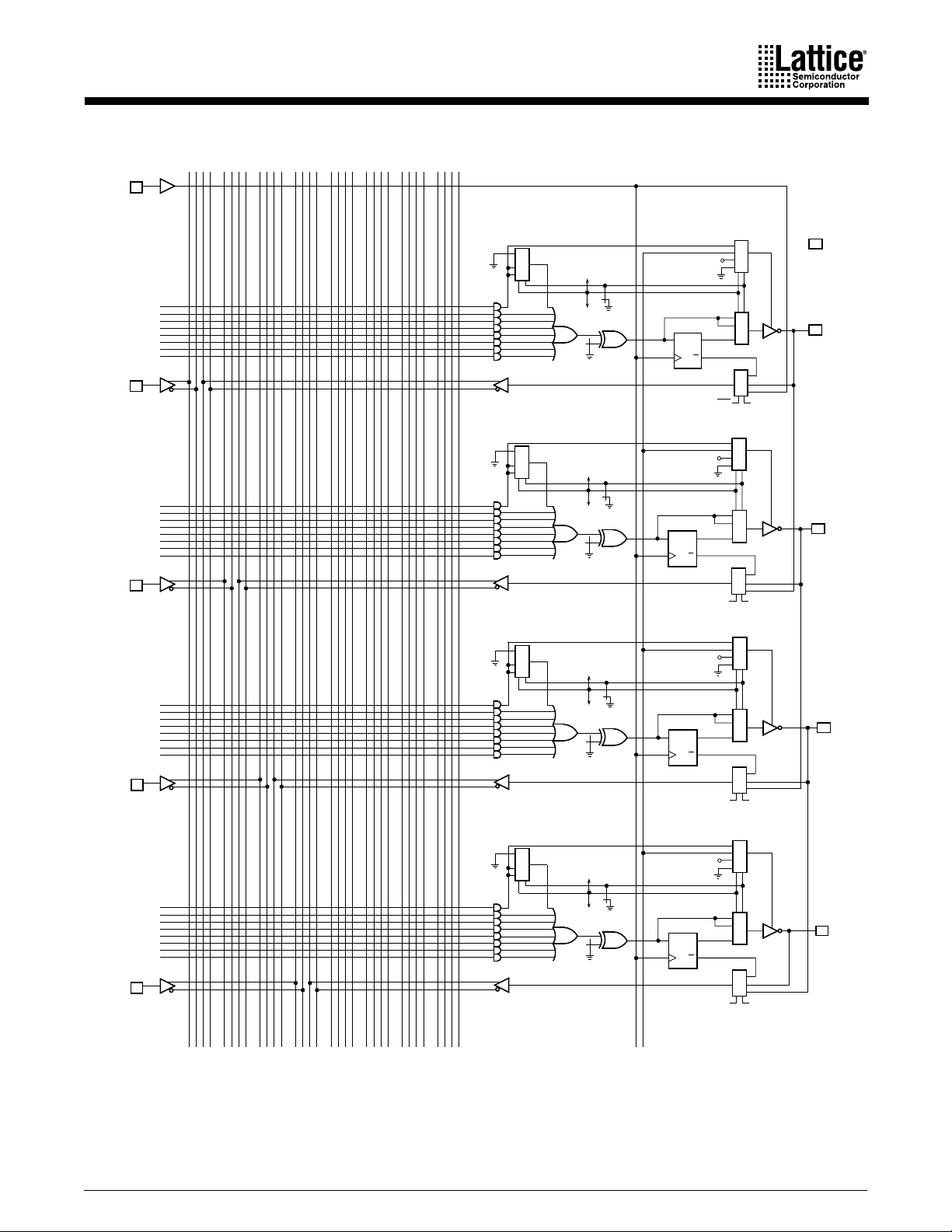
LOGIC DIAGRAM
034781112151619202324272831
CLK/I
1
0
1 1
1 1
0 X
1 0
SL0
0
7
I
2
1
1 1
0 X
1 0
8
15
I
3
2
1 1
0 X
1 0
16
23
4
I
3
SG1
SL1
SL1
SG1
SG1
SL1
7
DQ
7
SL0
6
DQ
6
SL0
5
5
Q
DQ
Q
NEW DESIGNS
1 0
0 0
V
CC
0 1
1 1
0 X
1 0
Q
1 0
1 1
0 X
SG0
SL0
1 1
1 0
0 0
V
CC
0 1
1 1
0 X
1 0
1 0
1 1
0 X
SG1
SL0
1 1
1 0
0 0
V
CC
0 1
1 1
0 X
1 0
1 0
1 1
0 X
SG1
SL0
20
V
CC
I/O
19
7
7
18
I/O
6
6
17
I/O
5
5
USE GAL DEVICES FOR
1 1
0 X
1 0
SL0
SL1
SG1
4
DQ
4
CLK OE
24
31
5
I
4
03478111215161920 2427283123
1 1
1 0
0 0
V
CC
0 1
1 1
0 X
1 0
Q
1 0
1 1
0 X
SG1
SL0
4
16
I/O
4
16493E-2
PALCE16V8 and PALCE16V8Z Families 9
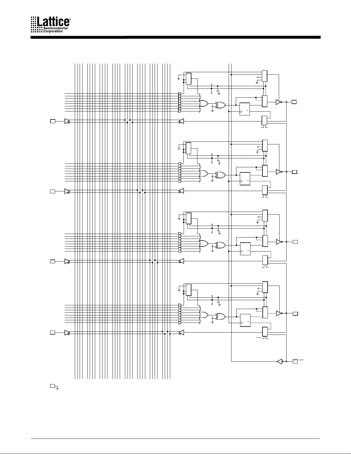
LOGIC DIAGRAM (CONTINUED)
034781112151619202324272831
1 1
0 X
1 0
32
39
6
I
5
1 1
0 X
1 0
40
47
7
I
6
1 1
0 X
1 0
48
55
8
I
7
SG1
SL1
SG1
SL1
SG1
SL1
CLK OE
1 1
1 0
0 0
V
CC
0 1
SL0
3
1 1
DQ
3
SL0
2
DQ
2
SL0
1
DQ
1
0 X
1 0
Q
1 0
1 1
0 X
SG1
SL0
3
1 1
1 0
0 0
V
CC
0 1
1 1
0 X
1 0
Q
1 0
1 1
0 X
SG1
SL0
2
1 1
1 0
0 0
V
CC
0 1
1 1
0 X
1 0
Q
1 0
1 1
0 X
SG1
SL0
1
15
I/O
3
14
I/O
2
13
I/O
1
1 1
0 X
1 0
SG1
SL1
0
I
8
GND 10
NEW DESIGNS
56
63
9
USE GAL DEVICES FOR
0 3 4 7 8 1112 15161920 2324 2728 31
10 PALCE16V8 and PALCE16V8Z Families
1 1
1 0
0 0
V
CC
0 1
SL0
0
1 1
DQ
Q
SG0
0 X
1 0
1 0
1 1
0 X
SL0
0
I/O012
11
OE/I
9
16493E-6
(concluded)

ABSOLUTE MAXIMUM RATINGS
OPERATING RANGES
Storage Temperature. . . . . . . . . . . . . .-65°C to +150°C
Ambient Temperature
with Power Applied . . . . . . . . . . . . . .-55°C to +125°C
Supply Voltage
with Respect to Ground . . . . . . . . . . -0.5 V to +7.0 V
DC Input Voltage . . . . . . . . . . . -0.5 V to V
CC
+ 0.5 V
DC Output or I/O
Commercial (C) Devices
Ambient Temperature (TA)
Operating in Free Air. . . . . . . . . . . . . . . 0°C to +75°C
Supply Voltage (VCC)
with Respect to Ground . . . . . . . . . +4.75 V to +5.25 V
Operating ranges define those limits between which the functionality of the device is guaranteed.
Pin Voltage. . . . . . . . . . . . . . . . .-0.5 V to VCC + 0.5 V
Static Discharge Voltage . . . . . . . . . . . . . . . . . 2001 V
Latchup Current (TA = 0°C to 75°C) . . . . . . . . .100 mA
Stresses above those listed under Absolute Maximum Ratings
may cause permanent device failure. Functionality at or above
these limits is not implied. Exposure to Absolute Maximum Ratings for extended periods may affect device reliability. Programming conditions may differ.
DC CHARACTERISTICS OVER COMMERCIAL OPERATING RANGES
Parameter
Symbol Parameter Description Test Description Min Max Unit
V
OH
V
OL
V
IH
Output HIGH Voltage IOH = -3.2 mA, VIN = VIH or VIL, VCC = Min 2.4 V
Output LOW Voltage IOL = 24 mA, VIN = VIH or VIL, VCC = Min 0.5 V
Input HIGH Voltage
Guaranteed Input Logical HIGH
Voltage for all Inputs (Note 1)
2.0 V
V
IL
I
IH
I
IL
Input LOW Voltage
Input HIGH Leakage Current VIN = 5.25 V, V
Input LOW Leakage Current VIN = 0 V, V
NEW DESIGNS
I
OZH
Off-State Output Leakage Current HIGH
USE GAL DEVICES FOR
I
OZL
I
SC
I
(Static) Supply Current for -5
CC
I
(Dynamic) Supply Current for -7
CC
Notes:
1. These are absolute values with respect to device ground, and all overshoots due to system or tester noise are included.
2. I/O pin leakage is the worst case of I
3. Not more than one output should be shorted at a time, and the duration of the short-circuit should not exceed one second.
V
OUT
Off-State Output Leakage Current LOW
Output Short-Circuit Current V
and I
IL
= 0.5 V has been chosen to avoid test problems caused by tester ground degradation.
(or IIH and I
OZL
Guaranteed Input Logical LOW
Voltage for all Inputs (Note 1)
= Max (Note 2) 10 µA
CC
= Max (Note 2) –100 µA
CC
= 5.25 V, VCC = Max
V
OUT
V
= V
or VIL (Note 2)
IN
IH
= 0 V, V
V
OUT
V
= V
IN
= 0.5 V, VCC = Max (Note 3) –30 –150 mA
OUT
Outputs Open (I
V
= Max
CC
Outputs Open (I
V
= Max, f = 25 MHz
CC
OZH
= Max
CC
or VIL (Note 2)
IH
OUT
OUT
).
= 0 mA), VIN = 0 V
= 0 mA),
0.8 V
10 µA
–100 µA
125 mA
115 mA
PALCE16V8H-5/7 (Com’l) 11

CAPACITANCE
Parameter
Symbol Parameter Description Test Conditions Typ Unit
1
C
IN
C
OUT
Note:
1. These parameters are not 100% tested, but are evaluated at initial characterization and at any time the design is modified where
capacitance may be affected.
SWITCHING CHARACTERISTICS OVER COMMERCIAL OPERATING RANGES
Parameter
Symbol Parameter Description
t
PD
t
S
t
H
t
CO
t
SKEWR
t
WL
t
WH
f
MAX
Input Capacitance V
Output Capacitance V
= 2.0 V VCC = 5.0 V, TA = 25 °C, 5 pF
IN
= 2.0 V f = 1 MHz 8 pF
OUT
1
-5 -7
2
Max Min
Input or Feedback to Combinatorial Output 1 5 3 7.5 ns
Setup Time from Input or Feedback to Clock 3 5 ns
Hold Time 0 0 ns
Clock to Output 1415ns
Skew Between Registered Outputs (Note 3) 1 1 ns
Clock Width
Maximum Frequency
(Note 4)
LOW 3 4 ns
HIGH 3 4 ns
External Feedback 1/(t
Internal Feedback (f
No Feedback 1/(tWH+tWL) 166 125 MHz
) 1/(tS+tCF) (Note 5) 166 125 MHz
CNT
) 142.8 100 MHz
S+tCO
2
Max
UnitMin
t
PZX
t
PXZ
t
EA
t
ER
Notes:
1. See “Switching Test Circuit” for test conditions.
2. Output delay minimums for t
may alter these values; therefore, minimum values are recommended for simulation purposes only.
3. Skew testing takes into account pattern and switching direction differences between outputs that have equal loading.
4. These parameters are not 100% tested, but are calculated at initial characterization and at any time the design is modified where
frequency may be affected.
is a calculated value and is not guaranteed. tCF can be found using the following equation:
5. t
CF
= 1/f
t
CF
OE to Output Enable 1616ns
OE to Output Disable 1516ns
Input to Output Enable Using Product Term Control 2639ns
Input to Output Disable Using Product Term Control 2539ns
NEW DESIGNS
USE GAL DEVICES FOR
(internal feedback) – tS.
MAX
PD
, tCO, t
PZX
, t
, tEA, and tER are defined under best case conditions. Future process improvements
PXZ
12 PALCE16V8H-5/7 (Com’l)

ABSOLUTE MAXIMUM RATINGS
OPERATING RANGES
Storage Temperature. . . . . . . . . . . . . .-65°C to +150°C
Ambient Temperature
with Power Applied . . . . . . . . . . . . . .-55°C to +125°C
Supply Voltage
with Respect to Ground . . . . . . . . . .-0.5 V to + 7.0 V
DC Input Voltage . . . . . . . . . . . -0.5 V to V
+ 0.5 V
CC
DC Output or I/O
Pin Voltage. . . . . . . . . . . . . . . . . -0.5 V to VCC + 0.5 V
Static Discharge Voltage . . . . . . . . . . . . . . . . . 2001 V
Latchup Current (TA = -40°C to +85°C). . . . . . . 100 mA
Stresses above those listed under Absolute Maximum Ratings
may cause permanent device failure. Functionality at or above
these limits is not implied. Exposure to Absolute Maximum Ratings for extended periods may affect device reliability. Programming conditions may differ.
Commercial (C) Devices
Ambient Temperature (TA)
Operating in Free Air. . . . . . . . . . . . . . . 0°C to +75°C
Supply Voltage (VCC)
with Respect to Ground . . . . . . . . . +4.75 V to +5.25 V
Industrial (I) Devices
Temperature (TA) Operating
in Free Air. . . . . . . . . . . . . . . . . . . . . . -40°C to +85°C
Supply Voltage (VCC)
with Respect to Ground . . . . . . . . . . . +4.5 V to +5.5 V
Operating ranges define those limits between which the functionality of the device is guaranteed.
DC CHARACTERISTICS OVER COMMERCIAL AND INDUSTRIAL OPERATING RANGES
Parameter
Symbol Parameter Description Test Description Min Max Unit
V
OH
V
OL
V
IH
V
IL
I
IH
I
IL
I
OZH
I
OZL
I
SC
I
(Dynamic)
CC
Notes:
1. These are absolute values with respect to device ground, and all overshoots due to system or tester noise are included.
2. I/O pin leakage is the worst case of I
3. Not more than one output should be shorted at a time, and the duration of the short-circuit should not exceed one second.
V
OUT
Output HIGH Voltage IOH = –3.2 mA, VIN = VIH or VIL, VCC = Min 2.4 V
Output LOW Voltage IOL = 24 mA, VIN = VIH or VIL, VCC = Min 0.5 V
Input HIGH Voltage
Input LOW Voltage
Input HIGH Leakage Current VIN = 5.25 V, V
Input LOW Leakage Current VIN = 0 V, V
Off-State Output Leakage Current HIGH
Off-State Output Leakage Current LOW
Output Short-Circuit Current V
Commercial Supply Current
Industrial Supply Current 130 mA
= 0.5 V has been chosen to avoid test problems caused by tester ground degradation.
USE GAL DEVICES FOR
and I
IL
NEW DESIGNS
(or IIH and I
OZL
Guaranteed Input Logical HIGH
Voltage for all Inputs (Note 1)
Guaranteed Input Logical LOW
Voltage for all Inputs (Note 1)
= Max (Note 2) 10 µA
CC
= Max (Note 2) –100 µA
CC
= 5.25 V, VCC = Max
V
OUT
V
= V
or VIL (Note 2)
IN
IH
= 0 V, V
V
OUT
V
= V
IN
= 0.5 V, VCC = Max (Note 3) –30 –150 mA
OUT
Outputs Open (I
V
= Max, f = 15 MHz
CC
OZH
= Max
CC
or VIL (Note 2)
IH
OUT
).
= 0 mA)
2.0 V
0.8 V
10 µA
–100 µA
115 mA
PALCE16V8H-10 (Com’l, Ind) 13
CAPACITANCE
Parameter
Symbol Parameter Description Test Conditions Typ Unit
1
C
IN
C
OUT
Note:
1. These parameters are not 100% tested, but are evaluated at initial characterization and at any time the design is modified where
capacitance may be affected.
Input Capacitance V
Output Capacitance V
= 2.0 V VCC = 5.0 V, TA = 25 °C, 5 pF
IN
= 2.0 V f = 1 MHz 8 pF
OUT
SWITCHING CHARACTERISTICS OVER COMMERCIAL AND INDUSTRIAL
OPERATING RANGES
Parameter
Symbol Parameter Description
t
t
t
t
t
t
f
PD
S
H
CO
WL
WH
MAX
Input or Feedback to Combinatorial Output 3 10 ns
Setup Time from Input or Feedback to Clock 7.5 ns
Hold Time 0ns
Clock to Output 3 7.5 ns
Clock Width
Maximum Frequency
(Note 3)
1
-10
2
Max
LOW 6 ns
HIGH 6 ns
External Feedback 1/(t
Internal Feedback (f
No Feedback 1/(tWH+tWL) 83.3 MHz
) 1/(tS+tCF) (Note 4) 71.4 MHz
CNT
) 66.7 MHz
S+tCO
UnitMin
t
PZX
t
PXZ
t
EA
t
ER
Notes:
1. See “Switching Test Circuit” for test conditions.
2. Output delay minimums for t
may alter these values; therefore, minimum values are recommended for simulation purposes only.
3. These parameters are not 100% tested, but are calculated at initial characterization and at any time the design is modified where
frequency may be affected.
is a calculated value and is not guaranteed. tCF can be found using the following equation:
4. t
CF
= 1/f
t
CF
OE to Output Enable 210ns
OE to Output Disable 210ns
Input to Output Enable Using Product Term Control 3 10 ns
Input to Output Disable Using Product Term Control 3 10 ns
NEW DESIGNS
USE GAL DEVICES FOR
(internal feedback) – tS.
MAX
PD
, tCO, t
PZX
, t
, tEA, and tER are defined under best case conditions. Future process improvements
PXZ
14 PALCE16V8H-10 (Com’l, Ind)

ABSOLUTE MAXIMUM RATINGS
OPERATING RANGES
Storage Temperature. . . . . . . . . . . . . .-65°C to +150°C
Ambient Temperature
with Power Applied . . . . . . . . . . . . . .-55°C to +125°C
Supply Voltage
with Respect to Ground . . . . . . . . . . -0.5 V to +7.0 V
DC Input Voltage . . . . . . . . . . . -0.5 V to V
CC
+ 0.5 V
DC Output or I/O
Commercial (C) Devices
Ambient Temperature (TA)
Operating in Free Air. . . . . . . . . . . . . . . 0°C to +75°C
Supply Voltage (VCC)
with Respect to Ground . . . . . . . . . +4.75 V to +5.25 V
Operating ranges define those limits between which the functionality of the device is guaranteed.
Pin Voltage. . . . . . . . . . . . . . . . .-0.5 V to VCC + 0.5 V
Static Discharge Voltage . . . . . . . . . . . . . . . . . 2001 V
Latchup Current (TA = 0°C to 75°C) . . . . . . . . .100 mA
Stresses above those listed under Absolute Maximum Ratings
may cause permanent device failure. Functionality at or above
these limits is not implied. Exposure to Absolute Maximum Ratings for extended periods may affect device reliability. Programming conditions may differ.
DC CHARACTERISTICS OVER COMMERCIAL OPERATING RANGES
Parameter
Symbol Parameter Description Test Description Min Max Unit
V
OH
V
OL
V
IH
Output HIGH Voltage IOH = -3.2 mA, VIN = VIH or VIL, VCC = Min 2.4 V
Output LOW Voltage IOL = 24 mA, VIN = VIH or VIL, VCC = Min 0.5 V
Input HIGH Voltage
Guaranteed Input Logical HIGH
Voltage for all Inputs (Note 1)
2.0 V
V
IL
I
IH
I
IL
Input LOW Voltage
Input HIGH Leakage Current VIN = 5.25 V, V
Input LOW Leakage Current VIN = 0 V, V
NEW DESIGNS
I
OZH
Off-State Output Leakage Current HIGH
USE GAL DEVICES FOR
I
OZL
I
SC
I
CC
Notes:
1. These are absolute values with respect to device ground, and all overshoots due to system or tester noise are included.
2. I/O pin leakage is the worst case of I
3. Not more than one output should be shorted at a time, and the duration of the short-circuit should not exceed one second.
V
OUT
Off-State Output Leakage Current LOW
Output Short-Circuit Current V
Supply Current (Dynamic)
and I
IL
= 0.5 V has been chosen to avoid test problems caused by tester ground degradation.
(or IIH and I
OZL
Guaranteed Input Logical LOW
Voltage for all Inputs (Note 1)
= Max (Note 2) 10 µA
CC
= Max (Note 2) –100 µA
CC
= 5.25 V, VCC = Max
V
OUT
V
= V
or VIL (Note 2)
IN
IH
= 0 V, V
V
OUT
V
= V
IN
= 0.5 V, VCC = Max (Note 3) –30 –150 mA
OUT
Outputs Open (I
V
= Max, f = 15 MHz
CC
OZH
= Max
CC
or VIL (Note 2)
IH
OUT
).
= 0 mA),
0.8 V
10 µA
–100 µA
55 mA
PALCE16V8Q-10 (Com’l) 15

CAPACITANCE
Parameter
Symbol Parameter Description Test Conditions Typ Unit
1
C
IN
C
OUT
Note:
1. These parameters are not 100% tested, but are evaluated at initial characterization and at any time the design is modified where
capacitance may be affected.
SWITCHING CHARACTERISTICS OVER COMMERCIAL OPERATING RANGES
Parameter
Symbol Parameter Description
t
PD
t
S
t
H
t
CO
t
WL
t
WH
f
MAX
Input Capacitance V
Output Capacitance V
= 2.0 V VCC = 5.0 V, TA = 25 °C, 5 pF
IN
= 2.0 V f = 1 MHz 8 pF
OUT
1
-10
2
Max
Input or Feedback to Combinatorial Output 3 10 ns
Setup Time from Input or Feedback to Clock 7.5 ns
Hold Time 0ns
Clock to Output 3 7.5 ns
Clock Width
Maximum Frequency
(Note 3)
LOW 6 ns
HIGH 6 ns
External Feedback 1/(t
Internal Feedback (f
No Feedback 1/(tWH+tWL) 83.3 MHz
) 1/(tS+tCF) (Note 4) 71.4 MHz
CNT
) 66.7 MHz
S+tCO
UnitMin
t
PZX
t
PXZ
t
EA
t
ER
OE to Output Enable 210ns
OE to Output Disable 210ns
Input to Output Enable Using Product Term Control 3 10 ns
Input to Output Disable Using Product Term Control 3 10 ns
NEW DESIGNS
Notes:
1. See “Switching Test Circuit” for test conditions.
2. Output delay minimums for t
may alter these values; therefore, minimum values are recommended for simulation purposes only.
3. These parameters are not 100% tested, but are calculated at initial characterization and at any time the design is modified where
frequency may be affected.
is a calculated value and is not guaranteed. tCF can be found using the following equation:
4. t
CF
t
CF
= 1/f
(internal feedback) – tS.
MAX
USE GAL DEVICES FOR
PD
, tCO, t
PZX
, t
, tEA, and tER are defined under best case conditions. Future process improvements
PXZ
16 PALCE16V8Q-10 (Com’l)

ABSOLUTE MAXIMUM RATINGS
OPERATING RANGES
Storage Temperature. . . . . . . . . . . . . .-65°C to +150°C
Ambient Temperature
with Power Applied . . . . . . . . . . . . . .-55°C to +125°C
Supply Voltage
with Respect to Ground . . . . . . . . . .-0.5 V to + 7.0 V
DC Input Voltage . . . . . . . . . . . -0.5 V to V
+ 0.5 V
CC
DC Output or I/O
Pin Voltage. . . . . . . . . . . . . . . . . -0.5 V to VCC + 0.5 V
Static Discharge Voltage . . . . . . . . . . . . . . . . . 2001 V
Latchup Current (TA = -40°C to +85°C). . . . . . . 100 mA
Stresses above those listed under Absolute Maximum Ratings
may cause permanent device failure. Functionality at or above
these limits is not implied. Exposure to Absolute Maximum Ratings for extended periods may affect device reliability. Programming conditions may differ.
Commercial (C) Devices
Ambient Temperature (TA)
Operating in Free Air. . . . . . . . . . . . . . . 0°C to +75°C
Supply Voltage (VCC)
with Respect to Ground . . . . . . . . . +4.75 V to +5.25 V
Industrial (I) Devices
Temperature (TA) Operating
in Free Air. . . . . . . . . . . . . . . . . . . . . . -40°C to +85°C
Supply Voltage (VCC)
with Respect to Ground . . . . . . . . . . . +4.5 V to +5.5 V
Operating ranges define those limits between which the functionality of the device is guaranteed.
DC CHARACTERISTICS OVER COMMERCIAL AND INDUSTRIAL OPERATING RANGES
Parameter
Symbol Parameter Description Test Description Min Max Unit
V
OH
V
OL
V
IH
V
IL
I
IH
I
IL
I
OZH
I
OZL
I
SC
I
(Dynamic)
CC
Notes:
1. These are absolute values with respect to device ground, and all overshoots due to system or tester noise are included.
2. I/O pin leakage is the worst case of I
3. Not more than one output should be shorted at a time, and the duration of the short-circuit should not exceed one second.
V
OUT
Output HIGH Voltage IOH = –3.2 mA, VIN = VIH or VIL, VCC = Min 2.4 V
Output LOW Voltage IOL = 24 mA, VIN = VIH or VIL, VCC = Min 0.5 V
Input HIGH Voltage
Input LOW Voltage
Input HIGH Leakage Current VIN = 5.25 V, V
Input LOW Leakage Current VIN = 0 V, V
Off-State Output Leakage Current HIGH
Off-State Output Leakage Current LOW
Output Short-Circuit Current V
Commercial Supply Current
Industrial Supply Current
= 0.5 V has been chosen to avoid test problems caused by tester ground degradation.
USE GAL DEVICES FOR
and I
IL
NEW DESIGNS
(or IIH and I
OZL
Guaranteed Input Logical HIGH
Voltage for all Inputs (Note 1)
Guaranteed Input Logical LOW
Voltage for all Inputs (Note 1)
= Max (Note 2) 10 µA
CC
= Max (Note 2) –100 µA
CC
= 5.25 V, VCC = Max
V
OUT
V
= V
or VIL (Note 2)
IN
IH
= 0 V, V
V
OUT
V
= V
IN
= 0.5 V, VCC = Max (Note 3) –30 –150 mA
OUT
Outputs Open (I
V
= Max, f = 15 MHz
CC
OZH
= Max
CC
or VIL (Note 2)
IH
OUT
).
= 0 mA)
H90
Q55
H 130
Q65
2.0 V
0.8 V
10 µA
–100 µA
mA
mA
PALCE16V8H-15/25 (Com’l, Ind), Q-15/25 (Com’l), Q-20/25 (Ind) 17
CAPACITANCE
Parameter
Symbol Parameter Description Test Conditions Typ Unit
1
C
IN
C
OUT
Note:
1. These parameters are not 100% tested, but are evaluated at initial characterization and at any time the design is modified where
capacitance may be affected.
Input Capacitance V
Output Capacitance V
= 2.0 V VCC = 5.0 V, TA = 25 °C, 5 pF
IN
= 2.0 V f = 1 MHz 8 pF
OUT
SWITCHING CHARACTERISTICS OVER COMMERCIAL AND INDUSTRIAL
OPERATING RANGES
Parameter
Symbol Parameter Description
t
PD
t
S
t
H
t
CO
t
WL
t
WH
f
MAX
t
PZX
t
PXZ
t
EA
t
ER
Notes:
1. See “Switching Test Circuit” for test conditions.
2. These parameters are not 100% tested, but are calculated at initial characterization and at any time the design is modified where
frequency may be affected.
Input or Feedback to Combinatorial Output 15 20 25 ns
Setup Time from Input or Feedback to Clock 12 13 15 ns
Hold Time 0 0 0 ns
Clock to Output 10 11 12 ns
Clock Width
Maximum
Frequency
(Note 2)
OE to Output Enable 15 18 20 ns
OE to Output Disable 15 18 20 ns
Input to Output Enable Using Product Term Control 15 18 20 ns
Input to Output Disable Using Product Term Control 15 18 20 ns
USE GAL DEVICES FOR
1
-15 -20 -25
UnitMin Max Min Max Min Max
LOW 8 10 12 ns
HIGH 8 10 12 ns
External Feedback 1/(t
Internal Feedback
(f
)
CNT
No Feedback 1/(t
) 45.5 41.6 37 MHz
S+tCO
)
1/(t
S+tCF
(Note 3)
WH+tWL
50 45.4 40 MHz
) 62.5 50.0 41.6 MHz
NEW DESIGNS
3. t
is a calculated value and is not guaranteed. tCF can be found using the following equation:
CF
t
CF
= 1/f
(internal feedback) – tS.
MAX
18 PALCE16V8H-15/25 (Com’l, Ind), Q-15/25 (Com’l), Q-20/25 (Ind)

ABSOLUTE MAXIMUM RATINGS
OPERATING RANGES
Storage Temperature. . . . . . . . . . . . . .-65°C to +150°C
Ambient Temperature
with Power Applied . . . . . . . . . . . . . .-55°C to +125°C
Supply Voltage
with Respect to Ground . . . . . . . . . .-0.5 V to + 7.0 V
DC Input Voltage . . . . . . . . . . . -0.5 V to V
+ 0.5 V
CC
DC Output or I/O Pin Voltage . . .-0.5 V to VCC + 0.5 V
Industrial (I) Devices
Ambient Temperature (TA)
Operating in Free Air. . . . . . . . . . . . . . -40°C to +85°C
Supply Voltage (VCC)
with Respect to Ground . . . . . . . . . . . +4.5 V to +5.5 V
Operating ranges define those limits between which the functionality of the device is guaranteed.
Static Discharge Voltage . . . . . . . . . . . . . . . . . 2001 V
Latchup Current (TA = -40°C to +85°C). . . . . . . 100 mA
Stresses above those listed under Absolute Maximum Ratings
may cause permanent device failure. Functionality at or above
these limits is not implied. Exposure to Absolute Maximum Ratings for extended periods may affect device reliability. Programming conditions may differ.
DC CHARACTERISTICS OVER INDUSTRIAL OPERATING RANGES
Parameter
Symbol Parameter Description Test Description Min Max Unit
= 6 mA 3.84 V
I
V
V
V
V
I
I
I
I
I
I
OH
OL
IH
IL
IH
IL
OZH
OZL
SC
CC
Output HIGH Voltage VIN = VIH or VIL, VCC = Min
Output LOW Voltage VIN = VIH or VIL, VCC = Min
Input HIGH Voltage
Input LOW Voltage
Input HIGH Leakage Current VIN = 5.25 V, V
Input LOW Leakage Current VIN = 0 V, V
Off-State Output Leakage Current HIGH
Off-State Output Leakage Current LOW
Output Short-Circuit Current V
Supply Current (Static)
Supply Current
USE GAL DEVICES FOR
(Dynamic) f = 15 MHz 75 mA
Guaranteed Input Logical HIGH
Voltage for all Inputs (Notes 1 and 2)
Guaranteed Input Logical LOW
Voltage for all Inputs (Notes 1 and 2)
= Max (Note 3) 10 µA
CC
NEW DESIGNS
V
OUT
V
= V
IN
V
OUT
V
= V
IN
OUT
Outputs Open (I
V
= Max
CC
= Max (Note 3) –10 µA
CC
= 5.25 V, VCC = Max
or VIL (Note 3)
IH
= 0 V, V
= 0.5 V, VCC = Max (Note 4) –30 –150 mA
= Max
CC
or VIL (Note 3)
IH
OUT
= 0 mA)
OH
= 20 µA VCC – 0.1 V V
I
OH
I
= 24 mA 0.5 V
OL
= 6 mA 0.33 V
I
OL
= 20 µA 0.1 V
I
OL
2.0 V
0.9 V
10 µA
–10 µA
f = 0 MHz 30 µA
Notes:
1. These are absolute values with respect to device ground, and all overshoots due to system or tester noise are included.
2. Represents the worst case of HC and HCT standards, allowing compatibility with either.
3. I/O pin leakage is the worst case of I
4. Not more than one output should be shorted at a time, and the duration of the short-circuit should not exceed one second.
= 0.5 V has been chosen to avoid test problems caused by tester ground degradation.
V
OUT
and I
IL
(or IIH and I
OZL
OZH
).
PALCE16V8Z-12 (Ind) 19

CAPACITANCE
Parameter
Symbol Parameter Description Test Conditions Typ Unit
1
C
IN
C
OUT
Note:
1. These parameters are not 100% tested, but are evaluated at initial characterization and at any time the design is modified where
capacitance may be affected.
SWITCHING CHARACTERISTICS OVER INDUSTRIAL OPERATING RANGES
Parameter
Symbol Parameter Description
t
PD
t
S
t
H
t
CO
t
WL
t
WH
f
MAX
Input Capacitance V
Output Capacitance V
= 2.0 V VCC = 5.0 V, TA = 25 °C, 5 pF
IN
= 2.0 V f = 1 MHz 8 pF
OUT
1
-12
UnitMin Max
Input or Feedback to Combinatorial Output (Note 2) 12 ns
Setup Time from Input or Feedback to Clock 8ns
Hold Time 0ns
Clock to Output 8ns
Clock Width
Maximum Frequency
(Notes 3 and 4)
LOW 5ns
HIGH 5ns
External Feedback 1/(t
Internal Feedback (f
No Feedback 1/(tWH+tWL) 100 MHz
) 1/(tS+tCF) 77 MHz
CNT
) 62.5 MHz
S+tCO
t
PZX
t
PXZ
t
EA
t
ER
OE to Output Enable 8ns
OE to Output Disable 8ns
Input to Output Enable Using Product Term Control 13 ns
Input to Output Disable Using Product Term Control 13 ns
NEW DESIGNS
Notes:
1. See “Switching Test Circuit” for test conditions.
2. This parameter is tested in standby mode.
3. These parameters are not 100% tested, but are calculated at initial characterization and at any time the design is modified where
frequency may be affected.
4. Output delay minimums for t
may alter these values therefore, minimum values are recommended for simulation purposes only.
is a calculated value and is not guaranteed. tCF can be found using the following equation:
5. t
CF
t
CF
= 1/f
(internal feedback) – tS.
MAX
USE GAL DEVICES FOR
PD
, tCO, t
PZX
, t
, tEA, and tER are defined under best case conditions. Future process improvements
PXZ
20 PALCE16V8Z-12 (Ind)

ABSOLUTE MAXIMUM RATINGS
OPERATING RANGES
Storage Temperature. . . . . . . . . . . . . .-65°C to +150°C
Ambient Temperature
with Power Applied . . . . . . . . . . . . . .-55°C to +125°C
Supply Voltage
with Respect to Ground . . . . . . . . . .-0.5 V to + 7.0 V
DC Input Voltage . . . . . . . . . . . -0.5 V to V
+ 0.5 V
CC
DC Output or I/O Pin Voltage . . .-0.5 V to VCC + 0.5 V
Industrial (I) Devices
Ambient Temperature (TA)
Operating in Free Air. . . . . . . . . . . . . . -40°C to +85°C
Supply Voltage (VCC)
with Respect to Ground . . . . . . . . . . . +4.5 V to +5.5 V
Operating ranges define those limits between which the functionality of the device is guaranteed.
Static Discharge Voltage . . . . . . . . . . . . . . . . . 2001 V
Latchup Current (TA = -40°C to +85°C). . . . . . . 100 mA
Stresses above those listed under Absolute Maximum Ratings
may cause permanent device failure. Functionality at or above
these limits is not implied. Exposure to Absolute Maximum Ratings for extended periods may affect device reliability. Programming conditions may differ.
DC CHARACTERISTICS OVER INDUSTRIAL OPERATING RANGES
Parameter
Symbol Parameter Description Test Description Min Max Unit
= 6 mA 3.84 V
I
V
V
V
V
I
I
I
I
I
I
OH
OL
IH
IL
IH
IL
OZH
OZL
SC
CC
Output HIGH Voltage VIN = VIH or VIL, VCC = Min
Output LOW Voltage VIN = VIH or VIL, VCC = Min
Input HIGH Voltage
Input LOW Voltage
Input HIGH Leakage Current VIN = 5.25 V, V
Input LOW Leakage Current VIN = 0 V, V
Off-State Output Leakage Current HIGH
Off-State Output Leakage Current LOW
Output Short-Circuit Current V
Supply Current (Static)
Supply Current
USE GAL DEVICES FOR
(Dynamic) f = 25 MHz 75 mA
Guaranteed Input Logical HIGH
Voltage for all Inputs (Notes 1 and 2)
Guaranteed Input Logical LOW
Voltage for all Inputs (Notes 1 and 2)
= Max (Note 3) 10 µA
CC
NEW DESIGNS
V
OUT
V
= V
IN
V
OUT
V
= V
IN
OUT
Outputs Open (I
V
= Max
CC
= Max (Note 3) –10 µA
CC
= 5.25 V, VCC = Max
or VIL (Note 3)
IH
= 0 V, V
= 0.5 V, VCC = Max (Note 4) –30 –150 mA
= Max
CC
or VIL (Note 3)
IH
OUT
= 0 mA)
OH
= 20 µA VCC – 0.1 V V
I
OH
I
= 24 mA 0.5 V
OL
= 6 mA 0.33 V
I
OL
= 20 µA 0.1 V
I
OL
2.0 V
0.9 V
10 µA
–10 µA
f = 0 MHz 15 µA
Notes:
1. These are absolute values with respect to device ground, and all overshoots due to system or tester noise are included.
2. Represents the worst case of HC and HCT standards, allowing compatibility with either.
3. I/O pin leakage is the worst case of I
4. Not more than one output should be shorted at a time, and the duration of the short-circuit should not exceed one second.
= 0.5 V has been chosen to avoid test problems caused by tester ground degradation.
V
OUT
and I
IL
(or IIH and I
OZL
OZH
).
PALCE16V8Z-15 (Ind) 21

CAPACITANCE
Parameter
Symbol Parameter Description Test Conditions Typ Unit
1
C
IN
C
OUT
Note:
1. These parameters are not 100% tested, but are evaluated at initial characterization and at any time the design is modified where
capacitance may be affected.
SWITCHING CHARACTERISTICS OVER INDUSTRIAL OPERATING RANGES
Parameter
Symbol Parameter Description
t
PD
t
S
t
H
t
CO
t
WL
t
WH
f
MAX
Input Capacitance V
Output Capacitance V
= 2.0 V VCC = 5.0 V, TA = 25 °C, 5 pF
IN
= 2.0 V f = 1 MHz 8 pF
OUT
1
-15
2
Max
Input or Feedback to Combinatorial Output 15 ns
Setup Time from Input or Feedback to Clock 10 ns
Hold Time 0ns
Clock to Output 10 ns
Clock Width
Maximum
Frequency (Notes 3
and 4)
LOW 8 ns
HIGH 8 ns
External Feedback 1/(t
Internal Feedback (f
No Feedback 1/(tWH+tWL) 62.5 MHz
) 1/(tS+tCF) 58.8 MHz
CNT
) 50 MHz
S+tCO
UnitMin
t
PZX
t
PXZ
t
EA
t
ER
OE to Output Enable 15 ns
OE to Output Disable 15 ns
Input to Output Enable Using Product Term Control 15 ns
Input to Output Disable Using Product Term Control 15 ns
NEW DESIGNS
Notes:
1. See “Switching Test Circuit” for test conditions.
2. This parameter is tested in standby mode.
3. These parameters are not 100% tested, but are calculated at initial characterization and at any time the design is modified where
frequency may be affected.
4. t
is a calculated value and is not guaranteed. tCF can be found using the following equation:
CF
t
CF
= 1/f
(internal feedback) – tS.
MAX
USE GAL DEVICES FOR
22 PALCE16V8Z-15 (Ind)

ABSOLUTE MAXIMUM RATINGS
OPERATING RANGES
Storage Temperature. . . . . . . . . . . . . .-65°C to +150°C
Ambient Temperature
with Power Applied . . . . . . . . . . . . . .-55°C to +125°C
Supply Voltage
with Respect to Ground . . . . . . . . . .-0.5 V to + 7.0 V
DC Input Voltage . . . . . . . . . . . -0.5 V to V
+ 0.5 V
CC
DC Output or I/O Pin Voltage . . .-0.5 V to VCC + 0.5 V
Static Discharge Voltage . . . . . . . . . . . . . . . . . 2001 V
Latchup Current (TA = -40°C to +85°C). . . . . . . 100 mA
Stresses above those listed under Absolute Maximum Ratings
may cause permanent device failure. Functionality at or above
these limits is not implied. Exposure to Absolute Maximum Ratings for extended periods may affect device reliability. Programming conditions may differ.
Commercial (C) Devices
Ambient Temperature (TA)
Operating in Free Air. . . . . . . . . . . . . . . 0°C to +75°C
Supply Voltage (VCC)
with Respect to Ground . . . . . . . . . +4.75 V to +5.25 V
Industrial (I) Devices
Temperature (TA) Operating
in Free Air. . . . . . . . . . . . . . . . . . . . . . -40°C to +85°C
Supply Voltage (VCC)
with Respect to Ground . . . . . . . . . . . +4.5 V to +5.5 V
Operating ranges define those limits between which the functionality of the device is guaranteed.
DC CHARACTERISTICS OVER COMMERCIAL AND INDUSTRIAL OPERATING RANGES
Parameter
Symbol Parameter Description Test Description Min Max Unit
= 6 mA 3.84 V
I
V
V
V
V
I
I
I
I
I
I
OH
OL
IH
IL
IH
IL
OZH
OZL
SC
CC
Output HIGH Voltage VIN = VIH or VIL, VCC = Min
Output LOW Voltage VIN = VIH or VIL, VCC = Min
Input HIGH Voltage
Input LOW Voltage
Input HIGH Leakage Current VIN = 5.25 V, V
Input LOW Leakage Current VIN = 0 V, V
Off-State Output Leakage Current HIGH
Off-State Output Leakage Current LOW
Output Short-Circuit Current V
Supply Current (Static)
Supply Current
USE GAL DEVICES FOR
(Dynamic) f = 25 MHz 90 mA
Guaranteed Input Logical HIGH
Voltage for all Inputs (Notes 1 and 2)
Guaranteed Input Logical LOW
Voltage for all Inputs (Notes 1 and 2)
NEW DESIGNS
= 5.25 V, VCC = Max
V
OUT
V
= V
IN
IH
= 0 V, V
V
OUT
V
= V
IN
IH
= 0.5 V, VCC = Max (Note 4) –30 –150 mA
OUT
Outputs Open (I
V
= Max
CC
= Max (Note 3) 10 µA
CC
= Max (Note 3) –10 µA
CC
or VIL (Note 3)
= Max
CC
or VIL (Note 3)
= 0 mA)
OUT
OH
= 20 µA VCC – 0.1 V V
I
OH
I
= 24 mA 0.5 V
OL
= 6 mA 0.33 V
I
OL
= 20 µA 0.1 V
I
OL
2.0 V
0.9 V
10 µA
–10 µA
f = 0 MHz 15 µA
Notes:
1. These are absolute values with respect to device ground, and all overshoots due to system or tester noise are included.
2. Represents the worst case of HC and HCT standards, allowing compatibility with either.
3. I/O pin leakage is the worst case of I
4. Not more than one output should be shorted at a time, and the duration of the short-circuit should not exceed one second.
= 0.5 V has been chosen to avoid test problems caused by tester ground degradation.
V
OUT
and I
IL
(or IIH and I
OZL
OZH
).
PALCE16V8Z-25 (Com’l, Ind) 23

CAPACITANCE
Parameter
Symbol Parameter Description Test Conditions Typ Unit
1
C
IN
C
OUT
Note:
1. These parameters are not 100% tested, but are evaluated at initial characterization and at any time the design is modified where
capacitance may be affected.
Input Capacitance V
Output Capacitance V
= 2.0 V VCC = 5.0 V, TA = 25 °C, 5 pF
IN
= 2.0 V f = 1 MHz 8 pF
OUT
SWITCHING CHARACTERISTICS OVER COMMERCIAL AND INDUSTRIAL
OPERATING RANGES
Parameter
Symbol Parameter Description
t
t
t
t
t
t
f
PD
S
H
CO
WL
WH
MAX
Input or Feedback to Combinatorial Output (Note 3) 25 ns
Setup Time from Input or Feedback to Clock 20 ns
Hold Time 0ns
Clock to Output 10 ns
Clock Width
Maximum
Frequency (Notes 4
and 5)
1
-25
2
Max
LOW 8ns
HIGH 8ns
External Feedback 1/(t
Internal Feedback (f
No Feedback 1/(tWH+tWL) 50 MHz
) 1/(tS+tCF) 50 MHz
CNT
) 33.3 MHz
S+tCO
UnitMin
t
PZX
t
PXZ
t
EA
t
ER
Notes:
1. See “Switching Test Circuit” for test conditions.
2. This parameter is tested in standby mode.
3. This parameter is tested in Standby Mode. When the device is not in Standby Mode, the t
4. These parameters are not 100% tested, but are calculated at initial characterization and at any time the design is modified where
frequency may be affected.
5. t
is a calculated value and is not guaranteed. tCF can be found using the following equation:
CF
= 1/f
t
CF
OE to Output Enable 25 ns
OE to Output Disable 25 ns
Input to Output Enable Using Product Term Control 25 ns
Input to Output Disable Using Product Term Control 25 ns
NEW DESIGNS
USE GAL DEVICES FOR
will typically be 2 ns faster.
PD
(internal feedback) – tS.
MAX
24 PALCE16V8Z-25 (Com’l, Ind)

SWITCHING WAVEFORMS
V
T
Input or
Feedback
Registered
Output
b. Registered output
t
S
t
CO
V
T
t
H
V
T
Clock
16493E-5
V
T
V
T
Input
Output
d. Input to output disable/enable
t
ER
t
EA
V
OH
– 0.5V
V
OL
+ 0.5V
16493E-6
Input or
Feedback
Combinatorial
Output
Clock
V
T
t
PD
a. Combinatorial output
t
WH
t
WL
c. Clock width
OE
Output
V
T
16493E-3
V
16493E-4
T
t
PXZ
V
V
OH
OL
– 0.5V
+ 0.5V
V
T
t
PZX
V
T
Notes:
1. V
= 1.5 V
T
2. Input pulse amplitude 0 V to 3.0 V.
3. Input rise and fall times 2 ns to 5 ns typical.
USE GAL DEVICES FOR
16493E-7
NEW DESIGNS
e. OE to output disable/enable
PALCE16V8 and PALCE16V8Z Families 25
KEY TO SWITCHING WAVEFORMS
5 V
WAVEFORM INPUTS OUTPUTS
SWITCHING TEST CIRCUIT
Must be
Steady
May
Change
from H to L
May
Change
from L to H
Don’t Care,
Any Change
Permitted
Does Not
Apply
Will be
Steady
Will be
Changing
from H to L
Will be
Changing
from L to H
Changing,
State
Unknown
Center
Line is HighImpedance
“Off” State
KS000010-PAL
Specification S
tPD, t
CO
t
EA
t
ER
S
1
R
1
NEW DESIGNS
Output
Test Point
USE GAL DEVICES FOR
R
2
1
Closed
Z → H: Open
Z → L: Closed
H → Z: Open
L → Z: Closed L → Z: V
C
L
50 pF
5 pF H-5: 200 Ω
1
200 Ω
C
L
Commercial
R
2
390 Ω
16493E-8
Measured Output ValueR
1.5 V
1.5 V
H → Z: VOH – 0.5 V
+ 0.5 V
OL
26 PALCE16V8 and PALCE16V8Z Families

TYPICAL ICC CHARACTERISTICS
VCC = 5 V, TA = 25°C
150
(mA)
CC
I
125
100
75
50
25
0
01020304050
USE GAL DEVICES FOR
NEW DESIGNS
16V8H-5
16V8H-7
16V8H-10
16V8H-15/25
16V8Z-12/15
16V8Q-10/15/25
16V8Z-25
Frequency (MHz)
ICC vs. Frequency
The selected “typical” pattern utilized 50% of the device resources. Half of the macrocells were programmed as registered, and the
other half were programmed as combinatorial. Half of the available product terms were used for each macrocell. On any vector, half
of the outputs were switching.
By utilizing 50% of the device, a midpoint is defined for I
estimate the I
requirements for a particular design.
CC
PALCE16V8 and PALCE16V8Z Families 27
. From this midpoint, a designer may scale the ICC graphs up or down to
CC
16493E-9

ENDURANCE CHARACTERISTICS
The P ALCE16V8 is manufactured using Vantis’ advanced electrically-erasable (EE) CMOS process.
This technology uses an EE cell to replace the fuse link used in bipolar parts. As a result, the
device can be erased and reprogrammed—a feature which allows 100% testing at the factory.
Symbol Parameter Test Conditions Value Unit
t
DR
N Min Reprogramming Cycles Normal Programming Conditions 100 Cycles
Min Pattern Data Retention Time
Max Storage Temperature 10 Years
Max Operating Temperature 20 Years
ROBUSTNESS FEATURES
PALCE16V8X-X/5 devices have some unique features that make them extremely robust,
especially when operating in high-speed design environments. Pull-up resistors on inputs and
I/O pins cause unconnected pins to default to a known state. Input clamping circuitry limits
negative overshoot, eliminating the possibility of false clocking caused by subsequent ringing.
A special noise filter makes the programming circuitry completely insensitive to any positive
overshoot that has a pulse width of less than about 100 ns for the /5 versions. Selected /4 devices
are also being retrofitted with these robustness features.
INPUT/OUTPUT EQUIVALENT SCHEMATICS FOR PALCE16V8
V
C
C
> 50 kΩ
V
CC
ESD
Protection
and
Clamping
USE GAL DEVICES FOR
28 PALCE16V8 and PALCE16V8Z Families
Programming
Pins Only
NEW DESIGNS
V
CC
Provides ESD
Protection and
Clamping
Programming
Voltage
Detection
Typical Input
Typical Output
V
CC
> 50 kΩ
Preload
Circuitry
Positive
Overshoot
Filter
Feedback
Input
Programming
Circuitry
16493E-10

INPUT/OUTPUT EQUIVALENT SCHEMATICS FOR PALCE16V8Z
V
CC
ESD
Protection
and
Clamping
Input
Transition
Detection
Programming
Pins Only
Programming
Voltage
Detection
Positive
Overshoot
Filter
Programming
Circuitry
Typical Input
V
CC
Provides ESD
Protection and
Clamping
Preload
Circuitry
Feedback
Input
Input
Transition
Detection
16493E-11
Typical Output
POWER-UP RESET
The PALCE16V8 has been designed with the capability to reset during system power-up.
Following power-up, all flip-flops will be reset to LOW. The output state will be HIGH
independent of the logic polarity. This feature provides extra flexibility to the designer and is
especially valuable in simplifying state machine initialization. A timing diagram and parameter
table are shown below. Due to the synchronous operation of the power-up reset and the wide
range of ways V
USE GAL DEVICES FOR
can rise to its steady state, two conditions are required to ensure a valid
CC
power-up reset. These conditions are:
NEW DESIGNS
◆ The V
rise must be monotonic.
CC
◆ Following reset, the clock input must not be driven from LOW to HIGH until all applicable input
and feedback setup times are met.
Parameter Symbol Parameter Descriptions Min Max Unit
t
PR
t
S
t
WL
Power-Up Reset Time 1000 ns
Input or Feedback Setup Time
See Switching Characteristics
Clock Width LOW
PALCE16V8 and PALCE16V8Z Families 29

4 V
Power
t
PR
Registered
Output
Clock
t
WL
t
S
Figure 3. Power-Up Reset Waveform
TYPICAL THERMAL CHARACTERISTICS
Measured at 25°C ambient. These parameters are not tested.
V
CC
16493E-12
Parameter
Symbol Parameter Description
θ
jc
θ
ja
θ
jma
Plastic
The data listed for plastic
heat-flow paths in plastic-encapsulated devices are complex, making the
age surface. Tests indicate this measurement reference point is directly below the die-attach area on the bottom center of the package.
Furthermore,
perature. Therefore, the measurements can only be used in a similar environment.
θ
Thermal impedance, junction to case 25 22 °C/W
Thermal impedance, junction to ambient 71 64 °C/W
200 lfpm air 61 55 °C/W
Thermal impedance, junction to ambient with air flow
Considerations
jc
θ
are for reference only and are not recommended for use in calculating junction temperatures. The
jc
NEW DESIGNS
400 lfpm air 55 51 °C/W
600 lfpm air 51 47 °C/W
800 lfpm air 47 45 °C/W
θ
measurement relative to a specific location on the pack-
jc
USE GAL DEVICES FOR
θ
tests on packages are performed in a constant-temperature bath, keeping the package surface at a constant tem-
jc
Typ
UnitPDID PLCC
30 PALCE16V8 and PALCE16V8Z Families

CONNECTION DIAGRAMS
1
20
19
18
17
16
15
14
2
3
4
5
6
7
8
9
10 11 12 13
I
3
I
4
I
5
I
6
I
7
I/O
6
I/O
5
I/O
4
I/O
3
I/O
2
OE/I
9
I/O
0
I/O
1
GND
I
8
CLK/I
0
V
CC
I/O
7
I
1
I
2
16493E-10
Top View
DIP/SOIC
CLK/I
GND
Note:
Pin 1 is marked for orientation.
1
0
2
I
1
3
I
2
4
I
3
5
I
4
6
I
5
7
I
6
8
I
7
9
I
8
10
PIN DESIGNATIONS
20
19
18
17
16
15
14
13
12
11
V
CC
I/O
I/O
I/O
I/O
I/O
I/O
I/O
I/O
OE/I
PLCC
7
6
5
4
3
2
1
0
9
16493E-9
CLK = Clock
GND = Ground
I = Input
I/O = Input/Output
OE = Output Enable
V
= Supply Voltage
CC
NEW DESIGNS
USE GAL DEVICES FOR
PALCE16V8 and PALCE16V8Z Families 31

ORDERING INFORMATION
Commercial and Industrial Products
Lattice/V antis programmable logic products for commercial and industrial applications are available with several ordering options.
The order number (Valid Combination) is formed by a combination of:
FAMILY TYPE
PAL = Programmable Array Logic
TECHNOLOGY
CE = CMOS Electrically Erasable
NUMBER OF
ARRAY INPUTS
OUTPUT TYPE
V = Versatile
NUMBER OF OUTPUTS
POWER
H = Half Power (90–125 mA I
Q = Quarter Power (55 mA I
Z = Zero Power (15 µA I
SPEED
-5 = 5 ns t
-7 = 7.5 ns t
-10 = 10 ns t
-12 = 12 ns t
-15 = 15 ns t
-20 = 20 ns t
-25 = 25 ns t
PD
PD
PD
PD
PD
PD
PD
CC
Standby)
CC
PAL CE 16 V 8 H -5 J C
)
CC
)
/5
PROGRAMMING DESIGNATOR
Blank = Initial Algorithm
/4 = First Revision
/5 = Second Revision
(Same Algorithm as /4)
OPERATING CONDITIONS
C = Commercial (0
I = Industrial (-40
PACKAGE TYPE
P = 20-Pin Plastic DIP (PD 020)
J = 20-Pin Plastic Leaded Chip
Carrier (PL 020)
S = 20-Pin Plastic Gull-Wing
Small Outline Package (SO 020)
°C to +75°C)
°C to +85°C)
Valid Combinations
PALCE16V8H-5 JC
PALCE16V8H-7 PC, JC, SC
PALCE16V8H-10 PC, JC, SC, PI, JI /4
PALCE16V8Q-10 JC /5
PALCE16V8H-15 PC, JC, SC
PALCE16V8Q-15 PC, JC
PALCE16V8Q-20 PI, JI
PALCE16V8H-25 PC, JC, SC, PI, JI
PALCE16V8Q-25 PC, JC, PI, JI
PALCE16V8Z-12
PALCE16V8Z-15
PALCE16V8Z-25 PC, JC, SC, PI, JI, SI
USE GAL DEVICES FOR
PI, JI
NEW DESIGNS
Valid Combinations
Valid Combinations lists configurations planned to be
/5
/4
supported in volume for this device. Consult the local Lattice/
Vantis sales office to confirm availability of specific valid
combinations and to check on newly released combinations.
32 PALCE16V8 and PALCE16V8Z Families
 Loading...