

Page 1

Technical Note
TN1314 Version 1.0
June 2016
iCE40 SPRAM Usage Guide
Page 2

iCE40 SPRAM Usage Guide
Technical Note
Contents
Introduction .................................................................................................................................................................. 3 1.
Single Port RAM Primitives ........................................................................................................................................... 3 2.
2.1. User Primitive SB_SPRAM256KA ......................................................................................................................... 3
2.2. SPRAM Port Definitions and GUI Options ........................................................................................................... 4
Power Save States for SPRAM ...................................................................................................................................... 6 3.
3.1. Normal State ....................................................................................................................................................... 6
3.2. Standby State ...................................................................................................................................................... 6
3.3. Sleep State ........................................................................................................................................................... 6
3.4. Power Off State ................................................................................................................................................... 6
Use Cases for User Primitive SB_SPRAM256KA ............................................................................................................ 7 4.
4.1. Instantiating Memories ....................................................................................................................................... 7
4.2. Inferring Memories ............................................................................................................................................. 7
4.3. Output Pipeline Registers .................................................................................................................................... 7
4.4. Cascading Memories ........................................................................................................................................... 8
Address Cascading (or Depth Cascading) ........................................................................................................ 8 4.4.1.
Data Cascading (or Width Cascading) ............................................................................................................. 9 4.4.2.
Technical Support Assistance ............................................................................................................................................. 10
Revision History .................................................................................................................................................................. 11
Figures
Figure 2.1. SB_SPRAM256KA SPRAM Primitive .................................................................................................................... 3
Figure 4.1. Address/Depth Cascading Example for 32K x 16 SPRAM using Primitive ........................................................... 8
Figure 4.2. Data/Width Cascading Example for 16K x 32 SPRAM using Primitive ................................................................ 9
Tables
Table 2.1. SB_SPRAM256KA RAM Port Definitions .............................................................................................................. 4
© 2016 Lattice Semiconductor Corp. All Lattice trademarks, registered trademarks, patents, and disclaimers are as listed at www.latticesemi.com/legal. All other brand or product names are
2 TN1314-1.0
trademarks or registered trademarks of their respective holders. The specifications and information herein are subject to change without notice.
Page 3
iCE40 SPRAM Usage Guide
ADDRESS [13:0]
DATAIN [15:0]
WREN
MASKWREN [3:0]
CHIPSELECT
CLOCK
DATAOUT [15:0]
Single Port RAM Primitive
SB_SPRAM256KA
STANDBY
SLEEP
POWEROFF
Technical Note
Introduction 1.
The Lattice Semiconductor iCE40TM family of ultra-low power FPGAs features Single Port RAM (SPRAM). This document
provides guidance to software engineers on integrating the SPRAM using iCEcube2 software. The iCE40 family has four
256 kb memory blocks available, that is total 1024 kb of Single Port memory.
Single Port RAM Primitives 2.
The iCE40 devices offer four embedded memory blocks of SPRAM. Each of these blocks can be configured only in
16K x 16 mode. Depending on design requirements, a wrapper is created that instantiates the primitive and connects
the ports. These RAM blocks can be cascaded to create larger memories, see the Cascading Memories section.
2.1. User Primitive SB_SPRAM256KA
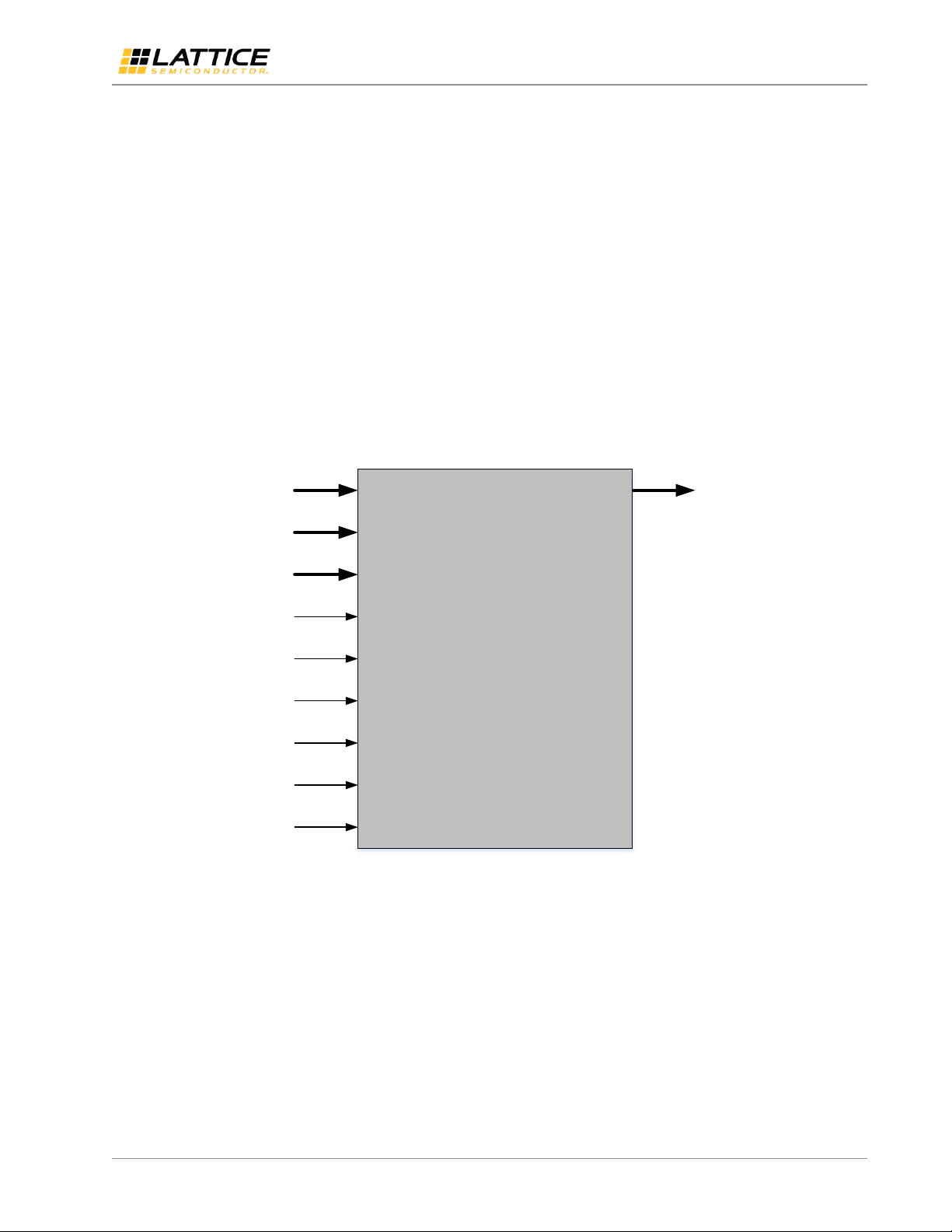
Each of the four 256 kb blocks of RAM is configured in 16K x 16 Single Port RAM. Figure 2.1 shows the block diagram of
the primitive for the 16K x 16 SPRAM block – SB_SPRAM256KA.
© 2016 Lattice Semiconductor Corp. All Lattice trademarks, registered trademarks, patents, and disclaimers are as listed at www.latticesemi.com/legal. All other brand or product names are
TN1314-1.0 3
Figure 2.1. SB_SPRAM256KA SPRAM Primitive
trademarks or registered trademarks of their respective holders. The specifications and information herein are subject to change without notice.
Page 4
iCE40 SPRAM Usage Guide
User
Primitive
Port Name
Test
Primitive
Port
Name
Primitive
Port
Width
HW
Port
Name
HW
Port
Width
Pin Name
Default Value
Description
Note
ADDRESS
—
[13:0]
ADR
[13:0]
Address
Input
14b’00000000000000
This Address Input
port is used to address
the location to be
written during the
write cycle and read
during the read cycle.
—
DATAIN
—
[15:0]
D
[15:0]
Data
Input
16b’0000000000000000
The Data Input bus is
used to write the data
into the memory
location specified by
Address input port
during the write cycle.
—
MASKWREN
—
[3:0]
WEM
[15:0]
Maskable
Write
Enable
4b’1111
It includes the Bit
Write feature where
selective write to
individual I/Os can be
done using the
Maskable Write
Enable signals. When
the memory is in write
cycle, one can write
selectively on some
I/Os.
1, 2
WREN
—
[0:0]
WE
[0:0]
Write
Enable
Input
1b’0
When the Write
Enable input is Logic
High, the memory is in
the write cycle.
When the Write
Enable is Logic Low,
the memory is in the
read cycle.
—
CHIPSELECT
—
[0:0]
ME
[0:0]
Memory
enable
input
1b’0
When the memory
enable input is Logic
High, the memory is
enabled and
read/write operations
can be performed.
When memory enable
input is logic Low, the
memory is
deactivated.
—
CLOCK
—
[0:0]
CLK
[0:0]
Clock
Input
—
This is the external
clock for the memory.
—
STANDBY
—
[0:0]
LS
[0:0]
Light
Sleep
Input
1b’0
When this pin is active
then memory goes
into low leakage
mode, there is no
change in the output
state.
3
Technical Note
2.2. SPRAM Port Definitions and GUI Options
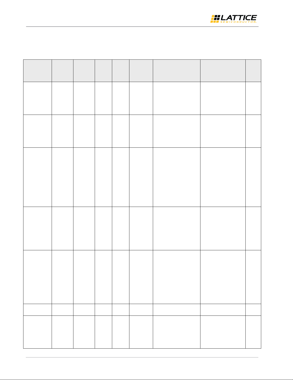
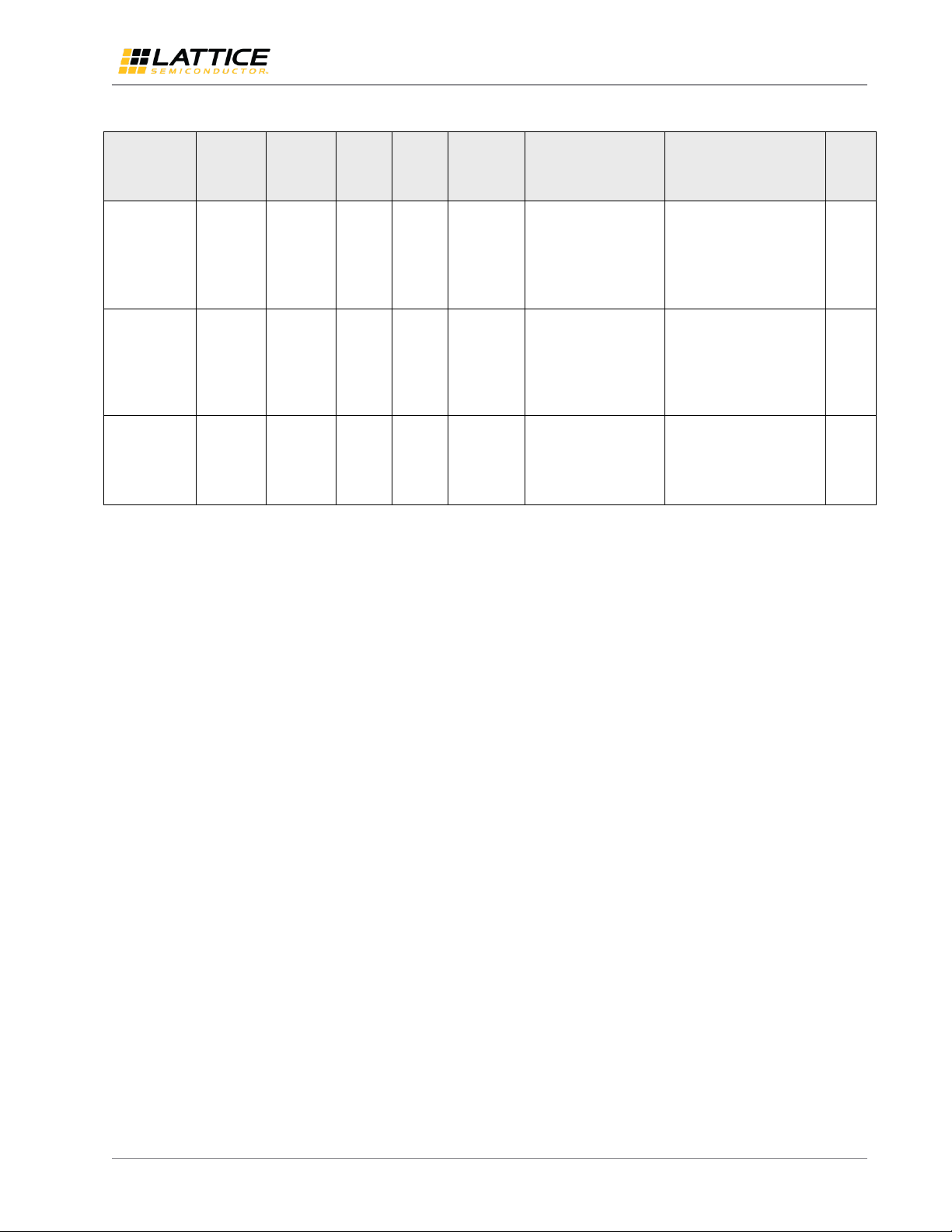
Table 2.1 shows the port definitions and the GUI options for the SPRAM.
Table 2.1. SB_SPRAM256KA RAM Port Definitions
© 2016 Lattice Semiconductor Corp. All Lattice trademarks, registered trademarks, patents, and disclaimers are as listed at www.latticesemi.com/legal. All other brand or product names are
4 TN1314-1.0
trademarks or registered trademarks of their respective holders. The specifications and information herein are subject to change without notice.
Page 5
iCE40 SPRAM Usage Guide
User
Primitive
Port Name
Test
Primitive
Port
Name
Primitive
Port
Width
HW
Port
Name
HW
Port
Width
Pin Name
Default Value
Description
Note
SLEEP
—
[0:0]
DS
[0:0]
Deep
Sleep
Input
1b’0
This pin shuts down
power to periphery and
maintains memory
contents.
The outputs of the
memory are pulled low.
3
POWEROFF
—
[0:0] — [0:0]
Power Off
Input
1b’1
This pin turns off the
power to the memory
core. Note that there is
no memory data
retention when this is
driven low.
4
DATAOUT
—
[15:0]
Q
[15:0]
Data
Output
bus
—
This pin outputs the
contents of the memory
location addressed by
the address Input
signals.
—
Technical Note
Table 2.1. SB_SPRAM256KA RAM Port Definitions (Continued)
Notes:
1. MASKWREN includes the nibble write masks for the DATAIN.
2. The default value of each MASKWREN is 1. In order to mask a nibble of DATAIN, the MASKWREN needs to be pulled low (0).
3. STANDBY, SLEEP signals are mutually exclusive. Refer to the Logic Truth Table (Power Modes) section in the datasheet for valid
4. POWEROFF is a signal that controls the built in power switch in each memory block. This signal when driven low (1’b0), shuts
There are no special attributes needed for SB_SPRAM256KA because it has fixed configuration of 16,384 addresses and
16 data width, running in Normal mode. The inputs (ADDRESS and DATAIN) are always registered. DATAOUT has no
registers.
SB_SPRAM256KA RAM does not support initialization through device configuration.
© 2016 Lattice Semiconductor Corp. All Lattice trademarks, registered trademarks, patents, and disclaimers are as listed at www.latticesemi.com/legal. All other brand or product names are
TN1314-1.0 5
The hardware port, WEM allows write mask for individual bits of DATAIN.
For external user primitive level, this mask is available for each nibble (4-bits). Thus the MASKWREN has to map to WEM as
follows:
MASKWREN(3) => WEM(15)
MASKWREN(3) => WEM(14)
MASKWREN(3) => WEM(13)
MASKWREN(3) => WEM(12)
MASKWREN(2) => WEM(11)
MASKWREN(2) => WEM(10)
MASKWREN(2) => WEM(9)
MASKWREN(2) => WEM(8)
MASKWREN(1) => WEM(7)
MASKWREN(1) => WEM(6)
MASKWREN(1) => WEM(5)
MASKWREN(1) => WEM(4)
MASKWREN(0) => WEM(3)
MASKWREN(0) => WEM(2)
MASKWREN(0) => WEM(1)
MASKWREN(0) => WEM(0)
The following shows which MASKWREN bits enable the mask for the DATAIN nibbles:
MASKWREN(3) enables mask for DATAIN(15:12)
MASKWREN(2) enables mask for DATAIN (11:8)
MASKWREN(1) enables mask for DATAIN (7:4)
MASKWREN(0) enables mask for DATAIN(3:0)
values for these signals in different states.
down the power to the memory. During the off state, there is no memory data retention.
When POWEROFF is driven high (1’b1), the SPRAM is powered on.
trademarks or registered trademarks of their respective holders. The specifications and information herein are subject to change without notice.
Page 6

iCE40 SPRAM Usage Guide
Technical Note
Power Save States for SPRAM 3.
The iCE40 provides a capability to place the SPRAM in a different power state, when not in use. There are three user
signals that control the power states of the RAM.
3.1. Normal State
Normal State is the normal operation of the memory. During this state, all three of the power save signals (STANDBY,
SLEEP and SHUTDOWN) are being driven Low. This is also the higher power consumption state of the SPRAM.
3.2. Standby State
Standby State is achieved when the STANDBY signal is driven High. When active, the memory goes in a low leakage
mode. The state of the outputs does not change when the RAM is placed in Standby State.
It is to be noted that Standby State is referred to as “Light Sleep” state in the RAM datasheet. The name STANDBY has
been chosen to match and be consistent with the power states for the Lattice Power Management Unit (PMU).
3.3. Sleep State
Sleep State is achieved when the SLEEP signal is driven High. This signal shuts down the power to the periphery of the
memory and maintains the memory contents. The outputs in this case are all pulled Low.
Sleep State is referred to as “Deep Sleep” state in the RAM datasheet. The name SLEEP has been chosen to match and
be consistent with the power states for the Lattice Power Management Unit (PMU).
3.4. Power Off State
Each RAM block has a power switch associated with it, and that power switch controls the SD signal of the RAM. Users
will be interfacing through CIB to the Power Switch and that will power down the memory.
Shut Down or Power Off State is achieved when the POWEROFF signal is driven Low. This signal shuts down the power
to the periphery of the memory and the memory core. In this state, there is no data retention of the memory. The
outputs in this case are all pulled low.
© 2016 Lattice Semiconductor Corp. All Lattice trademarks, registered trademarks, patents, and disclaimers are as listed at www.latticesemi.com/legal. All other brand or product names are
6 TN1314-1.0
trademarks or registered trademarks of their respective holders. The specifications and information herein are subject to change without notice.
Page 7

iCE40 SPRAM Usage Guide
Technical Note
Use Cases for User Primitive SB_SPRAM256KA 4.
This section describes the use cases of the SB_SPRAM256KA RAM blocks while instantiating, inferring, and cascading
these blocks.
4.1. Instantiating Memories
SB_SPRAM256KA primitive can be directly instantiated using both Verilog and VHDL at the top level. An example of
instantiating SB_SPRAM256KA RAM using Verilog:
// spram256 user modules //
SB_SPRAM256KA ramfn_inst1(
.DATAIN(DATAIN),
.ADDRESS(ADDRESS),
.MASKWREN(MASKWREN),
.WREN(WREN),
.CHIPSELECT(CHIPSELECT),
.CLOCK(CLOCK),
.STANDBY(STANDBY),
.SLEEP(SLEEP),
.POWEROFF(POWEROFF),
.DATAOUT(DATAOUT_A)
)
SB_SPRAM256KA ramfn_inst2(
.DATAIN(DATAIN),
.ADDRESS(ADDRESS),
.MASKWREN(MASKWREN),
.WREN(WREN),
.CHIPSELECT(CHIPSELECT),
.CLOCK(CLOCK),
.STANDBY(STANDBY),
.SLEEP(SLEEP),
.POWEROFF(POWEROFF),
.DATAOUT(DATAOUT_B)
)
4.2. Inferring Memories
The memory also supports memory inferring where a behavioral code for the SPRAM is synthesized in iCEcube2 to
create the RAM using the RAM primitives of ICE40 device. In order to use SB_SPRAM256KA RAM blocks, users can use
syn_ramstyle attribute.
The power save states (Standby, Sleep, and Power Off States) are not available when inferring the RAM. When
implementing the inferred RAM using SB_SPRAM256KA primitives, software should tie off the STANDBY, SLEEP and
SHUTDOWN ports to “0”. If power save features are desired, then users should use the method of instantiation and
connect these ports as per design requirements.
4.3. Output Pipeline Registers
The SB_SPRAM256KA does not include output registers.
When desired, pipeline registers are required to be implemented in the fabric. While inferring the RAM, the software
should implement the output pipeline registers in the fabric.
© 2016 Lattice Semiconductor Corp. All Lattice trademarks, registered trademarks, patents, and disclaimers are as listed at www.latticesemi.com/legal. All other brand or product names are
TN1314-1.0 7
trademarks or registered trademarks of their respective holders. The specifications and information herein are subject to change without notice.
Page 8
iCE40 SPRAM Usage Guide
Single Port RAM
Primitive
SB_SPRAM256KA
ADDRESS [13:0]
DATAIN [15:0]
WREN
MASKWREN [3:0]
CHIPSELECT
CLOCK
STANDBY
SLEEP
POWEROFF
DATAOUT [15:0]
Single Port RAM
Primitive
SB_SPRAM256KA
ADDRESS [13:0]
DATAIN [15:0]
WREN
MASKWREN [3:0]
CHIPSELECT
CLOCK
STANDBY
SLEEP
POWEROFF
DATAOUT [15:0]
1
0
1
0
DATAOUT [15 :0]
1
0
ADDRESS [14:0]
DATAIN [15:0]
WREN
MASKWREN [3:0]
CHIPSELECT
CLOCK
STANDBY
SLEEP
POWEROFF
ADDRESS [14]
ADDRESS [13:0]
Technical Note
4.4. Cascading Memories
Each SPRAM block is 256 kb, supporting configuration that are 16K x 16. These memories are cascaded to form larger
memory based on the user requirements. The memories can be cascaded in two ways:
Address Cascading or
Data Cascading.
The following sections provide examples of how each cascading type is achieved, and the connection of the signals
required. User can instantiate the RAM primitive and connect them using this as guidance to create larger memory
blocks.
Auto cascading is supported while inferring a RAM. Any additional logic required will be implemented in the device
fabric for creating larger memories.
Address Cascading (or Depth Cascading) 4.4.1.
Address/Depth cascading is useful when the memories are required to have the capacity of storing “more” words while
keeping the data width the same. In this case additional user logic is needed to decode the address.
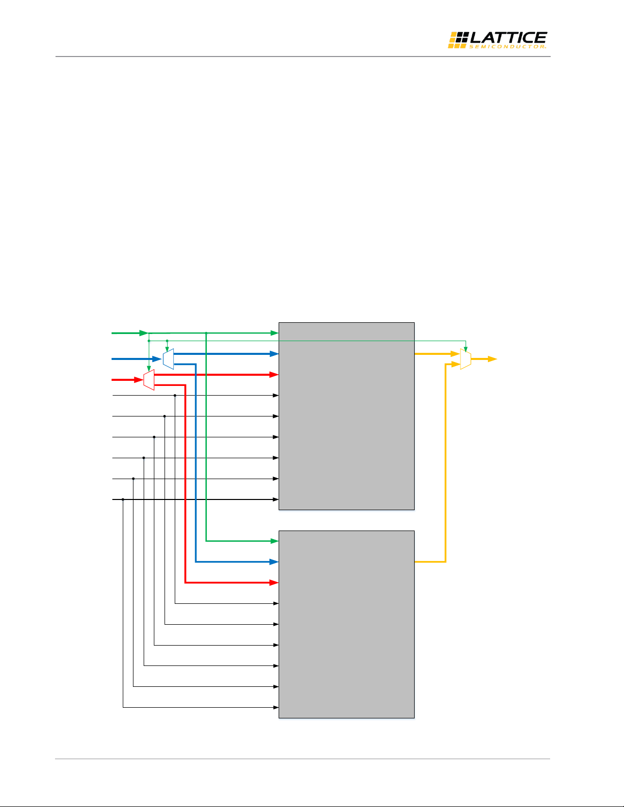
Figure 4.1 shows an example of the depth cascading of a 32K x 16 SPRAM. Additional logic is required that will guide
the data to the correct memory block using Muxes and Demuxes. The rest of the signals (that are not shown), should
be connected to both the memory blocks without any other logic requirements.
Figure 4.1. Address/Depth Cascading Example for 32K x 16 SPRAM using Primitive
© 2016 Lattice Semiconductor Corp. All Lattice trademarks, registered trademarks, patents, and disclaimers are as listed at www.latticesemi.com/legal. All other brand or product names are
8 TN1314-1.0
trademarks or registered trademarks of their respective holders. The specifications and information herein are subject to change without notice.
Page 9
iCE40 SPRAM Usage Guide
Single Port RAM
Primitive
SB_SPRAM256KA
ADDRESS [13:0]
DATAIN [15:0]
WREN
MASKWREN [3:0]
CHIPSELECT
CLOCK
STANDBY
SLEEP
POWEROFF
DATAOUT [15:0] DATAOUT [31:0]
ADDRESS [13:0]
DATAIN [31:0]
WREN
MASKWREN [7:0]
CHIPSELECT
CLOCK
STANDBY
SLEEP
POWEROFF
Single Port RAM
Primitive
SB_SPRAM256KA
ADDRESS [13:0]
DATAIN [15:0]
WREN
MASKWREN [3:0]
CHIPSELECT
CLOCK
STANDBY
SLEEP
POWEROFF
DATAOUT [15:0]
DATAIN [31:16]
MASKWREN [7:4]
DATAIN [15:0]
MASKWREN [3:0]
DATAOUT [31:16] DATAOUT [15:0]
Technical Note
Data Cascading (or Width Cascading)
4.4.2.
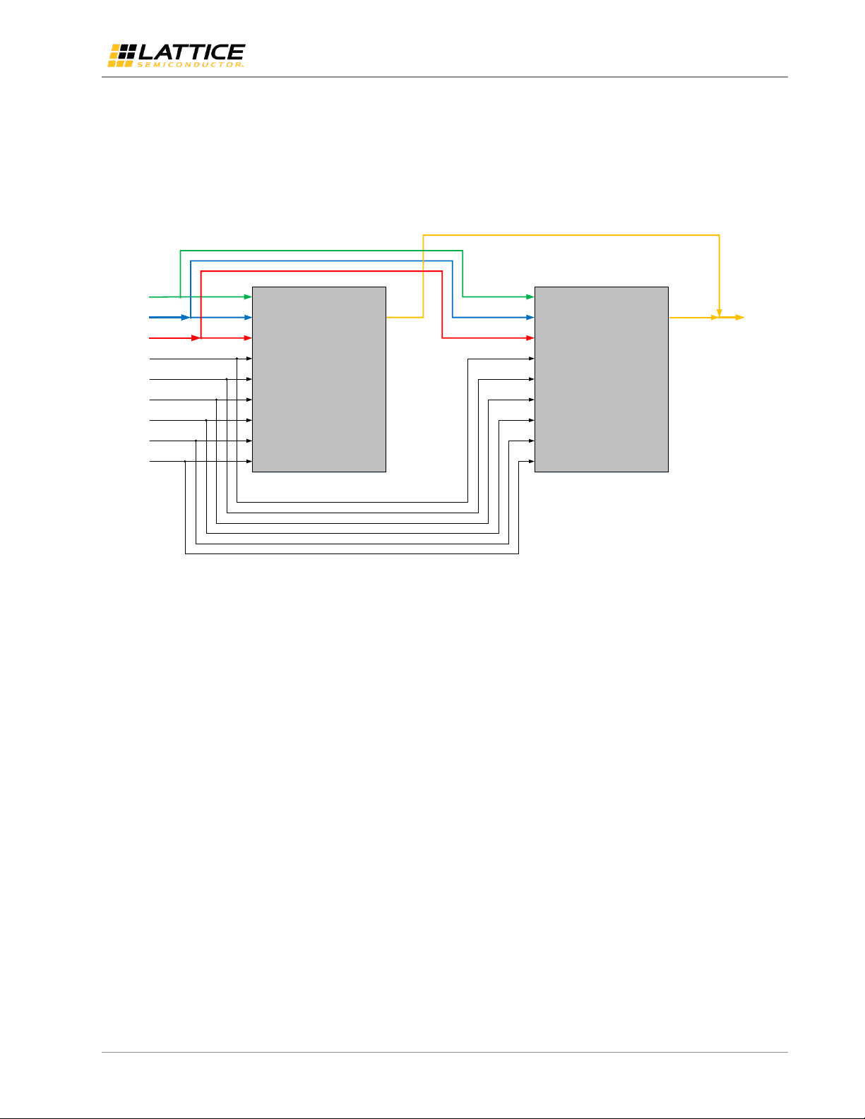
Data/Width cascading is useful when the memories are required to have the capacity of storing “longer” words while
keeping the address depth the same. In this case, very minimal user logic is needed, essentially for concatenating
words from individual SPRAM blocks.
Figure 4.2 shows an example of the Width cascading of a 16k x 32 SPRAM. The rest of the signals (that are not shown),
should be connected to both the memory blocks without any other logic requirements.
Figure 4.2. Data/Width Cascading Example for 16K x 32 SPRAM using Primitive
© 2016 Lattice Semiconductor Corp. All Lattice trademarks, registered trademarks, patents, and disclaimers are as listed at www.latticesemi.com/legal. All other brand or product names are
trademarks or registered trademarks of their respective holders. The specifications and information herein are subject to change without notice.
TN1314-1.0 9
Page 10

iCE40 SPRAM Usage Guide
Technical Note
Technical Support Assistance
Submit a technical support case through www.latticesemi.com/techsupport.
© 2016 Lattice Semiconductor Corp. All Lattice trademarks, registered trademarks, patents, and disclaimers are as listed at www.latticesemi.com/legal. All other brand or product names are
10 TN1314-1.0
trademarks or registered trademarks of their respective holders. The specifications and information herein are subject to change without notice.
Page 11

iCE40 SPRAM Usage Guide
Date
Version
Change Summary
June 2016
1.0
Initial release.
Technical Note
Revision History
© 2016 Lattice Semiconductor Corp. All Lattice trademarks, registered trademarks, patents, and disclaimers are as listed at www.latticesemi.com/legal. All other brand or product names are
TN1314-1.0 11
trademarks or registered trademarks of their respective holders. The specifications and information herein are subject to change without notice.
Page 12

7th Floor, 111 SW 5th Avenue
Portland, OR 97204, USA
T 503.268.8000
www.latticesemi.com
 Loading...