

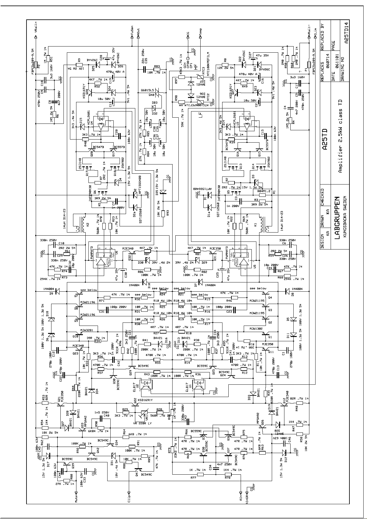
Page 1
Page 2

DESIGNATOR PARTNUMBER PARTNAME
-
- A25TD14b-Hxx A25TD14b-H03
C1 270p100VNP05%5 270p 100V
C2 10u50V 10u 50V
C3 1n200VNP05%5 1n 200V
C4 4n7250VMMK5 4n7 250V
C5 470n250VMMK15 470n 250V
C6 330n250VMMK15 330n 250V
C7 1n200VNP05%5 1n 200V
C8 4n7250VMMK5 4n7 250V
C9 470n250VMMK15 470n 250V
C10 330n250VMMK15 330n 250V
C11 10u50V 10u 50V
C12 270p100VNP05%5 270p 100V
C13 470p200VNP05%5 470p 200V
C14 3n3250VMMK5 3n3 250V
C15 100n63VMMK5 100n 63V
C16 470u40V10x30A 470u 40V A
C17 3u3160VMKP27.5B 3u3 160V
C18 3u3160VMKP27.5B 3u3 160V
C19 470u40V10x30A 470u 40V A
C20 100n63VMMK5 100n 63V
C21 3n3250VMMK5 3n3 250V
C22 470p200VNP05%5 470p 200V
C23 100p200VNP05%5 100p 200V
C24 10p200VNP05%5 10p 200V
C25 47u35V 47u 35V
C26 330n250VMMK15 330n 250V
C27 47u35V 47u 35V
C28 47u35V 47u 35V
C29 330n250VMMK15 330n 250V
C30 47u35V 47u 35V
C31 100p200VNP05%5 100p 200V
C32 10p200VNP05%5 10p 200V
C33 see below 100n63VMMK5
C34 4n7250VMMK5 4n7 250V
C35 22n250VMMK10 22n 250v
C36 33u50V 33u 50V
C37 33u50V 33u 50V
C38 33u50V 33u 50V
C39 33u50V 33u 50V
C40 1n5250VMMK5 1n5 250V
C41 1n200VNP05%5 1n 200V
C42 1n200VNP05%5 1n 200V
C43 330p200VNP05%5 330p200VNP05%5
C44 see below 100n63VMMK5
C45 see below 100n63VMMK5
C46 see below 100n63VMMK5
D3 15V1.3W5% 15V 1.3W 5%
D4 15V1.3W5% 15V 1.3W 5%
D5 100V1.3W5% 100V 1.3W 5%
Page 3

D6 100V1.3W5% 100V 1.3W 5%
D7 1N4004 1N4004
D8 1N4004 1N4004
D9 1N4004 1N4004
D10 1N4004 1N4004
D11 100V1.3W5% 100V 1.3W 5%
D12 15V1.3W5% 15V 1.3W 5%
D13 BAV21 BAV21
D14 3V3.4W5% 3V3 .4W 5%
D15 3V3.4W5% 3V3 .4W 5%
D16 BAV21 BAV21
D17 15V1.3W5% 15V 1.3W 5%
D18 100V1.3W5% 100V 1.3W 5%
D19 BYV26C BYV26C
D20 BAV21 BAV21
D21 BYV26C BYV26C
D22 BYV26C BYV26C
D23 9V1.4W5% 9V1 .4W 5%
D24 9V1.4W5% 9V1 .4W 5%
D25 BYV26C BYV26C
D26 BYV26C BYV26C
D27 BAV21 BAV21
D28 BYV26C BYV26C
D29 39V.4W2% 39V .4W 2%
D30 39V.4W2% 39V .4W 2%
D31 10V.4W5% 10V .4W 5%
D32 DB3 DB3
D33 BAV21 BAV21
D34 BAV21 BAV21
D35 15V1.3W5% 15V1.3W5%
D36 see below BAV21
D37 see below BAV21
K1 14uHD14-23 14uHD14-23
K2 14uHD14-23 14uHD14-23
P1 FBLPPC5x209M FBLPPC5x209M
P2 FBLPPC5x209M FBLPPC5x209M
P4 MH2x41ML MH2x41ML
Q13 2SJ148 2SJ148
Q14 2SK982 2SK982
Q15 BC559C BC559C
Q16 BC549C BC549C
Q17 2SJ148 2SJ148
Q18 2SK982 2SK982
Q19 BC559C BC559C
Q20 BC549C BC549C
Q24 BC549C BC549C
Q25 BC559C BC559C
Q26 MPSA92 MPSA92
Q27 KSD1691Y KSD1691Y
Q28 KSD1691Y KSD1691Y
Q29 BC549C BC549C
Q30 BC559C BC559C
Page 4

Q31 MJE350 MJE350
Q32 MJE340 MJE340
Q33 MPSA42 MPSA42
Q34 BC549C BC549C
Q35 BC559C BC559C
Q36 BC549C BC549C
Q37 BC549C BC549C
Q38 BC559C BC559C
Q39 BC559C BC559C
Q40 Q6015L5 Q6015L5
Q41 BC549C BC549C
Q42 BC549C BC549C
R1 R0.8 R0.8
R2 2R2.7W1% 2R2 .7W 1%
R3 3R92W5% 3R9 2W 5%
R4 1R52W5% 1R5 2W 5%
R5 3R92W5% 3R9 2W 5%
R6 1R52W5% 1R5 2W 5%
R7 2R2.7W1% 2R2 .7W 1%
R8 12K2W5% 12K 2W 5%
R9 12K2W5% 12K 2W 5%
R10 39R.7W1% 39R .7W 1%
R11 10K.7W1% 10K .7W 1%
R12 470R.7W1% 470R .7W 1%
R13 3K3.7W1% 3K3 .7W 1%
R14 470R.7W1% 470R .7W 1%
R15 Rxx variant dependent 10R.7W1%
R16 10R.7W1% 10R .7W 1%
R17 Rxx variant dependent 10R.7W1%
R18 4R7.7W1% 4R7 .7W 1%
R19 Rxx variant dependent R105W2% (5mm stand-off)
R20 R105W2% (5mm stand-off) R10 5W 2% (5mm stand-off)
R21 Rxx variant dependent R105W2% (5mm stand-off)
R22 10K.7W1% 10K .7W 1%
R23 10K.7W1% 10K .7W 1%
R24 Rxx variant dependent R105W2% (5mm stand-off)
R25 R105W2% (5mm stand-off) R10 5W 2% (5mm stand-off)
R26 Rxx variant dependent R105W2% (5mm stand-off)
R27 4R7.7W1% 4R7 .7W 1%
R28 536R.7W1% 536R .7W 1%
R29 3K3.7W1% 3K3 .7W 1%
R30 Rxx variant dependent 10R.7W1%
R31 10R.7W1% 10R .7W 1%
R32 Rxx variant dependent 10R.7W1%
R33 10K.7W1% 10K .7W 1%
R34 39R.7W1% 39R .7W 1%
R35 220R.7W1% 220R.7W1%
R36 100R.7W1% 100R .7W 1%
R37 180R.7W1% 180R .7W 1%
R38 200K.7W1% 200K .7W 1%
R39 3K3.7W1% 3K3 .7W 1%
R40 3K3.7W1% 3K3 .7W 1%
Page 5

R41 200K.7W1% 200K .7W 1%
R42 180R.7W1% 180R .7W 1%
R43 100R.7W1% 100R .7W 1%
R44 220R.7W1% 220R.7W1%
R45 1K.7W1% 1K.7W1%
R46 47K.7W1% 47K .7W 1%
R47 1K4.7W1% 1K4 .7W 1%
R48 82R.7W1% 82R .7W 1%
R49 4K7.7W1% 4K7 .7W 1%
R50 2M.7W1% 2M.7W1%
R51 1M.7W1% 1M .7W 1%
R52 4K7.7W1% 4K7 .7W 1%
R53 82R.7W1% 82R .7W 1%
R54 1K4.7W1% 1K4 .7W 1%
R55 470R.7W1% 470R .7W 1%
R56 3K3.7W1% 3K3 .7W 1%
R57 470R.7W1% 470R .7W 1%
R58 18K2W5% (5mm stand-off) 18K 2W 5% (5mm stand-off)
R59 2R22W5% 2R2 2W 5%
R60 2M.7W1% 2M.7W1%
R61 2R22W5% 2R2 2W 5%
R62 18K2W5% (5mm stand-off) 18K 2W 5% (5mm stand-off)
R63 6K8.7W1% 6K8 .7W 1%
R64 6K8.7W1% 6K8 .7W 1%
R65 47R.7W1% 47R .7W 1%
R66 47R.7W1% 47R .7W 1%
R67 47K.7W1% 47K .7W 1%
R68 294K.7W1% 294K .7W 1%
R69 560K.7W1% 560K.7W1%
R70 560K.7W1% 560K.7W1%
R71 47K.7W1% 47K .7W 1%
R73 294K.7W1% 294K .7W 1%
R74 47K.7W1% 47K .7W 1%
R75 47R.7W1% 47R .7W 1%
R76 47R.7W1% 47R .7W 1%
R77 1K.7W1% 1K .7W 1%
R78 1K4.7W1% 1K4 .7W 1%
R79 23K2.7W1% 23K2 .7W 1%
R80 27K.7W1% 27K .7W 1%
R81 4K7.7W1% 4K7.7W1%
R82 100K.7W1% 100K .7W 1%
R83 10R.7W1% 10R .7W 1%
R84 27K.7W1% 27K .7W 1%
R85 27K.7W1% 27K .7W 1%
R86 100K.7W1% 100K .7W 1%
R87 4K7.7W1% 4K7.7W1%
R88 10K.7W1% 10K .7W 1%
R89 47K.7W1% 47K .7W 1%
R90 6K04.7W1% 6K04 .7W 1%
R91 100K.7W1% 100K .7W 1%
R92 100K.7W1% 100K .7W 1%
R93 18K2W5% (5mm stand-off) 18K2W5% (5mm stand-off)
Page 6

R97 Rxx.7W1% 42K2.7W1%
R98 Rxx.7W1% 42K2.7W1%
U1 EL817 EL817
U2 EL817 EL817
U3 HCPL2601 HCPL2601
U4 HCPL2601 HCPL2601
VR1 VR220RLY2X3M VR 220R LY
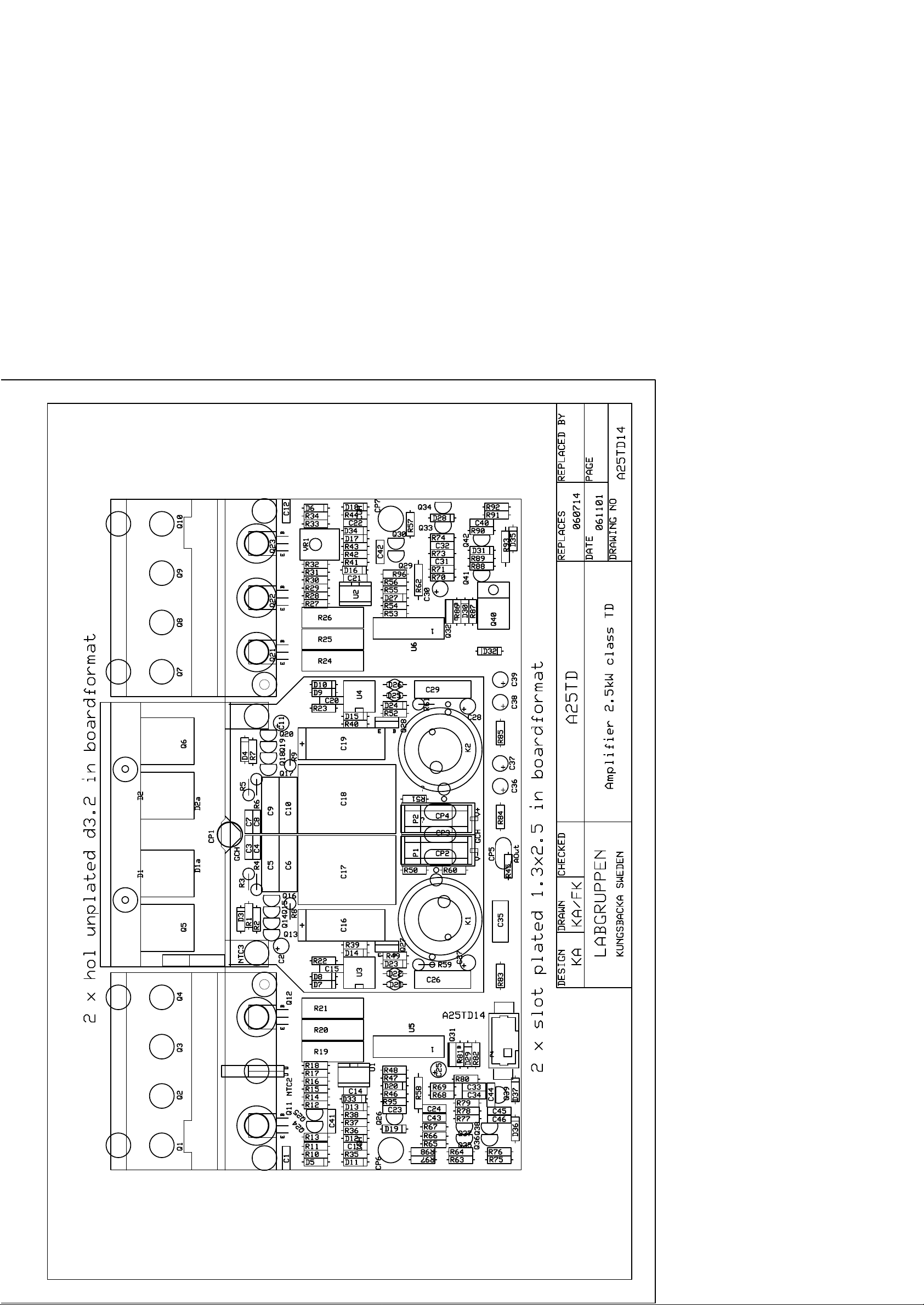
PCB A25TD14 A25TD14
A25TD14b-Mxx A25TD14b-M03
- A25TD14b-Hxx A25TD14b-H03
D1 STTH1506DPI STTH1506DPI
D2 STTH1506DPI STTH1506DPI
Q1 2SA1294 2SA1294
Q2 Qxx variant dependent 2SA1294
Q3 2SA1294 2SA1294
Q4 Qxx variant dependent 2SA1294
Q5 STY60NK30Z STY60NK30Z
Q6 STY60NK30Z STY60NK30Z
Q7 Qxx variant dependent 2SC3263
Q8 2SC3263 2SC3263
Q9 Qxx variant dependent 2SC3263
Q10 2SC3263 2SC3263
Q11 MJE350 MJE350
Q12 MJE340 MJE340
Q21 MJE350 MJE350
Q22 KSD1691Y KSD1691Y
Q23 MJE340 MJE340
NTC1 NTC100KPEFILM NTC100KPEFILM
NTC2 NTC100KPEFILM NTC100KPEFILM
see instruction FS15x4x1 FS15x4x1
see instruction RSI-2642 RSI-2642
see instruction CLJTNTC CLJTNTC
see instruction CLTO247x4 CLTO247x4
see instruction COCTO247X4TS COCTO247x4TS
see instruction COCTO247X4 COCTO247x4
see instruction COCTO247X4 COCTO247x4
see instruction MRT103x6 MRT103x6
see instruction MRT103x12 MRT103x12
see instruction BRB3.2x8x1 BRB3.2x8x1
see instruction FBB3.1 FBB3.1
see instruction M6MM3 M6MM3
see instruction T3x10_LAB T3x10_LAB
see instruction BRV3.2x8x.6 BRV3.2x8x.6
see instruction ISMI12.5x10d3.1 ISMI12.5x10d3.1
see instruction ISMI24x17.6 ISMI24x17.6
see instruction ISSR17x8 ISSR17x8
see instruction SA25TD14b-Mxx see instruction
U5 PWMNATD-F01 PWMNATD-F01
U6 PWMPATD-F01 PWMPATD-F01
Page 7

see instruction Fxx variant dependent
see instruction LSxx variant dependent
A25TD14b-FXX A25TD14b-F05
A25TD14b-MXX A25TD14b-M03
R21 Rxx variant dependent see below
R24 Rxx variant dependent see below
R95 RXX.7W1% 866R.7W1%
R96 RXX.7W1% 866R.7W1%
see instruction Fxx variant dependent
see instruction LSxx variant dependent
see instruction LSxx variant dependent SA25TD14b-F05
Page 8

OBJLAYER MOUNT BOMEXCLUDE
TOP NO
TOP NO
TOP NO
TOP NO
TOP NO
TOP NO
TOP NO
TOP NO
TOP NO
TOP NO
TOP NO
TOP NO
TOP NO
TOP NO
TOP NO
TOP NO
TOP NO
TOP NO
TOP NO
TOP NO
TOP NO
TOP NO
TOP NO
TOP NO
TOP NO
TOP NO
TOP NO
TOP NO
TOP NO
TOP NO
TOP NO
TOP NO
TOP NO
TOP NO
TOP NO
TOP NO
TOP NO
TOP NO
TOP NO
TOP NO
TOP NO
TOP NO
TOP NO
TOP NO
TOP NO
TOP NO
TOP NO
TOP NO
TOP NO
Page 9

TOP NO
TOP NO
TOP NO
TOP NO
TOP NO
TOP NO
TOP NO
TOP NO
TOP NO
TOP NO
TOP NO
TOP NO
TOP NO
TOP NO
TOP NO
TOP NO
TOP NO
TOP NO
TOP NO
TOP NO
TOP NO
TOP NO
TOP NO
TOP NO
TOP NO
TOP NO
TOP NO
TOP NO
TOP NO
TOP NO
TOP NO
TOP NO
TOP NO
TOP NO
TOP NO
TOP NO
TOP NO
TOP NO
TOP NO
TOP NO
TOP NO
TOP NO
TOP NO
TOP NO
TOP NO
TOP NO
TOP NO
TOP NO
TOP NO
TOP NO
TOP NO
TOP NO
Page 10

TOP NO
TOP NO
TOP NO
TOP NO
TOP NO
TOP NO
TOP NO
TOP NO
TOP NO
TOP NO
TOP NO
TOP NO
TOP NO
TOP NO
TOP NO
TOP NO
TOP NO
TOP NO
TOP NO
TOP NO
TOP NO
TOP NO
TOP NO
TOP NO
TOP NO
TOP NO
TOP NO
TOP NO
TOP NO
TOP NO
TOP NO
TOP NO
TOP NO
TOP NO
TOP NO
TOP NO
TOP NO
TOP NO
TOP NO
TOP NO
TOP NO
TOP NO
TOP NO
TOP NO
TOP NO
TOP NO
TOP NO
TOP NO
TOP NO
TOP NO
TOP NO
TOP NO
Page 11

TOP NO
TOP NO
TOP NO
TOP NO
TOP NO
TOP NO
TOP NO
TOP NO
TOP NO
TOP NO
TOP NO
TOP NO
TOP NO
TOP NO
TOP NO
TOP NO
TOP NO
TOP NO
TOP NO
TOP NO
TOP NO
TOP NO
TOP NO
TOP NO
TOP NO
TOP NO
TOP NO
TOP NO
TOP NO
TOP NO
TOP NO
TOP NO
TOP NO
TOP NO
TOP NO
TOP NO
TOP NO
TOP NO
TOP NO
TOP NO
TOP NO
TOP NO
TOP NO
TOP NO
TOP NO
TOP NO
TOP NO
TOP NO
TOP NO
TOP NO
TOP NO
TOP NO
Page 12

TOP NO
TOP NO
TOP NO
TOP NO
TOP NO
TOP NO
TOP NO
TOP NO
NO
see instruction NO
see instruction NO
see instruction NO
see instruction NO
see instruction NO
see instruction NO
see instruction NO
see instruction NO
see instruction NO
see instruction NO
see instruction NO
see instruction NO
see instruction NO
see instruction NO
see instruction NO
see instruction NO
see instruction NO
see instruction NO
see instruction NO
see instruction NO
see instruction NO
see instruction NO
see instruction NO
see instruction NO
see instruction NO
see instruction NO
see instruction NO
see instruction NO
see instruction NO
see instruction NO
see instruction NO
see instruction NO
see instruction NO
see instruction NO
see instruction NO
see instruction NO
see instruction NO
see instruction NO
see instruction NO
Page 13

see instruction NO
see instruction NO
NO
see instruction NO
see instruction NO
see instruction NO
see instruction NO
see instruction NO
see instruction NO
see instruction NO
Page 14

Page 15

Page 16

Page 17

Page 18

Page 19

Page 20
Page 21
Page 22
Page 23
Page 24
Page 25
Page 26

Page 27

Page 28

Page 29

Page 30

Page 31

Page 32

Page 33

Page 34

TP0610L/T, VP0610L/T, BS250
V
Continuous Drain Current
Vishay Siliconix
P-Channel 60-V (D-S) MOSFET
PRODUCT SUMMARY
Part Number V
TP0610L −60 10 @ VGS = −10 V −1 to −2.4 −0.18
TP0610T −60 10 @ VGS = −10 V −1 to −2.4 −0.12
VP0610L −60 10 @ VGS = −10 V −1 to −3.5 −0.18
VP0610T −60 10 @ VGS = −10 V −1 to −3.5 −0.12
BS250 −45 14 @ VGS = −10 V −1 to −3.5 −0.18
FEATURES BENEFITS APPLICATIONS
D High-Side Switching
D Low On-Resistance: 8 W
D Low Threshold: −1.9 V
D Fast Switching Speed: 16 ns
D Low Input Capacitance: 15 pF
(BR)DSS
Min (V)
r
Max (W)
DS(on)
D Ease in Driving Switches
D Low Offset (Error) Voltage
D Low-Voltage Operation
D High-Speed Switching
D Easily Driven Without Buffer
V
(V) ID (A)
GS(th)
D Drivers: Relays, Solenoids, Lamps,
Hammers, Displays, Memories,
Transistors, etc.
D Battery Operated Systems
D Power Supply, Converter Circuits
D Motor Control
TO-92-18RM
(TO-18 Lead Form)
D
G
S
1
2
3
Top View
BS250TP0610L
Device Marking
Front View
BS250
“S” BS
250
xxll
“S” = Siliconix Logo
xxll = Date Code
TO-236
(SOT-23)
G
1
S
2
Top View
TP0610T
VP0610T
S
G
D
TO-226AA
(TO-92)
1
2
3
Top View
VP0610L
Device Marking
Device Marking
Front View
Front View
TP0610L
“S” TP
0610L
xxll
VP0610L
“S” VP
0610L
xxll
“S” = Siliconix Logo
xxll = Date Code
ABSOLUTE MAXIMUM RATINGS (TA = 25_C UNLESS OTHERWISE NOTED)
Parameter Symbol TP0610L TP0610T VP0610L VP0610T BS250 Unit
Drain-Source Voltage V
Gate-Source Voltage V
Continuous Drain Current
(TJ = 150_C)
Pulsed Drain Current
Power Dissipation
Thermal Resistance, Junction-to-Ambient R
Operating Junction and Storage Temperature Range TJ, T
Notes
a. Pulse width limited by maximum junction temperature.
For applications information see AN804.
a
TA= 25_C
TA= 100_C
TA= 25_C
TA= 100_C
I
I
DM
P
thJA
DS
GS
D
D
stg
−60 −60 −60 −60 −45
"30 "30 "30 "30 "25
−0.18 −0.12 −0.18 −0.12 −0.18
−0.11 −0.07 −0.11 −0.07
−0.8 −0.4 −0.8 −0.4
0.8 0.36 0.8 0.36 0.83
0.32 0.14 0.32 0.14
156 350 156 350 150
−55 to 150
Marking Code:
D
3
TP0610T: TOwll
VP0610T: VOwll
w = Week Code
lL = Lot Traceability
A
W
_C/W
_C
Document Number: 70209
S-41260—Rev. H, 05-Jul-04
www.vishay.com
1
Page 35

TP0610L/T, VP0610L/T, BS250
Drain Source
V
V
yg
GSS
Drain Current
DSS
m
Current
b
D(on)
Drain-Source
Forward
pF
VDD = 25 V, RL = 133 W
Vishay Siliconix
SPECIFICATIONS (TA = 25_C UNLESS OTHERWISE NOTED)
Parameter Symbol Test Conditions
Static
Typ
Limits
TP0610L/T VP0610L/T BS250
a
Min Max Min Max Min Max Unit
Drain-Source
Breakdown Voltage
Gate-Threshold
Voltage
Gate-Body Leakage I
Zero Gate Voltage
Drain Current
On-State Drain
b
Current
Drain-Source
On-Resistance
Forward
Transconductance
Diode Forward
Voltage
b
b
Dynamic
(BR)DSS
V
GS(th)
GSS
I
DSS
I
D(on)
r
DS(on)
g
fs
V
SD
VGS = 0 V, ID = −10 mA
VGS = 0 V, ID = −100 mA
VDS = VGS, ID = −1 mA −1.9 −1 −2.4 −1 −3.5 −1 −3.5
VDS = 0 V, VGS = "20 V "10 "10
VDS = 0 V, VGS = "20 V, TJ = 125_C
VDS = 0 V, VGS = "15 V "20
VDS = −48 V, VGS = 0 V −1 −1
VDS = −48 V, VGS = 0 V, TJ = 125_C
VDS = −25 V, VGS = 0 V −0.5
VDS = −10 V, VGS = −4.5 V −180 −50
VDS = −10 V, VGS = −10 V
VGS = −4.5 V, ID = −25 mA 11 25
VGS = −10 V, ID = −0.5 A L Suffix 8 10 10
VGS = −10 V, ID = −0.5 A, TJ = 125_C
VGS = −10 V, ID = −0.2 A T Suffix 6.5 10 10 14
VDS = −10 V, ID = −0.5 A L Suffix 20 80
VDS = −10 V, ID = −0.1 A T Suffix 90 60 70
IS = −0.5 A, VGS = 0 V −1.1 V
L Suffix −750 −600
T Suffix −220
L Suffix 15 20 20
−70 −60 −60
"50
−200 −200
−45
V
nA
mA
mA
W
mS
Input Capacitance C
Output Capacitance C
Reverse Transfer
Capacitance
Switching
Turn-On Time t
Turn-Off Time t
Notes
a. For DESIGN AID ONLY, not subject to production testing. VPDS06
b. Pulse test: PW v300 ms duty cycle v2%.
c. Switching time is essentially independent of operating temperature.
www.vishay.com
c
C
oss
rss
ON
OFF
iss
VDS = −25 V, VGS = 0 V
f = 1 MHz
VDD = −25 V, RL = 133 W
ID ^ −0.18 A, V
= −10 V, Rg = 25 W
GEN
2
15 60 60
10 25 25
3 5 5
8 10
8 10
Document Number: 70209
S-41260—Rev. H, 05-Jul-04
pF
ns
Page 36

TP0610L/T, VP0610L/T, BS250
TYPICAL CHARACTERISTICS (25_C UNLESS NOTED)
Vishay Siliconix
Output Characteristics Transfer Characteristics
1.0
VGS = 10 V
0.8
0.6
0.4
− Drain Current (A)I
D
0.2
0.0
012345
8 V
VDS − Drain-to-Source Voltage (V)
7 V
6 V
5 V
4 V
On-Resistance vs. Drain Current
20
16
W )
12
VGS = 4.5 V
VGS = 5 V
1200
TJ = −55_C
900
600
− Drain Current (mA)I
D
300
0
0246810
− Gate-to-Source Voltage (V)
V
GS
GS
= 0 V
Capacitance
40
V
32
24
125_C
C
iss
25_C
8
− On-Resistance (r
DS(on)
4
0
0 200 400 600 800 1000
ID − Drain Current (mA)
15
ID = 500 mA
12
9
6
− Gate-to-Source Voltage (V)
GS
3
V
0
0.0 0.3 0.6 0.9 1.2 1.5 1.8
Gate Charge
VDS = 30 V
Qg − Total Gate Charge (nC)
VGS = 10 V
VDS = 48 V
16
C − Capacitance (pF)
8
0
0 5 10 15 20 25
1.8
1.5
1.2
0.9
0.6
− On-Resiistance
(Normalized)
DS(on)
r
0.3
0.0
−50 −25 0 25 50 75 100 125 150
C
oss
C
rss
VDS − Drain-to-Source Voltage (V)
On-Resistance vs. Junction Temperature
VGS = 10 V @ 500 mA
VGS = 4.5 V @ 25 mA
TJ − Junction Temperature (_C)
Document Number: 70209
S-41260—Rev. H, 05-Jul-04
www.vishay.com
3
Page 37

TP0610L/T, VP0610L/T, BS250
Vishay Siliconix
TYPICAL CHARACTERISTICS (25_C UNLESS NOTED)
1000
VGS = 0 V
100
TJ = 125_C
10
− Source Current (A)I
S
TJ = 25_C
TJ = −55_C
1
0.00 0.3 0.6 0.9
VSD − Source-to-Drain Voltage (V)
Threshold Voltage Variance Over Temperature
0.5
Source-Drain Diode Forward Voltage
0.4
0.3
0.2
Variance (V)V
0.1
−0.0
GS(th)
−0.1
−0.2
ID = 250 mA
1.2 1.5
On-Resistance vs. Gate-Source Voltage
10
8
ID = 500 mA
W )
6
4
− On-Resistance (r
ID = 200 mA
2
DS(on)
0
0246810
VGS − Gate-to-Source Voltage (V)
Single Pulse Power, Junction-to-Ambient
3
2.5
2
1.5
Power (W)
1
0.5
TA = 25_C
−0.3
−50 −25 0 25 50 75 100 125 150
0.1
Thermal Impedance
Normalized Effective Transient
0.01
www.vishay.com
4
2
1
Duty Cycle = 0.5
0.2
0.1
0.05
0.02
−4
10
T
− Junction Temperature (_C)
J
Normalized Thermal Transient Impedance, Junction-to-Ambient
Single Pulse
−3
10
0
0.01
1
10
100 6000.1
Time (sec)
Notes:
P
DM
t
1
t
2
t
thJA
t
thJA
100
1
2
(t)
= 350_C/W
1. Duty Cycle, D =
2. Per Unit Base = R
3. TJM − TA = PDMZ
4. Surface Mounted
−2
10
−1
1 10 60010
Square Wave Pulse Duration (sec)
Document Number: 70209
S-41260—Rev. H, 05-Jul-04
Page 38

Legal Disclaimer Notice
Vishay
Disclaimer
All product specifications and data are subject to change without notice.
Vishay Intertechnology, Inc., its affiliates, agents, and employees, and all persons acting on its or their behalf
(collectively, “Vishay”), disclaim any and all liability for any errors, inaccuracies or incompleteness contained herein
or in any other disclosure relating to any product.
Vishay disclaims any and all liability arising out of the use or application of any product described herein or of any
information provided herein to the maximum extent permitted by law. The product specifications do not expand or
otherwise modify Vishay’s terms and conditions of purchase, including but not limited to the warranty expressed
therein, which apply to these products.
No license, express or implied, by estoppel or otherwise, to any intellectual property rights is granted by this
document or by any conduct of Vishay.
The products shown herein are not designed for use in medical, life-saving, or life-sustaining applications unless
otherwise expressly indicated. Customers using or selling Vishay products not expressly indicated for use in such
applications do so entirely at their own risk and agree to fully indemnify Vishay for any damages arising or resulting
from such use or sale. Please contact authorized Vishay personnel to obtain written terms and conditions regarding
products designed for such applications.
Product names and markings noted herein may be trademarks of their respective owners.
Document Number: 91000 www.vishay.com
Revision: 18-Jul-08 1
Page 39

Checklist after service of class
TD Mark II
C 16:4, C 28:4, C 48:4, C 68:4, C 88:4,
Modified: 2009-11-04
Page 1 of 12
FP 4000, FP 6000Q, FP 7000, FP 9000, FP 10000Q, FP 13000 & FP 14000
Created by: Patrick Bergwall
Date: 2007-04-23
THIS DOCUMENT IS CONFIDENTIAL. IT MAY NOT BE REPRODUCED WITHOUT THE WRITTEN PERMISSION OF Lab.gruppen AB
2006 Lab.gruppen AB, Faktorvägen 1, S-434 44 KUNGSBACKA, SWEDEN
Page 40

Modified: 2009-11-04
Page 2 of 12
Index
1 INTRODUCTION............................................................................................................ 3
2 CHECK LIST CLASS TD MARK II............................................................................. 3
THIS DOCUMENT IS CONFIDENTIAL. IT MAY NOT BE REPRODUCED WITHOUT THE WRITTEN PERMISSION OF Lab.gruppen AB
2006 Lab.gruppen AB, Faktorvägen 1, S-434 44 KUNGSBACKA, SWEDEN
Page 41

Modified: 2009-11-04
Page 3 of 12
1 Introduction
This checklist shall be used to make sure the amplifier is always checked in a proper way after
service has been done. It is important to follow the steps in this check list and check all points
so that the set up of parameters in the amplifier is correct adjusted. When have done all
checks and adjusted the parameters the amplifier will work properly and will have the output
power that it is designed for.
2 Check list class TD Mark II
Always clean the amplifier by blowing with compressed air through coolers and fans. Be
careful when blowing where big electrolytic capacitors are placed so that the capacitor doesn’t
get damaged.
THIS DOCUMENT IS CONFIDENTIAL. IT MAY NOT BE REPRODUCED WITHOUT THE WRITTEN PERMISSION OF Lab.gruppen AB
2006 Lab.gruppen AB, Faktorvägen 1, S-434 44 KUNGSBACKA, SWEDEN
Page 42

Modified: 2009-11-04
Page 4 of 12
1) After repair always start the amplifier with current potentiometer (VR1) located on
PWMF1-board. On is clockwise (cw) and off is counter clockwise (ccw). Check that the
switch pulse is normal. 300V line should increase some volts when relay clicks.
1.
Connect an oscilloscope probe.
Measuring points (old layout). Measuring points (new layout).
2.
VR1 fully ccw.
VR1
VR1-PWMF1
THIS DOCUMENT IS CONFIDENTIAL. IT MAY NOT BE REPRODUCED WITHOUT THE WRITTEN PERMISSION OF Lab.gruppen AB
2006 Lab.gruppen AB, Faktorvägen 1, S-434 44 KUNGSBACKA, SWEDEN
Page 43

Modified: 2009-11-04
3.
Insert mains plug into variac.
4.
Mains switch ON and remote switch MANUAL
Page 5 of 12
5.
Slowly turn variac up, at the same time look at power-
supply oscilloscope.
6.
Begin turning VR1 cw.
Waveform should look like below picture.
230VAC
THIS DOCUMENT IS CONFIDENTIAL. IT MAY NOT BE REPRODUCED WITHOUT THE WRITTEN PERMISSION OF Lab.gruppen AB
2006 Lab.gruppen AB, Faktorvägen 1, S-434 44 KUNGSBACKA, SWEDEN
Page 44

7.
At a certain point, power supply will regulate.
Then, turn current potentiometer fully cw.
Modified: 2009-11-04
120-140V +/- RAIL
Page 6 of 12
8.
Power supply frequency decreases, PAL led goes out.
23kHz 43µS
THIS DOCUMENT IS CONFIDENTIAL. IT MAY NOT BE REPRODUCED WITHOUT THE WRITTEN PERMISSION OF Lab.gruppen AB
2006 Lab.gruppen AB, Faktorvägen 1, S-434 44 KUNGSBACKA, SWEDEN
Page 45

Modified: 2009-11-04
Page 7 of 12
Step 9, 10
Only for C 16:4, C 28:4, C 48:4, C 68:4, C 88:4, FP 4000, FP 6000Q, FP 7000
& FP 10000Q.
9.
Begin turning voltage adjust potentiometer.
ca +/- 174V
At 174V (+/- 2V) power supply will stop.
10.
Adjust voltage.
+/- 160V
VR1-SP100F/
VR1-SP130F
VR1-SP100F/
VR1-SP130F
Adjustment point
Measuring points
THIS DOCUMENT IS CONFIDENTIAL. IT MAY NOT BE REPRODUCED WITHOUT THE WRITTEN PERMISSION OF Lab.gruppen AB
2006 Lab.gruppen AB, Faktorvägen 1, S-434 44 KUNGSBACKA, SWEDEN
Page 46

Step 11, 12
Only for FP 9000, FP 13000 & FP 14000.
11.
Begin turning voltage adjust potentiometer.
At 220V (+/- 2V) power supply will stop.
12.
Adjust voltage.
Modified: 2009-11-04
ca +/- 220V
+/- 200V
Page 8 of 12
VR1-SP130F
VR1-SP130F
Adjustment point
Measuring points
THIS DOCUMENT IS CONFIDENTIAL. IT MAY NOT BE REPRODUCED WITHOUT THE WRITTEN PERMISSION OF Lab.gruppen AB
2006 Lab.gruppen AB, Faktorvägen 1, S-434 44 KUNGSBACKA, SWEDEN
Page 47

Modified: 2009-11-04
Page 9 of 12
Step 13
Only for C 16:4, C 28:4, C 48:4, C 68:4, C 88:4, FP 4000, FP 6000Q, FP 7000
& FP 10000Q.
13.
Measure voltages according to chart:
1 GND -
2 ca 2V Trafotemp
3 +25V 15VUnr
4 GND -
5 +58V 50VUnr
6 -18V 50VUNrR
7 +15V Pwrgood
8 +5V PAL
Step 14
Only for FP 9000, FP 13000 & FP 14000.
14.
Measure voltages according to chart:
1 GND -
2 ca 2V Trafotemp
3 +22-23V 15VUnr
4 GND -
5 +52-53V 50VUnr
6 -18V 50VUNrR
7 +15V Pwrgood
8 +5V PAL
THIS DOCUMENT IS CONFIDENTIAL. IT MAY NOT BE REPRODUCED WITHOUT THE WRITTEN PERMISSION OF Lab.gruppen AB
2006 Lab.gruppen AB, Faktorvägen 1, S-434 44 KUNGSBACKA, SWEDEN
Page 48

15.
Following tests are made for all Channels, check offset with
Modified: 2009-11-04
no input +/- 40mV.
Following tests are made for all Channels, check offset with
no input and no load +/- 2V.
Increase input signal and check output signal at clip 8Ω
Wave measured at 1.3kHz. Wave measured at 13kHz.
Page 10 of 12
THIS DOCUMENT IS CONFIDENTIAL. IT MAY NOT BE REPRODUCED WITHOUT THE WRITTEN PERMISSION OF Lab.gruppen AB
2006 Lab.gruppen AB, Faktorvägen 1, S-434 44 KUNGSBACKA, SWEDEN
Page 49

16.
Check HF-wave at 1.3kHz and 13kHz at 8Ω.
4 channel amplifier 2 channel amplifier
Modified: 2009-11-04
No input signal
No input signal
Page 11 of 12
Clip 1.3 kHz.
Clip 13 kHz.
THIS DOCUMENT IS CONFIDENTIAL. IT MAY NOT BE REPRODUCED WITHOUT THE WRITTEN PERMISSION OF Lab.gruppen AB
2006 Lab.gruppen AB, Faktorvägen 1, S-434 44 KUNGSBACKA, SWEDEN
Page 50

17.
Power supply frequency increases when loaded.
18.
Short capacitors according to pictures (Ch A=C1,
Ch B=C101, Ch C=C201, Ch D=C301).
Fans will increase speed, TEMP leds on front will light,
Signal will go out.
4 Channels
Modified: 2009-11-04
40kHz
AICO
Page 12 of 12
2 Channels
19) Check mains switch for bad contact (click noise).
20) Check gain potentiometers at front. No disturbance at output signal shall be detected when
turning the potentiometer from one end point to the other end point.
21) Check dust filter, change when needed.
THIS DOCUMENT IS CONFIDENTIAL. IT MAY NOT BE REPRODUCED WITHOUT THE WRITTEN PERMISSION OF Lab.gruppen AB
2006 Lab.gruppen AB, Faktorvägen 1, S-434 44 KUNGSBACKA, SWEDEN
Page 51

File: ‘L:\Production\Service\Service Bulletin\Service Bulletin 2008 no 2 A25TD14b.doc
Document type:
SERVICE BULLETIN
Created:
(2008-03-19) Page 1 of 3
Technical Service Bulletin
Created by: Lab.gruppen AB Service Department
Date: 080319
Reference no: A25TD14b
Affected models
Following models are affected by this technical service bulletin:
C68:4
C48:4
C28:4
C16:4
Page:
Affected boards/modules
A25TD14b, AICO410d, AICO410e.
Symptom
A25TD14b does not fit together with AICO410d. If changing A25TD module to A25TD14b
AICO410d must be rebuilt to an AICO410e. See table below for modifications on AICO410d
to be rebuilt to an AICO410e.
THIS DOCUMENT IS CONFIDENTIAL. IT MAY NOT BE REPRODUCED WITHOUT THE WRITTEN PERMISSION OF LABGRUPPEN AB AND TC Electronic A/S
2005 Labgruppen AB, Faktorvägen 1, S-434 44 KUNGSBACKA, SWEDEN |.
Page 52

File: ‘L:\Production\Service\Service Bulletin\Service Bulletin 2008 no 2 A25TD14b.doc
Document type:
SERVICE BULLETIN
Created:
(2008-03-19) Page 2 of 3
Page:
Solution
See table below for modifications on AICO410d to be rebuilt to an AICO410e. Exchange
resistors according to table below to rebuild the AICO410d to AICO410e.
Explanation to the resistors value: 24K.125W1%0805 equals a SMD resistor (0805) with the
value of 24kΩ, 0.125W and 1% accuracy.
Position Value on component on
AICO410d
R1 24K.125W1%0805 100K.125W1%0805
R101 24K.125W1%0805 100K.125W1%0805
R201 24K.125W1%0805 100K.125W1%0805
R301 24K.125W1%0805 100K.125W1%0805
Value on component on
AICO410e
R2 120K.125W1%0805 270K.125W1%0805
R102 120K.125W1%0805 270K.125W1%0805
R202 120K.125W1%0805 270K.125W1%0805
R302 120K.125W1%0805 270K.125W1%0805
R96 0R.125W1%0805 330K.125W1%0805
R196 0R.125W1%0805 330K.125W1%0805
R296 0R.125W1%0805 330K.125W1%0805
R396 0R.125W1%0805 330K.125W1%0805
It is common SMD resistors that shall be used. Those might be purchased at a local dealer.
Note
It is different A25TD modules for different amplifiers.
Part numbers
Model Part numbers
C68:4 A25TD14b, AICO410d, AICO410e, also see table above
C48:4 A25TD14b, AICO410d, AICO410e, also see table above
C28:4 A25TD14b, AICO410d, AICO410e, also see table above
C16:4 A25TD14b, AICO410d, AICO410e, also see table above
THIS DOCUMENT IS CONFIDENTIAL. IT MAY NOT BE REPRODUCED WITHOUT THE WRITTEN PERMISSION OF LABGRUPPEN AB AND TC Electronic A/S
2005 Labgruppen AB, Faktorvägen 1, S-434 44 KUNGSBACKA, SWEDEN |.
Page 53

File: ‘L:\Production\Service\Service Bulletin\Service Bulletin 2008 no 2 A25TD14b.doc
Document type:
SERVICE BULLETIN
Created:
(2008-03-19) Page 3 of 3
History
Date Created By Status Bulletin no. Comment
080319 JF SHARP 2
Page:
THIS DOCUMENT IS CONFIDENTIAL. IT MAY NOT BE REPRODUCED WITHOUT THE WRITTEN PERMISSION OF LABGRUPPEN AB AND TC Electronic A/S
2005 Labgruppen AB, Faktorvägen 1, S-434 44 KUNGSBACKA, SWEDEN |.
Page 54

Document type:
SERVICE BULLETIN
Created:
(2010-06-28) Page 1
Page:
Technical Service Bulletin No. 16
Created by: Lab.gruppen AB Service Department
Date: 100628
Reference no: Unstable rail voltage, not able to adjust rail voltage.
Affected models
Following models are affected by this technical service bulletin:
C:16, C:28, C:48, C:68 & C:88.
FP 4000, FP 6000Q, FP 7000, FP 9000, FP 10000Q, FP 13000 & FP 14000.
Affected boards/modules
SP100, SP130 and SP140.
Symptom
Unstable rail voltage, not able to adjust rail voltage.
PSU clicking on and off all the time and PAL led lights up.
Solution
1. Check if there is contact between + rail and R32 & R34.
2. Check if there is contact between – rail and R33.
3. If not repair foil pattern and check D23, D24, D25, D26, D27, Q8, Q9 & Q10.
4. Update OVP circuit if needed, regarding to instruction (Only SP100 & SP130).
History
Date Created By Status Bulletin no. Comment
100628 PB Sharp 16
THIS DOCUMENT IS CONFIDENTIAL. IT MAY NOT BE REPRODUCED WITHOUT THE WRITTEN PERMISSION OF LAB.GRUPPEN AB AND TC Electronic A/S
2005 Lab.gruppen AB, Faktorvägen 1, S-434 44 KUNGSBACKA, SWEDEN |.
Page 55

Lab Part No.
Description
Amount
Info
Pos
6n8250VMMK5
Wima: FKS2 6800PF 10% 400VDC
1
C12
6n8250VMMK5
Epcos: B32529-C3682-K289
1
C12
Document type: Created: Page:
SERVICE BULLETIN (2011-10-11) Page 1 of 2
Technical Service Bulletin No. 27
Created by: Lab.gruppen AB Service Department
Date: 2011-10-11
Reference no: C12
It is highly recommended to implement this service bulletin as preventative maintenance if the
unit is serviced for another issue.
Affected models
FP+.
C16:4, C28:4, C48:4, C68:4, C88:4.
PLM10000Q, PLM14000.
Affected boards/modules
SP100FXXx-FXX
SP130FXXx-FXX
SP140F01a-FXX, SP140F01b-FXX
Symptom
Screaming sound from power supply if amplifier powers up.
Amplifier does not power up.
Solution
Replace capacitor C12 with either of below listed components.
THIS DOCUMENT IS CONFIDENTIAL. IT MAY NOT BE REPRODUCED WITHOUT THE WRITTEN PERMISSION OF LAB.GRUPPEN AB AND TC Electronic A/S
2005 Lab.gruppen AB, Faktorvägen 1, S-434 44 KUNGSBACKA, SWEDEN |.
Page 56

Date
Created By
Status
Bulletin no.
Comment
2011-10-11
CL
SHARP
27
C12
Document type: Created: Page:
SERVICE BULLETIN (2011-10-11) Page 2 of 2
Service Log Information
Write “Technical Service Bulletin no.27” in column “Repair Remedy” besides other normal
repair information.
History
THIS DOCUMENT IS CONFIDENTIAL. IT MAY NOT BE REPRODUCED WITHOUT THE WRITTEN PERMISSION OF LAB.GRUPPEN AB AND TC Electronic A/S
2005 Lab.gruppen AB, Faktorvägen 1, S-434 44 KUNGSBACKA, SWEDEN |.
Page 57

Page 58

Page 59

Page 60

Senast ändrad: see filename
DESIGNATOR PARTNUMBER PARTNAME OBJLAYER MOUNT
Smallest denominator Hole mounting
C1 Cxx variant dependent see below TOP
C2 22n1000VMKP22.5 22n 1000V TOP
C3 470p500VY5P5%5 470p 500V TOP
C4 - see below TOP
C5 2200u200V35x55 2200u 200V TOP
C6 2200u200V35x55 2200u 200V TOP
C7 - see below TOP
C8 22n1000VMKP22.5 22n 1000V TOP
C9 10u50V 10u 50V TOP
C10 1n200VNP05%5 1n 200V TOP
C11 150p500VK20005%5 150p 500V TOP
C12 6n8250VMMK5 6n8 250V TOP
C13 100u50V 100u 50V TOP
C14 100u50V 100u 50V TOP
C15 1n5250VY1Y5P10 1n5250VY1Y5P10 TOP
C16 220p2000VB310%5 see below TOP
C17 68u100VLZ 68u 100VLZ TOP
C18 680u35VLZ 680u 35V LZ TOP
C19 1n200VNP05%5 1n 200V TOP
C20 1n200VNP05%5 1n 200V TOP
C21 100n63VMMK5 100n 63V TOP
C22 100n63VMMK5 100n 63V TOP
C23 100n63VMMK5 100n 63V TOP
C24 100n63VMMK5 100n 63V TOP
C25 10n250VMMK5 10n 250V TOP
C26 10u50V 10u 50V TOP
C27 4n71000VMKP15 4n7 1000V TOP
C28 4n71000VMKP15 4n7 1000V TOP
C29 Cxx variant dependent see below TOP
C30 2200u160V35x45 see below TOP
C31 2200u160V35x45 see below TOP
C32 Cxx variant dependent see below TOP
C33 Cxx variant dependent see below TOP
C34 Cxx variant dependent see below TOP
C35 Cxx variant dependent see below TOP
C36 Cxx variant dependent see below TOP
C37 Cxx variant dependent see below TOP
C38 Cxx variant dependent see below TOP
C39 Cxx variant dependent see below TOP
C40 Cxx variant dependent see below TOP
C41 1n200VNP05%5 1n 200V TOP
D2 BYM26E BYM26E TOP
D4 15V1.3W5% 15V 1.3W 5% TOP
D5 BYM26E BYM26E TOP
D7 1N4004 1N4004 TOP
D8 BYV26C BYV26C TOP
D9 BYV26C BYV26C TOP
Page 61

D10 BYV26C BYV26C TOP
D11 BYW98-200 BYW98-200 TOP
D12 BYW98-200 BYW98-200 TOP
D13 1N4148 1N4148 TOP
D16 12V.4W5% 12V .4W 5% TOP
D17 1N4148 1N4148 TOP
D18 39V.4W2% 39V .4W 2% TOP
D19 12V.4W5% 12V .4W 5% TOP
D20 5V6.4W2% 5V6.4W2% TOP
D21 1N4148 1N4148 TOP
D22 1N4148 1N4148 TOP
D23 39V.4W2% 39V .4W 2% TOP
D24 5V6.4W2% 5V6.4W2% TOP
L1 400uHETD29ST 400uH ETD29GSP TOP
L2 47uHA 47uH TOP
P1 TPC90M3 TPC90M3 TOP
P2 FBPC5x209M PC5X20 TOP
P3 FBPC5x209M PC5X20 TOP
P4 TPC90M3 TPC90M3 TOP
Q4 BC327 BC327 TOP
Q5 BC549C BC549C TOP
Q6 PN4392 PN4392 TOP
Q7 BC559C BC559C TOP
Q8 MPSA42 MPSA42 TOP
Q9 BC549C BC549C TOP
Q10 MPSA92 MPSA92 TOP
Q11 BC559C BC559C TOP
R1 1K3W5% (5mm stand-off) 1K3W5% (5mm stand-off) TOP
R2 2R2.7W1% 2R2.7W1% TOP
R3 2R2.7W1% 2R2.7W1% TOP
R4 2R2.7W1% 2R2.7W1% TOP
R5 100R.7W1% 100R .7W 1% TOP
R6 R105W2% (5mm stand-off) R10 5W 2% (5mm stand-off) TOP
R7 R105W2% (5mm stand-off) R10 5W 2% (5mm stand-off) TOP
R8 Rxx variant dependent see below TOP
R9 Rxx variant dependent see below TOP
R10 Rxx variant dependent see below TOP
R11 Rxx variant dependent see below TOP
R12 - see below TOP
R13 - see below TOP
R14 100K3W5% (5mm stand-off) 100K 3W 5% (5mm stand-off) TOP
R15 6M2.7W1% 6M2 .7W 1% TOP
R16 3M9.7W1% 3M9 .7W 1% TOP
R17 100K3W5% (5mm stand-off) 100K 3W 5% (5mm stand-off) TOP
R18 330R2W5% (5mm stand-off) 330R 2W 5% (5mm stand-off) TOP
R19 33R2W5% (5mm stand-off) 33R2W5% (5mm stand-off) TOP
R20 2R22W5% 2R2 2W 5% TOP
R21 2R22W5% 2R2 2W 5% TOP
R22 100R.7W1% 100R .7W 1% TOP
R23 470K.7W1% 470K .7W 1% TOP
R24 470K.7W1% 470K .7W 1% TOP
R25 47K.7W1% 47K .7W 1% TOP
Page 62

R26 180K.7W1% 180K.7W1% TOP
R27 47K.7W1% 47K .7W 1% TOP
R28 56K.7W1% see below TOP
R29 390K.7W1% 390K .7W 1% TOP
R30 6K8.7W1% 6K8 .7W 1% TOP
R31 10K.7W1% 10K.7W1% TOP
R32 330K.7W1% see below TOP
R33 10K.7W1% 10K .7W 1% TOP
R34 100K3W5% (5mm stand-off) see below TOP
R35 180K.7W1% 180K.7W1% TOP
R36 47K.7W1% 47K .7W 1% TOP
R37 56K.7W1% 56K .7W 1% TOP
R38 1M.7W1% 1M.7W1% TOP
R39 100K.7W1% 100K.7W1% TOP
R40 2M2.7W1% 2M2.7W1% TOP
R41 330K.7W1% 330K.7W1% TOP
U2 TCET1102G TCET1102G TOP
U3 TCET1102G TCET1102G TOP
U4 TCET1102G TCET1102G TOP
VR1 VR4K7LY2X3M VR 4K7 LY TOP
BOARD SP100F SP100F TOP
Smallest Denomination Final assembly
- SP100F-H02 Hole mounted board
see instruction SSP100F-M02 part no. Label see instruction
CL1 COATO247x2 COATO247x2 see instruction
CL2 COAEXTO247x5 COAEXTO247x5 see instruction
CP20 AWG18RED300VVW1 à 28 cm see instruction
CP21 AWG18RED300VVW1 à 46 cm see instruction
CP22 AWG18RED300VVW1 à 28 cm see instruction
CP23 AWG18RED300VVW1 à 46 cm see instruction
CP24 AWG20BLK300VVW1 à 28 cm see instruction
CP25 AWG20BLK300VVW1 à 46 cm see instruction
CP26 AWG20BLK300VVW1 à 28 cm see instruction
CP27 AWG20BLK300VVW1 à 46 cm see instruction
CP30 AWG18BLU300VVW1 à 28 cm see instruction
CP31 AWG18BLU300VVW1 à 46 cm see instruction
CP32 AWG18BLU300VVW1 à 28 cm see instruction
CP33 AWG18BLU300VVW1 à 46 cm see instruction
D1 GBPC35-06WL GBPC35-06WL see instruction
D14 STTA3006PI STTA3006PI see instruction
D15 STTA3006PI STTA3006PI see instruction
D3 BYT30PI1000 BYT30PI1000 see instruction
D6 STTA1512PI STTA1512PI see instruction
Q1 Qxx variant dependent see below see instruction
Q2 SGW25N120 SGW25N120 see instruction
Q3 Qxx variant dependent see below see instruction
see instruction COADB1 COADB1 see instruction
see instruction MRT204x20 MRT204x20 see instruction
see instruction M6MM4 M6MM4 see instruction
see instruction FBB4.1SV FBB4.1SV see instruction
Page 63

see instruction RTK10ST2.9x9.5 RTK10ST2.9x9.5 see instruction
see instruction MRTGF3x8FBBBRBSV MRTGF3x8FBBBRBSV see instruction
see instruction MRT103x12 MRT103x12 see instruction
see instruction FBB3.1 FBB3.1 see instruction
see instruction BRB3.2x6x.5SV BRB3.2x6x.5SV see instruction
see instruction CT98x2.5 CT98x2.5 see instruction
see instruction T3A15250-5x20 see below see instruction
see instruction ST3A15AL250-5x20 see below see instruction
U1 PWMF1-F01 PWMF1 see instruction
Mounted at Lab.gruppen
SUBxxx SP100F-M02
LSxxx SSP100F-F02
R13 5K36.7W1% see below TOP
LSxxx K1 T2K5WF160VPM8770 see below see instruction
C4 2200uF200V35x45
C7 2200uF200V35x45
C33 2200uF160V35x45
C34 2200uF160V35x45
see instruction FPMSA FPMSA see instruction
see instruction MPPM8770 MPPM8770 see instruction
see instruction M6MM4 M6MM4 see instruction
see instruction FBB1.4SV FBB1.4SV see instruction
see instruction CLCFPM8770 CLCFPM8770 see instruction
see instruction TPT8-2.5x10 TPT8-2.5x10 see instruction
see instruction FBB2.6 FBB2.6 see instruction
see instruction MRT104x80 special om Torx see instruction
Page 64

BOMEXCLUDE
NO
NO
NO
NO
NO
NO
NO
NO
NO
NO
NO
NO
NO
NO
NO
NO
NO
NO
NO
NO
NO
NO
NO
NO
NO
NO
NO
NO
NO
NO
NO
NO
NO
NO
NO
NO
NO
NO
NO
NO
NO
NO
NO
NO
NO
NO
NO
Page 65

NO
NO
NO
NO
NO
NO
NO
NO
NO
NO
NO
NO
NO
NO
NO
NO
NO
NO
NO
NO
NO
NO
NO
NO
NO
NO
NO
NO
NO
NO
NO
NO
NO
NO
NO
NO
NO
NO
NO
NO
NO
NO
NO
NO
NO
NO
NO
NO
NO
NO
NO
NO
Page 66

NO
NO
NO
NO
NO
NO
NO
NO
NO
NO
NO
NO
NO
NO
NO
NO
NO
NO
NO
NO
NO
NO
NO
NO
NO
NO
NO
NO
NO
NO
NO
NO
NO
NO
NO
NO
NO
NO
NO
NO
NO
NO
NO
NO
NO
NO
NO
NO
NO
Page 67

NO
NO
NO
NO
NO
NO
NO
NO
NO
NO
NO
NO
NO
NO
NO
NO
NO
NO
NO
Page 68

Page 69

Page 70

Page 71

Page 72

Senast ändrad: see filename
DESIGNATOR PARTNUMBER PARTNAME OBJLAYER MOUNT
Smallest denominator Hole mounting
C1 22n1000VMKP22.5 see below TOP
C2 22n1000VMKP22.5 22n 1000V TOP
C3 470p500VY5P5%5 470p 500V TOP
C4 2200u200V35x45 see below TOP
C5 2200u200V35x55 2200u 200V TOP
C6 2200u200V35x55 2200u 200V TOP
C7 2200u200V35x45 see below TOP
C8 22n1000VMKP22.5 22n 1000V TOP
C9 10u50V 10u 50V TOP
C10 1n200VNP05%5 1n 200V TOP
C11 150p500VK20005%5 150p 500V TOP
C12 6n8250VMMK5 6n8 250V TOP
C13 100u50V 100u 50V TOP
C14 100u50V 100u 50V TOP
C15 1n5250VY1Y5P10 1n5250VY1Y5P10 TOP
C16 220p2000VB310%5 see below TOP
C17 68u100VLZ 68u 100VLZ TOP
C18 680u35VLZ 680u 35V LZ TOP
C19 1n200VNP05%5 1n 200V TOP
C20 1n200VNP05%5 1n 200V TOP
C21 100n63VMMK5 100n 63V TOP
C22 100n63VMMK5 100n 63V TOP
C23 100n63VMMK5 100n 63V TOP
C24 100n63VMMK5 100n 63V TOP
C25 10n250VMMK5 10n 250V TOP
C26 10u50V 10u 50V TOP
C27 4n71000VMKP15 4n7 1000V TOP
C28 4n71000VMKP15 4n7 1000V TOP
C29 Cxx variant dependent see below TOP
C30 2200u160V35x45 see below TOP
C31 2200u160V35x45 see below TOP
C32 Cxx variant dependent see below TOP
C33 2200u160V35x45 see below TOP
C34 2200u160V35x45 see below TOP
C35 Cxx variant dependent see below TOP
C36 2200u160V35x45 see below TOP
C37 2200u160V35x45 see below TOP
C38 Cxx variant dependent see below TOP
C39 Cxx variant dependent see below TOP
C40 Cxx variant dependent see below TOP
C41 1n200VNP05%5 1n 200V TOP
D2 BYM26E BYM26E TOP
D4 15V1.3W5% 15V 1.3W 5% TOP
D5 BYM26E BYM26E TOP
D7 1N4004 1N4004 TOP
D8 BYV26C BYV26C TOP
D9 BYV26C BYV26C TOP
Page 73

D10 BYV26C BYV26C TOP
D11 BYW98-200 BYW98-200 TOP
D12 BYW98-200 BYW98-200 TOP
D13 1N4148 1N4148 TOP
D16 12V.4W5% 12V .4W 5% TOP
D17 1N4148 1N4148 TOP
D18 39V.4W2% 39V .4W 2% TOP
D19 12V.4W5% 12V .4W 5% TOP
D20 5V6.4W2% 5V6.4W2% TOP
D21 1N4148 1N4148 TOP
D22 1N4148 1N4148 TOP
D23 39V.4W2% 39V .4W 2% TOP
D24 5V6.4W2% 5V6.4W2% TOP
L1 400uHETD29ST 400uH ETD29GSP TOP
L2 47uHA 47uH TOP
P1 TPC90M3 TPC90M3 TOP
P2 FBPC5x209M PC5X20 TOP
P3 FBPC5x209M PC5X20 TOP
P4 TPC90M3 TPC90M3 TOP
Q4 BC327 BC327 TOP
Q5 BC549C BC549C TOP
Q6 PN4392 PN4392 TOP
Q7 BC559C BC559C TOP
Q8 MPSA42 MPSA42 TOP
Q9 BC549C BC549C TOP
Q10 MPSA92 MPSA92 TOP
Q11 BC559C BC559C TOP
R1 1K3W5% (5mm stand-off) 1K3W5% (5mm stand-off) TOP
R2 2R2.7W1% 2R2.7W1% TOP
R3 2R2.7W1% 2R2.7W1% TOP
R4 2R2.7W1% 2R2.7W1% TOP
R5 100R.7W1% 100R .7W 1% TOP
R6 R105W2% (5mm stand-off) R10 5W 2% (5mm stand-off) TOP
R7 R105W2% (5mm stand-off) R10 5W 2% (5mm stand-off) TOP
R8 R105W2% (5mm stand-off) see below TOP
R9 R105W2% (5mm stand-off) see below TOP
R10 Rxx variant dependent see below TOP
R11 Rxx variant dependent see below TOP
R12 - see below TOP
R13 2K7.7W1% see below TOP
R14 100K3W5% (5mm stand-off) 100K 3W 5% (5mm stand-off) TOP
R15 6M2.7W1% 6M2 .7W 1% TOP
R16 3M9.7W1% 3M9 .7W 1% TOP
R17 100K3W5% (5mm stand-off) 100K 3W 5% (5mm stand-off) TOP
R18 330R2W5% (5mm stand-off) 330R 2W 5% (5mm stand-off) TOP
R19 33R2W5% (5mm stand-off) 33R2W5% (5mm stand-off) TOP
R20 2R22W5% 2R2 2W 5% TOP
R21 2R22W5% 2R2 2W 5% TOP
R22 100R.7W1% 100R .7W 1% TOP
R23 470K.7W1% 470K .7W 1% TOP
R24 470K.7W1% 470K .7W 1% TOP
R25 47K.7W1% 47K .7W 1% TOP
Page 74

R26 180K.7W1% 180K.7W1% TOP
R27 47K.7W1% 47K .7W 1% TOP
R28 56K.7W1% see below TOP
R29 390K.7W1% 390K .7W 1% TOP
R30 6K8.7W1% 6K8 .7W 1% TOP
R31 10K.7W1% 10K.7W1% TOP
R32 330K.7W1% see below TOP
R33 10K.7W1% 10K .7W 1% TOP
R34 100K3W5% (5mm stand-off) see below TOP
R35 180K.7W1% 180K.7W1% TOP
R36 47K.7W1% 47K .7W 1% TOP
R37 56K.7W1% 56K .7W 1% TOP
R38 1M.7W1% 1M.7W1% TOP
R39 100K.7W1% 100K.7W1% TOP
R40 2M2.7W1% 2M2.7W1% TOP
R41 330K.7W1% 330K.7W1% TOP
U2 TCET1102G TCET1102G TOP
U3 TCET1102G TCET1102G TOP
U4 TCET1102G TCET1102G TOP
VR1 VR4K7LY2X3M VR 4K7 LY TOP
BOARD SP100F SP100F TOP
Smallest Denomination Final assembly
- SP100F-H03 Hole mounted board
see instruction SSP100F-F03 part no. Label see instruction
CL1 COATO247x2 COATO247x2 see instruction
CL2 COAEXTO247x5 COAEXTO247x5 see instruction
CP20 AWG18RED300VVW1 à 28 cm see instruction
CP21 AWG18RED300VVW1 à 46 cm see instruction
CP22 AWG18RED300VVW1 à 28 cm see instruction
CP23 AWG18RED300VVW1 à 46 cm see instruction
CP24 AWG20BLK300VVW1 à 28 cm see instruction
CP25 AWG20BLK300VVW1 à 46 cm see instruction
CP26 AWG20BLK300VVW1 à 28 cm see instruction
CP27 AWG20BLK300VVW1 à 46 cm see instruction
CP30 AWG18BLU300VVW1 à 28 cm see instruction
CP31 AWG18BLU300VVW1 à 46 cm see instruction
CP32 AWG18BLU300VVW1 à 28 cm see instruction
CP33 AWG18BLU300VVW1 à 46 cm see instruction
D1 GBPC35-06WL GBPC35-06WL see instruction
D14 STTA3006PI STTA3006PI see instruction
D15 STTA3006PI STTA3006PI see instruction
D3 BYT30PI1000 BYT30PI1000 see instruction
D6 STTA1512PI STTA1512PI see instruction
Q1 SGW25N120 see below see instruction
Q2 SGW25N120 SGW25N120 see instruction
Q3 Qxx variant dependent see below see instruction
see instruction COADB1 COADB1 see instruction
see instruction MRT204x20 MRT204x20 see instruction
see instruction M6MM4 M6MM4 see instruction
see instruction FBB4.1SV FBB4.1SV see instruction
Page 75

see instruction RTK10ST2.9x9.5 RTK10ST2.9x9.5 see instruction
see instruction MRTGF3x8FBBBRBSV MRTGF3x8FBBBRBSV see instruction
see instruction MRT103x12 MRT103x12 see instruction
see instruction FBB3.1 FBB3.1 see instruction
see instruction BRB3.2x6x.5SV BRB3.2x6x.5SV see instruction
see instruction CT98x2.5 CT98x2.5 see instruction
see instruction T3A15250-5x20 see below see instruction
see instruction ST3A15AL250-5x20 see below see instruction
U1 PWMF1-F01 PWMF1 see instruction
Mounted at Lab.gruppen
SUBxxx SP100F-F03
LSxxx R13 - see below TOP
LSxxx LSxx variant dependent
K1 T5KWF160VPM8770 see below see instruction
C4 Cxx Variant dependent
C7 Cxx Variant dependent
C33 Cxx Variant dependent
C34 Cxx Variant dependent
see instruction FPMSA FPMSA see instruction
see instruction MPPM8770 MPPM8770 see instruction
see instruction M6MM4 M6MM4 see instruction
see instruction FBB1.4SV FBB1.4SV see instruction
see instruction CLCFPM8770 CLCFPM8770 see instruction
see instruction TPT8-2.5x10 TPT8-2.5x10 see instruction
see instruction FBB2.6 FBB2.6 see instruction
see instruction MRT104x80 special om Torx see instruction
Page 76

BOMEXCLUDE
NO
NO
NO
NO
NO
NO
NO
NO
NO
NO
NO
NO
NO
NO
NO
NO
NO
NO
NO
NO
NO
NO
NO
NO
NO
NO
NO
NO
NO
NO
NO
NO
NO
NO
NO
NO
NO
NO
NO
NO
NO
NO
NO
NO
NO
NO
NO
Page 77

NO
NO
NO
NO
NO
NO
NO
NO
NO
NO
NO
NO
NO
NO
NO
NO
NO
NO
NO
NO
NO
NO
NO
NO
NO
NO
NO
NO
NO
NO
NO
NO
NO
NO
NO
NO
NO
NO
NO
NO
NO
NO
NO
NO
NO
NO
NO
NO
NO
NO
NO
NO
Page 78

NO
NO
NO
NO
NO
NO
NO
NO
NO
NO
NO
NO
NO
NO
NO
NO
NO
NO
NO
NO
NO
NO
NO
NO
NO
NO
NO
NO
NO
NO
NO
NO
NO
NO
NO
NO
NO
NO
NO
NO
NO
NO
NO
NO
NO
NO
NO
NO
NO
Page 79

NO
NO
NO
NO
NO
NO
NO
NO
NO
NO
NO
NO
NO
NO
NO
NO
NO
NO
NO
Page 80

Page 81

Page 82

Page 83

 Loading...