

Page 1

VSBC-32
Combined VMEbus System Controller and
Serial Communications Controller Board
Manual ID 21168, Rev. Index 04
Jul 00
The product described in this manual is
in compliance with all ap plied CE standards.
Page 2
General VSBC-32
Revision History
Manual/Product Title: VSBC-32
Manual ID Number: 21168
Rev.
Index
0100 Initial Issue 00/1 Aug 95
0200 General corrections 00/2 D ec 95
0201 J9 default setting chan ged 00/2 Nov 96
0300 General corrections and new manual structure 01 Dec 96
0301 New Preface 01 Aug 98
0311 Improvement to Fig. 2.1.3. In Appendices, correc-
04 Information of Er rata S heets 0100 _1/2 in tegra ted,
Brief Description of Ch anges Board Index
01 Sept 98
tions to flash a ddres ses on pag es MEM-2 to
MEM-4, page MEM-5 replaced.
01 Ju ly 00
adequate manual structure , new mem ory piggybacks mentioned, desc riptio n of co mbi ned sys tem
and communications con troller fuc ntionality,
function-related board diagrams, cohere nt terminology (e.g. proce ssor and bo ard varia nt names)
etc. Appendices mod ified, upda ted, reduced .
Date of
Issue
Imprint
Copyright © 2000 PEP Modular Computers GmbH. All rights
reserved. This manual may not be c opied, photocopied, reproduced, translated or converted to any electronic or machinereadable form in whole or in part without prior written approval of
PEP Modular Computers GmbH.
Disclaimer:
PEP Modular Computers GmbH rejects any liability for the cor-
rectnesss and completeness of this manual as well as its suitability for any part icular purpo se.
This manual was realized by: TPD/Engineering, PEP Modular Computers GmbH.
ID 21168, Rev. 04Page ii © 2000 PEP Modular Computers GmbH
Page 3

VSBC-32 Contents
Contents
Preface
Preface ..................................................................................................................... ix
Proprietary Note ....................................................................................................... ix
Trademarks .............................................................................................................. ix
Explanation of Symbols ..................... .... ..... .............................................................. x
For Your Safety ........................................................................................................ xi
High Voltage Safety Instructions .............................................................................. xi
Special Handling and Unpacking Instructions .......................................................... xi
General Instructions on Usage ............................................................................... xii
Two Year Warranty ................................................................................................ xiii
Chapt
Chapter
1. Introduction ................................................................................................. 1 - 3
1.1 System Overview .................................................................................. ..... 1 - 3
1.2 Board Overview ........................................................ ..... ............................ 1 - 4
1.2.1 Board-Specific Information ................................................................. 1 - 4
1.2.2 Board Variants ......................................... ..................................... ..... 1 - 4
1.2.3 Board Connectivity and Interface Expandib ility ............... ..... .............. 1 - 5
1.2.4 Memory Piggybacks ........................................................................... 1 - 6
1.2.5 System-Relevant Information ............................................................. 1 - 6
1.3 Board Diagrams ...................................... ................................ ..... .............. 1 - 8
1
1
1.3.1 System-Level Functional Block Diagram ........................................... 1 - 8
1.3.2 Frontpanels ........................................................................................ 1 - 9
1.3.3 Board Layouts .................................................................................. 1 - 10
1.4 Technical Specifications .......................................................................... 1 - 12
ID 21168, Rev. 04 Page iii© PEP Modular Computers GmbH
Page 4

VSBC-32 Contents
1.5 Applied Standards ............... .... ..... ................................. .... ....................... 1 - 14
1.5.1 CE Compliance ................................................................................. 1 - 14
1.5.2 Mechanical Compliance ................................................................... 1 - 14
1.5.3 Environmental Tests ......................................................................... 1 - 14
1.6 Related Publications ............................. ..... ................................. .... ......... 1 - 15
1.6.1 VMEbus/CXC Systems/Boards ........................................................ 1 - 15
1.6.2 Manufacture rs’ Component Documentation ............................ ..... .... 1 - 15
Chapter
2. Functional Description ................................................................................ 2 - 3
2.1 General Information ................................................................................... 2 - 3
2.2 Specifics ..................................................................................................... 2 - 4
2.2.1 System Control Functionality .............................................................. 2 - 4
2.2.2 Memory Configurations ...................................................................... 2 - 5
2.2.3 DMA Channels ................................................................................... 2 - 6
2.2.4 Serial Communications Control .......................................................... 2 - 7
2.3 Functional Block Diagram ........................................................................ 2 - 10
2.4 Board Interfaces ....................................................................................... 2 - 11
2.4.1 Serial I/O Interfaces .......................................................................... 2 - 11
2.4.2 Piggyback Interface Connectors for Serial Interface Piggybacks ..... 2 - 12
2.4.3 Memory Piggyba ck Interface Conne ctors ......... ................................ 2 - 12
2.4.4 EPROM DIP Sockets ............................................. .... ..... .................. 2 - 12
2.4.5 Background Debug Mode Interface Connector ................................ 2 - 13
2
2.4.6 VMEbus Backplane Interface ........................................................... 2 - 13
2.4.7 CXC Mezzanine Inte rface ..... ..... .... ................................. ..... ............. 2 - 14
2.5 VSBC-to-VSBC-32 System Upgrading .................................................... 2 - 15
2.6 Special Board Functions .......................................................................... 2 - 18
2.6.1 Real-Time Clock ...................................... .... ..... ................................ 2 - 18
2.6.2 EEPROM .......................................................................................... 2 - 18
2.6.3 PLL Operation Mode ........................................................................ 2 - 18
2.6.4 Tick Generator .................................................................................. 2 - 18
2.6.5 Bus Error Timers .............................................................................. 2 - 19
ID 21168, Rev. 04Page iv © PEP Modular Computers GmbH
Page 5

VSBC-32 Contents
2.6.6 Watchdog Timer ............................................................................... 2 - 20
2.6.7 Reset Sources ................................................................................. 2 - 20
2.6.8 “Slot 1” Detection ............................................................................. 2 - 20
2.7 Frontpanel Functions ............................................................................... 2 - 21
2.8 RTC and SRAM Data Retention .............................................................. 2 - 21
2.9 Address Decoder ........................................................... .......................... 2 - 23
2.9.1 Basic Structure ................................................................................. 2 - 23
2.9.2 Boot Decoding ................................................................................. 2 - 23
Chapter
3. Installation .................................................................................................. 3 - 3
3.1 Hardware Installation ................................................................................. 3 - 3
3.1.1 External Serial Interface Module ........................................................ 3 - 4
3.2 Software Installation ................................................. ..... ............................ 3 - 4
Chapter
4. Configuration .............................................................................................. 4 - 3
4.1 Hardware Configuration .. ..... ................................. .... ................................. 4 - 3
4.1.1 Wire Jumpers ..................................................................................... 4 - 3
4.1.2 Solder Jumpers .................................................................................. 4 - 4
4.2 Software Configuration ...................... ..... ................................ ..... .............. 4 - 5
4.2.1 Address Map ......................... ..... ........................................................ 4 - 5
3
4
4.2.2 Board Control/Status Re giste r .......................... ................................. 4 - 6
4.2.3 VMEbus Control/Status Register ..................................................... 4 - 7
4.2.4 VMEbus Interrupt Mask Register ................................ .... ..... .............. 4 - 8
ID 21168, Rev. 04 Page v© PEP Modular Computers GmbH
Page 6

VSBC-32 Contents
Appx.
A. Memory Piggybacks ................................................................................... A - 3
A.1 General ..................................................................................................... A - 3
A.2 DM600 ...................................................................................................... A - 4
A.2.1 Board Layout and Jumper Location ................................................... A - 4
A.2.2 Jumper Description and Flash Addresses ......................................... A - 4
A.3 DM601 ...................................................................................................... A - 5
A.3.1 Board Layout and Jumper Location ................................................... A - 5
A.3.2 Jumper Description and Flash Addresses ......................................... A - 5
A.4 DM602 ...................................................................................................... A - 6
A.4.1 Board Layout and Jumper Location ................................................... A - 6
A.4.2 Jumper Description and Flash Addresses ......................................... A - 6
A.5 DM603 ...................................................................................................... A - 7
A.5.1 Board Layout and Jumper Location ................................................... A - 7
A.5.2 Jumper Description and Flash Addresses ......................................... A - 7
A
A.6 DM604 ...................................................................................................... A - 8
A.6.1 Board Layout and Jumper Location ................................................... A - 8
A.6.2 Jumper Description and Flash Addresses ......................................... A - 8
A.7 DM605 ...................................................................................................... A - 9
A.7.1 Board Layout and Jumper Location ................................................... A - 9
A.7.2 Jumper Description and Flash Addresses ......................................... A - 9
ID 21168, Rev. 04Page vi © PEP Modular Computers GmbH
Page 7

VSBC-32 Contents
Appx.
B. Serial Interface Piggybacks ........................................................................ B - 3
B.1 General ...................................................................................................... B - 3
B.2 SI-10B2 ..................................................................................................... B - 4
B.2.1 Specifications ..................................................................................... B - 4
B.2.2 Front Panel View ........................ ..... ................................................... B - 4
B.3 SI-10B5 ..................................................................................................... B - 5
B.3.1 Specifications ..................................................................................... B - 5
B.3.2 Front Panel View and Pinout .............. ..... ................................. .... ..... B - 5
B.4 SI-10BT ..................................................................................................... B - 6
B.4.1 Specifications ..................................................................................... B - 6
B.4.2 Front Panel View, Jumper Layout, and Pinouts ................................. B - 6
4.2.1 SI-10BT Jumper Settings ....................................... ............................ B - 7
B.5 SI-PB232 .................................................................. ................................. B - 8
B.5.1 Front Panel View and Pinout .............. ..... ................................. .... ..... B - 8
B
B.6 SI-PB485-ISO .................................... ..... ................................................... B - 9
B.6.1 Specifications ..................................................................................... B - 9
B.6.2 Front Panel View, Jumper Layout, and Pinout ................................... B - 9
B.6.3 SI-PB485-ISO Jumper Settings ....................................................... B - 10
Appx.
C. CXC ............................................................................................................ C - 3
C.1 CXC Address Ranges ............................................................................... C - 3
C.2 CXC Generic Pinouts ................................................................................ C - 5
C.3 CPU Pinout Cross Reference .................................................................... C - 6
C.4 Timing ........................................................................................................ C - 7
C.5 CXC Backplanes ....................................................................................... C - 8
C
ID 21168, Rev. 04 Page vii© PEP Modular Computers GmbH
Page 8

VSBC-32 Contents
Appx.
D. OS-9 Cabling ............................................................................................. D - 3
D.1 OS-9 System – Terminal ........................................................................... D - 3
D.1.1 Software (XON/XOFF) or No Handshake .......................................... D - 3
D.1.2 Hardware Handshake (Set Terminal to CTS/DTR Handshake) ........ D - 4
D.2 OS-9 System – PC .................................................................................... D - 5
D.2.1 Software (XON/XOFF) or No Handshake .......................................... D - 5
D.2.2 Hardware Handshake (Select RTS/CTS Handshake on the PC Side) D - 7
D.3 OS-9 System – Modem ............................................................................. D - 9
D.4 OS-9 System – OS-9 System .................................. ..... .......................... D - 10
D.4.1 Software (XON/XOFF) or No Handshake ........................................ D - 10
D.4.2 Ha rd ware Handshake ..................................................... ..... ............ D - 11
D
ID 21168, Rev. 04Page viii © PEP Modular Computers GmbH
Page 9

VSBC-32 Preface
Preface
ID 21168, Rev. 04 Page vii© PEP Modular Computers GmbH
Page 10

This page was intentionally left blank.
ID 21168, Rev. 04Page viii © PEP Modular Computers GmbH
Page 11

VSBC-32 Preface
Preface
Proprietary Note
This document contains information proprietary to
copied or transmitted by any means, disclosed to others or stored in any retrieval system or
media, without the prior written consent of
rized agents.
The information contained in this document is, t o the best of our knowledge, entirely correct .
However,
quences thereof, nor for any liability arising from the use or application of any circuit, product,
or example shown in this document.
PEP Modular Computers reserve the right to change, modify, or improve this document or the
product described herein, as seen fit by
PEP Modular Computers
cannot accept liability for any inaccuracies, or the conse-
PEP Modular Computers GmbH
PEP Modular Computers
PEP Modular Computers
or one of its autho-
without further notice.
. It may not be
Trademarks
PEP Modular Computers
marks owned by
document may include names, company logos and trademarks, which ar e registered trademarks and, therefore, proprietary to their respective owners.
PEP Modular Computers GmbH
, the
PEP
logo and, if occurring in this manual, “CXM” are trade
, Kaufbeuren (Germany). In addition, this
ID 21168, Rev. 04 Page ix© PEP Modular Computers GmbH
Page 12
VSBC-32 Preface
Explanation of Symbols
CE Conformity
This symbol indicates that the product described in this manual
is in compliance with all applied CE standards. Please refer
also to the section “Applied Standards” in this manual.
Caution, Electric Sh ock!
This symbol and title warn of hazards due to electrical shocks
(> 60V) when touching products or parts of them. Failure to
observe the precautions indicated and/or prescribed by the law
may endanger your life/health and/or result in damage to your
material.
Please refer also to the section “High Voltage Safety Instructions” on the f ollowing page.
Warning, ESD Sensitive Dev ice!
This symbol and title inform that electronic boards and their
components are sensitive to static electricity. Therefore, care
must be taken during all ha ndling operat ions and ins pections of
this product, in order to ensure product integrity at all times.
Please read also the section “Special Handling and Unpacking
Instructions” on the following page.
Warning!
This symbol and title emphasize points which, if not fully understood and tak en into cons ider ation b y the read er, may endanger
your health and/or result in damage to your material.
Note...
This symbol an d title emph asi ze aspe cts the rea der sh ould read
through carefully for his or her own advantage.
PEP Advantage
This symbol and title emphasize advantages or positive aspects
of a product an d/or proce dure.
ID 21168, Rev. 04Page x © PEP Modular Computers GmbH
Page 13
VSBC-32 Preface
For Your Safety
Your new
to ensure the renown electrical sa fety requirements. I t was also designed for a long fault-free
life. However, the life expectancy of your product can be drastically reduced by improper treatment during unpacking and installation. Therefore, in the interests of your own safety and of
the correct operation of your new
ing guidelines.
PEP
product was developed and tested carefully to provide all features necessary
PEP
product, you are requested to conform with the follow-
High Vol tage Safety Instructions
Warning!
All operations on this de vice must be carried out by sufficiently
skilled personnel only.
Caution, Electric Sh ock!
However, serious electrical shock hazards exist during all
installation, repair and maintenance operations with this product. Therefore, always unplug the power cable to avoid exposure to hazardous voltage.
Before installing your new
PEP
product into a system always
ensure that your ma ins power is switched off. This applies al so
to the installation of piggybacks.
Special Handling and Unpacking Instructions
ESD Sensitive Devic e!
Electronic boards and their components are sensitive to static
electricity. Therefore, care must be taken during all handling
operations and inspections of this product, in order to ensure
product integrity at all times.
• Do not handle this product out of its protective enclosure while it is not used for operational
purposes, unless it is otherwise protected.
• Whenever possible, unpack or pack this product only at EOS/ESD safe work stations.
Where safe work stations are not guaranteed, it is importa nt for the user to be electri-cally
discharged before touching the product with his/her hands or tools. This is most easily
done by touching a metal part of your system housing.
• It is particularly important to observe standard anti-static precautions when changing piggybacks, ROM devices, jumper settings etc. If the product contains batteries for RTC or
memory back-up, ensure that the board is not placed on conductive surfaces, including
anti-static plastics or sponges. They can cause short circuits and damage the batteries or
tracks on the board.
ID 21168, Rev. 04 Page xi© PEP Modular Computers GmbH
Page 14

VSBC-32 Preface
General Instructions on Usage
• In order to maintain
any way. Changes or modifications to the device, which are not explicitly approved by
Modular Computers
as a special handling instruction, will void your warranty.
• This device should only be installed in or connected to systems that fulfill all necessary
technical and specific environmental requirements. This applies also to the operational
temperature range of the specific board version, which must not be exceeded. If batteries
are present, their temperature restrictions must be taken into account.
• In performing all necessary installation and application operations, please, follow only th e
instructions supplied by the present manual.
• Keep all the original packaging material for future storage or warranty shipments. If it is
necessary to store or ship the board please re-pack it as nearly as possible in the manner
in which it was delivered.
• Special care is necessary when handling or unpacking the product. Please, consult the
special handling and unpacking instruction on the following page of this manual.
PEP’s
product warranty, this product must not be altered or modified in
and described in this manual or received from
PEP
Technical Support
PEP
ID 21168, Rev. 04Page xii © PEP Modular Computers GmbH
Page 15

VSBC-32 Preface
Two Year Warranty
PEP Modular Computers
HARDWARE
granted or implied by anyone on behalf of
written consent of
WARRANTY
PEP Modular Computers
PEP Modular Computers
manufacturing and material defects for a period of 24 consecutive months from the date of
purchase. This warranty is not transferable nor extendible to cover any other users or longterm storage of the product. It does not cover products which have been modified, altered or
repaired by any other party than
more, any product which has been, or is suspected of being damaged as a result of negligence, improper use, incorrect handling, servicing or maintenance, or which has been
damaged as a result of excessive current/voltage or temperature, or which has had its serial
number(s), any other markings or parts thereof altered, defaced or removed will also be
excluded from this warranty.
If the customer’s eligibility for warranty has not been voided, in the event of any claim, he may
return the product at the earliest possible convenience to the original place of purchase,
together with a copy o f the original document of purchase, a full description of the application
the product is used on and a description of the defect. Pack the product in such a way as to
ensure safe transportation (see our safety instructions).
PEP
provides for repair or replacement of any part, as sembly or sub-assembly at their own
discretion, or to refund the original cost of purchase, if appropriate. In the event of repair,
refunding or replacement of any part, the ownership of the removed or replaced parts reverts
to
PEP Modular Computers
guarantee to cover the repaired or replaced items, will be transferred to cover the new or
repaired items. Any extensions to the original guarantee are considered gestures of goodwill,
and will be defined in the “Repair Report” issued by
grants the original purchaser of
as described in the following. However, no other warranties that may be
PEP
are valid unless the consumer has the express
.
warrants their own products, excluding software, to be free from
PEP Modular Computers
, and the remaining part of the original guarantee, or any new
PEP
PEP
products a
or their authorized agents. Further-
with the repaired or replaced item.
TWO YEAR LIMITED
PEP Modular Computers
rectly from any warr anty claim, other than the above specified repair, replacement or refunding. In particular, all claims for damage to any system or process in which the product was
employed, or any loss incurred as a result of the product not functioning at any given time, are
excluded. The extent of
original purchase price of the item for which the claim exists.
PEP Modular Computers
respect to its products’ reliability, fitness, quality, marketability or ability to fulfil any particular
application or purpose. As a result, the products are sold “as is,” and the responsibility to
ensure their suitability for any given task rem ains that of the purchaser. In no event will
be liable for direct, indirect or consequential damages resulting from the use of our hardware
or software products, or documentation, even if PEP were advised of the possibility of s uch
claims prior to the purchase of the product or during any period since the date of its purchase.
Please remember that no
make any modification or addition to the above specified terms, either verbally or in any other
form, written or electronically transmitted, without the company’s consent.
will not accept liability for any further claims resulting directly or indi-
PEP Modular Computers
issues no warranty or representation, either explicit or implicit, with
liability to the customer shall not exceed the
PEP
PEP Modular Computers
employee, dealer or agent is authorized to
ID 21168, Rev. 04 Page xiii© PEP Modular Computers GmbH
Page 16

This page was intentionally left blank.
ID 21168, Rev. 04Page xiv © PEP Modular Computers GmbH
Page 17

VSBC-32 Introduction
Introduction
Chapter
1
ID 21168, Rev. 04 Page 1 - 1© PEP Modular Computers GmbH
Page 18

This page was intentionally left blank.
ID 21168, Rev. 04Page 1 - 2 © PEP Modular Computers GmbH
Page 19

VSBC-32 Introduction
1. Introduction
1.1 System Overview
The
PEP Modular Computers
VMEbus architecture. In addition, some products also support the CXC and/or
Enhanced CXC (eCXC) local mezzanine interface standards which represent a streamlined variant of the VMEbus standard itself. Thus a wide range of I/O functions for industrial applications are supplied. Some of the major advantag es of the VMEbus standard
are:
• internationally accepted VITA standards (VMEbus, CXC, eCXC);
• broad range of available VMEbus solutions
• scalable processor performance
In addition, in combination with (e)CXC technology the VMEbus equipment offers the
following advantages:
product described in this chapter operates with the
• lower costs and optimized reliability thanks to reduced design complexity;
• compact I/O sub-systems thanks to easier I/O wiring.
For detailled information concerning the VMEbus and (e)CXC standards, please consult
the VMEbus and CXC Specifications which are available via the
Trade Association (VITA): http://www.vita.com
Many system-relevant features that are specific for VMEbus systems can be found in
the ANSI/VITA VME64 Standard and in the VITA/
despite its name, applies also to VMEbus MPI carriers.
The VME64 Standard includes the following information:
• VMEbus Specification
• Signal Lines, Bus Modules, Typical Operation
• Electrical Specifications
• Mechanical Specifications
The CXC MPI Specification includes the following information:
• Mechanical dimensions
• Electrical specifications
• Interface description
• ID Byte assignment
With reference to the (e)CXC aspects of mixed VMEbus+CXC systems please refer
PEP
also to the
CXC Reference Manual.
.
PEP
CXC MPI Specification which,
VMEbus International
ID 21168, Rev. 04 Page 1 - 3© PEP Modular Computers GmbH
Page 20

VSBC-32 Introduction
1.2 Board Overview
1.2.1 Board-Specific Information
The VSBC-32(E) is a 3U (Enhanced) CXC combined system and communications controller board that can operate in either a VMEbus or a mixed VMEbus+CXC environment. The board is based on the Motorola Quad Integrated Communications Controller
“QUICC” MC68(EN)360. Therefore, it is particularly suitable for system control functions
within applications with communications requirements. Depending on the controller chip
used, there are two board variants with different CPU frequencies. The board’s external
interfacing consists of a twin RS232 interface connector, which can be extended by
means of a variety of seria l interface piggybacks and/or external seri al interface modules. Other piggybacks provide DRAM/ flash memory.
Some of the outstanding features of the product described in this manual are:
• VMEbus system and communications controller board
• Both VMEbus and eCXC connectivity
• Master/slave system controller functionality
• 32-bit Motorola MC68(EN)360 integrated CPU and communications controller
• 25Hz or 33Hz CPU frequency
• CPU on-chip background debugging
• 1, 4, 16, 32 or 64 MB DRAM
• 0, 0.5, 1, 2 or 4 MB flash memory
• 256kB or 1 MB SRAM
• 2kbit serial EEPROM
• 256kB or 1MB DIP (flash) EPROM
• Real-time clock (backed-up)
• Six different communication standards possible:
• Serial I/O (RS232, RS485; RS422 on request)
• Ethernet (10Base2, 10Base5 or 10BaseT Ethernet)
• Up to six frontpanel serial interface connectors
• Compatibility with external serial interface module CXM-SIO3
• Reset and Abort control (frontpanel buttons)
• Halt, watchdog and general-purpose status indicators (frontpanel LED’s)
• OS-9 and VxWorks
®
drivers
1.2.2 Boar d Variants
Two basic variants of the VSBC-32(E) with different processors are available. Depending on the controller chip used and the SRAM size, there are four vari ants o f the VSBC32(E) system and serial communications controller board. The distinctive features of the
variants are listed in the following
• Ethernet capability
• CPU frequency
• SRAM size
The following basic board variants are available:
• VSBC-32: MC68360 processor, no Ethernet control capability.
• VSBC-32E: MC68EN360 processor, Ethernet control capability.
ID 21168, Rev. 04Page 1 - 4 © PEP Modular Computers GmbH
Page 21
VSBC-32 Introduction
The MC68EN360 processor is also available with two different clock rates:
• 25MHz
• 33MHz (this variant is again supplied with either 256kB or 1MB SRAM ).
The below described frontend connectivity and interface expandibility are common to all
board variants.
1.2.3 Board Connectivity and Interface Expandibility
The VSBC-32(E) mainboard is provided with the following standard connectors:
• Non-optoisolated RS232 serial interface (two RJ45 connectors, on frontpanel)
• One set of piggyback inter face connectors for serial interface (SI) piggybacks
(three 7-pin row male connectors)
• One set of memory piggyback interface connectors
(two 50-pin row female connectors)
• Two sets of (flash) EPROM DIP sockets
(two 32-pin row female sockets)
• Background debug mode (BDM) interface (one 12-pin row male connector)
• VMEbus backplane interface
(one 96-pin DIN 41612, style C male connector)
• Enhanced CXC mezzanine interface
(one 96-pin DIN 41612, style C male connector)
In addition, the mainboard external interfacing is usually integrated by one o f the follow ing piggyback-mounted frontpanel interface options (serial interface piggybacks). The
kinds of piggyback that can be used depend on the mainboard variant.
Table 1-1: Serial Interface Piggy backs
Piggyback Description Board Variant
SI-PB232 Non-optoisolated RS232 serial interface (two RJ45 connectors)
SI-PB485-ISO Optoisolated RS485 serial interface (one 9-pin female DSUB connector)
SI-10B2 10Base2 Ethernet interface (one RG58 coaxial connector) VSBC-32E
SI-10B2 10Base2 Ethernet interface (one RG58 coaxial connector) VSBC-32E
SI-10BT 10BaseT Ethernet interface (one RJ45 con nector) VSBC-32E
VSBC-32,
VSBC-32E
VSBC-32,
VSBC-32E
Applications requiring further communication interfaces may be upgraded by means of
an external CXM-SIO3 serial interface module which provides the following interface
extension possibilities:
• RS232 serial interface connectors (non-optoisolated)
• Serial interface piggyback ports
• Serial communications piggyback port
ID 21168, Rev. 04 Page 1 - 5© PEP Modular Computers GmbH
Page 22

VSBC-32 Introduction
Maximum one CXM-SIO3 module can be controlled by a VSBC-32(E) board. The CXMSIO3 module provides access to internal communication signals of the base board that
are transferred to the module via the CXC bus.
For a detailled list and description of the frontpanel interface and serial interface/communication piggybacks please refer to the “Serial Interface Piggybacks” appendix of this
manual as well as to the CXM-SIO3 user’s manual and its “Serial Communications Piggybacks” appendix respectively.
1.2.4 Memory Piggybacks
The VSBC-32(E) mainboard is not provided with any on-board DRAM/flash. These are
provided by special memory pig gybacks (DM60x). By means of these piggybacks the
following memory configurations are possible:
• ≤64MB of DRAM
• ≤4MB of flash/EPROM
For a detailled description of the memor y piggybacks please refer to the “Mem ory Pig-
gybacks” appendix of this manual.
1.2.5 System-Relevant Information
System Configuration
Up to twenty-one VSBC-32(E) boards can be installed in a VMEbus 3U rack. Please
refer to the description of the VMEbus backplane connector in the Functional Description chapter of this manual. If used as a system controller, the board should be always
installed in the system slot.
If a CXM-SIO3 or a CXM-SCSI module is used in combination with the VSBC-32(E), the
module can be “sandwiched” with the controller, Communication between the controller
and the I/O module being acchieved via the VSBC-32(E)’s on-board CXC connector.
Master/Slave Functionality
The VSBC-32(E) is a combined system and communications controller boar d provided
with both a VMEbus backplane interface which can operate both as a VMEbus master
and slave simultaneously. Thanks to this feature all twenty-one VSBC-32(E) boards
possible in a VMEbus system can operate as VMEbus masters while at the same time
sixteen of them can act as VMEbus slaves. The VSBC-32(E) VMEbus master/slave (or
neither) operation is a function of the application software.
Bootstrap Loader
Via the VSBC-32(E) frontend serial interface connectors the flash memory of the
board’s memory piggyback can be re-programmed by means of the Bootstrap Loader
which is delivered already installed in the D M60x memory piggy backs. This standalone
software has the capability of loading flash memory from Motorola S-records or from
any absolute address. If the downloaded image does not work pr operly, the Bootstrap
ID 21168, Rev. 04Page 1 - 6 © PEP Modular Computers GmbH
Page 23

VSBC-32 Introduction
Loader can be re-entered, the memory c ontents analyzed and a further programming
cycle initiated.
Warn in g!
To avoid damaging of your Bootstrap Loader and, consequently,
leaving your board unusable, please read the separate Bootstrap
Loader manual before re-setting the flash contents of your VSBC32 board.
Operating Systems
The VSBC-32(E) can operate under the following operating systems:
• OS-9
• VxWorks
Drivers are available for both operating systems.
Porting to other operating systems on request.
®
ID 21168, Rev. 04 Page 1 - 7© PEP Modular Computers GmbH
Page 24
VSBC-32 Introduction
(
y)
1.3 Board Diagrams
1.3.1 System-Level Functional Block Diagram
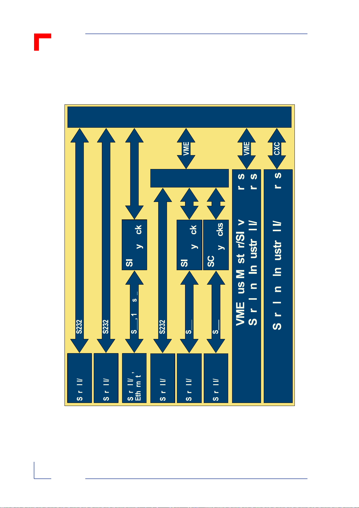
Figure 1-1: VSBC-32(E) System-Level Functional Block Diagram
VSBC-32 Mainboard (Master)
CXM-SIO3
*
Legend:
RS__[I]: RS232 non-optoisolated or RS485 optoisolated
10Base_: 10Base2 or 10Ba se5 or 10Base T Ethernet
* Serial I/O or Ethernet
Ethernet with VSBC-32E onl
ID 21168, Rev. 04Page 1 - 8 © PEP Modular Computers GmbH
Page 25
VSBC-32 Introduction
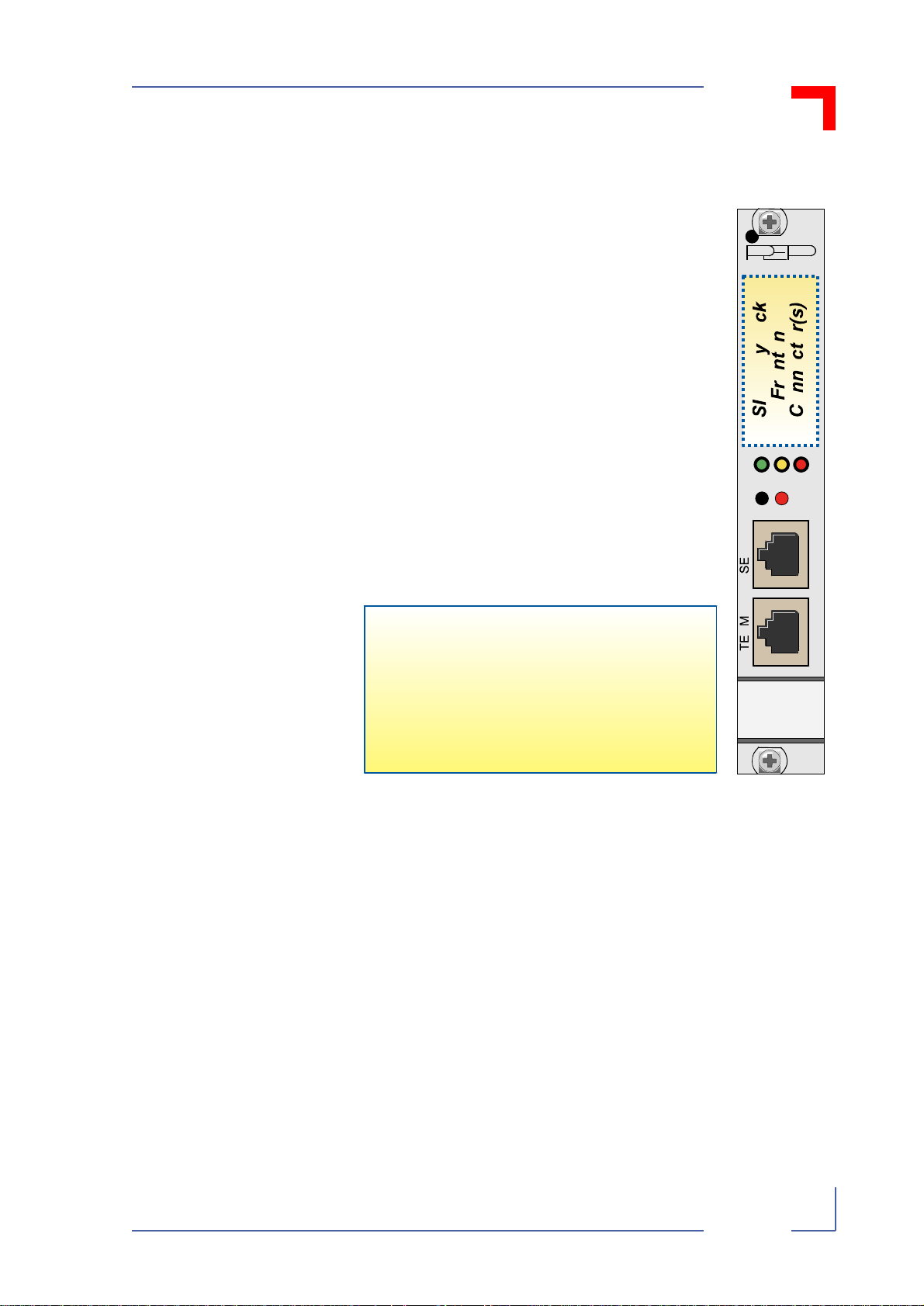
1.3.2 Frontpanels
Figure 1-2: VSBC-32 (E)
Frontpanel
LED’s:
• Green (“U”): General purpose
• Yellow (“W”): Watchdog
• Red (“H”): Halt
UWH
Pushbuttons:
• RST (left): Re set
• AB (right): Abort
RST AB
SI Piggyback Frontend Connector(s):
The additional frontend connector(s)
depend(s) on the type of serial interface
piggyback insta lled in combination with
the VSBC-32(E) mainboard. For any
details, please refer to the “Serial Interface Piggybacks” appendix in this manual.
VSBC-32
ID 21168, Rev. 04 Page 1 - 9© PEP Modular Computers GmbH
Page 26
VSBC-32 Introduction
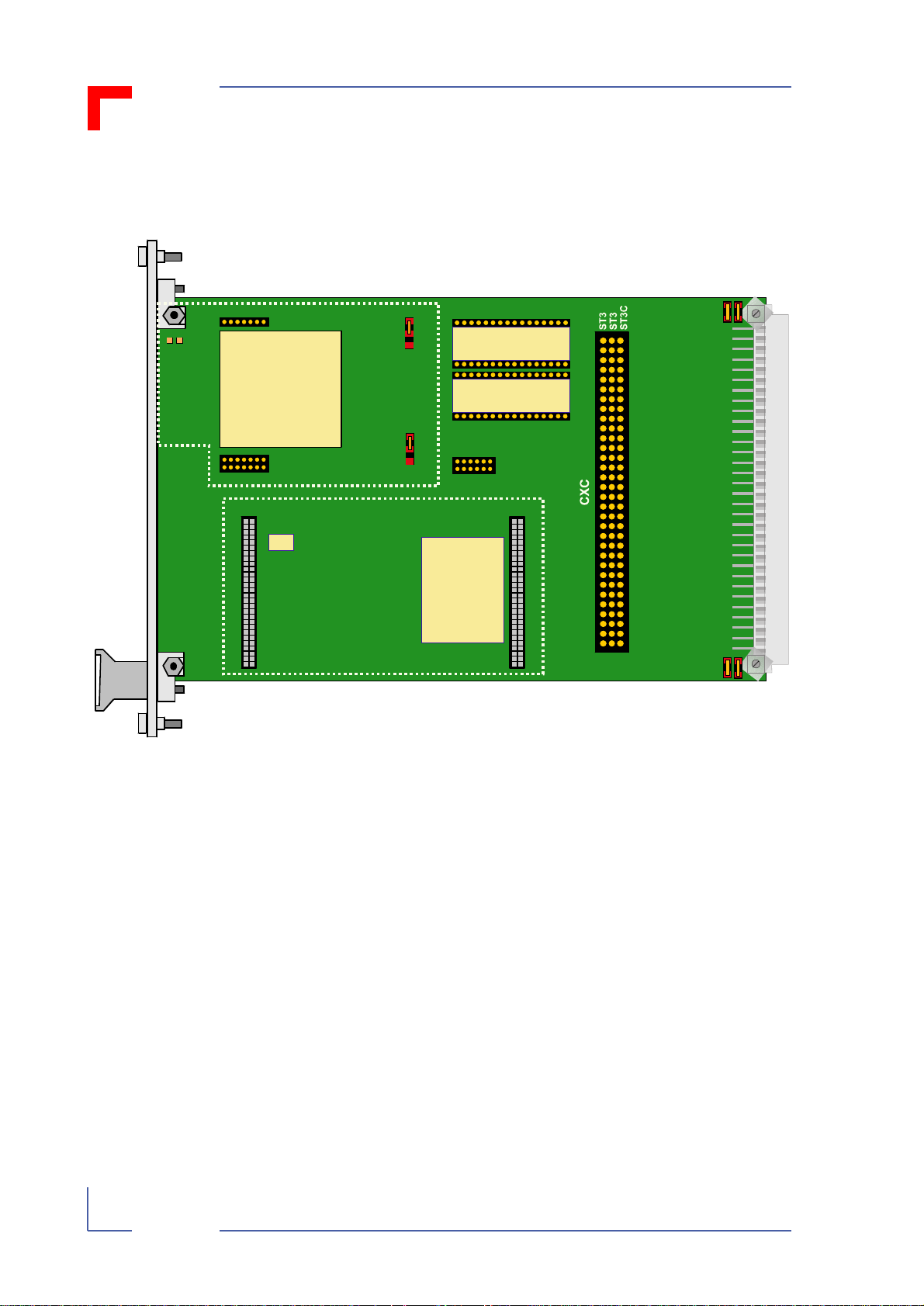
1.3.3 Board Layouts
Figure 1-3: VSBC-32(E) Board Diagram (front)]
J11J12
J6
17
ST2A
CPU / Serial
Communications
Controller
ST2B
ST2C
17
SI Piggyback
17 32
3
1
J14
2
FLASH/EPROM
(Upper Data)
116
17 32
FLASH/EPROM
(Lower Data)
116
3
1
J13
2
BDM
712
16
BU3
1492
EEPROM
SRAM
50
FLASH/EPROM:
Upper Data: D8-D15, even Byte addresses
Lower Data: D0-D7, odd Byte addre sses
BDM: Background Debug Mode.
Memory Piggyback
BU4
1492
50
J9J10
ID 21168, Rev. 04Page 1 - 10 © PEP Modular Computers GmbH
Page 27
VSBC-32 Introduction
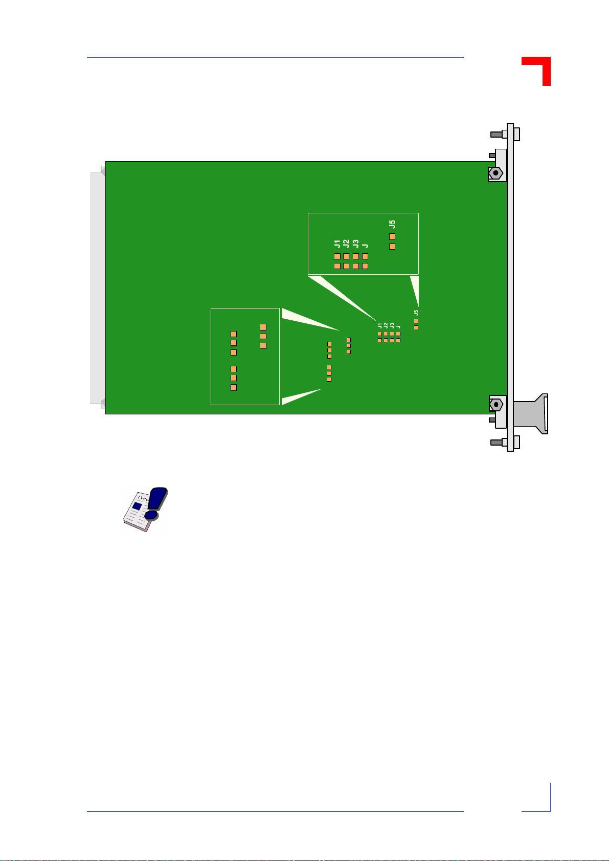
Figure 1-4: VSBC-32(E) Board Diagram (reverse)]
J11
J7
3
3
1
1
2
2
3
1
2
J8
J11
J7
3
3
1
1
2
2
3
1
2
J8
JUMPERS MAGNIFIED
Warn in g!
Solder jumpers are factory-set. To avoid possible damage to your
equiment, please do not alter them.
ID 21168, Rev. 04 Page 1 - 11© PEP Modular Computers GmbH
Page 28
VSBC-32 Introduction
1.4 Technical Specifications
Table 1-2: VSBC-32(E) Technical Specification (Sheet 1 of 3)
VSBC-32(E) Specifica tion
Board Variants
Combined CPU/Serial
Communica tio ns Co ntro lle r
On-Board Memory
Memory on Piggybacks
VMEbus Master/Slave
Functionality
Interrupt Control
• VSBC-32 : MC68360 processor,
• VSBC-32E: MC68EN360 processor
• MC68360: 25 MHz, no Ethernet capability
• MC68EN360: 25MHz or 33 MHz, Ethernet capability
CPU performance: Equivalent to Motorola CPU32
Serial I/O perfo rm.: RISC, 14 de dicate d D MA ch anne ls
• S RAM 256kB or 1MB (dual-p orte d,
backed-up by mean s of Gold -Cap s)
Note:
1MB with VSBC-32E only.
• EEPROM 2 kbit (serial); 1 kbit available
for applications
• Flash/EPROM 256kB or 1MB DIP EPROM/flash,
16-bit access
Minimum access ti me - 120n s
• DRAM 1, 4, 16 or 32 MB, 32-bit access
• F lash 0, 0.5, 1, 2 or 4 MB, 3 2-bit acc ess
• Mas ter A 24:D16 /D8, arbit ration , AM codes
• Slave A24:D16, dual-port RAM, mailbox IRQ
7-level CXC/VME IRQ handler, maskable via CXC/VME interrupt mask register; system vectors:
• ACFAIL* (via VME)Level 7 autovectored
• A bort Level 7 au tovect ored
• Tick Level 6 autovect ored
• M ailbox IR Q Level 5 autovect ored, mas kable
• SYSFAIL* Level 3 autovectored
16 on-board inte rrupt ers; level s/v ectors pro gramm able
Programmable Timers
Special Fun ction s
• Tick: Periodic-interrupt timer
• Watchdog: 512ms time-out for reset
• On-board bus error:8µs
• Ge neral-purp ose: 4*16 bit or 2*32 bit
Real-time cloc k (back ed-up):
• Date (year, month, week, day)
• Time (hour, minute, second)
2kbit serial EEPRO M:
• 1kbit for board specific data (serial number, IP address etc.)
• 1k bit for ap plicati on purpos es
DMA: 2 additional independent channels
(transfers between DRAM, FLASH, VME and CXC)
ID 21168, Rev. 04Page 1 - 12 © PEP Modular Computers GmbH
Page 29

VSBC-32 Introduction
Table 1-2: VSBC-32(E) Technical Specification (Sheet 2 of 3)
VSBC-32(E) Specification
Communication Standards
Mainboard Connectivity
Interface Ex pandib ility
• S erial I/ O (RS232, RS4 22, RS48 5)
• Ether net (VSBC-32E only)
• N on-op tois ola ted RS 232 se ria l int erfac e
(two RJ12 connectors, on frontpanel)
• One set of piggyback interface connectors for serial interface (SI) pig gyba cks (t wo 13-pi n ro w fe /male conn ect ors)
• One set of memory piggyback interface connectors
(two 50-pin row fe /m ale co nnec tors )
• B ackgroun d debug mode (BDM) interfa ce
(one 12-pin r ow m ale conn ector)
• VMEbus backplane interface
(one 96-pin D IN 41612, sty le C mal e co nnec tor)
• Enhanced CXC mezzanine interface
(one 96-pin D IN 41612, sty le C mal e co nnec tor)
Serial interface pi ggybac ks:
• SI-PB232: non-optoisolated RS232 serial interface
(two RJ45 connectors)
• SI-PB485-ISO: optoisolated RS485 serial interface
(two RJ45 connectors)
• S I-10B2: 10Base2 Ethernet int erface
(one RG58 coaxial connector)
• S I-10B5: 10Base5 Ethernet int erface
(one 15-pin DSUB female connector)
• S I-10BT: 10B aseT Et herne t in terfac e
(one RJ45 connector)
Note:
SI-10B_ with VSBC-32E only.
Front-End Functions
Data Retention
Power Supply
External serial interface modules:
• C XM-SIO3 Up to one modu le.
Pushbuttons:
• R eset but ton
• A bort button
LED’s:
• R ed: Halt
• Yellow Watchdog
• Gr een Gene ral purpo se
Short-term backu p (RTC and SRAM):
Via on-board gold-cap. Typ. 2µA/3V -> 150 hours
Long-term backup:
Via VME 5V stand-by line; automatic switching between 5V
stand-by and intern al gold -cap. Typ. 30µA/3V
Typically: 5V
With SI-PB5B: 12V
ID 21168, Rev. 04 Page 1 - 13© PEP Modular Computers GmbH
Page 30
VSBC-32 Introduction
Table 1-2: VSBC-32(E) Technical Specification (Sheet 3 of 3)
VSBC-32(E) Specifica tion
Power Consumption
Temperature Ranges
Humidity
Dimensions
Weight
• VSBC-32 : typ. 3.0W
• VSBC-32E: typ. 3.5W
Operation:
0° C to 70 °C (standard)
-40°C to +85°C (extended)
Storage:
-55°C to +125°C
0..95%, non-condensing
4HP/3U Eurocard (100mm x 160mm)
Mainboard: 130g
Serial inte rfac e pigg ybac k: 20..30g
Memory piggyb ack: 30g
1.5 Applied Standards
1.5.1 CE Com pliance
The
PEP Modular Computers’
ments of the following CE-relevant standards:
VMEbus and (e)CXC systems comply with the require-
• Emission EN50081-1
• Immission EN50082-2
• Electrical Safety EN60950
1.5.2 Mechanical Compliance
• Mechanical Dimensions IEEE 1101.10
1.5.3 Environmental Tests
• Vibration IEC68-2-6
• Permanent Shock IEC68-2-29
• Single Shock IEC68-2-27
ID 21168, Rev. 04Page 1 - 14 © PEP Modular Computers GmbH
Page 31

VSBC-32 Introduction
1.6 Related Publications
1.6.1 VMEbus/CXC Systems/Boards
• ANSI/VITA: VME64 Draft Specification 1-1994, Rev. 1.9
• VITA: CXC Specification, Rev. 2.0
•
PEP Modular Computers
•
PEP Modular Computers
•
PEP Modular Computers
•
PEP Modular Computers
1.6.2 Manufacturers’ Component Documentation
• Motorola: MC68EN360 Quad Integrated Communications Controller User’s Manual
• EM Microelectronic:V 3021 1-Bit Real- Time Clock Datasheet
• XICOR:X25C02 SPI Serial EEPROM Datasheet
CXC MPI Draft Specification, Rev. 3.1 (ID 12190)
CXC Reference Manual, ID 05263
CXM-SIO3 Manual (ID 14411)
CXM-SCCI Manual (ID 03545)
ID 21168, Rev. 04 Page 1 - 15© PEP Modular Computers GmbH
Page 32

This page was intentionally left blank.
ID 21168, Rev. 04Page 1 - 16 © PEP Modular Computers GmbH
Page 33

VSBC-32 Functional Description
Functional Description
Chapter
2
ID 21168, Rev. 04 Page 2 - 1© PEP Modular Computers GmbH
Page 34

This page was intentionally left blank.
ID 21168, Rev. 04Page 2 - 2 © PEP Modular Computers GmbH
Page 35

VSBC-32 Functional Description
2. Functional Description
2.1 General Information
The VSBC-32(E) is a 3U VMEbus combined system and communications controller
board based on the Motorola Quad Integrated Communications Controller “QUICC”
MC68(EN)360. Depending on the controller chip used and the SRAM size, there are
four board variants with different characteristics. The following table provides an overview of the various VSBC-32(E) board variants.
Table 1-1: VSBC-32(E) Board Variants
Board Name Proc esso r
VSBC-32
MC68360 — 25MHz 256kB
Ethernet
Capabilit y
+
VSBC-32E
MC68EN360
+
+
Being the MC68(EN)360 a CPU and serial communications contr oller, it is particularly
suitable for system control functions within applications with communications requirements such as LAN, WAN or fieldbusses (CAN, LON, PROFIBUS).
In fact, both the VSBC-32 and the VSBC-32E allow for a wide range of serial interfaces
based on the MC68(EN)360 controller which is able to handle up to six seri al communications channels. The channels can be configured in the following way:
• Two service / debug interface connectors (SMC interface, RxD/ TxD, RS232 only)
• Four full modem interface connectors / multiprotocol channels (SCC interfaces).
Thus, the VSBC-32(E) mainboard comes complete with two non-optoisolated RS232
external interfaces which are located on the lower half of the front panel. However, the
external serial interfacing can be extended by means of a variety of serial interface (SI)
piggybacks and/or a CXM-SIO3 type external serial interface module. This external module can be either “sandwiched” with the controller or placed to the right of the VSBC-32(E).
In the first case, communication between the controller and the I/O module is acchieved
via the VSBC-32(E)’s on-board CXC connector, in the second case via the VMEbus.
Processor
Frequency
25MHz 256k B
33MHz 256k B
33MHz 1MB
SRAM Size
As the CXM-SIO3 can be used again as a carrier for various serial interface (SI) and
serial communications (SC) piggy backs, the VSBC- 32/CXM-SIO3 tandem r epresents a
really powerful and versatile sytem control and serial communications control set.
Together with the two service/debug interfaces, a maximum of three (four with the serial
interface piggyback fitted) completely configured serial interfaces are available for the
base board. Three (two with serial interface piggy back fitted) serial interfaces may be
configured via the VMEbus where three of the four full modem Interfaces are routed.
The VSBC-32(E) allows also a significant variety of memory configurations, mainly
DRAM and flash memory located on special memory piggybacks, add-on flash/EPROM
on DIP s ockets, battery backed-up SRAM and EEPROM.
ID 21168, Rev. 04 Page 2 - 3© PEP Modular Computers GmbH
Page 36

VSBC-32 Functional Description
2.2 Specifics
2.2.1 System Control Functionality
Under the aspect of system control the on-chip 32-bit CPU core of the Motorola
MC68(EN)360 provides system integration at different processor frequencies. The processor core acts essentially as a Motorola CPU32 microprocessor operating at 25MHz or
33MHz without cache memory. In addition, the MC68(EN)360 offers background debugging via the on-chip “Background Debug Mode” which allows direct communication with
the CPU.
To act as a system controller, the VSBC-32(E) is provided with arbiter, system clock
driver, power monitor with system reset driver, IACK daisy chain driver and 7-level
VMEbus interrupt controller.
Arbitration is single-level FAIR (compare VME64 Specification Rule 3.14/Observation
3.17). If the VSBC-32(E) is used as a system controller and consequently placed in the
VMEbus backplane’s system slot, a special detection function provided by the board
makes any “slot 1” jumper setting superfluous. The VSBC-32(E) also provides a bus
monitor for the VMEbus.
Interrupt Control
The interrupt control logic of the MC68(EN)360 processes internal interrupt requests
alongside with external autovectored interrupt requests and a “mailbox” interrupt request
from the VMEbus control/status register. The interrupt control logic is built up using the
processor’s internal interrupt control and an external IRQ7 interrupt handler.
Internal requests are related to all interrupt requests caused by the controller sources,
including the processor’s system integration functions (watchdog timer, periodic interrupt timer) and the communications processor module (RISC controller, timers, DMA’s,
SCC’s etc.).
In order to avoid conflicts regarding the different interrupt levels, it is recommended to
use IRQ level 4 for the MC68(EN)360 CPU internal requests and IRQ level 6 for the
MC68(EN)360 serial controller internal requests.
In addition, external interrupt sources can generate autovectored interrupts and an
external VMEbus master may require an interrupt by setting a “mailbox” IRQ in the
VMEbus control/status register.
For any detailled information as well as a complete list of the Motorola
controller signals please refer to the relating Data Sheet.
®
MC68(EN)360
ID 21168, Rev. 04Page 2 - 4 © PEP Modular Computers GmbH
Page 37

VSBC-32 Functional Description
Table 2-2: External Autovector and Mailbox Interrupts
Source Interrupt Source Interrupt Type
ABORT / ACFAIL MC68(EN)360, pin IRQ7 Aut ovecto r 7
Reserved MC68 (EN)36 0, p in IRQ6 Aut ovec tor 6
Mailbox IRQ MC68(EN)360, pin IRQ5 Autovector 5
Reserved MC68 (EN)36 0, p in IRQ4 Aut ovec tor 4
SYSFAIL MC68(EN)360, pi n IRQ3 Autov ector 3
Reserved MC68 (EN)36 0, p in IRQ2 Aut ovec tor 2
Reserved MC68 (EN)36 0, p in IRQ1 Aut ovec tor 1
Mailbox Pendi ng Bit P_IR Q5 Control/stat us r egiste r
2.2.2 Memory Configurations
The VSBC-32(E) allows a significant variety of memory configurations. The special
DRAM/flash piggybacks (DM60x), for instance, allows the user to take advantage of the
on-board programming facility to produce low cost upgrades by simply overwriting existing stored data. This memory can be configured with different memory options allowing
remarkable flexibility when customizing memory requirements for real-time applications.
The DM60x piggybacks provide between 1MB and 64MB o f DRAM with 32-bit access
and up to 4MB of +5V flash memory. In addition, a set of DIP sockets located on the
VSBC-32(E) mainboard allows the installation of an additional 1MB of flash/EPROM.
Both memory devices can be used for bootstrapping. The selection of the boot memory
is achieved by hardware jumpering.
Note...
Physically the DM60x piggybacks provide up to 64MB of DRAM.
However, the IUC-32(E) mainboard envisages addre ssing for up to
two memory banks of 6 4MB each.
Exchange and retention of system relevant data from the VMEbus to the CPU/DMA and
viceversa is provided by means of 256kB or 1MB of a 16-bit wide dual-ported SRAM
which is backed-up using Gold Caps. Both the VMEbus users and the on-board CPU
have access to the SRAM memory.
Note...
The upper 8kB of dual-ported SRAM are accessed by the
VMEbus, the lower 8kB a re reserved for mailbox interru pts.
Configuration data are stored in a 2kbit EEPROM. 1kbit is used for factory-specific configuration purposes, and 1kbit is available for application-specific configuration data.
ID 21168, Rev. 04 Page 2 - 5© PEP Modular Computers GmbH
Page 38

VSBC-32 Functional Description
ggy
A schematic overview of all possible memory c onfigurations is given in the fi gure on the
next page.
Figure 2-1: VSBC-32 Memory Configuration Variants
VSBC-32
MC68360
25MHz
VSBC-32E
MC68EN360
25MHz
33MHz
CPU Options
SRAM
256kB
SRAM
256kB
or
SRAM
1MB
2kbit EEPROMRTC
CPU/Serial
Comm.
Controller
Flash
or
EPROM
(256kB or
1 MB)
Memory Pi
- 1MB DRAM + 0 or 1 MB Flash EPROM
- 4MB DRAM + 1,2 or 4 MB Flash EPROM
- 8MB DRAM + 1,2 or 4 MB Flash EPROM
- 16MB DRAM + 1,2 or 4 MB Flash EPROM
- 32MB DRAM + 0.5,1 or 2 MB Flash EPROM
- 64MB DRAM + 1,2 or 4 MB Flash EPROM
backs
SRAM
DRAM
+
Flash
Mainboard
2.2.3 DMA Channels
Two independent channels are provided by the MC68(EN)360 controller chip and can
be used by applications requiring data transfer between VMEbus modules (as well as
CXC modules, if present), DRAM, flash memory and dual-ported SRAM.
Memory-to-memory transfers with the DMA’ s of the MC68(EN)360 are possible with any
combination of on-board and VMEbus addresses.
ID 21168, Rev. 04Page 2 - 6 © PEP Modular Computers GmbH
Page 39

VSBC-32 Functional Description
2.2.4 Serial Communications Control
Under the aspect of serial communications control, a major advantage of the
MC68(EN)360 serial communications controller cor e SIM60 is its compatibility with all
important communication standards. A detailled description of all control functions is
provided on the following pages alongside with a comprehensive list of the possible
serial interface piggybacks and their connectors.
For the mainboard interface connector pinouts refer also to the “Board Interfaces” section of this chapter. For a description and pinouts of the connectors of the serial interface/communication piggybacks as well as of the CXM-SIO3 frontpanel interface
connectors please refer instead to the “SI Piggy backs” appendix of this manual as well
as to the CXM-SIO3 user’s manual and its “Serial Communications Piggybacks” appendix respectively.
Communication Standards and Protocols
Six communication standards are available on the VSBC-32(E):
• Serial I/O (RS232, RS485; RS422)
• Ethernet (10Base2, 10Base5, 10BaseT)
Serial communications using the RS232 standard are available on the VSBC-32(E)
mainboard frontpanel as well as on a dedicated piggy back to be connected to its SI
Interface. In addition, RS232 communication is possible via a CXM-SIO3 external serial
interface module. Communications using the PROFIBUS protocol are supported by an
optoisolated, half-duplex RS485 serial I/O interface implemented on a dedicated piggy back to be connected to the SI Interface of either the VSBC-32(E) or the external serial
interface module. RS422 is not commonly available on the VSBC-32(E) but can be supplied by
The MC68(EN)360 processor is specified to support also a full set of IEEE 802.3/Ethernet CSMA/CD media access control and channel interface functions. Since the controller requires an external interface adapter and transceiver function, the Ethernet
interface can be adapted to all standard Ethernet functions, such as 1 0Base T, 10Base5
and 10Base2 via a piggyback connected to the SI Interface on the VSBC-32(E).
PEP Modular Computers
on special request.
Note...
The CXC bus does not support a 12V power supply. Therefore,
the 10Base5 Et hernet piggyback SI-10B5 ca nnot be used on the
IUC-32(E) controller bo ard.
Serial I/O Channelling
The VSBC-32(E) mainboard is provided with TxD and RxD signals by the controller’s
SMC1 and SMC2 channels and supply RS232 interface software handshake (XON/
XOFF) capability. They are configured as service/debug connectors by default.
All full modem interfaces located on the piggybacks and/or CXM-SIO3 external serial
interface module supply RxD, TxD, RTS, CTS, CD, DTR and RCLK/TCLK. Two of the
full modem interfaces can be configured on the piggyback interface with a variety of
ID 21168, Rev. 04 Page 2 - 7© PEP Modular Computers GmbH
Page 40

VSBC-32 Functional Description
ggy
y
serial interface (SI) piggybacks (RS232, RS485, Ethernet). The SCC1 channel of the
MC68(EN)360 provides the interface to the ser ial interface (SI) piggyback installed on
the VSBC-32(E). All other channels of the controller (SCC2, SCC3 and SCC4) are
ported to the CXC interface except for the SI-PB232 piggyback which has on-board
additional control provided by the SCC4 channel through the piggyback interface for
serial interface piggybacks.
Thanks to the fact that three out of four SCC channels ar e routed to the CXC interface
connector, also an CXM-SIO3 external serial i nterface module can be installed in the
system, which therefore becomes a sort of “privileged” serial I/O extension of the VSBC32(E) board itself. In addition to two non-optoisolated RS232 serial interface connectors
the external serial interface module supports again a serial interface piggyback and up
to three serial communications piggy backs with the relating interfacing options. Maximum one CXM-SIO3 module can be cont rolled by an VSBC-32(E) board.
Figure 2-2: MC68(EN)360 Serial Communication Channeling
MC68(EN)360
Rx and Tx onl
SCC2
SCC3
SCC4
SCC1
SMC2SMC1
}
}
RS232
RS232
CXC Interface:
RS232, RS432, RS485
Ethernet (10Base2,
10Base5, 10BaseT)
SI Pi
Interface:
RS232, RS432, RS485
Ethernet (10Base2,
10Base5, 10BaseT)
back
Note...
The serial channel SCC4 is routed to both the piggyback interface for serial interface p iggyb acks a nd th e CXC and c an be used
by either one or the other, not both at the same time.
ID 21168, Rev. 04Page 2 - 8 © PEP Modular Computers GmbH
Page 41

VSBC-32 Functional Description
Depending on whether the piggyback interface for serial interface (SI) piggybacks is
configured as an Ethernet port (board versions with Ethernet piggyback) or not, the
serial interfaces channels of the VSBC-32(E) can assume the functions described in the
following figure.
Figure 2-3: VSBC-32(E) Serial Interface Channel Configurations
Port
Service/Debug 1 SMC1 Main board, upper RJ12
Service/Debug 2 SMC2 Main board, lowe r RJ12
Ethernet
Full MODEM 1
Full MODEM 2 SCC2 External serial inte rface module
Full MODEM 3 SCC3 External serial inte rface module
Full MODEM 4 SCC4
Legend:
Board versions with Ethernet port
Board versions without Ethernet port
Independent of Ethernet configuration
1
SCC4 is not used by any of the Ethernet piggybacks. With these piggybacks, SCC4 can be used on the C XC bus.
Serial Communicati on
Channel
SCC1 Mainboard, serial in terface pig gyback
Interface Location
External serial i nterface module
Mainboard or
Serial interface piggyback or
External serial i nterface module
1
ID 21168, Rev. 04 Page 2 - 9© PEP Modular Computers GmbH
Page 42

VSBC-32 Functional Description
* S i l I/O PROFIBUS ( Eth t)
2.3 Functional Block Diagram
Figure 2-4: VSBC-32 Board-Level Functional Block Diagram
System Controller
Subordinbate CPU Control Functions
System
Controller Core
Subordinbate CPU Memory Functio ns
Memory
Piggyback
Serial Communications Controller
SMC1 SMC2 SCC1 SCC4 SCC3 SCC2
CXC B u s
CXM-SIO3
CXC
Controller Logic
VMEbus
VMEbus
*
Legend:
RS___: RS232 non-optoisolated or RS485 optoisolated
10Base_:10Base2 or 10Base5 or 10BaseT Ethernet
ID 21168, Rev. 04Page 2 - 10 © PEP Modular Computers GmbH
Page 43

VSBC-32 Functional Description
Fi
f
2.4 Board Interfaces
The following section provides a description of the mainboard interface connector
pinouts. For a detailled list and description of the connectors of the serial interface/communication piggybacks and of the frontpanel interface connectors please refer to the “SI
Piggybacks” appendix of this manual a s well as to the CXM-SIO3 user’s manual and its
“Serial Communications Piggyba cks” appendix respectively.
2.4.1 Serial I/O Interfaces
The mainboard RJ12 RS232 frontpanel connectors BU7 and BU8 of the VSBC-32(E) are provided with TxD and RxD signals by the controller’s
SMC1 and SMC2 channe ls and supply RS232
interface software handshake (XO N/XOFF) capability. They are configured as service/debug connectors by default.
The pinouts of the RJ12 connectors are shown in
the following table.
Table 2-3: Pinouts of the Mainboard Serial Interface Connectors BU7/BU8
Pin Pinouts
1N/C
2GND
3TxD
4RxD
gure 2-5: Orientation o
the VSBC-32(E) Mainboard
Serial Interfaces
1
SMC1
6
1
SMC2
6
5N/C
6N/C
N/C = Not connected.
ID 21168, Rev. 04 Page 2 - 11© PEP Modular Computers GmbH
Page 44

VSBC-32 Functional Description
2.4.2 Piggy back Interface Connectors for Serial Interface Piggybacks
The VSBC-32(E) is equipped with a set of piggyback interface connectors for serial
interface (SI) piggybacks (three 7-pin row male connectors). The pinout of these piggyback interface connectors includes all signals for serial I/O (RS232), PROFIBUS
(RS485) and Ethernet (10BaseT, 10Base5, 10Base2) communication.
Note...
Although physically all piggybac ks fit on bott basic board variant s
(IUC-32 and IUC-32E), the MN68360 processor of the IUC-32
variant does not support Ethernet communication. Therefore,
Ethernet piggybacks should be used only on the IUC-32E board
variants.
For a detailled description of the pinouts of these piggyback interface connectors please
refer to the VITA/
PEP Modular Computers
CXC MPI Specification.
2.4.3 Memory Piggyback Interface Connectors
The VSBC-32(E) is equipped with a set of memory piggyback interface connectors (two
50-pin row female connectors). The pinout of these piggyback interface connectors
includes all signals for t he con nection of u p to 128M B of DR AM and up to 4 MB o f flash
EPROM.
For a detailled description of the pinouts of these piggyback interface connectors please
refer to the VITA/
PEP Modular Computers
CXC MPI Specification.
2.4.4 EPROM DIP Sockets
The VSBC-32(E) is equipped with two sets of (flash) EPROM DIP sockets (two 32-pin
row female sockets). The pinout of th es e DIP s oc kets includes all signals for the connection of up to 1MB of SRAM.
ID 21168, Rev. 04Page 2 - 12 © PEP Modular Computers GmbH
Page 45

VSBC-32 Functional Description
2.4.5 Background Debug Mode Interface Connector
The VSBC-3 2(E ) is equipped wi t h a b ackground debu g mode (BDM) in terface connector
(one 12-pin row male connector). This connector allows an external debugger to be
interfaced to the MC68(EN)360 for controlling purposes. The interface connector is
specified by Motorola.
The pinouts of the BDM interface connector are shown in the following table. For any
further details, please refer to the Motorola MC68(EN)360 User ’s Manual.
Table 2-4: BDM Interface Connector Pinouts
Pin Signal Pin Signal
1GND 2CLKO1
3 DS* 4 BERR*
5 GND 6 BKPT * / DSCL K
7GND 8FREEZE
9 RESETH* 10 IFETCH / DSI
11 VCC 12 IPIPE0 / DSO
2.4.6 VMEbus Backplane Interface
The VSBC-32(E) is equipped with a VMEbus backplane interface connector.
The board is provided with a complete ma ster inter face f or the VMEbus backplane con-
nector. The VMEbus master interface consists of a VMEbus arbiter, requester, system
controller and buffers for data/address/control signals. Simultaneously, the VSBC-32(E)
can act as a VMEbus slave, as it is provided with a slave interface which consists of a
programmable board address decoder, a dual-ported SRAM access and a mailbox
interrupt controller.
To act as a system controller, the VSBC-32(E) is provided with arbiter, system clock
driver, power monitor with system reset driver, IACK daisy chain driver and 7-level
VMEbus interrupt controller.
Arbitration is single-level FAIR (compare VME64 Specification Rule 3.14/Observation
3.17) on BR3*. If the VSBC-32(E) is used as a system controller, a special detection
function provided by the board, which is also readable within the VMEbus control/status
register, makes any “slot 1” jum per setting superfluous. The VMEbus int erru pt acknowledgement is controlled via a daisy chain driver that is supplied with the board. IACK* is
connected via the VMEbus backplane for IACKIN* of the system slot.
The signals SYSCLK* and SYSRES* can be routed from on-board to the VMEbus
through the use of jumpers, leaving to the VMEbus user instead of the system controller
the initiative of generating these signals. SYSFAIL* generates a maskable on-board
autovectored level-3 interrupt (please refer also to the section System Control Functionality (Interrupt Control) of this chapter), whereas ACFAIL* generates a non-maskable
on-board level-7 interrupt.
ID 21168, Rev. 04 Page 2 - 13© PEP Modular Computers GmbH
Page 46

VSBC-32 Functional Description
The VSBC-32(E) also provides a bus monitor for the VMEbus. A 128µs bus error timer
monitors the cycle le ngths of the VMEb us data tra ns fer and generate s a V MEbus BERR*
signal on timeout. This timer is enabled and disabled via the VMEbus control/status register which conta ins a lsao a timeout statu s bit in order to ide ntify th e bus e rrors g enerate d
by the bus monitor.
Exchange and retention of system relevant data from the VMEbus to the CPU/DMA and
viceversa is provided by means of 256kB or 1MB of a 16-bit wide dual-ported SRAM
which is backed-up using Gold Caps. Both the VMEbus users and the on-board CPU
have access to the SRAM memory (upper 8kB, i.e. even Byte addresses).
Note...
The dual-ported SRAM cannot be accessed through its own
VMEbus interface. A bus monitor timeout would result due to the
fact that any access by the VMEbus to the DPRAM would be
blocked as long as the VSBC-32(E) is bu s master.
An external VMEbus master may interrupt the VSBC-32(E) by setting P_IRQ5 (“mailbox
interrupt pending”) in the VMEbus control/status register. Seen from the VMEbus, the
address of this dual-ported register is identical to the base address of the dual-ported
SRAM (lower 8kB, i.e. odd Byte addresses).
Note...
All bits of the VMEbus control/status register can be read from
the VMEbus, but only th e bit P_IRQ5 is read /write.
For a complete map of the VMEbus control/status register please refer to the relating
section in the Configuration chapter of this manual.
For any general VMEbus information including generic pinouts please refer to Appendix
B of the ANSI/VITA VME64 Specification.
2.4.7 CXC Mezzanine Interface
The VSBC-32(E) is equipped with a CXC mezzanine interface connector.
CXC and eCXC both contain a 16-bit data bus, seven address lines and eight decoded
chip select lines. In total, there are eight control signals (CXC_CS0...CXC_CS7). The
base address of the CXC can be programmed via the CS5 line of the MC68(EN)360.
The main difference between the two VITA standards is the amount of address space
available for peripheral devices:
• CXC: 8*256Bytes (overall length: 0x400H, 1024Bytes actually av ailable)
• eCXC: 8*16MB (overall length: 0x1000 000, 16MB actually available)
Furthermore, the (e)CXC contains a 4-IRQ capability (4 edge-sensitive interrupt
requests), DMA capability (1 channel, DREQ + DACK), serial ports (3 channels, Full
MODEM) and a set of parallel port signals. These special CXC functions are based on
the MC68(EN)360 controlle r reso urc es.
ID 21168, Rev. 04Page 2 - 14 © PEP Modular Computers GmbH
Page 47

VSBC-32 Functional Description
For general CXC information, including generic pinouts and a comparison of the
MC68(EN)360 and the MC68302 CPU pinouts on the CXC, please refer to the “CXC”
appendix attached to this manual, the
or to the CXC Specification.
2.5 VSBC-to-VSBC-32 System Upgrading
In the following the porting information required by customers w anting to upgrade their
VSBC-based systems to an VSBC-32 based one is supplied.
The VMEbus/CXC ports SER1, SER2 and SER3 of the MC68302 are equivalent to
ports SCC2, SCC3 and SCC4 respectively on the MC68(EN)360 controller chip.
With regard to special VMEbus/CXC capabilities, the VMEbus/CXC pinout on the
VSBC-32(E) has been developed to provide maximum compatibi lity between the standard VMEbus/CXC functions. In addition, all signals are available in order to configure
two time division multiple xed channels via the VMEb us/CXC (ISDN, PCM, GCI and so on).
PEP Modular Computers
CXC Reference Manual
Multifunction pins with incompatible functions with regard to the MC68302 and
MC68(EN)360, which are called “user-defined” in the generic CXC Specification, are not
part of the VSBC-32(E) VMEbus or CXC specification.
Although the SMCs are configured on the mainboard, these ports are also integrated on
the VMEbus/CXC because of possible ISDN applications where SMCs can be integrated and other protocols supported by the M C 68(EN) 3 60.
Note...
If the RCLK2 signal (VMEbus/CXM pin C16) is required, jumper
J4 (24MHz clock) must be opened and the serial drivers delivered by
PEP Modular Computers
must be modified.
ID 21168, Rev. 04 Page 2 - 15© PEP Modular Computers GmbH
Page 48

VSBC-32 Functional Description
Table 2-5: IUC/IUC- 32 Por tin g Information (Sheet 1 of 2)
CXC
Function
IRQ_1 A1 Yes PC0 —
IRQ_2 A2 Yes PC1 —
IRQ_3 A3 Yes PC2 —
IRQ_4 A4 Yes PC3 —
DMA_ACK C2 Yes PB5 —
DMA_REQ C3 Yes PB4 —
SER1_RCLK B1 Yes PA8 —
SER1_TCLK B2 Yes PA10 —
SER1_TXD B4 Yes PA3 —
SER1_RXD B10 Yes PA2 —
SER1_RTS B5 Yes PB13 —
SER1_DTR A13 Yes PB17 —
SER1_CTS B13 Yes PC6 —
SER1_CD B14 Yes PC7 —
SER2_RCLK C16 Yes PA13 Cannot be used if J4 is set 3
Pin
MC68302
HW
Comp.
MC68(EN)
360
Port
Comment
See
Note
SER2_TCLK C15 Yes PA12 —
SER2_TXD C17 Yes PA5 —
SER2_RXD C18 Yes PA4 —
SER2_RTS C12 Yes PB14 —
SER2_DTR A11 Yes PB16 —
SER2_CTS C13 Yes PC8 —
SER2_CD C11 Yes PC9 —
SER3_RCLK C6 Yes PA15 Not usable if SI piggyback uses SCC4 4
SER3_TCLK C5 Yes PA14 —
SER3_TXD C8 Yes PA7 Not usable if SI piggyback uses SCC4 4
Legend:
1 Reserved Pin: On a standard VSBC-32 board, this signals is used for UART ports at BU7 and BU8.
2 Reserved Pin: On a standard VSBC-32 board, this signal is used for SPI to which the EEPROM is already con-
nected. PB0 is chip select of the EEPROM.
3 Reserved Pin: On PA13, a 24 MHz clock signal is routed via jumper J4. This signal is alw ays needed for PEP
standard software (serial drivers).
4 Dual Functioning Pin: This signal is routed both to the mainboard’s interface for serial interface piggybacks
(ST5C) and the CXC backplane connector and can be used by either one or the other, but not both at the same
time. Due to this, a conflict exists if the SCC4 port is to be used with the SI232 piggyback and CX C boards
(such as CXM-SIO3), as both boards access this port. The SCC4 port can, therefore, not be used at the same
time by serial interface piggybacks and CXC boards.
ID 21168, Rev. 04Page 2 - 16 © PEP Modular Computers GmbH
Page 49

VSBC-32 Functional Description
Table 2-5: IUC/IUC-32 Porting Information (Sheet 2 of 2)
CXC
Function
SER3_RXD C9 Yes PA6 Not usab le if SI pi ggyba ck use s SCC 4 4
SER3_RTS B7 Yes PB15 Not usable if SI pi ggyba ck u ses SC C4 4
SER3_DTR A12 Yes PB9 Not usable if SI piggyback uses SCC4 4
SER3_CTS B16 Yes PC10 Not u sab le if SI pi ggyba ck u ses SC C4 4
SER3_CD B8 Yes PC11 Not usable if SI piggyback uses SCC4 4
User-Defined
Pin
A5 No PB0
A6 No PB1
A8 No PB2
A9 No PB3
A10 No PB8 See MC68360 User Manual
B11 No PB10 Used on board SMC2 (Transmit) 1
C1 No PB6 Used on board SMC1 (Transmit) 1
MC68302
HW
Comp.
MC68(EN)
360
Port
Comment
Used on board SPI SEL for EEPROM.
Cannot be used on CXC
SPI Clk: can be used if an ‘SPI SEL’
other than PB0 is used.
SPI TxD: can be used if an ‘SPI SEL’
other than PB0 is used.
SPI RxD: can be used if an ‘SPI SEL’
other than PB0 is used.
See
Note
2
C4 No PB11 Used on board SMC2 (Receive) 1
C10 No PB7 Used on board SMC1 ( Recei ve) 1
Legend:
1 Reserved Pin: On a standard VSBC-32 board, this signals is used for UART ports at BU7 and BU8.
2 Reserved Pin: On a standard VSBC-32 board, this signal is used for SPI to which the EEPROM is already con-
nected. PB0 is chip select of the EEPROM.
3 Reserved Pin: On PA13, a 24 MHz clock s ignal is routed via jumper J 4. This signal is al ways needed for PEP
standard software (serial drivers).
4 Dual Functioning Pin: This signal is routed both to the mainboard’s interface for serial interface piggybacks
(ST5C) and the CXC backplane connector and can be used by either one or the other, but not both at the same
time. Due to this, a conflict exists if the SCC4 port is to be used with the SI232 piggyback and CXC boards
(such as CXM-SIO3), as both boards access this port. The SCC4 port can, therefore, not be used at the same
time by serial interface piggybacks and CXC boards.
ID 21168, Rev. 04 Page 2 - 17© PEP Modular Computers GmbH
Page 50

VSBC-32 Functional Description
2.6 Special Board Functions
2.6.1 Rea l-Time Clock
The three-wire serial interface real-time clock V3021 is a 1-bit device which is accessible over the CS6 of the MC68(EN)360. Its time-keeping features include as follows:
seconds, minutes, hours, day of mon th, month , year, week day and week number in B CD
•
format;
• leap year and week number correction;
• stand-by supply smaller than 1µA.
For further information p
manual and the EM Microelectronic V3021 data sheet.
lease refer also to the “Software Configuration” chapter in this
2.6.2 EEPROM
The serial EEPROM is a 1-bit device which is accessible over the three- wire Interchip
SPI Interface of the MC68(EN)360. The first half of the EEPROM (1 kbit) is reserved for
factory data, including Board ID codes, Internet/Ethernet addresses, boot information
etc. The second half of the EEPROM is available for the user. See also the Software
Configuration chapter
For further information on the EEPROM, please refer also to the XICOR X25C02 data
sheet.
in this manual.
2.6.3 PLL Opera ti on Mode
The MC68(EN)360 inputs EXTAL and CPU clock use the same input frequency. The
XT AL input is left open. The clock mode is selected via the hard-wired inputs MODCLK0
and MODCLK1. With the default settings of MODCLK0 = 1 and MODCLK1 = 0, the following configuration is selected:
no prescaler;
•
• multiplication factor = 1;
• CLKIN to the prescaler = CPU clock;
• internal frequency (VCO/2) = CPU clock;
2.6.4 Tick Generator
The MC68(EN)360 internal Periodic Interrupt Timer is used b y the
ing system as Tick generator.
For further information please refer also to the Motorola MC68(EN)360 User ’s Manual.
PEP
real-time operat-
ID 21168, Rev. 04Page 2 - 18 © PEP Modular Computers GmbH
Page 51

VSBC-32 Functional Description
2.6.5 Bus Error Timers
The VSBC-32(E) provides an on-board bus error timer and a VMEbus error timer.
There are three cases of bus error
Table 2-6: Bus Error Types
Cause Timeout Enable / Disable
Reserved address BERR0 100ns Permanently enabled
:
On-board BERR1 8µs
VMEbus BERR2 128µs
Enable / disable possible,
set in board control registe r
Enable / disable possible,
set in VMEbus control register
On-Board Bus Error Timer
An 8µs timeout on-board timer monitors the cycle lengths of data transfers to and from
locations beyond the CPU data bus buffer, including on-board I/O, VMEbus, SRAM and
CXC. After a timeout occurs, it generates an on-board bus error signal for error termination. This timer is enabled/disabled via the board control/status register, which also supplies a timeout status bit in order to identify bus errors generated by the on-board bus
error timer.
During VMEbus cycles the on-board bus error timer is reset as soon as the VSBC-32(E)
gains VMEbus ownership, i.e. the time gap between a VMEbus request and the starting
of the VMEbus cycle is monitored by the on-board bus error timer. The VMEbus cycles
themselves are monitored by the separate VMEbus error timer.
Note...
The internal MC68(EN)360 bus error timer (hardware watchdog
timer) is not used on the VSBC-32(E). Therefore, it should
remain disabled (default setting).
VMEbus Error Timer
In addition to the on-board bus error timer, the VSBC-32(E) provides a bus monitor for
the VMEbus. A 128µs timer monitors VMEbus data transfer cycle lengths and generates
a VMEbus bus error signal BERR* for er ror termination. This error is enabled and disabled via the VMEbus control/status register which also supplies a timeout status bit in
order to identify bus errors genrated by the bus monitor.
For a complete map of the VMEbus control/status register please refer to the relating
section in the Configuration chapter of this manual.
ID 21168, Rev. 04 Page 2 - 19© PEP Modular Computers GmbH
Page 52

VSBC-32 Functional Description
2.6.6 Watchdog Timer
A 512ms watchdog timer triggers the on-board reset generator at timeout. Once
enabled via the board control/status register, the watchdog timer cannot be reset by
software. It must be re-triggered via the corresponding bit in the board control/status
register periodically within the timeout period. ‘Watchdog t imer running’ is a status that is
displayed by the yellow front panel LED.
For the location of the Watchdog LED please refer to the VSBC-32(E) Frontpanel figure
in the “Introduction” chapter of this manual.
2.6.7 Reset Sources
The VSBC-32(E) interacts with the following reset sources:
Table 2-7: VSBC-32(E) Reset Sources
Reset Source Identification
Push Button No
SYSRES* VME No
Watchdog WDG bit on-board (Board Control/Status Register)
Power Monitor ( 4.65V ) Inside the MC68(EN )360
2.6.8 “Slot 1” Detection
During power-up the VSBC-32(E) dete cts whether it is being used as a system controller (slot 1). This information can be read from the VMEbus control/status register and is
valid until the next power-down of the sy stem.
For a complete map of the VMEbus control/status register please refer to the relating
section in the Configuration chapter of this manual.
ID 21168, Rev. 04Page 2 - 20 © PEP Modular Computers GmbH
Page 53

VSBC-32 Functional Description
2.7 Frontpanel Functions
The frontpanel status indicators consist of three LED’s with the following functions:
• Yellow Watchdog LED
• Green General Purpose
• Red CPU Halt or Reset
The green LED is user-defined by the customer. It is set by the software during startup
when the MC68(EN)360 is initialized.
Figure 2-6: VSBC-32(E)
Frontpanel LED and
Button Locations
Legend:
Yellow Watchdog LED
Green General Purpose
Red CPU Halt or Reset
RST Reset Button
AB Abort Button
A Reset button is fitted to the front panel to avoid false operation. The Reset button triggers the on-board system reset generator. In addition, an Abort button is also fitted to
the front panel. The Abort button generates a non-maskable level- 7 interrupt which is
used for debugging purposes.
WUH
RST AB
2.8 RTC and SRAM Data Retention
Short-term data retention for RTC and SRAM is gained with two Gold Caps, each with a
value of 0.22 Farad. In contrast to Lithium cells, Gold Caps do not require servicing.
This short-term backup is intended for short power failures or for reconfiguring systems.
An empty Gold Cap needs approximately three hours to charge up, with backup times
dependant on the temperature, memory size and memory ma nufacturer tolerances. A
well charged Gold Cap provides a minimum of 10 hours backup time.
Laboratory tests at
1MByte SRAM plus RTC (the typical on-board backup current is below 2µA). The
charge and discharge behaviour of Gold Caps is documented in the graphics overleaf.
For long-term data retention, 5V standby power supply could be provided via CXC
ST3A, pin 5 (user-defined line). This would require special wiring on the CXC backplane
or a special battery CXC module.
ID 21168, Rev. 04 Page 2 - 21© PEP Modular Computers GmbH
PEP
indicate a typical backup time of 1 week for both 256kB and
Page 54

VSBC-32 Functional Description
Figure 2-7: Gold-Cap Charge and Dischage Characteristics
Charge Characteristics of the Gold-Caps
U(Volts)
4
3
2
1
0
U(Volts)
4
3
2
1
0
0.1 1 5 6010 120
0
Discharge Characteristics of the Gold-Caps
25 50 100 150 170
Time (
Minutes
)
Time (
ID 21168, Rev. 04Page 2 - 22 © PEP Modular Computers GmbH
Hours
)
Page 55

VSBC-32 Functional Description
2.9 Address Decoder
2.9.1 Basic Structure
The address decoder of the VSBC-32(E) consists of external logic and the
MC68(EN)360 internal memory controll er. The MC68(EN)360’s internal chip select logic
decodes all the basic address areas following its initialization. The eight chip select outputs of the processor are connected to the different devices as shown in the following
tablle.
Table 2-8: Chip Select Output Connection
Chip Select Connection Port Size Acknowledge
CS0
CS1 DRAM on memory pig gybac k 32 Internal
CS2 VMEbus 16 Exte rnal
CS3
CS4 SRAM 16 External
CS5 CXC 16 External
CS6 RTC 16 External
CS7 Control/status re gister 16 External
1
Chip selects for flash on memory piggybacks and EPROM sockets are exchanged depending on the selected boot
device (Jumper J18).
Flash on memory pi ggybac k o r EPROM
on flash/EPROM sockets
Flash/EPROM sock ets or
memory piggyback
1
1
32/16 I nternal
16/32 I nternal
The external address decoder switches the boot chip select CS0, memory piggyback or
EPROM on flash/EPROM sockets depending on the selected boot device. The interrupt
acknowledge cycles are also decoded by the external address decoder. Moreover, the
external address decoder includes a fast bus error (BERR) generator which monitors
the delay between external cycle start and generated CSx line.
2.9.2 Boot Decoding
The type of boot device can be selected from the DRAM/flash memory piggyback or the
EPROM devices on the two flash/EPROM sockets. The flash/EPROM sockets can be
configured by the user with the EPROM or different flash devices. Please note that
regardless of the boot device selected both possible areas can be addressed due to the
fact that each area is connected to a seperate CS line of the controller. This means that
the CS0 line, which is the global boot select of the controller, is exchanged for the CS3
line by the boot decoder logic.
ID 21168, Rev. 04 Page 2 - 23© PEP Modular Computers GmbH
Page 56

This page was intentionally left blank.
ID 21168, Rev. 04Page 2 - 24 © PEP Modular Computers GmbH
Page 57

VSBC-32 Installation
Installation
Chapter
3
ID 21168, Rev. 04 Page 3 - 1© PEP Modular Computers GmbH
Page 58

This page was intentionally left blank.
ID 21168, Rev. 04Page 3 - 2 © PEP Modular Computers GmbH
Page 59

VSBC-32 Installation
3. Installation
3.1 Hardware Installation
The board described in this manual can be installed in the system slot of any VME bus
compatible computer. The frontpanel of the board should be safely secured by screws to
the chassis to avoid lossening of the board through vibration and to ensure correct earth
connection.
Caution, Electric Shock s!
Switch off the VMEbus system before in stalling the board in a free
VMEbus slot. Failure to do so could endanger your life/health and
may damage your board or system.
ESD Equipment!
Your VMEbus board contains electrostatically sensitive devices.
Please observe the necessary precautions to avoid damage to
your board:
• Discharge your clothing before touching the assembly. Tools
must be discharged before us e.
• Do not touch compon ents, connector-p ins or traces.
• If working at an anti-static workbench with professional discharging equipment, please do not omit to use it.
To install the board, please proceed as follows:
• Ensure that the safety requirements indicated above are observed
• Ensure that the serial interface piggyback is properly installed and the relating frontpanel secured to the mainboard (see appropriate documentation for configuration)
• Ensure that the flash/DRAM memory piggyback and the DIP flash/EPROM is properly install e d, and that the boot memory selection jumper is set correctly
• Ensure that all other wire jumpers are set correctly (DIP socket memory type and
size, boot device, system clock and on-board resets ???)
Warning!
Failure to set the wire jumpers correctly may cause damage or
malfunctionning to your board. Please refer to the Hardware
Configuration section in this manual for any details on jumper
settings.
• Install the board in an appropriate slot and engage the retaining mechanism
• Connect external interfacing cables to the board as required
• Ensure that the board and interfacing cables are properly secured.
ID 21168, Rev. 04 Page 3 - 3© PEP Modular Computers GmbH
Page 60

VSBC-32 Installation
To remove the board, please proceed as follows:
• Ensure that the safety requir ements indi cated above are ob served
• Disconnect any interfacing cables that may be connected to the board
• Disengage the board retaining mechanism by pressing down on the board release
handle disengaging the board from the backplane connector and pull the board out
of the slot.
3.1.1 External Serial Interface Module
Being a combined system and serial communications controller board, the VSBC -32(E)
is designed for a possible combined use together with the CXM-SIO3 external serial
interface module. If such an interface module is used, all communication signals
between the mainboard and the module are transmitted via the CXC bus. For this purpose, the external interface module must be “sandwiched” with the VSBC-32(E) mainboard.
3.2 Software Installation
There are no special requirements for software installation. However, many components
of the VSBC-32(E) are controlled by the MC68(EN)360 processor. Due to this fact, the
controller requires a special initialization sequence before any other software can be
started.
For any details on the initialization sequence and the address list of involved registers
please refer to the relevant description in t he User’s Manual included with your operating system.
ID 21168, Rev. 04Page 3 - 4 © PEP Modular Computers GmbH
Page 61

VSBC-32 Configuration
Configuration
Chapter
4
ID 21168, Rev. 04 Page 4 - 1© PEP Modular Computers GmbH
Page 62

This page was intentionally left blank.
ID 21168, Rev. 04Page 4 - 2 © PEP Modular Computers GmbH
Page 63

VSBC-32 Configuration
4. Configuration
4.1 Hardware Configuration
The VSBC-32(E) has fifteen jumpers fitted to the board. The list of default jumper settings is shown below. A board layout with all jumper locations and pinouts is supplied in
the Board Layouts section of the Introduction chapter of this manual.
4.1.1 W ire Jumpers
The following parameters are selected via wire jumpers:
• Boot device selection (J9)
• CXC/Enhanced CXC selection (J10)
• Connection of SYSCLK to VMEbus (J11)
• Connection of on-board reset to VMEbus (J12)
• DIP socket memory type and size (J13/J14)
Note...
Jumpers J9 to J14 are normal wire jumpers that can be configured by the user. The other jumpers are solder jumpers and are
factory set.
Table 4-1: ACFAIL, (e)CXC and Boot Device Selection, General Purpose Jumper
Jumper Settings Description
J9
J10
J11
J12
Open Boot from flash on DRAM/Flash piggyback enabled
Closed Boot from flash/EPROM DIP sockets enabled
Open CXC enabled
Closed Enhanced CXC enabled
Open SYSCLK disconnected from VMEbus
Closed SYSCLK connected to VMEbus
Open On-b oard RESET generator no t to VMEbus
Closed On-board RESET generator to VMEbus
Table 4-2: DIP Socket Memory Selection
J13 J14 Description
Open Open EPROM 256kB/512kB (2x 27C010 or 2x 27C020)
Open 1-2 EPROM 1MB (2x 27C040)
1-2 1-2 EPROM 2MB (2x 27C080)
Open 1-3 Flash 12V (read only) 256kB/512kB (2x 28F010 or 2x 28F020)
1-3 1-3 Flash 5V (read/write ) 256kB/1 MB (2x 29F010 or 2x 29F040)
Default settings are in italics.
ID 21168, Rev. 04 Page 4 - 3© PEP Modular Computers GmbH
Page 64

VSBC-32 Configuration
4.1.2 Solder Jumpers
The following parameters are selected via solder jumpers:
• CPU/bus clock frequency (J1/J2/J3)
• Communications clock frequency (J4)
• Serial EEPROM write protection (J5)
• Connection of protective and signal Ground (J6)
• CXC interface connector pin A5 function assignment (J11)
• SRAM size (J7/J8)
Warning!
All solder jumpers are factor y set. Alteration of their settings can
result in damage to the board. Therefore, customers must not
alter the settings of these jumpers .
Table 4-3: CPU/Bus Clock Frequency Selection
J3 J2 J1 Description
Closed Closed Open 25M Hz (VSBC-32 and VSBC-32E)
Open Closed Open 33.3MHz (VSBC-32E only)
Table 4-4: Clock Frequencies, EEPROM Write Protection and GND Connection
Jumper Settings Descriptio n
Open 24MHz commun ica tion s c lock not conn ecte d to M C68( EN)36 0
J4
Closed
Open EEPROM write p rotection disabled
J5
Closed EEPROM write protection enabled
Open Signal GND no t co nnec ted to P rotec tive GND
J6
Closed
24MHz communications clock connected to MC68(EN)360
Note: This jumper must be set to op en if the RCL K2 signal
(CXM pin C16) i s requ ired .
Signal GND connec ted to Protec tive GN D
Note: If this jumper is set, care must be taken to avoid any
grounding curre nts.
Table 4-5: SRAM Size Selection
J7 J8 Description
1-2 1-2 1MB (VSBC-32E only)
1-3 1-3 256kB (VSBC-32 and VSBC-32E)
Default settings are in italics.
ID 21168, Rev. 04Page 4 - 4 © PEP Modular Computers GmbH
Page 65

VSBC-32 Configuration
4.2 Software Configuration
4.2.1 Address Map
Software applications may require to configure data in the VSBC-32(E) registers. For this purpose, the configurab le m e m ory is described in the follow ing . T he a dd r es s m a p in th e ta ble
below is base d on the r ecommended defaul t initi alization of th e MC68(EN) 360 chip select l ogic.
Figure 4-1: VSBC-32(E) Memory Map
Address M emory Dev ice MC68(EN)360
0x 00 xx xx xx
0x 04 xx xx xx
0x 07 00 0x xx
0x 09 xx xx xx
0x 0A xx xx xx
0x 0B F7 xx xx
0x 0C xx xx xx
0x 0D xx xx x1
0x 0D xx xx x5
0x 0D xx xx x7
0x 82 xx xx xx
0x 83 xx xx xx
0x 85 00 xx xx
0x 87 xx xx xx
DRAM on DRAM/Flash piggyback CS1
FLASH on DRAM/Flash pigg yback CS0
MC68(EN)360 internal RAM registe r —
Flash/EPROM sockets
SRAM CS4
2
CXC
Real-time clock CS6
VMEbus IRQ mask register CS7+1
VMEbus control / s tatu s regi ster CS7+5
Board control / st atus reg ister C S7+7
VMEbus user-defin ed AM code CS2
VMEbus user-defin ed AM code CS2
VMEbus short I/O AM code CS2
VMEbus standard AM code CS2
1
CS3
CS5
1
If the ROM sockets are selected as the default boot device, then the address 0x 09 xx xx xx, i.e. CS3 of the
MC68[EN[360, is automatically selected as the base address for the flash on the memory piggyback.
2
See the “CXC” appendix of this manual for further addressing information.
Note...
The above shown memory map is
PEP
do not cause CS0..CS7 signals. Therefore access to them leads to
bus errors (BERR).
Furthermore, in order to determine the base of the internal memory
map of the MC68[EN]360 controller, the module base address register
(MBAR) must be set. The location of this register is fixed in the
address area Supervisor CPU Space at 3FF00H. For more information on the recommended MC68(EN)360 initialization sequence,
please refer to the Software Installation section in this manual.
ID 21168, Rev. 04 Page 4 - 5© PEP Modular Computers GmbH
default. All other addresses
Page 66

VSBC-32 Configuration
4.2.2 Board Control/Status Register
Address: CS7 + 0x7
Format: Byte
Access: Read/write
Value after HW Res et: 0
PEP Default Address: 0x 0D 00 00 07
Figure 4-2: CS7 + 0x7 Bitmap
01234567
WDG EN_WDGBERR1BERR2
Table 4-6: Register Description
Name
WDG
bit 7
BERR2
bit 6
BERR1
bit 5
EN_WDG
bit 4
TR_WDG
bit 3
EN_BERR1
bit 2
Register
Value
1 Read/Write
1 Read/Write Triggers the watchdog timer. Watchdog timeout = 512ms.
1 Read/Write
Access Description
Read/Write
Read/Write
Read/Write
EN_BERR1TR_WDG ACFAIL LED_G
Set by watchdog timer when timout has been reached. Used to
differentiate between resets caused by the watchdog and
resets caused by the reset button (power up resets can be
identified w ith in the MC 68(EN )360) .
Set by VMEbus error timer on timeout to identify bus errors
caused by this ti mer.
(See also VME bus stat us/c ontr ol r egiste r)
Set by on-bo ard b us error time r on timeou t to id entify bus
errors caused by this ti mer.
Enables the watchdog timer. It can only be set once, and
remains enabled until the next reset.
Enables the o n-boa rd bus erro r timer. It also moni tors a ll
on-board I/O cycl es, incl udin g th e ti me fr om t he VM Ebus
request to th e VMEb us gran t. Time out = 8µs.
ACFAIL
bit 1
LED_G
bit 0
1 Read/Write
1 Read/Write Enables the green ‘gen eral p urpos e’ front pan el LE D.
VME ACFAIL signal latched when active in order to distinguish
a level 7 NMI from an ABORT or ACFAIL.
Warning!
The correct functionality of your equipment may be jeopardized
due to a loss of information, if bit 7 is written to. Therefore, the
customer should not write an y data to bit 7.
ID 21168, Rev. 04Page 4 - 6 © PEP Modular Computers GmbH
Page 67

VSBC-32 Configuration
4.2.3 VMEbus Control/Status Register
Address: CS7 + 0x5
Format: Byte
Access: Read/write
Value after HW Reset: See table
PEP Default Address: 0x 0D 00 00 05
Figure 4-3: CS7 + 0x5 Bitmap
01234567
P_IRQ5 FSDEN_BERR2EN_DPR
Table 4-7: Register Description
HW Reset Value
Slot 1 Other Slot 1 Other
00
Name
P_IRQ5
bit 7
EN_DPR
bit 6
EN_BERR2
bit 5
FSD
bit 4
BADR3..0
bits 3..0
Register
Value
1 0 0 0 0 Mailbox interrupt pending.
100
10010
11010
SW Reset Value
(PEP)
Value stored in
EEPROM
Value stored in
EEPROM
BADR2BADR3 BADR1 BADR0
Description
Dual-port SRAM (in cl. ma ilb ox
interrupts) e nabled for VMEbus
requester. Base address established through bits BADR0..3.
Enables the VMEbus error timer
(all VMEbus cycles).
Timeout = 128µs.
VMEbus “slot 1” d etect ion flag o f
system controller..
VMEbus address location of dualported SRAM. Equivalent to
VMEbus address l ines A23..A 20,
programmable from 0x 00..0x 0F
in 1MB windows. Enabled by
EN_DPR:.
(See also follo win g ta ble.)
ID 21168, Rev. 04 Page 4 - 7© PEP Modular Computers GmbH
Page 68

VSBC-32 Configuration
Table 4-8: Board Base Addresses
BADR3..0 Board Base Address BADR3..0 Board Base Address
0000 0x 00 00 00 1000 0x 80 00 00
0001 0x 10 00 00 1001 0x 90 00 00
0010 0x 20 00 00 1010 0x A0 00 00
0011 0x 30 00 00 1011 0x B0 00 00
0100 0x 40 00 00 1100 0x C0 00 00
0101 0x 50 00 00 1101 0x D0 00 00
0110 0x 60 00 00 1110 0x E0 00 00
0111 0x 70 00 00 1111 0x F0 00 00
4.2.4 VMEbus Interrupt Mask Register
Address: CS7 + 0x1
Format: Byte
Access: Read/write
Value after HW Res et: 0
Value after Ini tital izat ion of
PEP Software
PEP Default Address: 0x 0D 00 00 01
Value stored in EEPROM
Figure 4-4: CS7 + 0x1 Bitmap
EN_IRQ7 EN_IRQ4EN_IRQ5EN_IRQ6
Table 4-9: Register Description
Name
EN_IRQx
Register
Value
1 Enable VMEbus interrupt request s where x = 1. .7.
01234567
EN_IRQ2EN_IRQ3 EN_IRQ1 SYSFAIL
Description
SYSFAIL
1
Enable VMEbus lev el-3 autove cto r int errup t
SYSFAIL
ID 21168, Rev. 04Page 4 - 8 © PEP Modular Computers GmbH
Page 69

VSBC-32 Memory Piggybacks
gg
Memory Pi
ybacks
Appendix
A
ID 21168, Rev. 04 Page A - 1© PEP Modular Computers GmbH
Page 70

This page was intentionally left blank.
ID 21168, Rev. 04Page A - 2 © PEP Modular Computers GmbH
Page 71

VSBC-32 Memory Piggybacks
A. Memory Piggybacks
A.1 General
The Memory Piggy backs described herein provide main memory capability for the storage of progam code and data either in DRAM or flash memory. Various configurations of
DRAM and flash memory as indicated in the table below are available for a wide variety
of PEP CPU boards. All configurations have 32-bit access and a maximum address
range of 64 MB. In addition jumpers are available for providing write protection.
Table A-1: Memory Pi ggyback Types and Configurations
Memory Configuration
Type
DRAM FLASH
1 MB
DM600 4 MB
DM601 16 MB
DM602 1 MB
DM603 32 MB
DM604 8 MB
2 MB
4 MB
1 MB
2 MB
4 MB
0 MB
1 MB
2 MB
0 KB
512 KB
1 MB
2 MB
4 MB
1 MB
2 MB
4 MB
DM605 64 MB
ID 21168, Rev. 04 Page A - 3© PEP Modular Computers GmbH
1 MB
2 MB
4 MB
Page 72

VSBC-32 Memory Piggybacks
A.2 DM600
The DM600 is a memory piggyback fitted with:
• DRAM: 4 MB
• Flash Memory: 1, 2, or 4 MB
A.2.1Board Layout and Jumper Location
Figure A-1: DM600 Memory
Piggyback
J1
4
1
3
2
1
2
Legend:
1. Flash Memory
1
2. DRAM
1
2
A.2.2 Jumper Description and Flash Addresses
Table A-2: Jumper: J1 Settings and Flash Memory Address Ranges
49
50
2
49
50
Setting Description 1MB Flash 2MB Flash 4MB Flash
Open All flash EPROM’s write protected
1 - 2 No Protec tion
1 - 3 Flash Bank 1: Write protected
Flash Bank 1: Address Ran ge
1 - 4 Flash Bank 0: Write protected
Flash Bank 0: Address Ran ge
Default settings are in italics.
Upper 512 KB
0x04080000 -
0x04100000
Lower 512 KB
0x04000000 -
0x04080000
0x04000000 0x04200000
Upper 2 MB
0x04020000 -
0x04400000
Lower 2 MB
0x04000000 0x04200000
ID 21168, Rev. 04Page A - 4 © PEP Modular Computers GmbH
Page 73

VSBC-32 Memory Piggybacks
A.3 DM601
The DM601 is a memory piggyback fitted with:
• DRAM: 16 MB
• Flash Memory: 1, 2, or 4 MB
A.3.1Board Layout and Jumper Location
Figure A-2: DM601 Memory
Piggyback
J1
4
1
3
2
1
2
Legend:
1. Flash Memory
1
2. DRAM
1
2
A.3.2 Jumper Description and Flash Addresses
Table A-3: Jumper: J1 Settings and Flash Memory Address Ranges
49
50
2
49
50
Setting Description 1MB Flash 2MB Flash 4MB Flash
Open All flash EPROM’s write protected
1 - 2 No Protection
1 - 3 Flash Bank 1: Write protected
Flash Bank 1: Address Range
1 - 4 Flash Bank 0: Write protected
Flash Bank 0: Address Range
Default settings are in italics.
ID 21168, Rev. 04 Page A - 5© PEP Modular Computers GmbH
Upper 512 KB
0x04080000 -
0x04100000
Lower 512 KB
0x04000000 0x04080000
0x04000000 0x04200000
Upper 2 MB
0x04020000 -
0x04400000
Lower 2 MB
0x04000000 0x04200000
Page 74

VSBC-32 Memory Piggybacks
A.4 DM602
The DM602 is a memory piggyback fitted with:
• DRAM: 1 MB
• Flash Memory: 0, 1, or 2 MB
A.4.1Board Layout and Jumper Location
Figure A-3: DM602 Memory
Piggyback
Legend:
J1 J2
1
2
2
1. Flash Memory
1
1
2. DRAM
2
A.4.2 Jumper Description and Flash Addresses
Table A-4: Jumpers: J1 and J2 Settings and Flash Memory Address Ranges
49
50
49
50
Setting Description 1MB Flash 2MB Flash
Set No Protection
Open Flash Bank 1: Write protected
Upper 512 KB
J1
Flash Bank 1: Address Range
Set No Protection (default)
Open Flash Bank 0: Write protected
0x04080000 0x04100000
Lower 512 KB
J2
Flash Bank 0: Address Range
0x04000000 0x04080000
0x04000000 0x04200000
ID 21168, Rev. 04Page A - 6 © PEP Modular Computers GmbH
Page 75

VSBC-32 Memory Piggybacks
A.5 DM603
The DM603 is a memory piggyback fitted with:
• DRAM: 32 MB
• FLASH MEMORY:0, 0.5 (512 KB), 1, 2, or 4 MB
A.5.1 Board Layout and Jumper Location
Figure A-4: DM603 Memory Piggyback
1
2
Legend:
1. Flash Memory
2. DRAM
J1J1 J2
2
1
2
1
A.5.2 Jumper Description and Flash Addresses
Table A-5: Jumpers: J1 and J2 Settings and Flash Memory Address Ranges
49
50
49
50
Setting Description
Set No Protectio n
Open Flash Bank 0: Write prote cted
512KB or
1MB Flash
Lower 512 KB
J1
Flash Bank 0: Address Range
Set No Protectio n
Open Flash Bank 1: Write prote cted
J2
Flash Bank 1: Address Range
Default settings are in italics.
ID 21168, Rev. 04 Page A - 7© PEP Modular Computers GmbH
0x04000000 0x04080000
Upper 512 KB
(1MB only)
0x04080000 0x04100000
2MB Flash 4MB Flash
Lower 2 MB
0x04000000 0x04200000
0x04000000 0x04200000
Upper 2 MB
0x04020000 0x04400000
Page 76

VSBC-32 Memory Piggybacks
A.6 DM604
The DM604 is a memory piggyback fitted with:
• DRAM: 8 MB
• FLASH MEMORY:1or 4 MB
A.6.1 Board Layout and Jumper Location
Figure A-5: DM604 Memory Piggyback
J2
J1
1
2
Legend:
1. Flash Memory
2. DRAM
1
1
250
2
A.6.2 Jumper Description and Flash Addresses
Table A-6: Jumpers: J1 and J2 Settings and Flash Memory Address Ranges
49
50
49
Setting Description 1MB Flash 4MB Flash
Set No Protection
Open Flash Bank 0: Write protected
Lower 512 KB
Lower 2 MB
J1
0x04000000 0x04200000
Upper 2 MB
0x04020000 0x04400000
ID 21168, Rev. 04Page A - 8 © PEP Modular Computers GmbH
J2
Flash Bank 0: Address Range
Set No Protection
Open Flash Bank 1: Write protected
Flash Bank 1: Address Range
0x04000000 0x04080000
Upper 512 KB
(1MB only)
0x04080000 0x04100000
Page 77

VSBC-32 Memory Piggybacks
A.7 DM605
The DM605 is a memory piggyback fitted with:
• DRAM: 64 MB
• FLASH MEMORY:1or 4 MB
A.7.1 Board Layout and Jumper Location
Figure A-6: DM605 Memory Piggyback
J2
J1
1
2
Legend:
1. Flash Memory
2. DRAM
2
1
250
1
A.7.2 Jumper Description and Flash Addresses
Table A-7: Jumpers: J1 and J2 Settings and Flash Memory Address Ranges
49
50
49
Setting Description 1MB Flash 4MB Flash
Set No Protection
Open Flas h Bank 0: Write protect ed
J1
Flash Bank 0: Ad dress Rang e
Set No Protection
Open Flas h Bank 1: Write protect ed
J2
Flash Bank 1: Ad dress Rang e
Default settings are in italics.
ID 21168, Rev. 04 Page A - 9© PEP Modular Computers GmbH
Lower 512 KB
0x04000000 -
0x04080000
Upper 512 KB
(1MB only)
0x04080000 0x04100000
Lower 2 MB
0x04000000 -
0x04200000
Upper 2 MB
0x04020000 0x04400000
Page 78

VSBC-32 Memory Piggybacks
ID 21168, Rev. 04Page A - 10 © PEP Modular Computers GmbH
Page 79

This page was intentionally left blank.
ID 21168, Rev. 04Page A - 11 © PEP Modular Computers GmbH
Page 80

VSBC-32 Memory Piggybacks
ID 21168, Rev. 04Page A - 12 © PEP Modular Computers GmbH
Page 81

VSBC-32 Serial Interface Piggybacks
gg
Serial Interface Pi
ybacks
Appendix
B
ID 21168, Rev. 04 Page B - 1© PEP Modular Computers GmbH
Page 82

This page was intentionally left blank.
ID 21168, Rev. 04Page B - 2 © PEP Modular Computers GmbH
Page 83

VSBC-32 Serial Interface Piggybacks
B. Serial Interface Piggybacks
B.1 General
The serial interface (SI) piggybacks described herein adapt the multi-protocol serial
channels of the 68EN360 controller chip to one of the following physical interfaces:
• 10Base2 (thin or cheapernet) Ethernet,
• 10Base5 (AUI) Ethernet,
• 10BaseT (twisted pair) Ethernet,
• RS-232 modem compatible,
• RS485 optoisolated (PROFIBUS),
and are available for a wide variety of PEP CPU boards.
Table B-1: SI Piggyback Types and Configurations
Configuration
Type
Standard Connectors
SI-10B2
SI-10B5
SI-10BT
SI-PB232
SI-PB485-ISO
(Optoisolated, 2 wire half-duplex,
10Base2
(Ethernet: thin)
10Base5
(AUI)
10BaseT
(Twisted-pair)
RS-232
(Modem interfac e)
RS485
PROFIBUS)
RG58
(Coaxial)
D-Sub
(15-pin)
RJ45
(8-pin)
2 x RJ45
(8-pin)
D-Sub
(9-pin)
ID 21168, Rev. 04 Page B - 3© PEP Modular Computers GmbH
Page 84

VSBC-32 Serial Interface Piggybacks
B.2 SI-10B2
The SI-10B2 is a physical cheapernet (10Base2) interface to the 68EN360 Controller
chip. It connects one of the range of PEP CPU boards to a 50 ohm coax cable via an
RG58 BNC ‘T’ connector.
The SI6-10B2 has two LEDs fitted; a red LED indicates collision detection and a yellow
LED for data transmission.
B.2.1 Specifications
On-board termination:
Max. Baudrate:
None (Cheapernet cable is terminated at both ends)
10Mbit/s according to Ethernet specification
B.2.2 Front Panel View
Figure B-1: SI-10B2 Serial Inter face Piggyback
Collision Transmit
Col Tx
10Base2
ID 21168, Rev. 04Page B - 4 © PEP Modular Computers GmbH
Page 85

VSBC-32 Serial Interface Piggybacks
B.3 SI-10B5
The SI-10B5 is a physical AUI interface to the 68EN360 Controller chip.
B.3.1 Specifications
On-board termination:
Max. Baudrate
None
10Mbit/s according toEthernet specification
B.3.2 Front Panel View and Pinout
Figure B-2: SI-10B5 Serial Interface Piggyback
Pin 1
Pin 8
Pin 9
15-pin D-Sub
female connector
Pin 15
Table B-2: SI-10B5 Connector Pinout
Pin Signal Pin Signal
1 Control IN circuit shield 9 Control IN circuit shield
2 Control IN circuit A 10 Data OUT circuit B
3 Data OUT circuit A 11 Data OUT circuit shield
4 Con tro l IN circ uit shiel d 12 Data IN circuit B
5 Dat a IN circ uit A 13 +12V*
6 Voltage common 14 GND
7N/C 15N/C
8N/C
* The SI-10B5 requires an external +12V from the base board. For further details please refer to the
relevant base board manual
N/C Not connected
ID 21168, Rev. 04 Page B - 5© PEP Modular Computers GmbH
Page 86

VSBC-32 Serial Interface Piggybacks
B.4 SI-10BT
The SI-10BT is a physical twisted pair (10BaseT) interface to the 68EN360 Controller
chip. It connects one of the range of PEP CPU boards to an unshielded 100ohm
twisted-pair cable via an RJ45 telephone jack.
The SI-10BT has two LEDs fitted: a red LED indicates collision detection and a yellow
LED for data.
B.4.1 Specifications
On-board termination:
Max. Baudrate:
100ohm
10Mbit/s according to Ethernet specification
B.4.2 Front Panel View, Jumper Layout, and Pinouts
Figure B-3: SI-10BT Serial Interface Piggyback
Collision Transmit
Pin 8
Pin 1
Col Tx
10BaseT
RJ45
connector
J1 J2
J3
Table B-3: SI-10BT Connector Pinout
Pin Signal
1TD+
2TD+
3 RD+
4N/C
5N/C
6 RD7N/C
8N/C
N/C Not connected
ID 21168, Rev. 04Page B - 6 © PEP Modular Computers GmbH
Page 87

VSBC-32 Serial Interface Piggybacks
4.2.1 SI-10BT Jumper Settings
Table B-4: Jumper J1 – Squelch Threshold
Setting Descirptio n
Open Normal
Set 4.5dB reduced thres hold
Default settings are in italics.
Table B-5: Jumper J2 – Link Test
Setting Descirptio n
Open Link Test enabled
Set Link Test disabled
Default settings are in italics.
Table B-6: Jumper J3 – Shielding
Setting Descirptio n
Open Unshielded, 100 ohm termination
Set Shielded, 150 ohm te rmina tion
Default settings are in italics.
ID 21168, Rev. 04 Page B - 7© PEP Modular Computers GmbH
Page 88

VSBC-32 Serial Interface Piggybacks
r
r
B.5 SI-PB232
The SI-PB232 provides two RS-232 serial interfaces to th e 68EN360 Controller chip. It
connects one of the range of PEP CPU boards via two RJ45 telephone jacks.
B.5.1 Front Panel View and Pinout
Figure B-4: SI-PB232 Serial Interface Piggy back
Pin 8
Pin 1
Pin 8
Pin 1
RJ45
Connecto
(SCC1)
RJ45
Connecto
(SCC4)
Table B-7: SI-PB232 Connectors SER1 and SER2 Pinouts
Pin Signal
1DSR
2RTS
3GND
4TXD
5RXD
6 DCD
7CTS
8DTR
ID 21168, Rev. 04Page B - 8 © PEP Modular Computers GmbH
Page 89

VSBC-32 Serial Interface Piggybacks
B.6 SI-PB485-ISO
The SI-PB485-ISO is an RS-485 optoisolated interface piggyback for 2-wire half-duplex
(PROFIBUS) connection. It has one LED fitted indicating data transmission.
B.6.1 Specifications
On-board termination:
Isolation voltage
Max. baudrate
150ohm, jumper selectable
Optocoupler specified up to 2.5kV
1.5MBaud
B.6.2 Front Panel View, Jumper Layout, and Pinout
Figure B-5: SI-PB485-ISO Serial Interface Piggy back
9-pin D-Sub
female
connector
(SCC1)
Pin 1
Pin 5
Transmit
Yellow
Tx
Pin 6
Pin 9
J5
2
1
3
J1
J2
J3
J4
2
J6
1
3
Table B-8: SI-PB485-ISO Connector Pinout
Pin Signal Description
1N/C —
2N/C —
3 RxD+/TxD+ Receive/Transmit Data plus
4N/C —
5 DGND Data Ground (GND 5V)
6 VP Voltage Plus (+5V)
7N/C —
8 RxD-/TxD- Receive/Transmit minus
9N/C —
N/C Not connected
ID 21168, Rev. 04 Page B - 9© PEP Modular Computers GmbH
Page 90

VSBC-32 Serial Interface Piggybacks
B.6.3 SI-PB485-ISO Jumper Settings
Table B-9: Jumpers J1 and J2 – End-of-Line Termination
Setting Description
Open No internal line termination
Set internal line ter minati on
Default settings are in italics.
Table B-10: Jumpers J3 and J4 – Idle Setting
Setting Description
Open No internal idle status
Set Internal idle status
Default settings are in italics.
Table B-11: Jumper J5 – Isolation Voltage Supply
Setting Description
1 - 3 Isolating VCC supplied internally
1 - 2 Shielded, 1 50-oh m te rminati on
Default settings are in italics.
Table B-12: J umper J6 – Received Control
Setting Description
1 - 3 Re ceive perm anentl y enable d
1 - 2 Receive enabled
Default settings are in italics.
ID 21168, Rev. 04Page B - 10 © PEP Modular Computers GmbH
Page 91

VSBC-32 CXC
CXC
Appendix
C
ID 21168, Rev. 04 Page C - 1© PEP Modular Computers GmbH
Page 92

This page was intentionally left blank.
ID 21168, Rev. 04Page C - 2 © PEP Modular Computers GmbH
Page 93

VSBC-32 CXC
C. CXC
The Controller eXtension Connector (CXC) is the local interface. It contains a 16-bit
data bus, seven address lines and eight decoded chip select lines. Each select line has
256 Bytes. In total, there are eight select signals.
C.1 CXC Address Ranges
The following tables provide address range information for both the CXC standard backplanes as well as the enhanced CXC backplanes (ECXC) for the CPU boards indicated.
Table C-1: CXC Address Range
Slot
BU2 CS0 0xF70000 0xC1F70000 0x0BF7 0000 0xCBF70000 0xB0000000
BU3 CS1 0xF70400 0xC1F70400 0x0BF7 0400 0xCBF70400 0xB1000000
BU4 CS2 0xF70800 0xC1F70800 0x0BF7 0800 0xCBF70800 0xB2000000
BU5 CS3 0xF70C00 0xC1F70C 00 0x0 BF70C 00 0xCBF70C 00 0xB3000000
BU6 CS4 0xF71000 0xC1F71000 0x0BF7 1000 0xCBF71000 0xB4000000
BU7 CS5 0xF71400 0xC1F71400 0x0BF7 1400 0xCBF71400 0xB5000000
BU8 CS6 0xF71800 0xC1F71800 0x0BF7 1800 0xCBF71800 0xB6000000
BU0** CS7 0xF71C00 0x C1F71C 00 0 x0BF71C 00 0xCBF71C 00 0xB7000000
* BU1 is the system slot
** On 5S, 8S, and 8ES for CXM-STAT1 only.
Chip
Select
[V]IUC
VSBC-4
VM30
VSBC-32
IUC32
VM(6)42
VM(6)62
VSBC-860
ID 21168, Rev. 04 Page C - 3© PEP Modular Computers GmbH
Page 94

VSBC-32 CXC
Table 1-2: Enhanced CXC Address Range
Slot
BU2 CS0 0xB0000000 0x10000000 0x10000000
BU3 CS1 0xB1000000 0x11000000 0x11000000
BU4 CS2 0xB2000000 0x12000000 0x12000000
BU5 CS3 0xB3000000 0x13000000 0x13000000
BU6 CS4 0xB4000000 0x14000000 0x14000000
BU7 CS5 0xB5000000 0x15000000 0x15000000
BU8 CS6 0xB6000000 0x16000000 0x16000000
BU0* CS 7 0xB700000 0 0x17000000 0x17 0000 00
* BU1 is the system slot
** On 5S, 8S, and 8ES for CXM-STAT1 only.
Chip
Select
VSBC-860
VSBC-32
IUC32
VM642
VM662
ID 21168, Rev. 04Page C - 4 © PEP Modular Computers GmbH
Page 95

VSBC-32 CXC
C.2 CXC Generic Pinouts
Table 1-3: CXC Connector Pinouts
Pin
Signals
Row A Row B Row C
1 IRQ_1 SER1_RCLK U ser-d efin ed
2 IRQ_2 SER1_TCLK _DMA_ACK
3 IRQ_3 GND _DMA_REQ
4 IRQ_4 SER1_TXD User-defin ed
5 User-defined SER1_ RTS
6 User-defined GND SER3_RCLK
7 VCC SER3_RTS
8 User-defined SER3_ CD
9 User-defined GND SER3_RXD
10 User-defined SER1_ RXD User-defined
11 SER2_DTR User-defined SER2_CD
12 SER3_DTR GND SER2_RTS
13 SER1_DTR SER1_CTS
14 VCC SER1_CD
15 _CS-CXC
16 _AS
17 R/_W
18 _UDS
19 _LDS
1)
1)
1)
1)
1)
GND SER2_TC LK
SER3_CTS
_SYSR SER2_TXD
GND SER2_RXD
_EDTACK VCC
20 VCC CXC-CLK _CS2
21 A1 GND _CS3
22 A2 _CS0
23 A3 _CS1
24 A4 GND _CS6
25 A5 A6 _CS7
1)
1)
1)
1)
1)
1)
1)
1)
SER3_TCLK
VCC
SER3_TXD
SER2_CTS
VCC
SER2_RCLK
1)
1)
1)
_CS4
1)
_CS5
1)
1)
1)
1)
1)
26 VCC A7 VCC
27 D0 GND D10
28 D1 D6 D11
29 D2 D7 D12
30 D3 GND D13
31 D4 D8 D14
32 D5 D9 D15
1)
Normally active low (by R/_W, only _W).
ID 21168, Rev. 04 Page C - 5© PEP Modular Computers GmbH
Page 96

VSBC-32 CXC
C.3 CPU Pinout Cross Reference
The table below shows a cross reference of the special CXC released by the MC68302
and the MC68EN360.
Table 1-4: Cross Reference of MC68302/MC68(EN)360 to CXC Signals
Pin MC68302 MC68(EN)360 CXC Signals
A1
A2
A3
A4
A5
A6
A8
A9
A10
A11
A12
A13
B1
B2
B4
B5
B7
B8
B10
B11
B13
B14
B16
C1
C2
C3
C4
C5
C6
C8
C9
C10
C11
C12
C13
C15
C16
C17
C18
PB11
PB10
PB9
PB8
PB7/_WDOG
PB6/_TOUT2
PB5/TIN2
PB4/_TOUT1
PB3/TIN1
PB2/_IACK1
PB1/_IACK6
PB0/_IACK7
RCLK1
TCLK1
TXD1
RTS1
RTS3
CD3
RXD1
BRG1
CTS1
CD1
CTS3
DONE
DACK
DREQ
BRG3
TCLK3
RCLK3
TXD3
RXD3
BRG2
CD2
RTS2
CTS2
TCLK2
RCLK2
TXD2
RXD2
PC0/_RTS1/L1ST1
PC1/_RTS2/L1ST2
PC2/_RTS3/_L1RQB/L1ST3
PC3/_RTS4/_L1RQA/L1ST4
PB0/_SPISEL/_RRJCT1
PB1/SPICLK/_RSTRT2
PB2/SPIMOSI(SPITXD)/_RRJCT2
PB3/SPIMISO(SPIRXD)/BRGO4
PB8/_SMSYN1/_DREQ2
PB16/BRGO3/STRBO
PB9/_SMSYN2/_DACK2
PB17/_RSTRT1/STRBI
PA8/CLK1/BRGO1/L1RCLKA/TIN1
PA10/CLK3/BRGO2/L1TCLKA/TIN2
PA3/TXD2
PB13/_RTS2/L1ST2
PB15/_RTS4/_L1RQA/L1ST4
PC11/_CD4/_L1RSYNCA
PA2/RXD2
PB10/SMTXD2/L1CLKOB
PC6/_CTS2
PC7/_CD2/_TGATE2
PC10/_CTS4/_L1TSYNCA/_SDACK1
PB6/SMTXD1/_DONE1
PB5/BRGO2/_ D AC K1
PB4/BRGO1/_ D RE Q1
PB11/SMRXD2/L1CLKOA
PA14/CLK7/BRGO4/TIN4
PA15/CLK8/_TOUT4/L1TCLKB
PA7/TXD4/L1RXDA
PA6/RXD4/L1TXDA
PB7/SMRXD1/_DONE2
PC9/_CD3/_L1RSYNCB
PB14/_RTS3/_L1RQB/L1ST3
PC8/_CTS3/_L1TSYNCB/SDACK2
PA12/CLK5/BRGO3/TIN3
PA13/CLK6/_TOUT3/L1RCLKB/BRGCLK2
PA5/TXD3/L1RXDB
PA4/RXD3/L1TXDB
IRQ_1
IRQ_2
IRQ_3
IRQ_4
User-defined
User-defined
User-defined
User-defined
User-defined
SER2_DTR
SER3_DTR
SER1_DTR
SER1_RCLK
SER1_TCLK
SER1_TXD
SER1_RTS
SER3_RTS
SER3_CD
SER1_RXD
User-defined
SER1_CTS
SER1_CD
SER3_CTS
User-defined
DMA_ACK
DMA_REQ
User-defined
SER3_TCLK
SER3_RCLK
SER3_TXD
SER3_RXD
User-defined
SER2_CD
SER2_RTS
SER2_CTS
SER2_TCLK
SER2_RCLK
SER2_TXD
SER2_RXD
ID 21168, Rev. 04Page C - 6 © PEP Modular Computers GmbH
Page 97

VSBC-32 CXC
C.4 Timing
Figure C-1: (E)CXC Signal Timing
Legend:
Address valid to_AS, _DS
1.
_AS asserted
2.
_AS negated to R/_W invalid
3.
Data-in valid to _EDTACK
4.
_CXC-CSx asserted to AS valid
5.
_EDTACK negated to AS nega ted
6.
Data-in hold time
7.
_AS negated
8.
_AS, R/_W asserted to _DS asserted
9.
Data-out valid to _DS asserted
10.
_AS, _DS negate d to data -out invali d
11.
_LDS/_UDS:
_EDTACK:
_CXC-CSx:
Recommended:
A1-A7:
_AS:
R/_W:
Min.
10ns
80ns
10ns
0ns
0ns
0ns
50ns
20ns
15ns
0ns
address lines
address strobe
lower/upper dat a strobe
read not write
external data transfer acknowledge
_CXC-CS0 to _CXC-CS7
Assert _EDTACK with CSx and
Latch data w ith CSx and _UDS /_L DS
Negate _EDTACK with _UDS/_LDS invalid
_UDS/_LDS and “data valid“ during read cycles
during write cycles
Max.
-
-
-
25ns
90ns
50ns
-
-
-
-
ID 21168, Rev. 04 Page C - 7© PEP Modular Computers GmbH
Page 98

VSBC-32 CXC
C.5 CXC Backplanes
C
P
U
CXC2 CXC5
C
P
U
C
P
U
CS0CS1CS2CS
CXC8
3
ST AT1
slot
CS7
CXC5S
ST AT1
slot
CS7
C
P
U
C
P
U
CS0CS1CS2CS
3
CXC8S
CS0CS1CS2CS
C
P
ST AT1
slot
CS7
U
CS
0
CS4CS5CS
3
6
CS0CS1CS2CS
3
CS4CS5CS
CXC8ES
CS
1
Note:
When using an 8TE board on the CXC5 and CXC8
backplane, one slot is los t between each bo ard and
the next.
CS
2
CS
3
CS
4
CS
5
6
CS
6
ID 21168, Rev. 04Page C - 8 © PEP Modular Computers GmbH
Page 99

VSBC-32 OS-9 Cabling
g
OS-9 Cablin
Appendix
D
ID 21168, Rev. 04 Page D - 1© PEP Modular Computers GmbH
Page 100

This page was intentionally left blank.
ID 21168, Rev. 04Page D - 2 © PEP Modular Computers GmbH
 Loading...