

Page 1

VMP3
PowerPC CPU Board
for VME Applications
Manual ID: 29230, Rev. Index 01
27 July, 2005
USER GUIDE
®
The product described in this manual is
in compliance with all applied CE standards.
P R E L I M I N A R Y
29230.01.UG.VC.050727/091404
Page 2

Preface VMP3
Revision History
Publication Title: VMP3: PowerPC CPU Board for VME Applications
ID Number: 29230
Rev.
Index
01 User Guide initial issue 27 Jul, 2005
Brief Description of Changes Date of Issue
Imprint
Kontron Modular Computers GmbH may be contacted via the following:
MAILING ADDRESS TELEPHONE AND E-MAIL
Kontron Modular Computers GmbH +49 (0) 800-SALESKONTRON
Sudetenstraße 7 sales@kontron.com
D - 87600 Kaufbeuren Germany
For further information about other Kontron Modular Computers products, please visit our
Internet web site: www.kontron.com
P R E L I M I N A R Y
Copyright
Copyright © 2005 Kontron Modular Computers GmbH. All rights reserved. This manual may
not be copied, photocopied, reproduced, translated or converted to any electronic or machinereadable form in whole or in part without prior written approval of Kontron Modular Computers.
GmbH.
Disclaimer:
Kontron Modular Computers GmbH rejects any liability for the correctness and
completeness of this manual as well as its suitability for any particular purpose.
Page ii © 2005 Kontron Modular Computers GmbH ID 29230, Rev. 01
29230.01.UG.VC.050727/091404
Page 3

VMP3 Preface
Table of Contents
Revision History .........................................................................................................ii
Imprint ........................................................................................................................ii
Copyright ....................................................................................................................ii
Table of Contents ......................................................................................................iii
List of Tables .............................................................................................................ix
List of Figures ......................................................................................................... xiii
Proprietary Note .......................................................................................................xv
Trademarks ..............................................................................................................xv
Environmental Protection Statement ........................................................................xv
Explanation of Symbols .......................................................................................... xvi
For Your Safety ...................................................................................................... xvii
High Voltage Safety Instructions ........................................................................ xvii
Special Handling and Unpacking Instructions ................................................... xvii
General Instructions on Usage ............................................................................. xviii
Two Year Warranty ..................................................................................................xix
Chapter
1. Introduction .................................................................................................. 1 - 3
1.1 Board Overview ....................................................................................... 1 - 4
1.1.1 Board Introduction .......................................................................... 1 - 4
1.1.2 Board Specific Information .............................................................. 1 - 4
1.2 System Relevant Information .................................................................. 1 - 5
1.2.1 System Configuration ..................................................................... 1 - 5
1.2.2 Operating Software ......................................................................... 1 - 5
1.3 Board Diagrams ...................................................................................... 1 - 5
1.3.1 Application System Interfacing ....................................................... 1 - 6
1.3.2 System Level Interfacing ................................................................ 1 - 7
1.3.3 Board Layout .................................................................................. 1 - 8
1.4 Technical Specifications ........................................................................ 1 - 11
1.5 Applied Standards ................................................................................. 1 - 13
1.6 Related Publications ............................................................................. 1 - 14
1
P R E L I M I N A R Y
29230.01.UG.VC.050727/091405
ID 29230, Rev. 01 © 2005 Kontron Modular Computers GmbH Page iii
Page 4

Preface VMP3
Chapter
2. Functional Description .................................................................................2 - 3
2.1 General Information .................................................................................2 - 3
2.2 Board-Level Interfacing Diagram .............................................................2 - 4
2.3 EB8541 E²Brain™ Module Interfaces ......................................................2 - 6
2.3.1 System Interface .............................................................................2 - 6
2.3.2 System Interface Extension ............................................................2 - 6
2.3.3 Communications Interface ..............................................................2 - 6
2.3.4 Communications Interface Extension ..............................................2 - 7
2.4 VMP3 Board Interfaces ............................................................................2 - 8
2.4.1 J10 – VME Interface ........................................................................2 - 8
2.4.2 J5A/B – Dual Gigabit Ethernet Interface .......................................2 - 10
2.4.3 J6 – Fast Ethernet Interface ..........................................................2 - 11
2.4.4 J7 Terminal Interface .....................................................................2 - 12
2.4.5 J8 JTAG/Debug Interface ..............................................................2 - 13
2
2.4.6 J9 PCI Expansion Interface ...........................................................2 - 14
2.4.7 J11 I/O Expansion Interface ..........................................................2 - 16
2.4.8 J12 In-System-Programming Interface .........................................2 - 19
Chapter
3
P R E L I M I N A R Y
3. Installation ....................................................................................................3 - 3
3.1 Hardware Installation ...............................................................................3 - 3
3.1.1 Safety Requirements .......................................................................3 - 3
3.1.2 Installation Procedures ....................................................................3 - 4
3.1.3 Removal Procedures .......................................................................3 - 4
3.2 Software Installation ................................................................................3 - 5
Page iv © 2005 Kontron Modular Computers GmbH ID 29230, Rev. 01
29230.01.UG.VC.050727/091405
Page 5

VMP3 Preface
Chapter
4. Configuration ............................................................................................... 4 - 3
4.1 Board Address Map ................................................................................ 4 - 3
4.2 Board Control Registers .......................................................................... 4 - 4
4.2.1 Board ID Register ........................................................................... 4 - 4
4.2.2 Software Compatibility ID ............................................................... 4 - 4
4.2.3 Memory Configuration Register ...................................................... 4 - 5
4.2.4 Control Register .............................................................................. 4 - 6
4.2.5 Event Register ................................................................................ 4 - 6
4.2.6 Interrupt Configuration Register ...................................................... 4 - 8
4.2.7 Device Interrupt Pending Register .................................................. 4 - 8
4.2.8 Watchdog Control Register ............................................................. 4 - 9
4.2.9 Board Logic / Revision Register ................................................... 4 - 11
4.2.10 Serial Interrupt Pending 1 Register ............................................... 4 - 12
4.2.11 Serial Interrupt Pending 2 Register ............................................... 4 - 12
4
4.2.12 Serial Interrupt Mask 1 Register ................................................... 4 - 12
4.2.13 Serial Interrupt Mask 2 Register ................................................... 4 - 13
4.2.14 Serial Interrupt Polarity 1 Register ................................................ 4 - 13
4.2.15 Serial Interrupt Polarity 2 Register ................................................ 4 - 13
4.2.16 Device Disable Register ............................................................... 4 - 14
4.2.17 Delay Timer Control/Status Register ............................................ 4 - 14
4.3 UART Registers Address Mapping ....................................................... 4 - 16
4.3.1 UART A (SER1) ............................................................................ 4 - 16
4.3.2 UART B (SER2) ............................................................................ 4 - 17
4.3.3 UART C (SER3) ............................................................................ 4 - 18
4.3.4 UART D (SER4) ............................................................................ 4 - 19
4.4 Real-time Clock ..................................................................................... 4 - 20
4.5 IRQ Routing .......................................................................................... 4 - 22
4.6 CompactFlash ....................................................................................... 4 - 23
4.7 EEPROM ............................................................................................... 4 - 23
4.8 Digital Temperature Sensor, LM75 ........................................................ 4 - 23
P R E L I M I N A R Y
4.9 Ethernet PHY Addresses ...................................................................... 4 - 23
29230.01.UG.VC.050727/091405
ID 29230, Rev. 01 © 2005 Kontron Modular Computers GmbH Page v
Page 6

Preface VMP3
Chapter
5. NetBootLoader .............................................................................................5 - 3
5.1 General Operation ...................................................................................5 - 3
5.2 NetBootLoader Interfaces ........................................................................5 - 3
5.2.1 MC1 (Abort) Signal ..........................................................................5 - 4
5.2.2 TERM Serial Interface .....................................................................5 - 4
5.2.3 SER0 Serial Interface ......................................................................5 - 4
5.2.4 Ethernet Port FCC1 (FE) Interface ..................................................5 - 4
5.3 NetBootLoader Functions ........................................................................5 - 5
5.3.1 NetBootLoader Control ...................................................................5 - 5
5.3.2 System Status Monitoring ...............................................................5 - 6
5.3.3 Network Accessing ..........................................................................5 - 6
5.3.4 FLASH Operation ............................................................................5 - 7
5.3.5 Motorola S-Records ........................................................................5 - 8
5.4 Operating the NetBootLoader ..................................................................5 - 8
5
5.4.1 Initial Setup .....................................................................................5 - 8
5.4.2 Accessing the NetBootLoader .........................................................5 - 8
5.4.3 NetBootLoader Configuration ..........................................................5 - 9
5.4.4 telnet Login ....................................................................................5 - 11
5.4.5 FLASH Operations ........................................................................5 - 11
5.4.6 Updating the NetBootLoader .........................................................5 - 14
P R E L I M I N A R Y
5.4.7 Updating With an Image Loaded Via an ftp Server .......................5 - 14
5.4.8 Uploading a FLASH Area ..............................................................5 - 14
5.5 Plug and Play .........................................................................................5 - 15
5.6 Porting an Operating System to the CPU Board ...................................5 - 15
5.7 Commands ............................................................................................5 - 16
Chapter
6. System Considerations ................................................................................6 - 3
6
6.1 Thermal Design Considerations ..............................................................6 - 3
Page vi © 2005 Kontron Modular Computers GmbH ID 29230, Rev. 01
29230.01.UG.VC.050727/091405
Page 7

VMP3 Preface
6.1.1 Thermodynamics Terminology ....................................................... 6 - 3
6.1.2 System Environment ...................................................................... 6 - 4
6.2 Heat Sinks ............................................................................................... 6 - 5
6.3 Power Considerations ............................................................................. 6 - 5
6.3.1 System Power ................................................................................. 6 - 5
6.3.2 VMP3 Voltage Ranges .................................................................... 6 - 5
6.3.3 Backplane Requirements ................................................................ 6 - 6
6.3.4 Power Supply Units ........................................................................ 6 - 6
6.3.5 Power Consumption of the VMP3 ................................................... 6 - 7
6.4 Start-Up Current of the VMP3 ................................................................. 6 - 8
Annex
A. WDOG Functionality ....................................................................................A - 3
Annex
B. VMP1-IO1 Module .......................................................................................B - 3
B.1 Overview .................................................................................................B - 3
B.2 Board Interfaces ......................................................................................B - 3
B.2.1 PCI Expansion Connector ..............................................................B - 3
B.2.2 PMC Interface .................................................................................B - 3
B.2.3 Power Supply ..................................................................................B - 3
B.3 Board Layout ...........................................................................................B - 4
B.4 VMP1-IO1 Front Panel ............................................................................B - 5
B.5 Technical Specifications ..........................................................................B - 6
A
B
P R E L I M I N A R Y
B.6 Board Installation .....................................................................................B - 7
B.7 Pinouts ....................................................................................................B - 9
B.7.1 Jn1 (CON4) Pin Assignment ...........................................................B - 9
B.7.2 Jn2 (CON5) Pin Assignment .........................................................B - 10
B.8 Jumper Setting ...................................................................................... B - 11
29230.01.UG.VC.050727/091406
ID 29230, Rev. 01 © 2005 Kontron Modular Computers GmbH Page vii
Page 8

Preface VMP3
Annex
C. VMP1-HDD1 Module .................................................................................. C - 3
C.1 Board Description ................................................................................... C - 3
C
P R E L I M I N A R Y
Page viii © 2005 Kontron Modular Computers GmbH ID 29230, Rev. 01
29230.01.UG.VC.050727/091406
Page 9

VMP3 Preface
List of Tables
1-1 System Relevant Information ................................................................... 1 - 5
1-2 VMP3 Main Specifications ..................................................................... 1 - 11
1-3 Applied Standards ................................................................................. 1 - 13
1-4 Related Publications .............................................................................. 1 - 14
2-1 System Interface Signal Types ................................................................ 2 - 6
2-2 System Interface Extension Signal Types ................................................ 2 - 6
2-4 Communications Interface Extension Signal Type ................................... 2 - 7
2-3 Communications Interface Signal Types .................................................. 2 - 7
2-5 Pinout of J10 Connector .......................................................................... 2 - 9
2-6 Pinouts of J5A and J5B Based on the Implementation .......................... 2 - 10
2-7 Pinout of J6 ............................................................................................ 2 - 11
2-8 Pinout of J7 ............................................................................................ 2 - 12
2-9 Pinout of J8 ............................................................................................ 2 - 13
2-10 JTAG/Debug Signal Descriptions ........................................................... 2 - 13
2-11 Pinout of J9 ............................................................................................ 2 - 15
2-12 Pinout of J11 .......................................................................................... 2 - 16
2-13 LPC Interface Signal Description ........................................................... 2 - 17
2-14 CAN Interface Signal Type and Description ........................................... 2 - 18
2-15 High Speed Serial Interface Signal Type and Description ..................... 2 - 18
4-1 Board Address Map ................................................................................. 4 - 3
4-2 Board ID Register .................................................................................... 4 - 4
4-3 Software Compatibility ID ......................................................................... 4 - 4
4-4 Memory Configuration Register ............................................................... 4 - 5
4-5 Control Register ....................................................................................... 4 - 6
4-6 Event Register ......................................................................................... 4 - 7
4-7 Interrupt Configuration Register ............................................................... 4 - 8
P R E L I M I N A R Y
4-8 Device Interrupt Pending Register ........................................................... 4 - 9
4-9 Watchdog Control Register .................................................................... 4 - 10
4-10 Board Logic / Revision Register ............................................................. 4 - 11
4-11 Serial Interrupt Pending 1 Register ........................................................ 4 - 12
4-12 Serial Interrupt Pending 2 Register ........................................................ 4 - 12
4-13 Serial Interrupt Mask 1 Register ............................................................ 4 - 12
29230.01.UG.VC.050727/091406
ID 29230, Rev. 01 © 2005 Kontron Modular Computers GmbH Page ix
Page 10

Preface VMP3
4-14 Serial Interrupt Mask 2 Register ............................................................. 4 - 13
4-15 Serial Interrupt Polarity 1 Register ......................................................... 4 - 13
4-16 Serial Interrupt Polarity 2 Register ......................................................... 4 - 13
4-17 Device Disable Register ......................................................................... 4 - 14
4-18 Delay Timer Control/Status Register ..................................................... 4 - 15
4-19 UART A General Register Set ................................................................ 4 - 16
4-20 UART A Baud Rate Register Set ............................................................ 4 - 16
4-21 UART A Enhanced Register Set ............................................................ 4 - 16
4-22 UART B General Register Set ................................................................ 4 - 17
4-23 UART B Baud Rate Register Set ............................................................ 4 - 17
4-24 UART B Enhanced Register Set ............................................................ 4 - 17
4-25 UART C General Register Set ................................................................ 4 - 18
4-26 UART C Baud Rate Register Set ........................................................... 4 - 18
4-27 UART C Enhanced Register Set ............................................................ 4 - 18
4-28 UART D General Register Set ................................................................ 4 - 19
4-29 UART D Baud Rate Register Set ........................................................... 4 - 19
4-30 UART D Enhanced Register Set ............................................................ 4 - 19
4-31 Register Map RTC M41T81 .................................................................... 4 - 20
4-32 IRQ Routing ............................................................................................ 4 - 22
4-33 CompactFlash Register .......................................................................... 4 - 23
5-1 NetBootLoader Control Commands ......................................................... 5 - 5
5-2 System Status Monitoring Commands ..................................................... 5 - 6
5-3 tftp/ftp Server Commands ......................................................................... 5 - 7
5-4 FLASH Operation Commands .................................................................. 5 - 7
P R E L I M I N A R Y
5-5 Motorola S-Records Commands .............................................................. 5 - 8
6-1 Thermodynamics Terminology as Relating to the VMP3 .......................... 6 - 3
6-2 Absolute Maximum Rating ....................................................................... 6 - 5
6-3 DC Operational Input Voltage Range ....................................................... 6 - 6
6-4 Input Voltage Characteristics .................................................................... 6 - 7
6-5 Power Consumption with 256 MB Memory .............................................. 6 - 8
B-1 VMP1-IO1 Specifications ........................................................................ B - 6
B-2 Jn1, 32-bit PCI ......................................................................................... B - 9
B-3 Jn2, 32-bit PCI ....................................................................................... B - 10
B-4 IO1 Jumper Settings for Different Module Positions .............................. B - 11
Page x © 2005 Kontron Modular Computers GmbH ID 29230, Rev. 01
29230.01.UG.VC.050727/091407
Page 11

VMP3 Preface
C-1 Pinout of the PMC Connectors ................................................................ C - 4
C-2 IDE Hard Disk Drive Connector Pinout .................................................... C - 5
29230.01.UG.VC.050727/091407
ID 29230, Rev. 01 © 2005 Kontron Modular Computers GmbH Page xi
P R E L I M I N A R Y
Page 12

Preface VMP3
This page has been intentionally left blank.
P R E L I M I N A R Y
Page xii © 2005 Kontron Modular Computers GmbH ID 29230, Rev. 01
29230.01.UG.VC.050727/091407
Page 13

VMP3 Preface
List of Figures
1-1 VMP3 Application System Interfacing Diagram ....................................... 1 - 6
1-2 VMP3 System Level Interfacing Diagram ................................................ 1 - 7
1-3 VMP3 Board (Front View Without E²Brain™ Module) ............................. 1 - 8
1-4 VMP3 Board (Front View With E²Brain™ Module) .................................. 1 - 8
1-5 VMP3 Board (Rear View) ......................................................................... 1 - 9
1-6 VMP3 Board (Rear View with Optional CompactFlash Socket) ............... 1 - 9
1-7 VMP3 Front Panels (4HP Standard and 6HP with CompactFlash) ....... 1 - 10
2-1 VMP3 Board Level Interfacing ................................................................. 2 - 5
2-2 J10 - VME Connector ............................................................................... 2 - 8
2-3 J5A/B - Dual Gigabit Ethernet Connector .............................................. 2 - 10
2-4 J6 - Fast Ethernet Connector ................................................................. 2 - 11
2-5 J7 - TERM Connector ............................................................................ 2 - 12
2-6 J8 - JTAG/Debug Connector .................................................................. 2 - 13
2-7 J9 PCI Expansion Connector ................................................................. 2 - 14
2-8 J11 I/O Expansion Connector ................................................................ 2 - 16
2-9 J12 In-System-Programming Connector ................................................ 2 - 19
5-1 Flash Addressing Scheme - VMP3 ........................................................ 5 - 12
A-1 WDOG Functional States ......................................................................... A - 4
B-1 Board Layout (Front View) ....................................................................... B - 4
B-2 VMP1-IO1 Front Panel ............................................................................. B - 5
B-3 Installation Diagrams ............................................................................... B - 8
C-1 VMP1-HDD1 Module with Hard Disk Drive Attached ............................... C - 3
P R E L I M I N A R Y
29230.01.UG.VC.050727/091407
ID 29230, Rev. 01 © 2005 Kontron Modular Computers GmbH Page xiii
Page 14

Preface VMP3
This page has been intentionally left blank.
P R E L I M I N A R Y
Page xiv © 2005 Kontron Modular Computers GmbH ID 29230, Rev. 01
29230.01.UG.VC.050727/091407
Page 15

VMP3 Preface
Proprietary Note
This document contains information proprietary to Kontron Modular Computers GmbH. It may
not be copied or transmitted by any means, disclosed to others, or stored in any retrieval
system or media without the prior written consent of Kontron Modular Computers GmbH or one
of its authorized agents.
The information contained in this document is, to the best of our knowledge, entirely correct.
However, Kontron Modular Computers GmbH cannot accept liability for any inaccuracies or the
consequences thereof, or for any liability arising from the use or application of any circuit,
product, or example shown in this document.
Kontron Modular Computers GmbH reserves the right to change, modify, or improve this
document or the product described herein, as seen fit by Kontron Modular Computers GmbH
without further notice.
Trademarks
Kontron Modular Computers GmbH, the PEP logo and, if occurring in this manual, “CXM” are
trade marks owned by Kontron Modular Computers GmbH, Kaufbeuren (Germany). In addition, this document may include names, company logos and trademarks, which are registered
trademarks and, therefore, proprietary to their respective owners.
Environmental Protection Statement
This product has been manufactured to satisfy environmental protection requirements where
possible. Many of the components used (structural parts, printed circuit boards, connectors,
batteries, etc.) are capable of being recycled.
Final disposition of this product after its service life must be accomplished in accordance with
applicable country, state, or local laws or regulations.
P R E L I M I N A R Y
29230.01.UG.VC.050727/091407
ID 29230, Rev. 01 © 2005 Kontron Modular Computers GmbH Page xv
Page 16

Preface VMP3
Explanation of Symbols
CE Conformity
This symbol indicates that the product described in this manual is in
compliance with all applied CE standards. Please refer also to the
section “Applied Standards” in this manual.
Caution, Electric Shock!
This symbol and title warn of hazards due to electrical shocks (> 60V)
when touching products or parts of them. Failure to observe the precautions indicated and/or prescribed by the law may endanger your
life/health and/or result in damage to your material.
Please refer also to the section “High Voltage Safety Instructions” on
the following page.
Warning, ESD Sensitive Device!
This symbol and title inform that electronic boards and their components are sensitive to static electricity. Therefore, care must be taken
during all handling operations and inspections of this product, in
order to ensure product integrity at all times.
Please read also the section “Special Handling and Unpacking
Instructions” on the following page.
Warning!
This symbol and title emphasize points which, if not fully understood
and taken into consideration by the reader, may endanger your health
and/or result in damage to your material.
Note...
This symbol and title emphasize aspects the reader should read
P R E L I M I N A R Y
through carefully for his or her own advantage.
Page xvi © 2005 Kontron Modular Computers GmbH ID 29230, Rev. 01
29230.01.UG.VC.050727/091407
Page 17

VMP3 Preface
For Your Safety
Your new Kontron product was developed and tested carefully to provide all features necessary
to ensure its compliance with electrical safety requirements. It was also designed for a long
fault-free life. However, the life expectancy of your product can be drastically reduced by
improper treatment during unpacking and installation. Therefore, in the interest of your own
safety and of the correct operation of your new Kontron product, you are requested to conform
with the following guidelines.
High Voltage Safety Instructions
Warning!
All operations on this device must be carried out by sufficiently skilled
personnel only.
Caution, Electric Shock!
Before installing your new Kontron product into a system always
ensure that the mains power is switched off. This applies also to the
installation of piggybacks.
Serious electrical shock hazards can exist during all installation,
repair and maintenance operations with this product. Therefore,
always unplug the power cable and any other cables which provide
external voltages before performing work.
Special Handling and Unpacking Instructions
ESD Sensitive Device!
Electronic boards and their components are sensitive to static electricity. Therefore, care must be taken during all handling operations
and inspections of this product, in order to ensure product integrity at
all times.
Do not handle this product out of its protective enclosure while it is not used for operational
purposes unless it is otherwise protected.
P R E L I M I N A R Y
Whenever possible, unpack or pack this product only at EOS/ESD safe work stations. Where
a safe work station is not guaranteed, it is important for the user to be electrically discharged
before touching the product with his/her hands or tools. This is most easily done by touching a
metal part of your system housing.
It is particularly important to observe standard anti-static precautions when changing piggybacks, ROM devices, jumper settings etc. If the product contains batteries for RTC or memory
back-up, ensure that the board is not placed on conductive surfaces, including anti-static plastics or sponges. They can cause short circuits and damage the batteries or conductive circuits
on the board.
29230.01.UG.VC.050727/091408
ID 29230, Rev. 01 © 2005 Kontron Modular Computers GmbH Page xvii
Page 18

Preface VMP3
General Instructions on Usage
In order to maintain Kontron’s product warranty, this product must not be altered or modified in
any way. Changes or modifications to the device, which are not explicitly approved by Kontron
Modular Computers GmbH and described in this manual or received from Kontron’s Technical
Support as a special handling instruction, will void your warranty.
This device should only be installed in or connected to systems that fulfill all necessary
technical and specific environmental requirements. This applies also to the operational
temperature range of the specific board version, which must not be exceeded. If batteries are
present their temperature restrictions must be taken into account.
In performing all necessary installation and application operations, please follow only the
instructions supplied by the present manual.
Keep all the original packaging material for future storage or warranty shipments. If it is
necessary to store or ship the board please re-pack it as nearly as possible in the manner in
which it was delivered. In the event that the original packaging material is not available for
storage or warranty shipments, packaging which complies with the standards indicated in
section 1.8 may be used to ensure the proper protection of this product.
Special care is necessary when handling or unpacking the product. Please, consult the special
handling and unpacking instruction on the previous page of this manual.
P R E L I M I N A R Y
Page xviii © 2005 Kontron Modular Computers GmbH ID 29230, Rev. 01
29230.01.UG.VC.050727/091408
Page 19

VMP3 Preface
Two Year Warranty
Kontron Modular Computers GmbH grants the original purchaser of Kontron’s products a TWO
YEAR
LIMITED HARDWARE WARRANTY as described in the following. However, no other warranties
that may be granted or implied by anyone on behalf of Kontron are valid unless the consumer
has the express written consent of Kontron Modular Computers GmbH.
Kontron Modular Computers GmbH warrants their own products, excluding software, to be free
from manufacturing and material defects for a period of 24 consecutive months from the date
of purchase. This warranty is not transferable nor extendible to cover any other users or longterm storage of the product. It does not cover products which have been modified, altered or
repaired by any other party than Kontron Modular Computers GmbH or their authorized agents.
Furthermore, any product which has been, or is suspected of being damaged as a result of negligence, improper use, incorrect handling, servicing or maintenance, or which has been damaged as a result of excessive current/voltage or temperature, or which has had its serial
number(s), any other markings or parts thereof altered, defaced or removed will also be excluded from this warranty.
If the customer’s eligibility for warranty has not been voided, in the event of any claim, he may
return the product at the earliest possible convenience to the original place of purchase, together with a copy of the original document of purchase, a full description of the application the
product is used on and a description of the defect. Pack the product in such a way as to ensure
safe transportation (see our safety instructions).
Kontron provides for repair or replacement of any part, assembly or sub-assembly at their own
discretion, or to refund the original cost of purchase, if appropriate. In the event of repair, refunding or replacement of any part, the ownership of the removed or replaced parts reverts to
Kontron Modular Computers GmbH, and the remaining part of the original guarantee, or any
new guarantee to cover the repaired or replaced items, will be transferred to cover the new or
repaired items. Any extensions to the original guarantee are considered gestures of goodwill,
and will be defined in the “Repair Report” issued by Kontron with the repaired or replaced item.
Kontron Modular Computers GmbH will not accept liability for any further claims resulting
directly or indirectly from any warranty claim, other than the above specified repair,
replacement or refunding. In particular, all claims for damage to any system or process in which
the product was employed, or any loss incurred as a result of the product not functioning at any
given time, are excluded. The extent of Kontron Modular Computers GmbH liability to the
customer shall not exceed the original purchase price of the item for which the claim exists.
Kontron Modular Computers GmbH issues no warranty or representation, either explicit or
implicit, with respect to its products’ reliability, fitness, quality, marketability or ability to fulfil any
particular application or purpose. As a result, the products are sold “as is,” and the responsibility
to ensure their suitability for any given task remains that of the purchaser. In no event will
Kontron be liable for direct, indirect or consequential damages resulting from the use of our
hardware or software products, or documentation, even if Kontron were advised of the
possibility of such claims prior to the purchase of the product or during any period since the
date of its purchase.
P R E L I M I N A R Y
Please remember that no Kontron Modular Computers GmbH employee, dealer or agent is
authorized to make any modification or addition to the above specified terms, either verbally or
in any other form, written or electronically transmitted, without the company’s consent.
29230.01.UG.VC.050727/091408
ID 29230, Rev. 01 © 2005 Kontron Modular Computers GmbH Page xix
Page 20

Preface VMP3
This page has been intentionally left blank.
P R E L I M I N A R Y
Page xx © 2005 Kontron Modular Computers GmbH ID 29230, Rev. 01
29230.01.UG.VC.050727/091408
Page 21

VMP3 Introduction
Chapter 1
1
Introduction
29230.01.UG.VC.050727/091408
ID 29230, Rev. 01 © 2005 Kontron Modular Computers GmbH Page 1 - 1
P R E L I M I N A R Y
Page 22

Introduction VMP3
This page has been intentionally left blank.
P R E L I M I N A R Y
Page 1 - 2 © 2005 Kontron Modular Computers GmbH ID 29230, Rev. 01
29230.01.UG.VC.050727/091408
Page 23

VMP3 Introduction
1. Introduction
The VMP3 is a comprehensive computing platform which brings together the latest advances
in computing technology in a board designed for maximum performance, flexibility, and versatility within a rugged compact format.
The VMP3 is designed to accept the E²Brain™ module EB8541 as its core processor unit. This
module which is based on the MPC8541E PowerPC CPU – a highly integrated microprocessor
containing a PowerPC e500 core – provides a very comprehensive set of system and communications interfaces.
In addition to the standard VME system interface, the VMP3 incorporates a PCI extension interface for a full range of PCI peripherals, two Gigabit Ethernet interfaces, one Fast Ethernet
interface, high speed serial connectivity, an optional CompactFlash socket, and an IO extension interface which provides optional high speed serial as well as CAN interfacing, LPC interfacing, and an external I²C interface. For board logic and CPU test and debugging there is a
JTAG interface.
The VMP3 employs an OS-independent boot loader that enables the loading of any PowerPC
enabled operating system. This boot loader makes an update of the Flash contents and automatically downloads from Flash to SDRAM before booting the OS. For performance reasons
the OS is started from the DDR-SDRAM.
The power of the board is greatly enhanced by means of the PCI expansion connector which
makes it possible to cascade one or two additional VMP1-IO1 modules onto the board resulting
in a total package of up to 14HP. Both VMP1-IO1 modules may be used to carry PMC modules.
Given the wide range of PMC modules now available, this feature affords the user a very wide
range of options. Additionally, one can substitute a module designed to provide an even greater
range of PCI peripherals in place of either of the IO1 modules. These features enable, for example, the connection of the widest range of system I/O components such as various field busses and Ultra 2 SCSI, to name just a few. The complete range of expansion possibilities is thus
made available to the user by the VMP3.
P R E L I M I N A R Y
29230.01.UG.VC.050727/091408
ID 29230, Rev. 01 © 2005 Kontron Modular Computers GmbH Page 1 - 3
Page 24

Introduction VMP3
1.1 Board Overview
1.1.1 Board Introduction
The VMP3 is a VME PowerPC-based single-board computer specifically designed for use in
highly integrated platforms with solid mechanical interfacing for a wide range of industrial environment applications.
Some of the VMP3’s outstanding features are:
• PowerPC MPC8541E Power QUICC III (e500 core)
• 32 kB data cache
• 32 kB instruction cache
• 256 kB L2 cache
• up to 256 MB DDR-I-SDRAM, 64-bit, 264 MHz with ECC support
• up to 64 MB onboard Flash
• onboard PCI bus with expansion connector
• a Fast Ethernet interface
• two Gigabit Ethernet interfaces
• one serial terminal interface
• an IO extension interface for optional interfacing:
• up to five high speed serial I/O’s (RS232, RS422/485)
• a CAN interface
• an LPC interface
• an I²C interface
• optional CompactFlash socket (6 or 10 HP versions)
• programmable watchdog timer
• programmable hardware delay timer
• real-time clock
• optional versions for PCI expansion
• PCI-to-VME Bridge
• compliance with VITA VME-Specification ANSI / IEEE STD1014-1987 / IEC 821 and 297
1.1.2 Board Specific Information
Major board components of the VMP3 are:
P R E L I M I N A R Y
• EB8541 E²Brain™ computer core module
• Tundra Universe II PCI-to-VME bridge (VME A24 / D16 operation)
• CPLD logic device
• Fast Ethernet interface
• Gigabit Ethernet interfaces
• Interfacing connectors for:
• VME-bus
• Fast Ethernet
• Gigabit Ethernet (2)
• serial Terminal (RJ45)
• PCI-bus expansion
• I/O expansion
• Test and Programming (2)
• Abort and Reset switches
• Monitor and Control (MC) LEDs
• BrainCAP™ heat sink for VMP3
Page 1 - 4 © 2005 Kontron Modular Computers GmbH ID 29230, Rev. 01
29230.01.UG.VC.050727/091408
Page 25

VMP3 Introduction
1.2 System Relevant Information
The following system relevant information is general in nature but should still be considered
when developing applications using the VMP3.
Table 1-1: System Relevant Information
SUBJECT INFORMATION
System Configuration The VMP3 operates onboard with a PCI system clock frequency of 33.
System Controller The VMP3 provides first slot detection, therefore it can be the system con-
troller.
Application Interfacing The application interfacing to the VMP3 must comply with the specifications
set forth in this manual.
1.2.1 System Configuration
System configuration is solely a function of the application, however, when implementing applications, precautions must be taken to ensure that the signals of the VMP3 are properly terminated in accordance with the specifications set forth in this manual. For this reason it will be
necessary for system integrators to ensure proper signal conditioning for their applications before interfacing with the VMP3. In addition, it is imperative that signal interference be kept to a
minimum.
1.2.2 Operating Software
The VMP3 is supplied with appropriate operating system and board support software for board
operation.
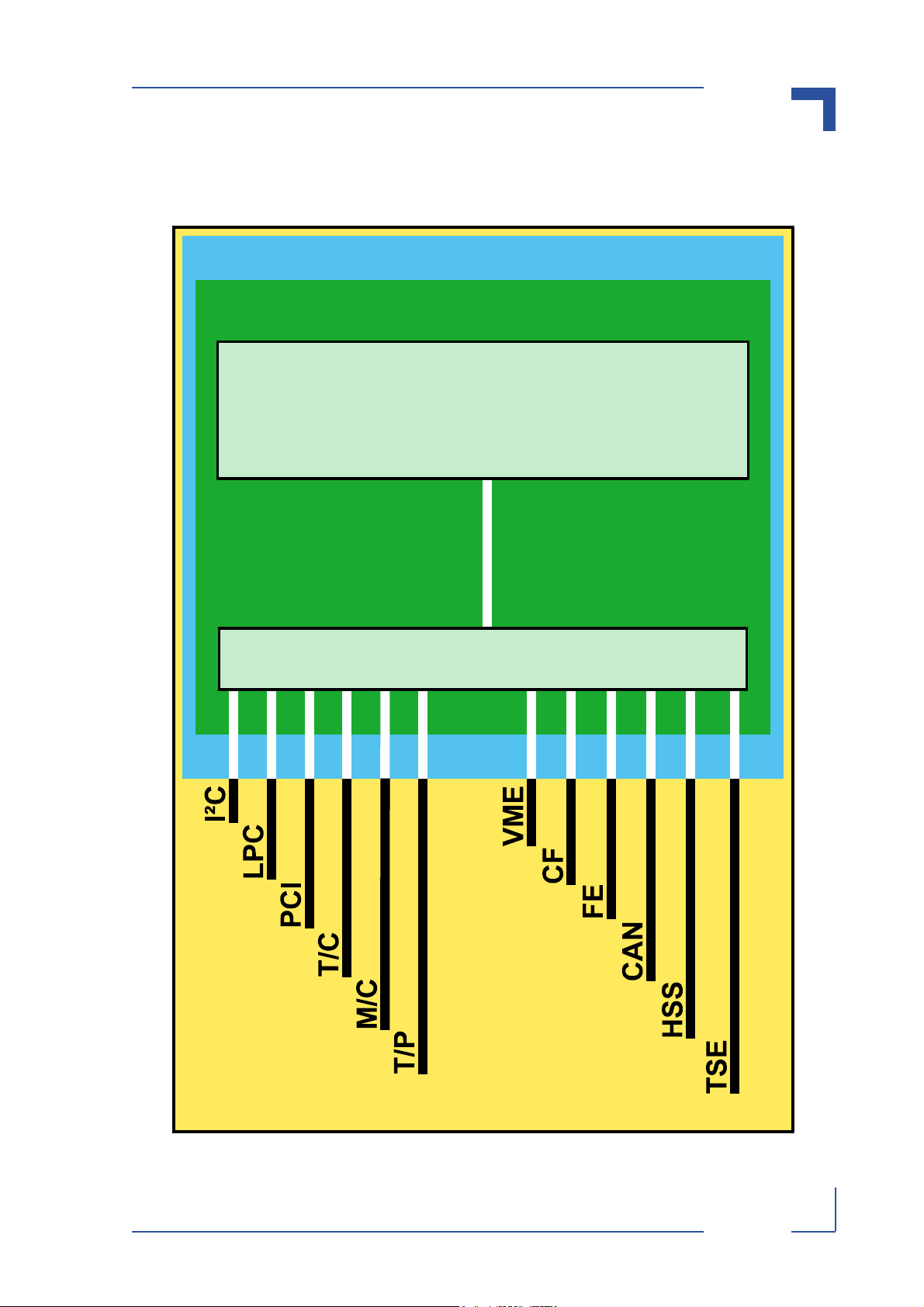
1.3 Board Diagrams
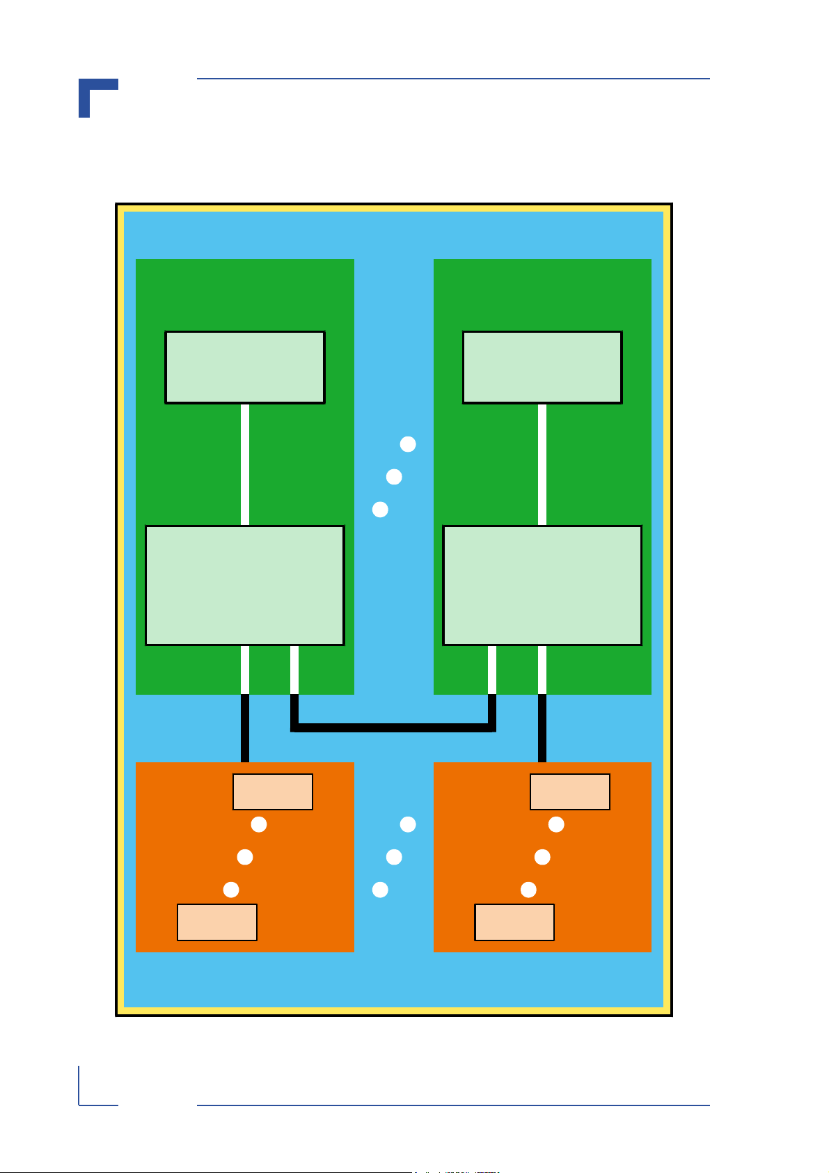
The following diagrams provide additional information concerning board functionality and component layout.
LEGEND FOR FIGURE 1-2:
CAN Communications Area Network
CF CompactFlash
FE Fast Ethernet
HSS High Speed Serial
I²C Inter-Integrated Circuit
LPC Low Pin Count
M/C Monitor and Control
PCI Peripheral Component Interface
T/C Terminal/Console (Serial Interface)
T/P Test/Programming
TSE Gigabit Ethernet (Three Speed Ethernet)
P R E L I M I N A R Y
29230.01.UG.VC.050727/091408
ID 29230, Rev. 01 © 2005 Kontron Modular Computers GmbH Page 1 - 5
Page 26
Introduction VMP3
1.3.1 Application System Interfacing
Figure 1-1: VMP3 Application System Interfacing Diagram
Application System (AS)
VMP3 VMP3
EB8541E
Board
Interfacing
P R E L I M I N A R Y
AS
Processes
EB8541E
Board
Interfacing
AS
Processes
Page 1 - 6 © 2005 Kontron Modular Computers GmbH ID 29230, Rev. 01
29230.01.UG.VC.050727/091408
Page 27
VMP3 Introduction
1.3.2 System Level Interfacing
Figure 1-2: VMP3 System Level Interfacing Diagram
VMP3 System
VMP3
EB8541E E²Brain Module
VMP3 Interfaces
P R E L I M I N A R Y
29230.01.UG.VC.050727/091408
ID 29230, Rev. 01 © 2005 Kontron Modular Computers GmbH Page 1 - 7
Page 28
Introduction VMP3
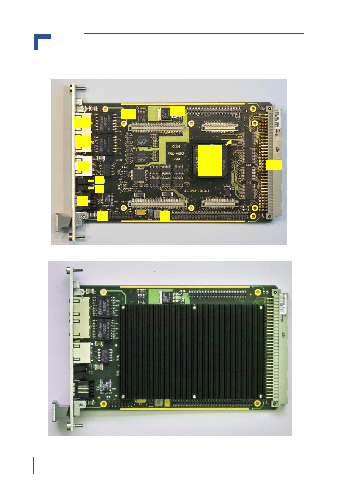
1.3.3 Board Layout
Figure 1-3: VMP3 Board (Front View Without E²Brain™ Module)
J12
J11
J5A
J5B
PCI
to
J6
D1
D2
VME
Bridge
J7
J8 J9
Figure 1-4: VMP3 Board (Front View With E²Brain™ Module)
J10
P R E L I M I N A R Y
Page 1 - 8 © 2005 Kontron Modular Computers GmbH ID 29230, Rev. 01
29230.01.UG.VC.050727/091408
Page 29
VMP3 Introduction
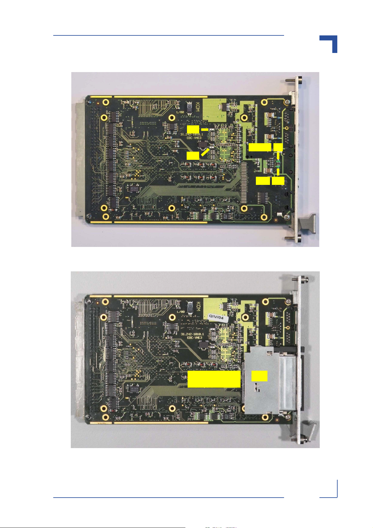
Figure 1-5: VMP3 Board (Rear View)
JP1
SPEED
JP2
Figure 1-6: VMP3 Board (Rear View with Optional CompactFlash Socket)
D7
D11ACT
29230.01.UG.VC.050727/091414
ID 29230, Rev. 01 © 2005 Kontron Modular Computers GmbH Page 1 - 9
CompactFlash
Socket
P R E L I M I N A R Y
J13
Page 30
Introduction VMP3
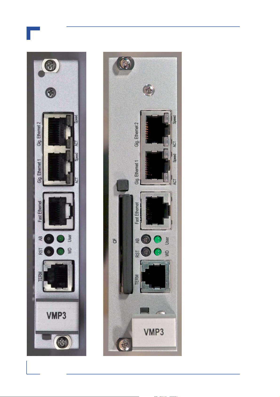
Figure 1-7: VMP3 Front Panels (4HP Standard and 6HP with CompactFlash)
P R E L I M I N A R Y
Page 1 - 10 © 2005 Kontron Modular Computers GmbH ID 29230, Rev. 01
29230.01.UG.VC.050727/091416
Page 31

VMP3 Introduction
1.4 Technical Specifications
Table 1-2: VMP3 Main Specifications
VMP3 Specifications
Processor Motorola MPC8541E Integrated Processor PowerPC, e500 core
Cache Structure 32 KB instruction cache and 32 KB data cache; L2 cache: 256 KB
On Chip Controllers Coherency Module, DDR-SDRAM, OCeaN switch fabric, Local Bus, FCC, TSEs,
Security Engine
Main Memory Soldered DDR-SDRAM: up to 256 MB, 64-bit, 264 MHz with ECC
Watchdog Watchdog generates exception condition: system reset, NMI, or cascading
RTC Real-time clock, backed up via VME auxiliary power (+5VSTDBY)
Processor and Related
BPCC E²Brain™ Board Process/Communications Controller: controls Local Bus
interfacing, provides LPC interface and monitor and control functions
SRAM 1 MB soldered, 512k x 16, optionally backed up via auxiliary power (+5VSTDBY)
EEPROM (I²C) 64 kBit soldered, serial access
Memory
Flash Minimum of 4 MB and up to 64 MB soldered
Peripheral
VME ANSI/VITA 1-1994 for VME, approved April 10.1995
Support for A24:D16/8 master and A24:D16/8 slave interface
PCI On-chip controller, 32-bit, 33 MHz, PCI System Master
LPC Low Pin Count sub-set, 8-bit IO and memory space access, realized in BPCC
I²C On-chip, message interface, full master/slave
CF CompactFlash, optional (PIO mode)
Fast Ethernet One 10baseT, 100baseTX, FCC integrated in MPC8541E, Intel PHY: LXT 972
Gigabit Ethernet Two three speed Ethernet (TSE): 10/100/1000 Mbit GMII (Marvell PHY: 88E1011)
CAN Controller Area Network interface (Philips SJA1000)
External Interfaces
Serial Ports Terminal and Console:
Two serial ports: RS232: TERM1 (Terminal on front panel)
TTL: TERM2 (Console on I/O expansion)
High Speed Serial:
Four ports, full modem : SER1 (on I/O expansion)
(Local Bus) : SER2 (on I/O expansion)
(Support for RS485 direction control) : SER3 (on I/O expansion)
: SER4 (on I/O expansion)
P R E L I M I N A R Y
JTAG/Debug JTAG/Debug interface for MPC8541E emulation probe
T/P
In-System
Programming
Interfaces
29230.01.UG.VC.050727/091419
ID 29230, Rev. 01 © 2005 Kontron Modular Computers GmbH Page 1 - 11
In-System-Programming interface for the VMP3 CPLD logic device
Page 32

Introduction VMP3
Table 1-2: VMP3 Main Specifications (Continued)
VMP3 Specifications
LEDs Six LEDs:
One general pupose (USER)
One Watchdog (WD)
M/C
Interfaces
Switches Two puch buttons: Reset and Abort
Connectors VME connector, 96-pin
Two Ethernet Activity/Link
Two Ethernet Speed
Onboard connectors: 1 x RJ12 for RS232; 2 x RJ45 for GigaEthernet; 1 x RJ45 for
Fast Ethernet
PCI expansion connector: Samtec FLE-150-01-G-DV
I/O expansion connector: Samtec FLE-136-01-G-DV
Power Consumption Source: 5 V: consumption: 10.85 watts @ 800 MHz (Ethernet not connected)
Temperature Range Operational: 0ºC to +60ºC Standard
-40ºC to +85ºC E2 (on request)
General
Climatic Humidity 93% relative humidity at 40°C, non-condensing
Dimensions 160 mm L x 100 mm W x 4HP H (minimum height)
Board Weight 300 g (4HP); 447 g (8HP)
Storage: -55ºC to +125ºC
The maximum height of the VMP3 is a function of the BrainCAP™ options as well
as the other possible optional interfaces.
P R E L I M I N A R Y
Page 1 - 12 © 2005 Kontron Modular Computers GmbH ID 29230, Rev. 01
29230.01.UG.VC.050727/091420
Page 33

VMP3 Introduction
1.5 Applied Standards
The Kontron Modular Computers’ VMP3 board complies with the requirements of the following
standards:
Table 1-3: Applied Standards
COMPLIANCE TYPE STANDARD TEST LEVEL
CE Emission EN55022
EN61000-6-3
Immission EN55024
EN61000-6-2
Electrical Safety EN60950 --
Mechanical Mechanical Dimensions IEEE 1101.10 --
Transport and Storage IEC 61131-2 --
Environmental and
Health Aspects
Vibration (sinusoidal) IEC60068-2-6 10 - 300 [Hz] / 5 [g] / 1 [oct / min]
Shock IEC60068-2-27 30 [g]
Bump IEC60068-2-29 15 [g]
--
--
10 [cycles / axis]
3 [axis: x, y, z]
9 [ms]
3 [shocks per direction]
5 [s] recovery time
6 [directions, ±x, ±y, ±z]
11 [ms]
500 [shocks per axis]
1 [s] recovery time
3 [axis: x, y, z]
29230.01.UG.VC.050727/091420
ID 29230, Rev. 01 © 2005 Kontron Modular Computers GmbH Page 1 - 13
Vibration, broad-band
random (digital control)
and guidance
Climatic Humidity IEC60068-2-78 93% RH at 40°C, non-condensing
IEC60068-2-64 20 - 2000 [Hz] / 3.5 [g RMS]
30 [min.] test time / axis
3 [axis: x, y, z]
P R E L I M I N A R Y
Page 34

Introduction VMP3
1.6 Related Publications
Table 1-4: Related Publications
ISSUED BY DOCUMENT
PCI PCI-SIG PCI Local Bus Specification, R.2.2
VME ANSI/VITA 1-1994 for VME
LPC Intel® Intel® Low Pin Count (LPC) Interface Specification,
Rev. 1.1
I²C Philips I2C-BUS SPECIFICATION, Rev. 2.1
E²Brain Kontron Modular Computers E²Brain™ Module Specification, Rev. 01
P R E L I M I N A R Y
Page 1 - 14 © 2005 Kontron Modular Computers GmbH ID 29230, Rev. 01
29230.01.UG.VC.050727/091420
Page 35

VMP3 Functional Description
Chapter 1
2
Functional Description
29230.01.UG.VC.050727/091420
ID 29230, Rev. 01 © 2005 Kontron Modular Computers GmbH Page 2 - 1
P R E L I M I N A R Y
Page 36

Functional Description VMP3
This page has been intentionally left blank.
P R E L I M I N A R Y
Page 2 - 2 © 2005 Kontron Modular Computers GmbH ID 29230, Rev. 01
29230.01.UG.VC.050727/091420
Page 37

VMP3 Functional Description
2. Functional Description
The following chapters present more detailed, board level information about the VMP3
E²Brain™ High Performance PowerPC Processor VME board whereby the board components
and their basic functionality are discussed in general.
2.1 General Information
The VMP3 is comprised basically of the EB8541 E²Brain™ module and the EBC-VME3 carrier
board.
The EB8541 E²Brain™ module consists of the following:
• a Motorola MPC8541E Integrated Processor, Power QUICC III with a PPC e500 core
• a Board Process/Communications Controller (BPCC)
• System and Communications interfacing to the EBC-VME3 for:
•I²C bus
• LPC bus
• PCI bus
• CompactFlash (CF) interface
• Terminal and Console (T/C) serial interfacing
• Monitor and Control (M/C) interfacing
• Test and Programming (T/P) interfacing
• High Speed Serial (HSS) communications
• Communications Area Network (CAN) bus
• Fast Ethernet (FE)
• Gigabit Ethernet (TSE)
• Memory elements:
• Main memory DDR-I-SDRAM, soldered
• Soldered SRAM, backed-up using an auxiliary power line
• Soldered FLASH
• Serial EEPROM
• a BrainCAP™ heat sink for the EB8541
• Software
• Operating system
• Board support package
• Boot strap loader (NetBootLoader)
P R E L I M I N A R Y
The EB8541 carrier board, EBC-VME3, consists of the following:
• a Tundra Universe II PCI-to-VME bridge and VME-bus connector for VME-bus system
interfacing
• PHYs, magnetics, and connectors for Gigabit Ethernet interfacing
• magnetics and connector for Fast Ethernet interfacing
• a Terminal connector for serial interfacing
• a PCI expansion connector for PCI peripheral interfacing
• an I/O expansion connector for additional system and communications interfacing
• two test and programming connectors for JTAG and ISP logic interfacing
• switches and LEDs for Monitor and Control interfacing
• an optional CompactFlash socket for Type I and II CF cards
29230.01.UG.VC.050727/091420
ID 29230, Rev. 01 © 2005 Kontron Modular Computers GmbH Page 2 - 3
Page 38

Functional Description VMP3
2.2 Board-Level Interfacing Diagram
The following figure demonstrates the interfacing structure between the internal processing elements of the EBC-VME3 and other major VMP3 module components. Where system elements have common interfacing they are grouped into a block. Interfacing common to only one
element of a block is indicated with a direct connecting line. The interfacing lines are shown in
white where they are on board and in black for board external interfacing.
LEGEND FOR FIGURE 2-1
AB Abort
ACT Activity
CAN Communications Area Network
CI Communications Interface
CIE Communications Interface Extension
CF CompactFlash
FE Fast Ethernet
HSS High Speed Serial
I²C Inter-Integrated Circuit
LPC Low Pin Count
MAG Magnetics
M/C Monitor/Control
PCI Peripheral Component Interface
PHY PHY
RST Reset
SI System Interface
SIE System Interface Extension
T/C Terminal/Console (Serial Interface)
T/P Test/Programming
P R E L I M I N A R Y
VME BUFs VME buffers
TSE Three Speed Ethernet
VME VME
WD Watchdog
Page 2 - 4 © 2005 Kontron Modular Computers GmbH ID 29230, Rev. 01
29230.01.UG.VC.050727/091420
Page 39

VMP3 Functional Description
Figure 2-1: VMP3 Board Level Interfacing
VMP3
EB8541 E²Brain Computer Core Module
SI
SI
PCI
PCI-BUS
PCI
-to-
VME
LPC
I²C
M/C
LED
USER
LED
VME
BUFs
WD
SW
AB
SW
RST
VME
J9
J11
J10 J7
M/C
CPLD
J12
ISP
M/C
T/C T/P
J8
CI
CI
MAG
J6
FE
LED
Activity
LED
Speed
CAN
HSS
J11
CIE
CIE
TSE1
PHY
LED
ACT
LED
Speed
MAG
J5B
TSE2
PHY
LED
ACT
LED
Speed
MAG
J5A
SIE
SIE
CF
* optional
*
J13
29230.01.UG.VC.050727/091420
ID 29230, Rev. 01 © 2005 Kontron Modular Computers GmbH Page 2 - 5
P R E L I M I N A R Y
Page 40

Functional Description VMP3
2.3 EB8541 E²Brain™ Module Interfaces
The following sections provide a very brief description of the interfacing between the E²Brain™
module and the EBC-VME3 board.
2.3.1 System Interface
As the name implies, this interface provides the basic application connection functionality required to integrate the EB8541 E²Brain™ module as the high performance core of the VMP3.
The System Interface is realized using a 140-pin, HIROSE FX8C-140P-SV connector. The following table provides an overview of the signal types and a brief description of the interfacing
realized on this connector.
Table 2-1: System Interface Signal Types
SIGNAL TYPE DESCRIPTION
POWER VMP3 E²Brain™ module input power, grounds, battery backup power, PCI
signaling voltage V(I/O)
MONITOR AND CONTROL (M/C) Control signals for E²Brain™ module operation, configuration, and addi-
tional GPIO interfacing
TEST AND PROGRAMMING (T/P) JTAG/Debug signals for Emulator interfacing
TERMINAL AND
CONSOLE (T/C)
I2C One I2C standard interface for low speed, serial, inter-chip communica-
LPC One LPC standard interface for (GP)IOs and simple memory interfacing
PCI One PCI standard interface for PCI-bus interfacing
Two 2-wire serial interfaces:
RxD1/TxD1: Used by the boot loader during startup as a terminal interface;
once the system has been booted, is available as general purpose serial interface (Terminal)
RxD2/TxD2: general purpose serial interface (Console)
tions
2.3.2 System Interface Extension
The System Interface Extension is realized using an 80-pin, HIROSE FX8C-80P-SV connector,
P R E L I M I N A R Y
and it is used to provide CPU architecture specific system interfaces.
In the case of the VMP3, a CompactFlash interface is made available on the System Interface
Extension.
Table 2-2: System Interface Extension Signal Types
SIGNAL TYPE DESCRIPTION
COMPACTFLASH One CompactFlash interface (true IDE mode)
POWER VMP3 E²Brain™ module input power and grounds
2.3.3 Communications Interface
The Communications Interface Connector is used to provide a set of standard communications
interfaces. In the case of the VMP3, there are three types of interfaces provided: four high
speed serial interfaces, one CAN interface, and one Fast Ethernet interface.
Page 2 - 6 © 2005 Kontron Modular Computers GmbH ID 29230, Rev. 01
29230.01.UG.VC.050727/091420
Page 41

VMP3 Functional Description
Table 2-3: Communications Interface Signal Types
SIGNAL TYPE DESCRIPTION
High Speed Serial (HSS) Four high speed serial interfaces
Fast Ethernet One Fast Ethernet 10/100 Mbps interface
CAN One standard CAN interface
2.3.4 Communications Interface Extension
The Communications Interface Extension is realized using a 140-pin, HIROSE FX8C-140P-SV
connector. The following table provides an overview of the signal types and a brief description
of the interfacing realized on this connector.
Table 2-4: Communications Interface Extension Signal Type
SIGNAL TYPE DESCRIPTION
GIGABIT ETHERNET Two Gigabit Ethernet interfaces (10/100/1000 Mbps, GMII)
29230.01.UG.VC.050727/091420
ID 29230, Rev. 01 © 2005 Kontron Modular Computers GmbH Page 2 - 7
P R E L I M I N A R Y
Page 42

Functional Description VMP3
2.4 VMP3 Board Interfaces
The following sections provide a specific information regarding the application interfaces available with the EBC-VME3 board.
2.4.1 J10 – VME Interface
The VME interface is based on the TUNDRA UNIVERSE II Bridge which includes the following
features required for 3U VME systems.
• A24/A16 addressing modes capability
• D16/D8 data transfer capability
• Automatic First-Slot-Detection
• Single level BR3 arbitration release-when-done
option
• FAIR VMEbus arbitration option
• ACFAIL NMI option
• SYSFAIL IRQ option
• System controller functions (SYSCLK, Bus
monitor, Power monitor)
• Compatibility with Kontron 3U VME system
addressing schemes
• Compatibility with Kontron VME backplane
design and feature set
• Compatibility with Kontron backplane transceiver
logic
The following figure and table provide pinout and signal
information for this interface.
Figure 2-2: J10 - VME Connector
PINROWS
C B A
1
P R E L I M I N A R Y
32
Page 2 - 8 © 2005 Kontron Modular Computers GmbH ID 29230, Rev. 01
29230.01.UG.VC.050727/091420
Page 43

VMP3 Functional Description
Table 2-5: Pinout of J10 Connector
PIN PINROW A PINROW B PINROW C
1 D00 BBSY D08
2 D01 BCLR D09
3D02 ACFAIL D10
4 D03 BG0IN D11
5 D04 BG0OUT D12
6 D05 BG1IN D13
7 D06 BG1OUT D14
8 D07 BG2IN D15
9 GND BG2OUT GND
10 SYSCLK BG3IN SYSFAIL
11 GND BG3OUT BERR
12 DS1 BR0 SYSRESET
13 DS0 BR1 LWORD
14 WRITE BR2 AM5
15 GND BR3 A23
16 DTACK AM0 A22
17 GND AM1 A21
18 AS AM2 A20
19 GND AM3 A19
20 IACK GND A18
21 IACKIN NC A17
22 IACKOUT NC A16
23 AM4 GND A15
24 A07 IRQ7 A14
25 A06 IRQ6 A13
26 A05 IRQ5 A12
27 A04 IRQ4 A11
28 A03 IRQ3 A10
29 A02 IRQ2 A09
30 A01 IRQ1 A08
31 -12V +5VSTDBY +12V
32 +5V +5V +5V
P R E L I M I N A R Y
29230.01.UG.VC.050727/091421
ID 29230, Rev. 01 © 2005 Kontron Modular Computers GmbH Page 2 - 9
Page 44

Functional Description VMP3
2.4.2 J5A/B – Dual Gigabit Ethernet Interface
This connector provides two three speed Ethernet (TSE1 and TSE2) interfaces (10/100/1000
mega-bit operation) for application communications interfacing. This is a dual RJ45 connector
with LEDs to indicate the status of the links.
The following figure and table provide pinout and signal information for this interface.
Figure 2-3: J5A/B - Dual Gigabit Ethernet Connector
LED OPERATION:
ACTSPEEDACTSPEED
J5A
J5B
TSE2 TSE1
8 1 8
Table 2-6: Pinouts of J5A and J5B Based on the Implementation
1
ACT OFF: link not active
GREEN: link active
GREEN BLINKING: activity on link
SPEED OFF: 10 Mbps
GREEN: 100 Mbps
YELLOW: 1000 Mbps
MDI / Standard Ethernet Cable
10BASE-T 100BASE-TX 1000BASE-T 10BASE-T 100BASE-TX 1000BASE-T
I/O SIGNAL I/O SIGNAL I/O SIGNAL I/O SIGNAL I/O SIGNAL I/O SIGNAL
O TX+ O TX+ I/O BI_DA+ 1 IRX+IRX+I/OBI_DB+
O TX- O TX- I/O BI_DA- 2 I RX- I RX- I/O BI_DB-
I RX+ I RX+ I/O BI_DB+ 3 O TX+ O TX+ I/O BI_DA+
----I/OBI_DC+4 ----I/OBI_DD+
----I/OBI_DC-5 ----I/OBI_DD-
I RX- I RX- I/O BI_DB- 6 O TX- O TX- I/O BI_DA-
----I/OBI_DD+7 ----I/OBI_DC+
----I/OBI_DD-8 ----I/OBI_DC-
Note ...
The Gigabit PHYs on the VMP3 support automatic MDI/MDIX crossover at all
P R E L I M I N A R Y
speeds of operation. Therefore both standard as well as crossed Ethernet
cables can be used with these interfaces.
PIN
MDIX / Crossed Ethernet Cable
Page 2 - 10 © 2005 Kontron Modular Computers GmbH ID 29230, Rev. 01
29230.01.UG.VC.050727/091422
Page 45

VMP3 Functional Description
2.4.3 J6 – Fast Ethernet Interface
This connector provides a single Fast Ethernet interface (10/100 mega-bit operation) for application communications interfacing. This is a single RJ45 connector without link status LEDs.
Link status LEDs for this interface are located on the bottom side of the EBC-VME3 board.
The following figure and table provide pinout and signal information for this interface.
Figure 2-4: J6 - Fast Ethernet Connector
LED OPERATION:
Speed
Activity
8 1
Table 2-7: Pinout of J6
Activity OFF: link not active
GREEN: link active
GREEN BLINKING: activity on link
Speed OFF: 10 Mbps
GREEN: 100 Mbps
PIN SIGNAL DESCRIPTION
1 TX+ Transmit data +
2 TX- Transmit data -
3 RX+ Receive data +
4 Terminated Bob-Smith termination
5 Terminated Bob-Smith termination
6 RX- Receive data -
7 Terminated Bob-Smith termination
9 Terminated Bob-Smith termination
P R E L I M I N A R Y
29230.01.UG.VC.050727/091422
ID 29230, Rev. 01 © 2005 Kontron Modular Computers GmbH Page 2 - 11
Page 46

Functional Description VMP3
2.4.4 J7 Terminal Interface
The VMP3 provides one serial interface for supporting a terminal port (TERM1). This interface
is realized using one of the MPC8541E on-chip UARTs, and as such provides only a two wire
interface without hardware handshake signals.
The connector J7 provides interfacing to the TERM1 port. This port can also be used as a low
speed solution for firmware updating. The signal levels on this connector are RS232 compliant.
The UART itself is a 16550 type UART.
The following figure and table provide pinout and signal information for the TERM1 interface.
Figure 2-5: J7 - TERM Connector
6 1
Table 2-8: Pinout of J7
PIN SIGNAL
1NC
2GND
3TxD1
4RxD1
5NC
6NC
P R E L I M I N A R Y
Page 2 - 12 © 2005 Kontron Modular Computers GmbH ID 29230, Rev. 01
29230.01.UG.VC.050727/091423
Page 47

VMP3 Functional Description
2.4.5 J8 JTAG/Debug Interface
This Test and Programming interface supports JTAG/Debug operations. This interface can be
used for connecting hardware emulators and debuggers (e.g. BDM, COP, …). It is comprised
of a set of ten signals whereby some are common to both interfaces and some are dedicated
to only one.
The following figure and tables provide pinout and signal information for this connector.
Figure 2-6: J8 - JTAG/Debug Connector
15
1
216
Table 2-9: Pinout of J8
SIGNAL PIN PIN SIGNAL
TDO 1 2 NC
TDI 3 4 TRST
(pulled to +3.3V with 10 kΩ)56EMU_VCC
TCK 7 8 CHKSTP_IN (pulled to +3.3V with 10 kΩ)
TMS 9 10 NC
SRST 11 12 NC
HRST 13 14 NC
CHKSTP_OUT (pulled to +3.3V with 10 kΩ)15 16GND
Table 2-10: JTAG/Debug Signal Descriptions
TCK Test Clock in for JTAG and emulator/debugger
TDI Test Data In for JTAG and emulator/debugger
TDO Test Data Out JTAG and emulator/debugger
TMS Test Mode Select, input for JTAG and emulator/debugger
TRST Test Reset, input for JTAG and emulator/debugger
HRST Hard Reset, emulator/debugger hard reset input
SRST Soft Reset, emulator/debugger reset input
CHKSTP_IN Checkstop input
CHKSTP_OUT Checkstop output
EMU_VCC Reference Voltage of the JTAG/DEBUG core
29230.01.UG.VC.050727/091424
ID 29230, Rev. 01 © 2005 Kontron Modular Computers GmbH Page 2 - 13
SIGNAL DESCRIPTION
P R E L I M I N A R Y
Page 48

Functional Description VMP3
2.4.6 J9 PCI Expansion Interface
The PCI Expansion connector provides the possibility to mount several transition boards above
the VMP3 for adding special functionality which is not provided on the VMP3 main board or on
the VME bus. All the PCI signals of the onboard PCI bus are routed to this connector, so that
a complete PCI bus is provided on this connector. In addition, almost the same number of
ground and power pins (3.3V and 5V) as are on a PCI or PMC connector are provided.
Examples of transition boards are:
• PMC carrier
• IO board with Graphic interface, SCSI, etc.
Figure 2-7: J9 PCI Expansion Connector
1 99
P R E L I M I N A R Y
1002
Page 2 - 14 © 2005 Kontron Modular Computers GmbH ID 29230, Rev. 01
29230.01.UG.VC.050727/091424
Page 49

VMP3 Functional Description
Table 2-11: Pinout of J9
SIGNAL PIN PIN SIGNAL SIGNAL PIN PIN SIGNAL
GND 1 2 SCL (I2C) AD17 51 52 AD16
RST# 3 4 +3.3V C/BE2 53 54 +5V
+3.3V 5 6 CLK1 GND 55 56 FRAME#
CLK2 7 8 GND IRDY# 57 58 GND
GND 9 10 NC +3.3V 59 60 TRDY#
INTB# 11 12 INTA# DEVSEL# 61 62 NC
INTD# 13 14 INTC# GND 63 64 STOP#
+5V 15 16 GNT1# LOCK# 65 66 +3.3V
GNT2# 17 18 +5V PERR# 67 68 +5V
+3.3V 19 20 NC SERR# 69 70 GND
GND 21 22REQ1# +5V 71 72PAR
REQ2# 23 24 GND C/BE1 73 74 AD15
+5V 25 26NC AD14 75 76+3.3V
AD31 27 28 AD30 GND 77 78 AD13
AD29 29 30 +5V AD12 79 80 AD11
GND 31 32AD28 AD10 81 82GND
AD27 33 34 AD26 GND 83 84 AD9
AD25 35 36 GND AD8 85 86 C/BE0
+3.3V 37 38 AD24 AD7 87 88 +5V
C/BE3 39 40 SDA (I2C) +3.3V 89 90 AD6
AD23 41 42 +3.3V AD5 91 92 AD4
GND 43 44 AD22 AD3 93 94 GND
AD21 45 46 AD20 NC 95 96 AD2
AD19 47 48 GND AD1 97 98 AD0
+5V 49 50 AD18 +12V 99 100 -12V
P R E L I M I N A R Y
29230.01.UG.VC.050727/091425
ID 29230, Rev. 01 © 2005 Kontron Modular Computers GmbH Page 2 - 15
Note...
The PCI signalling voltage is 5V on this connector.
Page 50

Functional Description VMP3
2.4.7 J11 I/O Expansion Interface
The I/O Expansion connector provides additional capability for LPC, TERM2, M/C, CAN, and
HSS/UART interfacing. All signals on this connector are at TTL levels which means that they
will require additional signal conditioning prior to interfacing to VMP3 external devices.
Figure 2-8: J11 I/O Expansion Connector
72
2
71 1
Table 2-12: Pinout of J11
SIGNAL PIN PIN SIGNAL SIGNAL PIN PIN SIGNAL
+BAT (see Note) 1 2 GND SER4_RI 37 38 SER4_RTS
MC4 3 4 LPC_CLK SER3_CD 39 40 SER4_DSR
LAD1 5 6 +3V3 SER3_RXD 41 42 GND
+5V 7 8 LAD0 SER3_CTS 43 44 SER3_DTR
LAD3 9 10 LAD2 SER3_RI 45 46 SER3_TXD
PCI_RST 11 12 GND +3V3 47 48 SER3_RTS
TXD2 13 14 LFRAME SER2_CD 49 50 SER3_DSR
RXD2 15 16 +5V SER2_RXD 51 52 GND
GND 17 18 SERIRQ GND 53 54 SER2_DTR
CAN1_RX1 19 20 +3V3 SER2_CTS 55 56 SER2_TXD
CAN1_RX0 21 22 CAN1_TX1 SER2_RI 57 58 SER2_RTS
GND 23 24 CAN1_TX0 +5V 59 60 SER2_DSR
P R E L I M I N A R Y
CAN2_RX1 25 26 +5V SER1_CD 61 62 +3V3
CAN2_RX0 27 28 CAN2_TX1 SER1_RXD 63 64 SER1_DTR
GND 29 30 CAN2_TX0 GND 65 66 SER1_TXD
SER4_CD 31 32 GND SER1_CTS 67 68 SER1_RTS
SER4_RXD 33 34 SER4_DTR SER1_RI 69 70 SER1_DSR
SER4_CTS 35 36 SER4_TXD +3V3 71 72 +5V
Note...
+BAT = 3.2V is derived from the 5V standby (is not regulated)
Page 2 - 16 © 2005 Kontron Modular Computers GmbH ID 29230, Rev. 01
29230.01.UG.VC.050727/091425
Page 51

VMP3 Functional Description
2.4.7.1 LPC Interface
One Low Pin Count (LPC) interface for supporting simple IOs, simple static memory devices,
and IO controllers is available via the I/O Expansion interface.
The controller is completely integrated in the BPCC and offers a 8-bit data access port to devices which use LPC IO or memory access protocols. I/O and memory area are selected using
different address spaces.
The I/O address space is 64 kByte in size, whereas the memory area offers 16 MByte address
space. DMA is not supported by this interface.
In addition, a serial IRQ controller is also implemented in the BPCC, controlling and collecting
the serial LPC IRQs and converting and processing them to IRQs for the CPU.
The serial IRQ controller is realized according to the “Serialized IRQ Support for PCI Systems”
Specification, Rev. 6.0, Sept. 1, 1995
The following table provides a listing of the LPC interface signals and a brief description.
Table 2-13: LPC Interface Signal Description
SIGNAL DESCRIPTION
LAD[0:3] Multiplexed Command, Address, and Data lines
LFRAME# Indicates start of a new cycle, termination of broken cycle
LPCCLK 33 MHz clock
SERIRQ Serialized IRQ, optional for peripherals that need interrupt
2.4.7.2 Terminal Interface
A second serial interface for supporting a terminal port and a low speed communications interface (TERM2) for firmware updating is provided on this connector. This interface is realized using one of the MPC8541E on-chip UARTs, and, as such, provides only a two wire interface
without hardware handshake signals.
Note...
The corresponding serial signals on the VMP3 are TTL logic level signals.
Therefore, the transceivers for RS232 must be provided by the carrier board.
WARNING!
The signal level on the receive lines must not exceed 3.3V. Transients and signal levels higher than 3.3V may damage the VMP3 board.
P R E L I M I N A R Y
29230.01.UG.VC.050727/091426
ID 29230, Rev. 01 © 2005 Kontron Modular Computers GmbH Page 2 - 17
Page 52

Functional Description VMP3
2.4.7.3 CAN Interface
To provide field bus support, there are signals available to implement a CAN bus interface
(Philips SJA 1000) via the J11 connector. The signals provided are at 5V TTL voltage levels
and must be adapted to the CAN bus levels through the use of appropriate CAN transceivers
on the carrier board.
Table 2-14: CAN Interface Signal Type and Description
SIGNAL DESCRIPTION
CAN1_TX[0:1] Transmit data output driver
CAN1_RX[0:1] Receive data input channel
Note...
For more information concerning interfacing of the SJA 1000 to the CAN PHY,
refer to the Philips Application Note: AN97076 or the datasheet of the PCA
82C250 CAN controller interface.
2.4.7.4 High Speed Serial Interfaces
Four, full modem, serial ports (SER1, 2, 3, and 4) are available on the I/O expansion connector.
Eight signals per port are provided to realize asynchronous high speed serial links interfaced
using dedicated controlling/handshaking. The VMP3 uses DUARTs (EXAR XR 16C2850 or
XR16L2750) which are 16550 compatible and provide hardware handshaking support for
RS485 operation.
Table 2-15: High Speed Serial Interface Signal Type and Description
SIGNAL DESCRIPTION
SERn_TXD Transmit data output
SERn_RXD Receive data input
SERn_RTS Request to send output
P R E L I M I N A R Y
SERn_CTS Clear to send input
SERn_DTR Data terminal ready output
SERn_CD Carrier detect input
SERn_DSR Data set ready input
SERn_RI Ring indicator input
Note...
All signals are available and supplied at 3.3V TTL levels. Further signal conditioning via appropriate transceivers on the carrier board is required to support
the respective communications standards.
Page 2 - 18 © 2005 Kontron Modular Computers GmbH ID 29230, Rev. 01
29230.01.UG.VC.050727/091426
Page 53

VMP3 Functional Description
2.4.7.5 Monitor and Control Interfaces
The I/O expansion connector provides one MC signal: the MC4 which is an input and is used
as a
boot control signal. Low = boot from LPC device; high or open = boot from onboard
FLASH.
2.4.8 J12 In-System-Programming Interface
This programming interface supports in-system-programming of the VMP3 CPLD logic device.
The following figure and table provide pinout and signal information for this connector.
Figure 2-9: J12 In-System-Programming Connector
9
10
Table 2-16: Pinout of J12
SIGNAL PIN PIN SIGNAL
L_TCK 1 2 GND
L_TDO 3 4 +3V3
L_TMS 5 6 NC
NC 7 8 NC
L_TDI 9 10 GND
1
2
P R E L I M I N A R Y
29230.01.UG.VC.050727/091426
ID 29230, Rev. 01 © 2005 Kontron Modular Computers GmbH Page 2 - 19
Page 54

Functional Description VMP3
This page has been intentionally left blank.
P R E L I M I N A R Y
Page 2 - 20 © 2005 Kontron Modular Computers GmbH ID 29230, Rev. 01
29230.01.UG.VC.050727/091427
Page 55

VMP3 Installation
Chapter 1
3
Installation
29230.01.UG.VC.050727/091427
ID 29230, Rev. 01 © 2005 Kontron Modular Computers GmbH Page 3 - 1
P R E L I M I N A R Y
Page 56

Installation VMP3
This page has been intentionally left blank.
P R E L I M I N A R Y
Page 3 - 2 © 2005 Kontron Modular Computers GmbH ID 29230, Rev. 01
29230.01.UG.VC.050727/091427
Page 57

VMP3 Installation
3. Installation
The VMP3 has been designed for easy installation. However, the following standard precautions, installation procedures, and general information must be observed to ensure proper installation and to preclude damage to the board or injury to personnel.
3.1 Hardware Installation
The product described in this manual can be installed in any available slot of a VMEbus system.
However, to function as a system controller it must be installed in slot 1 (far left).
3.1.1 Safety Requirements
The module must be securely fastened to the carrier board using the mounting standoffs and
screws provided with the module.
In addition the following electrical hazard precautions must be observed.
Caution, Electric Shock Hazard!
Ensure that the system main power is removed prior to installing or removing
this board. Ensure that there are no other external voltages or signals being
applied to this board or other boards within the system. Failure to comply with
the above could endanger your life or health and may cause damage to this
board or other system components including process-side signal conditioning
equipment.
ESD Equipment!
This Kontron board contains electrostatic sensitive devices. Please observe
the following precautions to avoid damage to your board:
Discharge your clothing before touching the assembly. Tools must be discharged before use.
Do not touch any on board components, connector pins, or board conductive
circuits.
If working at an anti-static workbench with professional discharging equipment, ensure compliance with its usage when handling this product.
P R E L I M I N A R Y
29230.01.UG.VC.050727/091427
ID 29230, Rev. 01 © 2005 Kontron Modular Computers GmbH Page 3 - 3
Page 58

Installation VMP3
3.1.2 Installation Procedures
To install the board proceed as follows:
1. Ensure that the safety requirements indicated above are observed.
Warning!
Failure to comply with the instruction below may cause damage to the
board or result in improper system operation. Please refer to chapter 4 for
configuration information.
2. Ensure that the board is properly configured for operation before installing.
Note...
Care must be taken when applying the procedures below to ensure that
when the board is inserted it is not damaged through contact with other
boards in the system.
3. Install the board in the appropriate slot and ensure that it is properly seated in the backplane (front panel is flush with the rack front).
4. Fasten the front panel retaining screws.
5. Connect external interfacing cables to the board as required.
6. Ensure that the board and interfacing cables are properly secured.
3.1.3 Removal Procedures
To remove the board proceed as follows:
1. Ensure that the safety requirements indicated above are observed.
Warning!
Care must be taken when applying the procedures below to ensure that
when the board is removed it is not damaged through contact with other
boards in the system. This applies in particular when complementary
P R E L I M I N A R Y
2. Disconnect any interfacing cables that may be connected to the board.
3. Loosen the front panel retaining screws.
boards are connected to the VMP3 via the J9 or J11 connectors. In this
case, both boards must be removed together as a unit and not separately.
4. Disengage the board from the backplane by pressing down on the front panel handle and
pull the board out of the slot.
5. Dispose of the module as required observing applicable environmental regulations governing the handling and disposition of this type of product.
Page 3 - 4 © 2005 Kontron Modular Computers GmbH ID 29230, Rev. 01
29230.01.UG.VC.050727/091427
Page 59

VMP3 Installation
Note...
If the removed board is to be returned to the manufacturer, ensure that
the packaging and ESD requirements are observed as specified by the
following sections of this guide:
• page xv, "Special Handling and Unpacking Instructions"
• page xvi, "General Instructions on Usage"
• section 1.8, "Applied Standards"
3.2 Software Installation
Software installation is a function of the NetBootLoader and is described in chapter 5 of this
manual.
29230.01.UG.VC.050727/091427
ID 29230, Rev. 01 © 2005 Kontron Modular Computers GmbH Page 3 - 5
P R E L I M I N A R Y
Page 60

Installation VMP3
This page has been intentionally left blank.
P R E L I M I N A R Y
Page 3 - 6 © 2005 Kontron Modular Computers GmbH ID 29230, Rev. 01
29230.01.UG.VC.050727/091427
Page 61

VMP3 Configuration
Chapter 1
4
Configuration
29230.01.UG.VC.050727/091434
ID 29230, Rev. 01 © 2005 Kontron Modular Computers GmbH Page 4 - 1
P R E L I M I N A R Y
Page 62

Configuration VMP3
This page has been intentionally left blank.
P R E L I M I N A R Y
Page 4 - 2 © 2005 Kontron Modular Computers GmbH ID 29230, Rev. 01
29230.01.UG.VC.050727/091434
Page 63

VMP3 Configuration
4. Configuration
The following sections provide system integrators with detailed information for configuring the
VMP3 module for operation
4.1 Board Address Map
The following table illustrates the address mapping of the VMP3.
Table 4-1: Board Address Map
AREA
NAME
ROM/REGs/
UARTs
CAN 32 k 0xFFFF 0000 0xFFFF C000 Reserved
CF 64 k 0xFFFE 0000 0xFFFF A014 Delay Timer Control/Status R/W
Reserved 896 k 0xFFF0 0000 0xFFFF A013 Device Disable Register R
MPC8541E
REGs
Reserved 2 M 0xFFC0 0000 0xFFFF A010 Serial Interrupt Polarity1 R/W
SRAM 4 M 0xFF80 0000 0xFFFF A00F Serial Interrupt Mask 2 Register R/W
O V E R L A P
Reserved 8 M 0xFF00 0000 0xFFFF A00E Serial Interrupt Mask 1 Register R/W
LPC IO 16 M 0xFE00 0000 0xFFFF A00D Serial Interrupt 2 Pending R/W
LPC MEM 16 M 0xFD00 0000 0xFFFF A00C Serial Interrupt 1 Pending R/W
Reserved 16 M 0xFC00 0000 0xFFFF A00B Reserved R/W
FLASH 64 M 0xF800 0000 0xFFFF A00A Reserved R
PCI 2 G 0x9000 0000 0xFFFF A009 Board/Logic Revision R/W
VME 256 M 0x8000 0000 0xFFFF A008 Watchdog Control Register R/W
SIZE
BYTE
32 k 0xFFFF 8000 0xFFFF E000 ROM R
1 M 0xFFE0 0000 0xFFFF A011 Serial Interrupt Polarity2 R/W
START
ADDRESS
START
ADDRESS
REGISTER
NAME
ACC.
DDR-SRAM 2 G 0x0000 0000 0xFFFF A007 Reserved
29230.01.UG.VC.050727/091434
ID 29230, Rev. 01 © 2005 Kontron Modular Computers GmbH Page 4 - 3
0xFFFF A006 Device Interrupt Pending R/W
0xFFFF A005 Interrupt Config Register R/W
0xFFFF A004 Event Register R/W
0xFFFF A003 Control Register R/W
0xFFFF A002 Memory Configuration Register R
0xFFFF A001 Software Compatibility ID R
0xFFFF A000 Board ID R
0xFFFF 8018 UART_D R/W
0xFFFF 8010 UART_C R/W
0xFFFF 8008 UART_B R/W
0xFFFF 8000 UART_A R/W
P R E L I M I N A R Y
Page 64

Configuration VMP3
4.2 Board Control Registers
The Board Control registers may be accessed through byte-wide read and write operations.
4.2.1 Board ID Register
The Board ID is used to identify the VMP3 in a E²Brain™ system. The value for the VMP3 is
0x45 which is factory set and cannot be changed.
Table 4-2: Board ID Register
REGISTER NAME BOARD ID ACCESS
ADDRESS 0xFFFF A000 R
BIT POSITION
CONTENT BID7 BID6 BID5 BID4 BID3 BID2 BID1 BID0
DEFAULT 01000101
7 6 5 4 3 2 1 0
MSB
4.2.2 Software Compatibility ID
The Software Compatibility ID will signal to the software when differences in hardware require
different handling by the software. It starts with the value 0x00 and will be incremented with
each change in hardware (software sensitive only). This register is set at the factory and is for
use only by the boot strap loader “NetBootLoader” and the BSP software, and, as such, is not
user relevant.
Table 4-3: Software Compatibility ID
REGISTER NAME SOFTWARE COMPATIBILITY ID ACCESS
ADDRESS 0xFFFF A001 R
BIT POSITION
CONTENT SC7 SC6 SC5 SC4 SC3 SC2 SC1 SC0
DEFAULT n/a n/a n/a n/a n/a n/a n/a n/a
7 6 5 4 3 2 1 0
MSB
P R E L I M I N A R Y
LSB
LSB
Page 4 - 4 © 2005 Kontron Modular Computers GmbH ID 29230, Rev. 01
29230.01.UG.VC.050727/091434
Page 65

VMP3 Configuration
4.2.3 Memory Configuration Register
The memory configuration register provides information concerning SDRAM size, ECC, and
memory bus clock.
Table 4-4: Memory Configuration Register
REGISTER NAME MEMORY CONFIGURATION ACCESS
ADDRESS 0xFFFF A002 R W
BIT POSITION
CONTENT res.
7 6 5 4 3 2 1 0
MSB
SYS_
CLK
MEM
BUS
CLOCK
ECC res.
MEM_
SZ1
MEM_
SZ0
DEFAULT n/a 0 1 0 n/a n/a n/a n/a
BIT CONTENT STATE DESCRIPTION
0
0 reserved
1
Memory size:
0
1MEM_SZ0
1
0
2MEM_SZ1
1
Bit 2 Bit 1
0 0 128 MB (256 Mbit chips)
0 1 256 MB (512 Mbit chips)
1 0 512 MB (1 Gbit chips)
11 reserved
0
3 reserved
1
ECC not available
0
4ECC
ECC available
1
LSB
res.
MEM BUS
5
CLOCK
SYS_CLK
6
reserved
7
29230.01.UG.VC.050727/091435
ID 29230, Rev. 01 © 2005 Kontron Modular Computers GmbH Page 4 - 5
264 MHz (Maximum possible memory bus clock)
0
330 MHz (Maximum possible memory bus clock)
1
0 = 33 MHz; 1 = 66 MHz
0
This information is required in order to configure the PLL settings inside
1
the SOC.
0
1
P R E L I M I N A R Y
Page 66

Configuration VMP3
4.2.4 Control Register
The Control register provides output interfacing to the application software. Assertion of the appropriate bits by the application software will cause the BPCC to generate outputs accordingly.
During startup, the state of Bit 0 is controlled by the NetBootLoader software. After the startup
is completed, the NetBootLoader sets Bit 0 to 1.
Table 4-5: Control Register
REGISTER NAME CONTROL ACCESS
ADDRESS 0xFFFF A003 R W
BIT POSITION
CONTENT res. res. MC10 S_RST MC9 res. MC11 MC6
DEFAULT n/an/a0n/a0n/a0n/a
BIT CONTENT STATE DESCRIPTION
0MC6
1MC11
2 reserved
3MC9
4S_RST
5MC10
7 6 5 4 3 2 1 0
MSB
Logical high on the MC6 output pin
0
Logical low on the MC6 output pin
1
Logical high on the MC11 output pin
0
Logical low on the MC11 output pin
1
0
1
Logical low on the MC9 output pin
0
High impedance (Z) on the MC9 output pin
1
no operation
0
Causes a complete system reset (S_RST) to be initiated
1
Logical low on the MC10 output pin
0
High impedance (Z) on the MC10 output pin
1
LSB
P R E L I M I N A R Y
6 reserved
7 reserved
0
1
0
1
4.2.5 Event Register
The Event register provides status information about the Watchdog timer and various monitor
and control inputs. Depending on the type of event which occurs, interrupts may be generated
automatically which then require servicing. The application software is responsible for servicing
the interrupts as well as the other events, and, where applicable, the resetting of the event bits.
Page 4 - 6 © 2005 Kontron Modular Computers GmbH ID 29230, Rev. 01
29230.01.UG.VC.050727/091435
Page 67

VMP3 Configuration
Table 4-6: Event Register
REGISTER NAME EVENT ACCESS
ADDRESS 0xFFFF A004 R W
BIT POSITION
7 6 5 4 3 2 1 0
MSB
CONTENT MC5 MC3 res. MC2 MC8 MC1 ALARM res.
DEFAULT n/a n/a n/a n/a n/a 0 0 n/a
BIT CONTENT STATE DESCRIPTION
0
0 reserved
1
Indicates that ALARM signal on RTC has not been asserted
0
1ALARM
Indicates that ALARM signal on RTC has been asserted
1
Indicates that the MC1 signal has not been asserted
0
2MC1
Indicates that the MC1 signal has been asserted
(This will result in a NMI being generated which can be cleared by writing a
1
’1’.)
Indicates that the EB405 is being operated in Agent mode
0
3MC8
1
Indicates that the EB405 is being operated in Master mode
Case: MC2_INT_EN = 0
Indicates the status of the MC2 input: electrical: low = 0, high = 1
0
4MC2
Case: MC2_INT_EN = 1 (default = 0)
The falling edge of the signal on MC2 pin sets this bit to ’1’ and generates
the MCInt on the CPU provided it is enabled there
1
(This may be cleared by writing a ’1’.)
LSB
5 reserved
6MC3
7MC5
29230.01.UG.VC.050727/091435
ID 29230, Rev. 01 © 2005 Kontron Modular Computers GmbH Page 4 - 7
0
1
Case: MC3_INT_EN = 0
Indicates the status of the MC3 input: electrical: low = 0, high = 1
0
Case: MC3_INT_EN = 1 (default = 0)
The falling edge of the signal on MC3 pin sets this bit to ’1’ and generates
the MCInt on the CPU provided it is enabled there
1
(This may be cleared by writing a ’1’.)
Case: MC3_INT_EN = 0
Indicates the status of the MC3 input: electrical: low = 0, high = 1
0
Case: MC3_INT_EN = 1 (default = 0)
The falling edge of the signal on MC3 pin sets this bit to ’1’ and generates
the MCInt on the CPU provided it is enabled there
1
(This may be cleared by writing a ’1’.)
P R E L I M I N A R Y
Page 68

Configuration VMP3
4.2.6 Interrupt Configuration Register
The interrupt configuration register acts as an interrupt enable register for the MC2, MC3 and
MC5 signals.
Table 4-7: Interrupt Configuration Register
REGISTER NAME INTERRUPT CONFIGURATION ACCESS
ADDRESS 0xFFFF A005 R W
BIT POSITION
CONTENT
DEFAULT
7 6 5 4 3 2 1 0
MSB
MC5_INT_ENMC3_INT_
EN
0 0 n/a 0 n/a n/a n/a n/a
res.
MC2_INT_
EN
res. res. res. res.
BIT CONTENT STATE DESCRIPTION
0
0 reserved
1
0
1 reserved
1
0
2 reserved
1
0
3 reserved
1
Disabled
0
4 MC2_INT_EN
Enabled
1
0
5 reserved
1
LSB
Disabled
P R E L I M I N A R Y
6 MC3_INT_EN
0
Enabled
1
Disabled
0
7 MC5_INT_EN
Enabled
1
4.2.7 Device Interrupt Pending Register
The Device Interrupt Pending Register is used to identify the source of the pending interrupt
request of the following onboard devices:
• Temperature sensor (TEMP)
• Fast Ethernet PHY interrupt (FCC1 and FCC2)
• UARTs (SER1, SER2, SER3, and SER4)
Page 4 - 8 © 2005 Kontron Modular Computers GmbH ID 29230, Rev. 01
29230.01.UG.VC.050727/091435
Page 69

VMP3 Configuration
Table 4-8: Device Interrupt Pending Register
REGISTER NAME DEVICE INTERRUPT PENDING ACCESS
ADDRESS 0xFFFF A006 R
BIT POSITION
CONTENT res. TEMP FCC2 FCC1 SER4 SER3 SER2 SER1
DEFAULT 00000000
For information regarding the required hardware resources, refer to chapter “Interrupt
Mapping” in this manual. A logical ’1’ indicates that an interrupt has been asserted.
7 6 5 4 3 2 1 0
MSB
LSB
4.2.8 Watchdog Control Register
The Watchdog Control register is the interface between applications and the operating system
for controlling the functioning of the Watchdog timer. There are four possible modes of operation involving the Watchdog timer:
• Timer only
• Reset
• Interrupt
• Dual stage
At power on the Watchdog is not enabled. If not required, it is not necessary to enable it. If required, the bits of the Watchdog Control register must be set according to application requirements. To operate the Watchdog, the mode and time period required must first be set and then
the Watchdog enabled. Once enabled, the Watchdog can only be disabled or the mode
changed by powering down and then up again. To prevent a Watchdog timeout the Watchdog
must be retriggered before timing out. This is done by writing a ’1’ to the WTR bit. In the event
a Watchdog timeout does occur, the WTE bit is set to ’1’. What transpires after this depends on
the mode selected. The four operational Watchdog timer modes are described as follows.
Timer only - In this mode the Watchdog is enabled using the required timeout period. Normally
the Watchdog is retriggered by writing a ’1’ to the WTR bit. In the event a timeout occurs, the
WTE bit is set to ’1’. This bit can then be polled by the application and handled accordingly. To
continue using the Watchdog, write a ’1’ to the WTE bit, and then retrigger the Watchdog using
WTR. The WTE bit retains its setting as long as no power down-up is done. Therefore, this bit
may be used to verify the status of the Watchdog.
Reset mode - This mode is used to force a hard reset in the event of a Watchdog timeout. To
be effective, the hard reset must not be masked or otherwise negated. In addition, the WTE bit
is not reset by the hard reset which makes it available if necessary to determine the status of
the Watchdog prior to the reset.
Interrupt mode - This mode causes the generation of an interrupt in the event of a Watchdog
timeout. The interrupt handling is a function of the application. If required the WTE bit can be
used to determine if a Watchdog timeout has occurred.
Dual stage mode - This a complex mode where in the event of a timeout two things occur: 1)
an interrupt is generated, and 2) the Watchdog is retriggered automatically. In the event a
second timeout occurs immediately following the first timeout, a hard reset will be generated.
If the Watchdog is retriggered normally, operation continues. The interrupt generated at the first
timeout is available to the application to handle the first timeout if required. As with all of the
29230.01.UG.VC.050727/091435
ID 29230, Rev. 01 © 2005 Kontron Modular Computers GmbH Page 4 - 9
P R E L I M I N A R Y
Page 70

Configuration VMP3
other modes the WTE bit is available for application use.
Refer to Appendix A for further information regarding the Watchdog functional logic.
Table 4-9: Watchdog Control Register
REGISTER NAME WATCHDOG CONTROL ACCESS
ADDRESS 0xFFFF A008 R W
BIT POSITION
CONTENT WTE WDM1 WDM0
7 6 5 4 3 2 1 0
MSB
WEN/WTR
WTM3 WTM2 WTM1 WTM0
DEFAULT 00000000
BIT CONTENT STATE DESCRIPTION
Watchdog timeout time:
0
0WTM0
1WTM1
2WTM2
3WTM3
Settings: WTM3 WTM2 WTM1 WTM0
0000125ms
1
0
1
0
1
0
1
0001250ms
0010500ms
0011 1s
0100 2s
0101 4s
0110 8s
011116s
100032s
100164s
1010128s
1011256s
1 1 0 0 reserved
1 1 0 1 reserved
1 1 1 0 reserved
1 1 1 1 reserved
LSB
Indicates that the Watchdog timer has not been enabled.
Prior to the Watchdog being enabled, this bit is known as WEN. After the
0
Watchdog is enabled, it is known as WTR. Once the Watchdog timer has
P R E L I M I N A R Y
4WEN/WTR
5WMD0
6WMD1
7WTE
been enabled, this bit cannot be reset to 0. As long as the Watchdog timer
is enabled it will indicate a 1.
Indicates that the Watchdog timer is enabled.
1
Writing a ’1’ to this bit causes the Watchdog to be retriggered to the timer
value indicated by bits WTM[3:0].
Watchdog mode:
0
Settings: WMD1 WMD0 Mode
1
0
1
Indicates that the Watchdog timer has not expired.
0
Indicates that the Watchdog timer has expired.
0 0 Timer only
01Reset
1 0 Interrupt
1 1 Dual Stage
1
Writing a ’1’ to this bit resets it to 0.
Page 4 - 10 © 2005 Kontron Modular Computers GmbH ID 29230, Rev. 01
29230.01.UG.VC.050727/091435
Page 71

VMP3 Configuration
4.2.9 Board Logic / Revision Register
The Board Revision Register provides the hardware (BRn) and logic (LRn) status of the board.
It is set at the factory and starts with the value 0x00 for the initial board prototypes and will be
incremented with each redesign / logic release.
Table 4-10:Board Logic / Revision Register
REGISTER NAME BOARD LOGIC/REVISION ACCESS
ADDRESS 0xFFFF A009 R
BIT POSITION
CONTENT LR3 LR2 LR1 LR0 BR3 BR2 BR1 BR0
DEFAULT n/a n/a n/a n/a n/a n/a n/a n/a
7 6 5 4 3 2 1 0
MSB
LSB
29230.01.UG.VC.050727/091435
ID 29230, Rev. 01 © 2005 Kontron Modular Computers GmbH Page 4 - 11
P R E L I M I N A R Y
Page 72

Configuration VMP3
4.2.10 Serial Interrupt Pending 1 Register
The Serial Interrupt Pending 1 Register in conjunction with the Serial Interrupt Pending 2
Register is used to identify the source of the pending interrupt request. All serial interrupts are
coupled together to one CPU Interrupt (IRQ8). A logical 1 indicates that an interrupt has been
asserted.
Table 4-11: Serial Interrupt Pending 1 Register
REGISTER NAME SERIAL INTERRUPT PENDING 1 ACCESS
ADDRESS 0xFFFF A00C R
BIT POSITION
CONTENT
DEFAULT
7 6 5 4 3 2 1 0
MSB
SIRQ7 SIRQ6 SIRQ5 SIRQ4 SIRQ3 SIRQ2 SIRQ1 SIRQ0
00000000
LSB
4.2.11 Serial Interrupt Pending 2 Register
The Serial Interrupt Pending 2 Register in conjunction with the Serial Interrupt Pending 1
Register is used to identify the source of the pending interrupt request. All serial interrupts are
coupled together to one CPU Interrupt (IRQ8). A logical 1 indicates that an interrupt has been
asserted.
Table 4-12: Serial Interrupt Pending 2 Register
REGISTER NAME SERIAL INTERRUPT PENDING 2 ACCESS
ADDRESS 0xFFFF A00D R
BIT POSITION
CONTENT
DEFAULT
7 6 5 4 3 2 1 0
MSB
SIRQ15 SIRQ14 SIRQ13 SIRQ12 SIRQ11 SIRQ10 SIRQ9 SIRQ8
00000000
LSB
4.2.12 Serial Interrupt Mask 1 Register
The Serial Interrupt Mask 1 and 2 Registers enable the generation of a CPU interrupt. Writing
P R E L I M I N A R Y
a '1' to the bit “SIRQ_ENx” enables the generation of a CPU interrupt and enables the
corresponding bit in the Serial Interrupt Pending 1 and 2 Register.
Table 4-13: Serial Interrupt Mask 1 Register
REGISTER NAME SERIAL INTERRUPT MASK 1 ACCESS
ADDRESS 0xFFFF A00E R W
BIT POSITION
CONTENT
DEFAULT
Page 4 - 12 © 2005 Kontron Modular Computers GmbH ID 29230, Rev. 01
7 6 5 4 3 2 1 0
MSB
SIRQ_EN7SIRQ_EN6SIRQ_EN5SIRQ_EN4SIRQ_EN3SIRQ_EN2SIRQ_EN1SIRQ_EN
00000000
LSB
0
29230.01.UG.VC.050727/091436
Page 73

VMP3 Configuration
4.2.13 Serial Interrupt Mask 2 Register
The Serial Interrupt Mask Registers 1 and 2 enable the generation of a CPU interrupt. Writing
a '1' to the bit “SIRQ_ENx” enables the generation of a CPU interrupt and enables the
corresponding bit in the Serial Interrupt Pending Registers 1 and 2.
Table 4-14: Serial Interrupt Mask 2 Register
REGISTER NAME SERIAL INTERRUPT MASK 2 ACCESS
ADDRESS 0xFFFF A00F R W
BIT POSITION
CONTENT
DEFAULT
7 6 5 4 3 2 1 0
MSB
SIRQ_EN15SIRQ_EN14SIRQ_EN13SIRQ_EN12SIRQ_EN11SIRQ_EN10SIRQ_EN9SIRQ_EN
8
00000000
LSB
4.2.14 Serial Interrupt Polarity 1 Register
The Serial Interrupt Polarity 1 Register bits define the polarity of their corresponding serial
interrupt. A '1' written to the required bit position results in an active high sensitivity of the
corresponding interrupt and vice versa.
Table 4-15: Serial Interrupt Polarity 1 Register
REGISTER NAME SERIAL INTERRUPT POLARITY 1 ACCESS
ADDRESS 0xFFFF A010 R W
BIT POSITION
CONTENT
DEFAULT
7 6 5 4 3 2 1 0
MSB
SerInt_POL7SerInt_POL6SerInt_POL5SerInt_POL4SerInt_POL3SerInt_POL2SerInt_POL1SerInt_POL
0
00000000
LSB
4.2.15 Serial Interrupt Polarity 2 Register
The Serial Interrupt Polarity 2 Register bits define the polarity of their corresponding serial
interrupt. A '1' written to the required bit position results in an active high sensitivity of the
corresponding interrupt and vice versa.
Table 4-16: Serial Interrupt Polarity 2 Register
REGISTER NAME SERIAL INTERRUPT POLARITY 2 ACCESS
ADDRESS 0xFFFF A011 R W
BIT POSITION
CONTENT
DEFAULT
29230.01.UG.VC.050727/091436
ID 29230, Rev. 01 © 2005 Kontron Modular Computers GmbH Page 4 - 13
7 6 5 4 3 2 1 0
MSB
SerInt_POL15SerInt_POL14SerInt_POL13SerInt_POL12SerInt_POL11SerInt_POL10SerInt_POL9SerInt_POL
8
00000000
P R E L I M I N A R Y
LSB
Page 74

Configuration VMP3
4.2.16 Device Disable Register
The register provides the capability to disable certain internal functions of the CPU and is
reserved for manufacturing use only.
Table 4-17: Device Disable Register
REGISTER NAME DEVICE DISABLE REGISTER ACCESS
ADDRESS 0xFFFF A013 R
BIT POSITION
CONTENT
DEFAULT
7 6 5 4 3 2 1 0
MSB
res. res. res. res. DIS_ENCR res. res. DIS_PCI
n/a n/a n/a n/a n/a n/a n/a n/a
LSB
4.2.17 Delay Timer Control/Status Register
The delay timer provides the capability to realize short, reliable delay times. The delay timer
control/status register provides three functions for operating the delay timer. The first function
is to indicate the timing intervals available, the second function is to trigger/reset the timer, and
the third is to indicate the time elapsed since the initial triggering or the last timer reset.
Writing a 0x00 and then reading the register will provide the timer intervals that are available
for application usage. In the case of the VMP3, all of the possible timer intervals are available.
Writing anything other than 0x00 to the register sets the timer to zero and restarts it, and sets
all of this register’s bits to 0. As time elaspes, interval bits are set accordingly and remain set
until the timer is retriggered.
For example, the timer is started, after 1 µs bit 0 is set to 1, after 5 µs bit 1 is set 1. This process
continues until all bits are set or the timer is retriggered. Once a bit is set it remains set until the
timer is again retriggered.
P R E L I M I N A R Y
Page 4 - 14 © 2005 Kontron Modular Computers GmbH ID 29230, Rev. 01
29230.01.UG.VC.050727/091436
Page 75

VMP3 Configuration
Table 4-18: Delay Timer Control/Status Register
REGISTER NAME DELAY TIMER CONTROL/STATUS REGISTER ACCESS
ADDRESS 0xFFFF A014 R W
BIT POSITION
7 6 5 4 3 2 1 0
MSB
CONTENT DTC7 DTC6 DTC5 DTC4 DTC3 DTC2 DTC1 DTC0
DEFAULT 00000000
BIT CONTENT STATE DESCRIPTION
0
0DTC0
1DTC1
2DTC2
3DTC3
4DTC4
5DTC5
The hardware delay timer is operated via one simple 8-bit control/status
register. The following table indicates 1) the possible timing intervals pro-
1
vided, and 2) when read, the time elapsed since the last trigger/reset of the
0
timer.
1
0
1
0
1
0
1
0
DTC[7:0] Value Accuracy
Bit 0: 1 µs < + 40%
Bit 1: 5 µs < + 8%
Bit 2: 10 µs < + 4%
Bit 3: 50 µs < + 0.8%
Bit 4: 100 µs < + 0.4%
Bit 5: 250 µs < + 0.16%
Bit 6: 0.5 ms < + 0.08%
Bit 7: 1 ms < + 0.04%
1
LSB
6DTC6
7DTC7
0
1
0
1
P R E L I M I N A R Y
29230.01.UG.VC.050727/091436
ID 29230, Rev. 01 © 2005 Kontron Modular Computers GmbH Page 4 - 15
Page 76

Configuration VMP3
4.3 UART Registers Address Mapping
4.3.1 UART A (SER1)
The following table indicate the address mapping of the UART A (SER1). For a more detailed
description please refer to the EXAR XR16C2850 or XR16C2750 DUART manual.
Table 4-19: UART A General Register Set
READ MODE WRITE MODE ADDRESS
Receive Holding Register Transmit Holding Register 0xFFFF 8000
n/a Interrupt Enable Register 0xFFFF 8001
Interrupt Status Register FIFO Control Register 0xFFFF 8002
n/a Line Control Register 0xFFFF 8003
n/a Modem Control Register 0xFFFF 8004
Line Status Register n/a 0xFFFF 8005
Modem Status Register n/a 0xFFFF 8006
Scratchpad Register Scratchpad Register 0xFFFF 8007
Accessible only when CS A/B is logical 0.
Table 4-20: UART A Baud Rate Register Set
READ MODE WRITE MODE ADDRESS
LSB of divisor latch LSB of divisor latch 0xFFFF 8000
MSB of divisor latch MSB of divisor latch 0xFFFF 8001
Accessible only when CS A/B is logical 0 and LCR bit 7 is a logical 1.
Table 4-21: UART A Enhanced Register Set
READ MODE WRITE MODE ADDRESS
P R E L I M I N A R Y
Trigger Level Register Trigger Level Register 0xFFFF 8000
Feature Control Register Feature Control Register 0xFFFF 8001
Enhanced Feature Register Enhanced Function Register 0xFFFF 8002
Enhanced Mode Select Register Enhanced Mode Select Register 0xFFFF 8007
Xon-1 Xon-1 0xFFFF 8004
Xon-2 Xon-2 0xFFFF 8005
Xoff-1 Xoff-1 0xFFFF 8006
Xoff-2 Xoff-2 0xFFFF 8007
Accessible only when LCR is set to “BF” hex.
Page 4 - 16 © 2005 Kontron Modular Computers GmbH ID 29230, Rev. 01
29230.01.UG.VC.050727/091436
Page 77

VMP3 Configuration
4.3.2 UART B (SER2)
The following table indicate the address mapping of the UART B (SER2). For a more detailed
description please refer to the EXAR XR16C2850 or XR16C2750 DUART manual.
Table 4-22: UART B General Register Set
READ MODE WRITE MODE ADDRESS
Receive Holding Register Transmit Holding Register 0xFFFF 8008
n/a Interrupt Enable Register 0xFFFF 8009
Interrupt Status Register FIFO Control Register 0xFFFF 800A
n/a Line Control Register 0xFFFF 800B
n/a Modem Control Register 0xFFFF 800C
Line Status Register n/a 0xFFFF 800D
Modem Status Register n/a 0xFFFF 800E
Scratchpad Register Scratchpad Register 0xFFFF 800F
Accessible only when CS A/B is logical 0.
Table 4-23: UART B Baud Rate Register Set
READ MODE WRITE MODE ADDRESS
LSB of divisor latch LSB of divisor latch 0xFFFF 8008
MSB of divisor latch MSB of divisor latch 0xFFFF 8009
Accessible only when CS A/B is logical 0 and LCR bit 7 is a logical 1.
Table 4-24: UART B Enhanced Register Set
READ MODE WRITE MODE ADDRESS
Trigger Level Register Trigger Level Register 0xFFFF 8008
Feature Control Register Feature Control Register 0xFFFF 8009
Enhanced Feature Register Enhanced Function Register 0xFFFF 800A
Enhanced Mode Select Register Enhanced Mode Select Register 0xFFFF 800F
Xon-1 Xon-1 0xFFFF 800C
P R E L I M I N A R Y
Xon-2 Xon-2 0xFFFF 800D
Xoff-1 Xoff-1 0xFFFF 800E
Xoff-2 Xoff-2 0xFFFF 800F
Accessible only when LCR is set to “BF” hex.
29230.01.UG.VC.050727/091436
ID 29230, Rev. 01 © 2005 Kontron Modular Computers GmbH Page 4 - 17
Page 78

Configuration VMP3
4.3.3 UART C (SER3)
The following table indicate the address mapping of the UART C (SER3). For a more detailed
description please refer to the EXAR XR16C2850 or XR16C2750 DUART manual.
Table 4-25: UART C General Register Set
READ MODE WRITE MODE ADDRESS
Receive Holding Register Transmit Holding Register 0xFFFF 8010
n/a Interrupt Enable Register 0xFFFF 8011
Interrupt Status Register FIFO Control Register 0xFFFF 8012
n/a Line Control Register 0xFFFF 8013
n/a Modem Control Register 0xFFFF 8014
Line Status Register n/a 0xFFFF 8015
Modem Status Register n/a 0xFFFF 8016
Scratchpad Register Scratchpad Register 0xFFFF 8017
Accessible only when CS A/B is logical 0.
Table 4-26: UART C Baud Rate Register Set
READ MODE WRITE MODE ADDRESS
LSB of divisor latch LSB of divisor latch 0xFFFF 8010
MSB of divisor latch MSB of divisor latch 0xFFFF 8011
Accessible only when CS A/B is logical 0 and LCR bit 7 is a logical 1.
Table 4-27: UART C Enhanced Register Set
READ MODE WRITE MODE ADDRESS
Trigger Level Register Trigger Level Register 0xFFFF 8010
P R E L I M I N A R Y
Feature Control Register Feature Control Register 0xFFFF 8011
Enhanced Feature Register Enhanced Function Register 0xFFFF 8012
Enhanced Mode Select Register Enhanced Mode Select Register 0xFFFF 8017
Xon-1 Xon-1 0xFFFF 8014
Xon-2 Xon-2 0xFFFF 8015
Xoff-1 Xoff-1 0xFFFF 8016
Xoff-2 Xoff-2 0xFFFF 8017
Accessible only when LCR is set to “BF” hex.
Page 4 - 18 © 2005 Kontron Modular Computers GmbH ID 29230, Rev. 01
29230.01.UG.VC.050727/091437
Page 79

VMP3 Configuration
4.3.4 UART D (SER4)
The following table indicate the address mapping of the UART D (SER4). For a more detailed
description please refer to the EXAR XR16C2850 or XR16C2750 DUART manual.
Table 4-28: UART D General Register Set
READ MODE WRITE MODE ADDRESS
Receive Holding Register Transmit Holding Register 0xFFFF 8018
n/a Interrupt Enable Register 0xFFFF 8019
Interrupt Status Register FIFO Control Register 0xFFFF 802A
n/a Line Control Register 0xFFFF 802B
n/a Modem Control Register 0xFFFF 802C
Line Status Register n/a 0xFFFF 802D
Modem Status Register n/a 0xFFFF 802E
Scratchpad Register Scratchpad Register 0xFFFF 802F
Accessible only when CS A/B is logical 0.
Table 4-29: UART D Baud Rate Register Set
READ MODE WRITE MODE ADDRESS
LSB of divisor latch LSB of divisor latch 0xFFFF 8018
MSB of divisor latch MSB of divisor latch 0xFFFF 8019
Accessible only when CS A/B is logical 0 and LCR bit 7 is a logical 1.
Table 4-30: UART D Enhanced Register Set
READ MODE WRITE MODE ADDRESS
Trigger Level Register Trigger Level Register 0xFFFF 8018
Feature Control Register Feature Control Register 0xFFFF 8019
Enhanced Feature Register Enhanced Feature Register 0xFFFF 802A
Enhanced Mode Select Register Enhanced Mode Select Register 0xFFFF 802F
Xon-1 Xon-1 0xFFFF 802C
P R E L I M I N A R Y
Xon-2 Xon-2 0xFFFF 802D
Xoff-1 Xoff-1 0xFFFF 802E
Xoff-2 Xoff-2 0xFFFF 802F
Accessible only when LCR is set to “BF” hex.
29230.01.UG.VC.050727/091437
ID 29230, Rev. 01 © 2005 Kontron Modular Computers GmbH Page 4 - 19
Page 80

Configuration VMP3
4.4 Real-time Clock
Access to the real-time clock (RTC) is effected via the I2C bus. The RTC uses address 0xD0.
For more detailed information please refer to the manuals for the ST - Microelectronics M41T81
and the Motorola MPC8541E (I2C bus).
Table 4-31: Register Map RTC M41T81
ADR
(HEX)
00 0.1 Seconds 0.01 Seconds Seconds: 00 - 99
01 ST 10 Seconds Seconds Seconds: 00 - 59
02 0 10 Minutes Minutes Minutes: 00 - 59
03 CEB CB 10 Hours Hours Century:
04 0 0 0 0 0 Day Day: 00 - 07
05 0 0 10 Date Date Date: 01 - 31
06 0 0 0 10M. Month Month: 01 - 12
07 10 Years Year Year: 00 - 99
08 OUT FT S Calibration Control:
09 0 BMB4 BMB3 BMB2 BMB1 BMB0 RB1 RB0 Watchdog:
0A AFE SQWE ABE Al 10M Alarm Month Alarm Month: 01 - 12
D7 D6 D5 D4 D3 D2 D1 D0
ADDRESS BITS
FUNCTION RANGE IN BCD
FORMAT
Hours:
00 - 23
0 - 1
0B RPT4 RPT5 Al 10 Date Alarm Date Alarm Date: 01 - 31
0C RPT3 HT Al 10 Hour Alarm Hour Al Hour: 00 - 23
0D RPT2 Alarm 10 Minutes Alarm Minutes Al Min: 00 - 59
P R E L I M I N A R Y
0E RPT1 Alarm 10 Seconds Alarm Seconds Al Sec: 00 - 59
0F WDF AF 0 0 0 0 0 0 Flags:
1000000000 Reserved:
1100000000 Reserved:
1200000000 Reserved:
13 RS3 RS2 RS1 RS0 0 0 0 0 SQW:
Page 4 - 20 © 2005 Kontron Modular Computers GmbH ID 29230, Rev. 01
29230.01.UG.VC.050727/091437
Page 81

VMP3 Configuration
Legend for Table 4-22
0 = Must set to ’0’
ABE = Alarm in battery back-up mode enable bit
AF = Alarm flag (read only)
AFE = Alarm flag enable flag
BMBn = Watchdog multiplier bit(s)
CB = Century bit
CEB = Century enable bit
FT = Frequency test bit
HT = Halt update bit
OUT = Output level
RBn = Watchdog resolution bit(s)
RPTn = Alarm repeat mode bit(s)
RSn = SQW frequency
S = Sign bit
SQWE = Square wave enable
ST = Stop bit
WDF = Watchdog flag (read only)
Note...
When the RTC has once been stopped due to low voltage, it is
necessary to re-initialize the “Seconds” “Minutes” and “Hours”
registers before it will run again.
P R E L I M I N A R Y
29230.01.UG.VC.050727/091437
ID 29230, Rev. 01 © 2005 Kontron Modular Computers GmbH Page 4 - 21
Page 82

Configuration VMP3
4.5 IRQ Routing
The Embedded Programmable Interrupt Controller of the MPC8541E (CPU) supports 12 external IRQs. The IRQ routing is listed below. All VME interrupts are accumulated to PCI_INTA.
Table 4-32: IRQ Routing
IRQ NAME SOURCE
IRQ0 Watchdog Timer
IRQ1 MC2 or MC3 or MC5 IRQ
IRQ2 PCI_INTA
IRQ3 PCI_INTB
IRQ4 PCI_INTC
IRQ5 PCI_INTD
IRQ6 Ser1/2
IRQ7 Ser3/4
IRQ8 SIRQ (Serial IRQs)
IRQ9 Alarm, Temperature, Fast_Eth_Phy1
IRQ10 CAN IRQ
IRQ11 CF IRQ
P R E L I M I N A R Y
Page 4 - 22 © 2005 Kontron Modular Computers GmbH ID 29230, Rev. 01
29230.01.UG.VC.050727/091437
Page 83

VMP3 Configuration
4.6 CompactFlash
Write access to the CompactFlash address area is only possible using word-wide (16-bit) write
commands.
Table 4-33: CompactFlash Register
REGISTER READ/WRITE ADDRESS
Data Register R/W 0xFFFE 0000
Error Register R 0xFFFE 8003
Feature Register W 0xFFFE 8003
Sector Count Register R/W 0xFFFE 8005
Sector Number Register R/W 0xFFFE 8007
Cylinder Low Register R/W 0xFFFE 8009
Cylinder High Register R/W 0xFFFE 800B
Drive/Head Register R/W 0xFFFE 800D
Status Register R 0xFFFE 800F
Device Control Register W 0xFFFE 801D
Alternate Status Register R 0xFFFE 801D
Card Drive Address Register R 0xFFFE 801F
4.7 EEPROM
Access to the EEPROM is effected via the I2C bus controller of the MPC8541E and not the
CPM I2C channel. The EEPROM uses the I2C address 0xA0. Write protection is achieved by
installing a 0 ohm resistor (R22) and removing a 0 ohm resistor (R23). Default is unprotected.
For more detailed information please refer to the manuals for the MICROCHIP 24LC64 or Catalyst 24WC64, and the MOTOROLA MPC8555 (chapter 11, I2C Interface).
4.8 Digital Temperature Sensor, LM75
Access to the onboard digital temperature sensor (DTS) is effected via the I2C bus controller
of the MPC8541E. The DTS uses the I2C address 0x90.
P R E L I M I N A R Y
For more detailed information please refer to the manuals for the National Semiconductor
LM75 and the MOTOROLA MPC8555 (chapter 11, I2C Interface).
4.9 Ethernet PHY Addresses
The Gigabit Ethernet PHYs of the VMP3 are accessible via the MDIO interface of the
MPC8541. Their addresses are 0x01 for the PHY of the TSEC1 and 0x00 for the TSEC2. The
PHY of the FCC1 is accessible via the parallel port pins PD[18] (MDIO) and PD[17] (MDC) and
has the PHY address 0x04.
29230.01.UG.VC.050727/091437
ID 29230, Rev. 01 © 2005 Kontron Modular Computers GmbH Page 4 - 23
Page 84

Configuration VMP3
This page has been intentionally left blank.
P R E L I M I N A R Y
Page 4 - 24 © 2005 Kontron Modular Computers GmbH ID 29230, Rev. 01
29230.01.UG.VC.050727/091437
Page 85

VMP3 NetBootLoader
Chapter 1
5
NetBootLoader
29230.01.UG.VC.050727/091438
ID 29230, Rev. 01 © 2005 Kontron Modular Computers GmbH Page 5 - 1
P R E L I M I N A R Y
Page 86

NetBootLoader VMP3
This page has been intentionally left blank.
P R E L I M I N A R Y
Page 5 - 2 © 2005 Kontron Modular Computers GmbH ID 29230, Rev. 01
29230.01.UG.VC.050727/091438
Page 87

VMP3 NetBootLoader
5. NetBootLoader
This E²Brain™ module is delivered with the NetBootLoader software already programmed into
the onboard soldered Flash memory. The NetBootLoader itself is a software utility which initializes the module for operation before turning control over to either an application or to an operator. This software also provides the capability to monitor and control the operation of the
NetBootLoader itself, display system status information, to program executable code and data
to the Flash memory, and to load and start application software.
To attain full operational capability, the VMP3 FLASH must be programmed by the user with
application software. Once the application has been programmed to Flash memory, the NetBootLoader will support the complete boot operation. The following chapters describe the functioning of the NetBootLoader and how to program the Flash memory.
Note...
The following description assumes a standard CPU board with appropriate
hardware. In the event such hardware is not available, disregard the text that
applies to the missing hardware and proceed as appropriate.
5.1 General Operation
Upon power on or a system reset, the NetBootLoader is started. The CPU board is configured
for operation and control is either passed to an application or an operator. In the event a valid
application has been programmed into the Flash memory and no operator intervention takes
place, the application is copied from FLASH into SDRAM and control is passed to the application. If the NetBootLoader does not find a valid application or operator intervention has occurred, control is passed to the operator. The operator now has control to determine the system
status, make configuration changes, read or program the Flash memory, or to restart or shut
down the system.
The operator command interfacing with the NetBootLoader is accomplished either via the
TERM serial port or the Ethernet port FCC1 (FE). During the boot operation a command interpreter is started which allows the operator to input commands to the NetBootLoader. Prior to
interfacing via the Ethernet port FCC1 (FE), the port must be configured. This is done either via
the TERM port or via a dhcp/bootp server.
5.2 NetBootLoader Interfaces
There are four possibilities to interface with the NetBootLoader:
• Via the MC1 (Abort) signal
• Via the TERM serial interface
• Via the SER0 serial interface
• Via the Ethernet port FCC1 (FE) interface
P R E L I M I N A R Y
Gaining access to the NetBootLoader is a function of the contents of the Flash memory and the
“BootWaitTime” setting. If there is not a valid application programmed into the Flash memory,
the boot operation automatically terminates after the module has been initialized and control is
passed to the command interpreter.
If there is a valid application in the Flash memory, the boot operation is delayed according to
the setting of the boot wait time, and the MC6 (LED1) output signal is alternately asserted indicating that the boot operation is in a wait state. During this time the operator may intervene
in the boot operation either by asserting the MC1 (Abort) signal, entering the “abort” command
29230.01.UG.VC.050727/091438
ID 29230, Rev. 01 © 2005 Kontron Modular Computers GmbH Page 5 - 3
Page 88

NetBootLoader VMP3
via the TERM interface, or by performing a successful telnet login via the Ethernet port FCC1
(FE). If the operator does not intervene, the boot operation is continued after the boot wait time
has been exceeded.
5.2.1 MC1 (Abort) Signal
The MC1 (Abort) signal is routed to the VMP3 from the carrier board via the System Interface
(CON1 connector) and, if made available from the carrier, provides the operator with the ability
to directly terminate the boot operation during the boot wait time which is indicated by the alternately asserted MC6 (LED1) signal. This is the sole purpose of the MC1 (Abort) signal during
the NetBootLoader operation.
5.2.2 TERM Serial Interface
The TERM serial port, if realized on the carrier board, is used to provide direct operator interfacing to the NetBootLoader. As soon as the CPU board has been initialized this port is activated and the operator may input commands. During the boot wait time the operator may
terminate the boot operation and take control of the NetBootLoader. Once the boot wait time is
exceeded the command interpreter is normally deactivated and the boot process is continued.
If the NetBootLoader does not find a valid boot image, the boot process is discontinued and
system control is returned to the operator via the NetBootLoader.
The TERM serial interface may either be directly connected to a terminal device or may interface with a terminal emulator.
5.2.3 SER0 Serial Interface
The SER0 serial port is used to provide the NetBootLoader with the ability to access Motorola
S-Records for programming an application to FLASH. No command interpreter is available for
this interface.
5.2.4 Ethernet Port FCC1 (FE) Interface
The Ethernet port FCC1 (FE) provides the capability of remotely interfacing with the NetBootLoader. Prior to using this interface it is necessary to configure the Ethernet port settings. This
is accomplished via the TERM interface or a dhcp/bootp server. Once the port settings have
been configured, the remote operator has the same capabilities as with the TERM interface.
During the boot wait time the operator gains control of the NetBootLoader by performing a telnet login it via the Ethernet port FCC1 (FE). This causes the boot operation to be terminated
P R E L I M I N A R Y
and gives control to the remote operator.
In addition to the operator interface via this interface, the NetBootLoader can also use it for tftp
and ftp server accessing.
Page 5 - 4 © 2005 Kontron Modular Computers GmbH ID 29230, Rev. 01
29230.01.UG.VC.050727/091438
Page 89

VMP3 NetBootLoader
5.3 NetBootLoader Functions
In addition to initializing the CPU board for operation and the loading and starting of applications, the NetBootLoader provides the following operator monitor and control functions:
• NetBootLoader control
• system status monitoring
•network accessing
• FLASH reading and programming operations
• Motorola S-Record acquisition
These functions are described in detail in the following chapters.
NOTE ...
The command title (CMD TITLE) is expressed in capital letters and is not the
same as the syntax of the command. The command syntax is always written
using small letters
5.3.1 NetBootLoader Control
The NetBootLoader provides various functions for controlling the operation of the
NetBootLoader itself as well as the setting of operational parameters. The following table
provides an overview of available NetBootLoader control functions.
Table 5-1: NetBootLoader Control Commands
CMD TITLE ALIAS FUNCTION REMARKS
ABORT - Terminate boot wait
BW Boot Wait Set or display BootWaitTime
CBL Change Bootline Set or display a bootline Applies to a specific kernel
DHCP - Dynamically set Ethernet port
FCC1 (FE) parameters
HELP or ? - Display online HELP pages
LOGOUT - Terminate telnet session
NET - Manually set Ethernet port
FCC1 (FE) parameters
Requires that a dhcp or bootp server be
available in the same network as the VMP3
Must be set before attempting to use the
Ethernet port; see also the DHCP command
P R E L I M I N A R Y
PASSWD Password Set telnet password Must be set before attempting telnet login
PF Port Format Set serial port parameters Used for the TERM and SER0 ports
RS Reset Resets system
SCRIPT - Command scripting Contents are executed only during boot up
SQ Boot Sequence Set or display boot sequence Defines selection order of image booting
29230.01.UG.VC.050727/091438
ID 29230, Rev. 01 © 2005 Kontron Modular Computers GmbH Page 5 - 5
Page 90

NetBootLoader VMP3
5.3.2 System Status Monitoring
The NetBootLoader provides various functions for monitoring the overall status of the system
during the operation of the NetBootLoader. The following table provides an overview of available system status monitoring functions.
Table 5-2: System Status Monitoring Commands
CMD TITLE ALIAS FUNCTION REMARKS
CHECK - Application validation; displays
information for each image
INFO - Display system information
MD Memory
Display
PCI - Display PCI device information
PING - Verify network status
VER Version Display version number of
Display memory contents Applies to all visible memory
NetBootLoader
Verifies validity of user image programmed
to FLASH
5.3.3 Network Accessing
To support application development and operational requirements for various boot strategies,
the NetBootLoader provides several functions for gaining access to network services. These
functions include: access to dhcp/bootp servers, accessing tftp servers, and accessing ftp
servers.
At initial startup of the VMP3, only the NetBootLoader is installed in onboard FLASH. To support application development or remote boot capability, the NetBootLoader can provide networking interfacing via the Ethernet port FCC1 (FE).
To achieve this, certain network parameters must first be configured. This can be done manually via a terminal or dynamically via the network. The command DHCP makes it possible to
download such parameters and to configure the Ethernet port FCC1 (FE) for network opera-
P R E L I M I N A R Y
tion. Once the Ethernet port is configured, the commands TFTP and FTP are available to download bootable images or other files as required.
5.3.3.1 dhcp/bootp Server Access
Use of this access method requires the availability of either a dhcp or bootp server in the same
network as the VMP3. The DHCP command causes the NetBootLoader to first attempt to establish contact with a DHCP server. If contact is not achieved, it then tries to contact a BootP
server. When contact is established, parameters required by the VMP3 are provided accordingly and the Ethernet port is configured and then made available for normal operation.
In the event the VMP3 is reset or cold started the configuration parameters set by the above
method are lost. Only if the parameters have been set by the NET command are they still available.
Prior to using the "dhcp" command, the IP address of the VMP3 must be set to
255.255.255.255 using the "net" command.
Page 5 - 6 © 2005 Kontron Modular Computers GmbH ID 29230, Rev. 01
29230.01.UG.VC.050727/091438
Page 91

VMP3 NetBootLoader
5.3.3.2 tftp/ftp Server Access
The NetBootLoader provides various functions for interfacing with either a tftp or ftp server.
The tftp server access is a simple method of acquiring a userimage from a remote source. Its
primary use is to download a single executable userimage from a given source. For example,
once an application has been programmed it would be possible to store it at a remote location
where it then would be available for remote booting of an VMP3 via the Ethernet port FCC1
(FE).
The ftp server commands provide various functions consistent with interfacing with such a
server.
The following table provides an overview of available tftp/ftp server functions.
Table 5-3: tftp/ftp Server Commands
CMD TITLE ALIAS FUNCTION REMARKS
BYE - Terminate session with ftp server
CD Change
Directory
GET - Download a file from ftp server Only for executable applications.
LOGIN - Login to ftp server
LS List Directory List ftp server directory Lists contents of directory.
PUT - Upload a file to ftp server Data buffer is source.
PWD Print Working
Directory
TFTP - Download a file from tftp server
Change ftp server directory
Data buffer is target.
Display current ftp server directory Lists name of directory
5.3.4 FLASH Operation
The NetBootLoader provides various functions for performing operations with Flash memory.
The following table provides an overview of available FLASH operation functions.
Table 5-4: FLASH Operation Commands
CMD TITLE ALIAS FUNCTION REMARKS
P R E L I M I N A R Y
CLONE - Program NetBootLoader to FLASH Uses data buffer or socket as source
LF Load FLASH Program application to FLASH Uses data buffer as source
SF Store FLASH Reads FLASH to data buffer Uses data buffer as target
29230.01.UG.VC.050727/091438
ID 29230, Rev. 01 © 2005 Kontron Modular Computers GmbH Page 5 - 7
Page 92

NetBootLoader VMP3
5.3.5 Motorola S-Records
The NetBootLoader provides one function for acquiring Motorola S-Records. The following table provides an overview of this function.
Table 5-5: Motorola S-Records Commands
CMD TITLE ALIAS FUNCTION REMARKS
SL SLoad Download Motorola S-Records Uses data buffer as target
5.4 Operating the NetBootLoader
5.4.1 Initial Setup
The VMP3 is delivered with the NetBootLoader already installed in the onboard soldered
FLASH and is ready for operation. However, in order for the CPU board to be used in a system,
application software must be made available for use. This is accomplished by programming the
application also to the onboard soldered Flash memory where the NetBootLoader is located.
Upon initial power up the NetBootLoader is started automatically. As soon as the NetBootLoader has completed initialization of the CPU board, it checks to see if there is a valid application
programmed in FLASH and at the same time initiates a command interpreter which the operator can access either via the TERM or the Ethernet port FCC1 (FE) interfaces. If there is not a
valid application in memory, the NetBootLoader terminates the boot operation, and waits for operator intervention. As this is the case when the CPU board is first powered up, the operator
now has the opportunity to program an application.
Prior to programming an application it may be necessary to configure the NetBootLoader or
perform other functions depending on the user’s application development environment or application requirements. Once this has be accomplished and the application has been programmed, the CPU board is ready for operation.
The following chapters provide information on how to set up and operate the NetBootLoader
itself, initiation of the telnet interface, and how to program an application to FLASH.
5.4.2 Accessing the NetBootLoader
P R E L I M I N A R Y
Initial access to the NetBootLoader can only be achieved via the TERM interface. Prior to using
the telnet interface, the Ethernet port parameters must be set and this can only be accomplished initially via the TERM interface.
The operator must either manually set the parameters using the "net" command or dynamically
via the "dhcp" command. Prior to using the "dhcp" command, the IP address of the VMP3 must
be set to 255.255.255.255 using the "net" command.
Once valid Ethernet port parameters and the telnet login password have be set, the telnet interface is available for operation.
Use of the TERM interface requires either a terminal or a terminal emulator. Use of the telnet
interface requires a remote telnet login to the NetBootLoader.
Availability of the command interpreter depends on the system status. If there is no valid application programmed, the command interpreter is available as long as the operator requires it. If
Page 5 - 8 © 2005 Kontron Modular Computers GmbH ID 29230, Rev. 01
29230.01.UG.VC.050727/091438
Page 93

VMP3 NetBootLoader
a valid application is programmed, the command interpreter is only available for the duration of
the boot wait time. If the operator requires the command interpreter for a longer time he must
terminate the boot operation before the boot wait time is exceeded.
Upon initiation of the command interpreter, a prompt is sent to the TERM interface and commands may be entered. To gain access to the NetBootLoader from a remote location via the
Ethernet port FCC1 (FE), a telnet login must be performed. If the boot wait time has not been
exceeded, a telnet login automatically terminates the boot operation and a command prompt
is sent to the telnet remote interface.
Once the operator has control of the NetBootLoader, he may perform any required action. To
continue with the operation of the CPU board, the system must either be cold started or the
operator must issue a “reset” command. In either event, the NetBootLoader is restarted and
the boot operation begins anew.
5.4.3 NetBootLoader Configuration
There are several NetBootLoader commands which provide the operator with the capability to
configure specific parameters which are used by the NetBootLoader for interfacing operations.
These commands are:
• BW (BootWait)
• CBL (Change Bootline)
• DHCP
•NET
• PASSWD
• PF (Port Format)
• SCRIPT
• SQ (Boot Sequence)
Default settings are available for all the above commands except for "dhcp, net, and script”.
5.4.3.1 BW
This command is used to display or set the actual boot wait time used by the NetBootLoader
to delay the boot operation before proceeding with the loading and starting of an application. If
this time is set too short it may only be possible to gain access to the NetBootLoader via the
MC1 (Abort) signal.
The BootWaitTime value is stored in the boot section of the serial EEPROM. This section is
validated with a CRC code to avoid the setting of random parameters.
Note ...
If the CRC of the boot section is not valid, changing the BootWaitTime will have
no effect because the “bw” command does not validate an invalid CRC. In this
case, a default timing of 5 seconds is always used.
P R E L I M I N A R Y
29230.01.UG.VC.050727/091438
ID 29230, Rev. 01 © 2005 Kontron Modular Computers GmbH Page 5 - 9
Page 94

NetBootLoader VMP3
To validate an invalid CRC, an operating system utility must be used, or, alternatively, the “-f”
option of the “bw” command must be issued.
Warning !!!
Using the “bw -f” command to validate invalid entries may adversely impact the
operation of the operating system.
5.4.3.2 CBL
This command is used to set or display the bootline associated with a particular kernel image
or which is common to all images.
5.4.3.3 DHCP
This command is used to obtain automatically networking parameters from either a dhcp or
bootp server for the Ethernet port FCC1 (FE). Its use requires the availability of one or the other
of these servers to function.
5.4.3.4 NET
This command is used to set or display the parameters for the configuration of the Fast
Ethernet interface of the CPU board. The Fast Ethernet interface is only available after these
settings have been made. Once these settings have been made, the system must be cold
started or reset for them to take effect.
5.4.3.5 PASSWD
This command is used to set the password used by the NetBootLoader for the operation of the
telnet interface. No password is required for access from the TERM interface.
5.4.3.6 PF
This command is used to set the port parameters for the TERM and SER0 serial interfaces only
for the current operator session. The next system restart will cause these settings to revert to
the default settings of: 9600 Baud, 8 bits per character, 1 stop bit, and no parity. This is done
to preclude a system lockout when restarting due to incompatible settings.
P R E L I M I N A R Y
5.4.3.7 SCRIPT
This command permits the automatic invoking of NetBootLoader commands during boot up.
The operator issues this command with appropriate options and then restarts the system. During the boot operation at boot wait time expiration, the "script" commands will be executed.
Use of this command permits, for example, remote booting from an tftp server.
5.4.3.8 SQ
This command is used to set or display the order in which application images are to be booted.
The NetBootLoader provides the capability to program up to four application images into the
FLASH. With this command the operator can define the order in which images may be used
when the system is booted. This provides operational flexibility as well as the possibility for the
system to compensate for a defective image.
Page 5 - 10 © 2005 Kontron Modular Computers GmbH ID 29230, Rev. 01
29230.01.UG.VC.050727/091438
Page 95

VMP3 NetBootLoader
For example, in the event the first image specified is defect, the NetBootLoader will attempt to
load the next image specified. This is continued until either a valid image is loaded or no further
image is available.
If no valid image is found, the NetBootLoader invokes its command interpreter and remains
available for inputs.
5.4.4 telnet Login
A telnet login to the NetBootLoader is only possible during the boot wait time and only after the
Ethernet port FCC1 (FE) parameters have been set.
To effect a telnet login the operator performs the standard telnet login procedure during the boot
wait time. The NetBootLoader responds by suspending the boot wait and requests a login
password. The operator then enters a password. If the password is valid, the boot wait is terminated and the operator can now access the NetBootLoader. If the password is invalid, the
telnet login procedure is terminated and the boot operation continues.
In the case of an invalid password, the login procedure may be repeated as often as required
within the boot wait time. Once the boot wait time is exceeded, a telnet login is no longer possible.
5.4.5 FLASH Operations
To achieve an operable system for an application, the application software may be programmed to FLASH. As mentioned before, the NetBootLoader supports the programming of
up to four application images to FLASH whereby each image is assigned its own image number. In addition to this, it also supports the updating of the NetBootLoader itself as well as data
transfer from the FLASH to the data buffer and from the data buffer to an ftp server. The following chapters provide information on performing the various types of FLASH operations.
5.4.5.1 FLASH Offsets
All FLASH is treated as one uniform FLASH, regardless of the physical addresses of the devices involved. All offsets are based from the beginning of the FLASH area. This means that
0x0 is the beginning of the first FLASH bank. The NetBootLoader itself is located at the beginning of the first bank of the FLASH area and for this reason this area cannot be used for application image programming. Figure 5-1 on the next page illustrates this concept. To display an
overview of the current FLASH organization use the “info” command.
If the application image is an operating system (which is the default case), it must be programmed without an offset. When such an image is programmed to FLASH, the image length
and CRC information is also programmed along with the image to FLASH. This information is
used by the NetBootLoader to determine the validity of the image during the boot operation.
During system startup, a valid image is copied to SDRAM address 0x0 and started at offset
0x100 after the boot wait time is exceeded.
P R E L I M I N A R Y
If an offset is specified, the image will be programmed exactly at this offset without adding
length or CRC information. This option is intended for the storing of configuration information
which is required to be located in FLASH.
29230.01.UG.VC.050727/091438
ID 29230, Rev. 01 © 2005 Kontron Modular Computers GmbH Page 5 - 11
Page 96

NetBootLoader VMP3
Figure 5-1: Flash Addressing Scheme - VMP3
VMP3 Flash Flash Layout (First Bank)
External
Flash
(if installed)
Configuration Data,
File System, etc.
0xZZZZ ZZZZ
The size of this area is dependent on the
size of the first Flash and the area
occupied by the Application Image and
the NetBootLoader
0x0005 FFFF + application image + 0x7
Size of original application image + 0x7
Application Image
0x0005 FFFF
NetBootLoader 0x0000 0000
To understand the above concept assume for example that the onboard soldered Flash is an
16 MB device, and the application image is 4 MB.
P R E L I M I N A R Y
Then:
4 MB application size = 0x0040 0000
application size + 0x7 = 0x0040 0007
0x0005 FFFF + application size + 0x7 = 0x0046 0006
0xZZZZ ZZZZ = 0x00FF FFFF
Addressing of off-board Flash would begin with 0x0100 0000.
Page 5 - 12 © 2005 Kontron Modular Computers GmbH ID 29230, Rev. 01
29230.01.UG.VC.050727/091439
Page 97

VMP3 NetBootLoader
5.4.5.2 Programming an Application
The application image itself must be compiled and linked to run from the SDRAM base address
0x0 of the CPU. The image must contain executable PPC code at offset 0x100 which is the
usual case with ROM/Flash images.
Gaining access to the image for programming to FLASH depends on where it is located. The
NetBootLoader can access four different sources for images:
• tftp server
• ftp server
• Motorola S-Records
• memory within the visible address range of the CPU board
The NetBootLoader uses a single data buffer for downloading an image from a tftp server, ftp
server, or an image as Motorola S-Records. These images must first be downloaded to the data
buffer prior to being programmed to FLASH. An image located within the visible address range
of the CPU board is directly accessible for programming.
To access an image located on an tftp server, the “tftp” command is used. To access an image
located on an ftp server, the “get” command is used. To perform Motorola S-Record acquisition,
the “sl” (SLoad) command is used. Once the image is in the data buffer, the FLASH is programmed using the “lf” (Load Flash) command. For an image within visible memory, the “lf”
(LoadFlash) command is used to program directly to FLASH.
5.4.5.3 Accessing tftp and ftp Servers
To gain access to an application image file stored on a tftp or ftp server the Ethernet port FCC1
(FE) is used. Images are downloaded to the data buffer using the ftp protocol. To use this
interface the Ethernet port parameters must first be set and the operator must have control of
the NetBootLoader.
To download an application image from a tftp server, the command "tftp" is used. The tftp server
IP and file name of the application must be known and provided to the "tftp" command or be
provided by the dhcp server via the "dhcp" command.
To perform a download from an ftp server, the operator must first login to the ftp server. After a
successful login, the operator then locates the image file required and downloads it to the data
buffer. As with any type of server session, the operator should logout when the session is finished.
Note ...
The commands "tftp", “get”, and “ls” use the same data buffer. Therefore if an “ls”
command is issued after a "tftp" or “get” command the data buffer will be overwritten. If an “lf” command follows the “ls” the NetBootLoader refuses to program
the overwritten data buffer to the FLASH.
5.4.5.4 Motorola S-Records
The NetBootLoader will also accept Motorola S-Records as an application image. The “sl”’
command accepts S1, S2 and S3 records. Operation is terminated by the appropriate S9, S8
or S7 record. Other types of records are ignored.
P R E L I M I N A R Y
29230.01.UG.VC.050727/091439
ID 29230, Rev. 01 © 2005 Kontron Modular Computers GmbH Page 5 - 13
Page 98

NetBootLoader VMP3
The checksum of every record except end records is checked. Bad records are rejected by the
NetBootLoader. The address range of every record is also checked. Records which fall outside
of the internal buffer are rejected.
The records must be 0-based. This means that it’s address must correspond to the address
where they will be loaded in the data buffer relative to its start. If necessary, the base address
can be modified with the -o option of the “sl” command.
Note ...
If the data buffer is programmed to FLASH without the -o option (program a startable image) the downloaded image is copied to RAM during startup and is executed there. For this reason application images which require to be programmed
must start at the address 0x0.
The image must start at the absolute address 0x0 and must contain executable PPC code at
the absolute address 0x100. If S1 or S2 record input is preferred, please note that these
records only include 16 and 24-bit wide addresses. If no switch to another record type is included it must be ensured that the code is not larger than the address range covered.
Note ...
Neither the “sl” nor “If” command can be used to program Motorola S-Records to
RAM areas.
For accessing the Motorola S-Records, both the TERM and SER0 interfaces can be used. The
MC6 (LED1) signal is asserted alternately at a low rate while downloading indicating that the
transfer is in progress. The transfer itself may take several minutes to complete.
Ensure that the XON/XOFF protocol is used on the host side. This is a fixed setting and cannot
be changed. Additionally, ensure that the host does not stop transmission after a number of
lines (e.g. OS-9: use the ‘nopause’ attribute).
The TERM and SER0 serial interface parameters can be modified with the “pf” command.
5.4.6 Updating the NetBootLoader
In addition to programming an application to FLASH, the NetBootLoader itself can be updated.
P R E L I M I N A R Y
The new version of the image must be made available via an ftp server.
5.4.7 Updating With an Image Loaded Via an ftp Server
The image is downloaded in the same way as an application image (refer to chapter 5.4.5.3).
The new version of NetBootLoader image is then programmed using the “clone -n” command.
5.4.8 Uploading a FLASH Area
The NetBootLoader also has the possibility to upload certain areas of the FLASH to a host using the Ethernet port FCC1 (FE). To use this interface this Ethernet port parameters must first
be set and then the operator must gain control of the NetBootLoader and perform an ftp server
login. After a successful login, the operator then stores the FLASH area to be uploaded to the
local data buffer using the “sf” command. Using the “put” command transfers the contents of
the data buffer to the ftp server. As with any type of server session, the operator should logout
when the session is finished.
Page 5 - 14 © 2005 Kontron Modular Computers GmbH ID 29230, Rev. 01
29230.01.UG.VC.050727/091439
Page 99

VMP3 NetBootLoader
5.5 Plug and Play
On the CPU board the NetBootLoader includes “Plug and Play” functionality. This ensures that
the board is completely initialized and that all resources necessary for PCI devices (addresses,
interrupts etc.) are assigned automatically. This important feature has the advantage that conflicts do not arise when PCI devices are added or removed. Furthermore, the operating system
itself does not include the board initialization code.
5.6 Porting an Operating System to the CPU Board
The image for the absolute address 0x0 should be linked with an entry point at the absolute
address 0x100.
One should not attempt to reassign the PCI BAR registers. The assigned values should be read
back and these should always be used in the drivers.
The “interrupt line” field in the PCI configuration header is initialized with the IRQ line number
to which the INTA of the device is routed.
Downloaded images are never executed from the FLASH. The programmed image is always
downloaded to SDRAM, the absolute address 0x0 being downloaded first. There is no configuration option available to amend this process. If it is necessary to relocate the image to another address after download, simply add a small assembly routine at the beginning of the code
which will move the image to the correct address.
P R E L I M I N A R Y
29230.01.UG.VC.050727/091439
ID 29230, Rev. 01 © 2005 Kontron Modular Computers GmbH Page 5 - 15
Page 100

NetBootLoader VMP3
5.7 Commands
The following commands are available with the NetBootLoader. Where an ellipsis (…) appears
in the command syntax it means that the command is continued from the previous line. Observe any spaces that may be between the ellipsis and the remainder of the command.
ABORT
FUNCTION: Terminate the NetBootLoader boot operation
SYNTAX:
DESCRIPTION: This command is used by the operator to terminate the boot
abort
operation during the boot wait time to allow the operator to perform
other NetBootLoader operations. To be asserted it must be issued
during the boot wait time which is indicated by the alternating
assertion of the MC6 (LED1) signal.
BW
FUNCTION: Set or display the parameters of the boot wait function of the
NetBootLoader
SYNTAX:
bw [<time>| -f]
where:
bw command
P R E L I M I N A R Y
Page 5 - 16 © 2005 Kontron Modular Computers GmbH ID 29230, Rev. 01
<time> parameter: value: seconds
0, 1, 2, 5, 10, 20, 50
-f option:
force CRC update
29230.01.UG.VC.050727/091439
 Loading...