

Page 1

VMP1
Power PC-based CPU Board
for VME Applications
Manual ID 26037, Rev. Index 01
Aug 02
The product described in this manual is
in compliance with all applied CE standards.
Page 2

This page was intentionally left blank.
® 2002 PEP Modular Computers GmbH
Page 3

VMP1 Preface
Table of Contents
Preface
Manual Table of Contents...................................................................................... 0 - 3
Revision History................................................................................................... 0 - 10
Trademarks.......................................................................................................... 0 - 10
Explanation of Symbols ....................................................................................... 0 - 11
For Your Safety.................................................................................................... 0 - 12
High Voltage Safety Instructions.......................................................................... 0 - 12
Special Handling and Unpacking Instructions...................................................... 0 - 12
General Instructions on Usage ............................................................................ 0 - 13
Two Year Warranty.............................................................................................. 0 - 14
Chapt
Chapter
Chapter
1
1
1
Introduction.................................................................................................1 - 3
1.1 Board Introduction .........................................................................................1 - 4
1.2 Board Overview .............................................................................................1 - 5
1.3 VMP1 Main Specifications .............................................................................1 - 6
1.4 Applied Standards .........................................................................................1 - 8
1.4.1 CE Compliance ........................................................................................1 - 8
1.4.2 Mechanical Compliance ...........................................................................1 - 8
1.4.3 Environmental Tests .................................................................................1 - 8
1.5 Related Publications ......................................................................................1 - 8
1.5.1 VME Systems/Boards ..............................................................................1 - 8
1.5.2 PMC Add-on Modules/Carriers ................................................................1 - 8
ID 26037, Rev. 01 Page 0 - 3® 2002 PEP Modular Computers GmbH
Page 4

Preface VMP1
Chapter
2
Functional Description.....................................................................2 - 3
2.1 Functional Block Diagram .............................................................................2 - 3
2.2 Front Panels .................................................................................................. 2 - 4
2.3 Board Layout .................................................................................................2 - 5
2.4 Main Features ............................................................................................... 2 - 6
2.4.1 CPU .........................................................................................................2 - 6
2.4.1.1 MPC8240 (Kahlua) Features ............................................................... 2 - 6
2.4.2 Memory ....................................................................................................2 - 8
2.4.2.1 System Memory (DRAM) .....................................................................2 - 8
2.4.2.2 Flash ....................................................................................................2 - 8
2.4.2.3 EEPROM .............................................................................................2 - 8
2.4.2.4 Memory Expansion Socket (DIL600) ................................................... 2 - 8
2.4.3 Board Interfaces........................................................................................2 - 9
2.4.3.1 VME Interface and Pinout .................................................................... 2 - 9
2.4.3.2 Ethernet Connector and Pinout .........................................................2 - 11
2.4.3.3 Serial Interfaces and Pinouts .............................................................2 - 12
2.4.3.4 PCI Expansion Connector and Pinout................................................2 - 13
2.4.3.5 Serial Interface Expansion Connector & Pinout ................................. 2 - 16
2.4.3.6 Memory Expansion Connector........................................................... 2 - 16
2.4.3.7 Debug Interface and Pinout ...............................................................2 - 17
2.4.4 Digital Temperature Sensor (LM75)........................................................ 2 - 17
2.5 Special Board Features ................................................................................ 2 - 18
2.5.1 Watchdog Timer .....................................................................................2 - 18
2.5.2 RTC (STC M41T56) ............................................................................... 2 - 18
2.5.3 Reset/Abort ............................................................................................2 - 18
2.5.4 Front Panel LED’s ..................................................................................2 - 19
ID 26037, Rev. 01Page 0 - 4 ® 2002 PEP Modular Computers GmbH
Page 5

VMP1 Preface
Chapter
3
Installation....................................................................................................3 - 3
3.1 Board Installation ...........................................................................................3 - 3
3.1.1 Front Panel I/O Connectors ......................................................................3 - 4
Chapter
4
Configuration.............................................................................................4 - 3
4.1 Jumper Settings .............................................................................................4 - 3
4.1.1 Bootstrap Loader / Socket Jumper J1 ......................................................4 - 3
4.1.2 RTC (Real-time clock) Calibration Output J2 ...........................................4 - 3
4.1.3 Resistor Setting for Non-standard Socket Devices...................................4 - 4
4.1.4 RS485 Termination (Onboard Interface Only)...........................................4 - 4
4.2 Pinouts ..........................................................................................................4 - 5
4.2.1 Flash Socket Type Selection ....................................................................4 - 5
4.2.1.1 Socket Device Selection .......................................................................4 - 5
4.2.2 Serial Interface Expansion Connector CON3 ...........................................4 - 6
4.3 Board Address Map .......................................................................................4 - 7
4.3.1 Address Map Overview ............................................................................4 - 7
4.3.2 VME Address Area....................................................................................4 - 8
4.3.3 Onboard Device Addresses ......................................................................4 - 9
4.3.4 Special Registers Overview ...................................................................4 - 10
4.3.4.1 Board Control Registers .....................................................................4 - 10
4.3.4.2 Board ID Register ...............................................................................4 - 10
4.3.4.3 Software Compatibility ID ...................................................................4 - 10
4.3.4.4 Memory Configuration Register .........................................................4 - 11
4.3.4.5 SDRAM Size ......................................................................................4 - 11
4.3.4.6 Flash Bank Select Register ................................................................4 - 11
4.3.4.7 Watchdog Control Register ................................................................4 - 12
4.3.4.8 Watchdog Timeout Time ....................................................................4 - 12
ID 26037, Rev. 01 Page 0 - 5® 2002 PEP Modular Computers GmbH
Page 6

Preface VMP1
4.3.4.9 Control Register ................................................................................. 4 - 13
4.3.4.10 Event Register .................................................................................4 - 13
4.3.4.11 Board / Logic Revision Register ...................................................... 4 - 14
4.3.4.12 UART A / Registers .......................................................................... 4 - 15
4.3.4.13 UART B / Registers .......................................................................... 4 - 16
4.3.5 IRQ Routing ...........................................................................................4 - 17
4.3.6 Real-time Clock ......................................................................................4 - 18
4.3.7 EEPROM ................................................................................................ 4 - 19
4.3.8 Digital Temperature Sensor.................................................................... 4 - 19
Chapter
5
NetBootLoader.........................................................................................5 - 3
5.1 General Operation ........................................................................................5 - 3
5.2 NetBootLoader Interfaces ............................................................................. 5 - 3
5.2.1 ABT (Abort) Switch .................................................................................. 5 - 4
5.2.2 TERM Serial Interface ..............................................................................5 - 4
5.2.3 SER0 Serial Interface ..............................................................................5 - 4
5.2.4 Ethernet Interface ....................................................................................5 - 4
5.3 NetBootLoader Functions ............................................................................. 5 - 4
5.3.1 NetBootLoader Control ............................................................................5 - 5
5.3.2 System Status Monitoring ........................................................................ 5 - 5
5.3.3 ftp Server Access ..................................................................................... 5 - 6
5.3.4 FLASH Operation .....................................................................................5 - 6
5.3.5 Motorola S-Records ................................................................................. 5 - 6
5.4 Operating the NetBootLoader .......................................................................5 - 7
5.4.1 Initial Setup ..............................................................................................5 - 7
5.4.2 Accessing the NetBootLoader ................................................................. 5 - 7
5.4.3 NetBootLoader Configuration ..................................................................5 - 8
5.4.4 telnet Login .............................................................................................. 5 - 9
5.4.5 FLASH Operations ................................................................................... 5 - 9
5.4.6 Updating the NetBootLoader ................................................................. 5 - 11
5.4.7 Uploading a FLASH Area .......................................................................5 - 12
5.5 Plug and Play ..............................................................................................5 - 12
ID 26037, Rev. 01Page 0 - 6 ® 2002 PEP Modular Computers GmbH
Page 7

VMP1 Preface
5.6 Porting an Operating System to the CPU Board .........................................5 - 12
5.7 Commands ..................................................................................................5 - 13
Appendix
VMP1-IO1 Module (Optional)...................................................... A - 3
A Overview ........................................................................................................ A - 3
B Board Interfaces ............................................................................................. A - 4
C Board Layout .................................................................................................. A - 5
D F ront Panel ..................................................................................................... A - 6
E Technical Specifications ................................................................................. A - 7
F Board Installation ........................................................................................... A - 8
G Pinouts .........................................................................................................A - 10
G1 Jn1 (CON4) Pin Assignment ................................................................. A - 10
G2 Jn2 (CON5) Pin Assignment ................................................................. A - 11
H Jumper Setting.............................................................................................. A - 12
Appendix
A
B
VMP1-Post (Optional) ....................................................................... B - 3
Appendix
Optoisolation RS485 Module for VMP1 (Optional) .C - 3
Appendix
JTAG Subsystem.................................................................................D - 3
C
D
ID 26037, Rev. 01 Page 0 - 7® 2002 PEP Modular Computers GmbH
Page 8

Preface VMP1
Figures
Figure Number and Title
2-1 Functional Block Diagram ............................................................................. 2 - 3
2-2 Front Panels .................................................................................................. 2 - 4
2-3 VMP1 Board (Front View) .............................................................................2 - 5
2-4 VMP1 Board (Rear View) .............................................................................. 2 - 5
2-5 PCI Expansion Connector............................................................................ 2 - 12
4-1 VMP1 Address Map, 2 MB 8-bit Bank .......................................................... 4 - 7
4-2 VMP1 Address Map, Bank 0..........................................................................4 - 8
5-1 S etting of COM2 Properties .......................................................................... 5 - 9
5-2 Screen after Entering the Command Mode .................................................. 5 - 9
5-3 Select Transfer/Send Text File Dialogue Box ............................................5 - 10
5-4 Selecting the MOTOROLA S-Records File ................................................. 5 - 10
A-1 Board Layout (Front View) ............................................................................A - 5
A-2 VMP1-IO1 Front Panel ..................................................................................A - 6
A-3 Installation Diagrams ....................................................................................A - 9
A-4 Cascading of IO1 (or other) Modules onto the VMP1 .................................A - 12
B-1 Plan and Profile Views of VMP1 POST Module.............................................B - 3
C-1 View of underside of RS485 Module..............................................................C - 3
D-1 JTAG Chain Illustration..................................................................................D - 3
D-2 Resistor Positions on Reverse of VMP1 Board .............................................D - 4
Tables
Table Number and Title
1-1 VMP1 Main Specifications ............................................................................. 1 - 6
2-1 Pin Assignment J1/P1 VME.........................................................................2 - 10
2-2 E thernet RJ45 Pin Assignment ...................................................................2 - 11
2-3 Serial Port RJ45 Pin Assignment ................................................................ 2 - 12
2-4 PCI Expansion Connector Pinout ............................................................... 2 - 13
ID 26037, Rev. 01Page 0 - 8 ® 2002 PEP Modular Computers GmbH
Page 9

VMP1 Preface
2.5 Serial Interface Expansion Connector (CON3) Pinout .................................2 - 15
2.6 Debug Interface Connector (CON10) Pinout................................................2 - 16
2-7 Watchdog Time Values ...............................................................................2 - 17
4-1 Bootstrap Loader / Socket Jumper J1 Settings .............................................4 - 3
4-2 Resistor Setting for Various Non-standard Socket Devices ..........................4 - 4
4-3 Jumper Settings for RS485 Termination .......................................................4 - 4
4-4 D IL 32 Pinout for Various Devices .................................................................4 - 5
4-5 RS Expansion Connector (CON3) Pinout ......................................................4 - 6
4-6 B oard Control Registers ................................................................................4 - 9
4-7 Board ID Register ..........................................................................................4 - 9
4-8 Software Compatibility ID ............................................................................4 - 10
4-9 Memory Configuration Register ...................................................................4 - 10
4-10 SDRAM Size ..............................................................................................4 - 10
4-11 Flash Bank Select Register .......................................................................4 - 11
4-12 Watchdog Control Register ........................................................................4 - 11
4-13 Watchdog Timeout Time ............................................................................4 - 11
4-14 Control Register .........................................................................................4 - 12
4-15 Event Register ...........................................................................................4 - 12
4-16 Board / Logic Revision Register ................................................................4 - 13
4-17 General Register Set (THR/RHR, IER/ISR, MCR/MSR, LCR/LSR, SPR) .4 - 13
4-18 Baud Rate Register Set (DLL/DLM) ..........................................................4 - 14
4-19 Enhanced Register Set ..............................................................................4 - 14
4-20 General Register Set (THR/RHR, IER/ISR, MCR/MSR, LCR/LSR, SPR) .4 - 15
4-21 Baud Rate Register Set (DLL/DLM) ..........................................................4 - 15
4-22 Enhanced Register Set ..............................................................................4 - 16
4-23 Serial IRQ’s ................................................................................................4 - 17
4-24 Register Map RTC M41T56 .......................................................................4 - 18
5-1 NetBootLoader Control Commands .............................................................5 - 5
5-2 System Status Monitoring Commands ........................................................5 - 5
5-3 ftp Server Commands ..................................................................................5 - 6
5-4 FLASH Operation Commands .....................................................................5 - 6
5-5 Motorola S-Records Commands .................................................................5 - 6
A-1 VMP1-IO1 Specifications .............................................................................. A - 7
A-2 Jn1, 32-bit PCI ............................................................................................ A - 10
A-3 Jn2, 32-bit PCI ............................................................................................ A - 11
A-4 IO1 Jumper Settings for Different Module Positions................................... A - 12
ID 26037, Rev. 01 Page 0 - 9® 2002 PEP Modular Computers GmbH
Page 10

Preface VMP1
Revision History
Revision History
Manual/Product Title: VMP1
Manual ID Number: 26037
Rev.
Index
0100 Initial Issue 01 Aug 02
This document contains information proprietary to PEP Modular Computers. It may not be
copied or transmitted by any means, disclosed to others or stored in any retrieval system or
media, without the prior written consent of PEP Modular Computers GmbH or one of its authorized agents.
The information contained in this document is, to the best of our knowledge, entirely correct.
However, PEP Modular Computers cannot accept liability for any inaccuracies, or the conse-
quences thereof, nor for any liability arising from the use or application of any circuit, product,
or example shown in t his document.
Brief Description of Changes Board Index
Date of
Issue
PEP Modular Computers reserve the right to change, modify, or improve this document or the
product described herein, as seen fit by PEP Modular Computers without further notice.
Trademarks
PEP Modular Computers, the PEP logo and “CXM” are trademarks owned by PEP Modular
Computers GmbH, Kaufbeuren, Germany. In addition, this document may include names,
company logos and trademarks which are registered trademarks and are, therefore, proprietary of their respective owners.
ID 26037, Rev. 01Page 0 - 10 ® 2002 PEP Modular Computers GmbH
Page 11

Explanation of Symbols
CE Conformity
This symbol indicates that the product described in this
manual is in compliance with all applied CE standards.
Please see also the section “Applied Standards” in this manual.
Caution!
This symbol and title warn you of hazards due to electrical
shocks (> 60 V) when touching products or parts of them.
Failure to observe the necessary precautions as described
and/or prescribed by the law may result in damage to your
product and/or endanger your life/health.
Please see also the section “High Voltage Safety Instructions”.
PrefaceVMP1
!
ESD-Sensitive Device!
This symbol and title highlight the fact that electronic boards
and their components are sensitive to static electricity.
Therefore, care must be taken during all handling operations
and inspections of this product, in order to ensure product
integrity at all times.
Please read also the section “Special Handling and Unpacking Instructions” on the following pageof this manual.
Attention!
This symbol and title emphasize aspects which, if not under-
stood and taken into consideration by the reader, may result
in hazards to health and/or material damage.
Note:
This symbol and title relate to information the user should
read through carefully for his or her own advantage.
PEP Advantage
This symbol and title accompany information highlighting
positive aspects of a PEP product and/or procedure.
Troubleshooting
This symbol and title accompany information about trouble-
shooting and problem solving.
ID 26037, Rev. 01 Page 0 - 11® 2002 PEP Modular Computers GmbH
Page 12

VMP1Preface
For your safety
Your new PEP product has been developed and carefully tested in order to p rovide all the features necessary to ensure full compliance with all electrical safety requirements. It has also
been designed for a long fault-free life. However, the life expectancy of your product will be
drastically reduced by improper treatment during unpacking and installation. Therefore, in the
interests of your own safety and of the correct operation of your new PEP product, you are
requested to conform with the following guidelines.
High Voltage Safety Instructions
Warning!
!
All operations on this device must be carried out by sufficiently
skilled personnel.
Caution!
The power supply must always be disconnected before installation, repair and maintenance operations are carried out on this
product. Failure to comply with this basic precaution will subject
the operator to serious electrical shock hazards. Always unplug
the power cable before such operations.
Before installing your new PEP product into a system always
ensure that your mains power is switched off. This applies also to
the installation of piggybacks.
Special Handling and Unpacking Instructions
ESD Sensitive Device!
Electronic boards and their components are sensitive to static
electricity. Care must therefore be exercised at all times during
handling and inspection of the board, in order to ensure product
integrity.
Do not handle this product while it is outside its protective enclosure while it is not used
for operational purposes, unless it is otherwise protected.
Whenever possible, unpack or pack this product only at EOS/ESD safe work stations.
Where safe work stations are not guaranteed, it is important for the user to be electrically discharged before touching the product with his/her hands or tools. This is most
easily done by touching a metal part of your system housing.
It is particularly important to observe standard anti-static precautions when changing
piggybacks, ROM devices, jumper settings etc. If the product contains batteries for RTC
or memory backup, ensure that the board is not placed on conductive surfaces, including anti-static plastics or sponges. They can cause short circuit s and damage the batteries or tracks on the board.
ID 16566, Rev. 01Page 0 - 12 ® 2002 PEP Modular Computers GmbH
Page 13

PrefaceVMP1
General Instructions on Usage
In order to maintain PEP’s product warranty, this product must not be altered or modi-
fied in any way. Changes or modifications to the device, which are not explicitly
approved by PEP Modular Computers and described in this manual or received from
PEP Te chnical Support as a special handling instruction, will void your warranty.
Th is device shou ld only be installe d in or connected to systems that fulfill all necessary
technical and specific environmental requirements. This applies also to the operational
temperature range of the specific board version, which must not be exceeded. If batteries are present, their temperature restrictions must be taken into account.
In performing all necessary installation and application operations, please, follow only
the instructions supplied by the present manual.
Keep all the original packaging material for future storage or warranty shipments. If it is
necessary to store or ship the board please re-pack it as nearly as possible in the manner in which it was delivered.
Special care is necessary when handling or unpacking the product. Please consult the
special handling and unpacking instructions on the previous page of this manual.
ID 26037, Rev. 01 Page 0 - 13® 2002 PEP Modular Computers GmbH
Page 14

VMP1Preface
Two Year Warranty
PEP Modular Computers grants the original purchaser of a PEP product a TWO YEAR LIMITED
HARDWARE
be granted or implied by anyone on behalf of PEP are valid unless the customer has the
express written consent of PEP Modular Computers.
PEP Modular Computers warrants their own products, excluding software, to be free from
manufacturing and material defects for a period of 24 consecutive months from the date of
purchase. This warranty is not transferable nor extendible to cover any other users or longterm storage of the product. It does not cover products which have been modified, altered or
repaired by any other party than PEP Modular Computers or their authorized agents. Further-
more, any product which has been, or is suspected of being damaged as a result of negligence, improper use, incorrect handling, servicing or maintenance, or which has been
damaged as a result of excessive current/voltage or temperature, or which has had its serial
number(s), any other markings or parts thereof altered, defaced or removed will also be
excluded from this warranty.
WARRANTY as described in the following. However, no other warranties that may
If the customer’s eligibility for warranty has not been voided he should, in the event of any
claim, return the product at the earliest possible convenience to the original place of purchase,
together with a copy of the original document of purchase, a full description of the application
in which the product has been used and a description of the defect. Please pack the product in
such a way as to ensure safe transportation (see our safety instructions).
PEP provides for repair or replacement of any part, assembly or sub-assembly at the company’s own discretion, or to refund the original cost of purchase, if appropriate. In the event of
repair, refunding or replacement of any part, the ownership of the removed or replaced parts
reverts to PEP Modular Computers, and the remaining portion of the original guarantee, or
any new guarantee to cover the repaired or replaced items, will be transferred to cover the
new or repaired items. Any extensions to the original guarantee are considered gestures of
goodwill, and will be defined in the “Repair Report” issued by PEP with the repaired or
replaced item.
PEP Modular Computers will not accept liability for any further claims resulting directly or indirectly from any warranty claim, other than the above specified repair, replacement or refund.
In particular, all claims for damage to any system or process in which the product was
employed, or any loss incurred as a result of the product not functioning at any given time, are
excluded. The extent of PEP Modular Computers liability to the customer shall not exceed the
original purchase price of the item for which the claim exists.
PEP Modular Computers issues no warranty or representation, either explicit or implicit, with
respect to its products’ reliability, fitness, quality, marketability or ability to fulfil any particular
application or purpose. As a result, the products are sold “as is,” and the responsibility to
ensure their suitability for any given task remains that of the purchaser. In no event will PEP
be liable for direct, indirect or consequential damages resulting from the use of our hardware
or software products, or documentation, even if PEP were advised of the possibility of such
claims prior to the purchase of the product or during any period since t he da te of its purchase.
Please remember that no PEP Modular Computers employee, dealer or agent is authorized to
make any modification or addition to the above specified terms, either verbally or in any other
form, written or electronically transmitted, without the company’s prior consent.
ID 26037, Rev. 01Page 0 - 14 ® 2002 PEP Modular Computers GmbH
Page 15

VMP1
Introduction
Introduction
1.1
1.2 Board Introduction ...............................................................1 - 4
1.3 Board Overview ................................................................... 1 - 5
1.4 VMP1 Main Specifications ...................................................1 - 6
1.5 Applied Standards ...............................................................1 - 8
1.5.1 CE Compliance ........................................................... 1 - 8
1.5.2 Mechanical Compliance .............................................. 1 - 8
Chapter
1
1.5.3 Environmental Tests ...................................................1 - 8
1.6 Related Publications ............................................................ 1 - 8
1.6.1 VME Systems/Boards ................................................. 1 - 8
1.6.2 PMC Add-on Modules/Carriers ................................... 1 - 8
ID 26037, Rev. 01
Page 1 - 1® 2002 PEP Modular Computers GmbH
Page 16

This page was intentionally left blank.
® 2002 PEP Modular Computers GmbH
Page 17

VMP1 Introduction
1. Introduction
The VMP1 is a comprehensive computing platform which brings togethor the latest
advances in computing technology in a board designed for maximum performance, flexibility and versatility within a rugged compact format.
The design centered on realizing a board which addresses the need for increased computing capacity while at the same time reducing the size and number of system components in order to reduce space requirement s and optimize power dissipation.
The VMP1 is based on the MPC8240, a highly integrated microprocessor containing a
PowerPC MPC603e core. This is the 250 MHz version with a Floating Point Unit (FPU).
One of the prime advantages of utilizing the established and proven MPC603e core is
the associated broad infrastructure of support that has built up around it . All of the noteworthy third-party software tool vendors provide tools for the MPC8240.
An important feature of the board is the integration of a PCI bus within a VME-CPU
board. This connects the MPC8240 with the Fast Ethernet controller and the Tundra
Universe II PCI/VME bridge and also to the onboard 100-pin PCI expansion connector,
enabling the connection of the full range of PCI peripherals.
The VMP1 employs an OS-independent boot loader that enables the loading of any
operating system. This boot loader makes an update of the Flash content s and automatically downloads from Flash to SDRAM before booting the OS. For performance reasons the OS is started from the SDRAM.
The power of the board is greatly enhanced by means of the PCI expansion connector
which makes it possible to cascade one or two additional IO1 modules onto the board
resulting in a total package of either 8HP or 12HP. Both IO1 modules may be used to
carry PMC modules. Given the wide range of PMC modules now available, this feature
affords the user a very wide range of options. Additionally, one can substitute a module
designed to provide an even greater range of PCI peripherals in place of either of the
IO1 modules. These features enable, for example, the connection of the widest range of
system I/O components such as various field busses, Fast Ethernet and Ultra 2 SCSI, to
name just a few . The complete range of expansion possibilities is thus mad e available to
the user by the VMP1.
ID 26037, Rev. 01 Page 1 - 3® 2002 PEP Modular Computers GmbH
Page 18

VMP1 Introduction
1.1 Board Introduction
The VMP1 is a VME PowerPC-based single-board computer specifically designed for
use in highly integrated platforms with solid mechanical interfacing for a wide range of
industrial environment applications.
Some of the VMP1’s outstanding features are:
• PowerPC MPC8240 Kahlua (603E core with an integrated FPU,
combined with PCI interface and memory controller)
• 16 kB data cache
• 16 kB instruction cache
• up to 128 MB SDRAM (100MHz) with optional ECC support
• up to 8 MB onboard Flash
• Fast Ethernet interface
• two serial I/O’s (RS232 / ESD protected and EMI compliant)
• Memory Expansion Socket e.g. Flash memory (up to 144 MB) or SRAM
• onboard PCI bus with expansion connector
• four counter/timers
• programmable watchdog timer
• real-time clock
• double-width version for PCI expansion
• Tundra Universe II VME-to-PCI Bridge
• compliance with VITA VME-S pecification ANSI / IEEE STD1014-1987 / IEC 821 and 297
ID 26037, Rev. 01Page 1 - 4 ® 2002 PEP Modular Computers GmbH
Page 19

VMP1 Introduction
1.2 Board Overview
The VMP1 is a 3U VME CPU board featuring a powerful CPU (number cruncher). The
design is based on the new highly integrated Motorola PowerPC processor MPC8240,
which integrates a PCI interface and several peripherals inside one Chip.
Two standard memory configurations (32 MB or 64 MB SDRAM) are available, with
128 MB available on request. Flash memory for integrating the initial bootloader and
ROMable operating systems are provided . Additionally, NV SRAM or a Disk-On-Chip
(by M-Systems) can be placed on a DIL socket for special purposes.
The board controls the VMEbus through the Tundra UNIVERSE II PCI-VME bridge
which is an industrial standard for connecting the PCI bus to the VME. Improved VMEbus master and VMEbus slave performance with an increase of FIFO depth and optimized DMA transfer are some of the outstanding features of this device.
The VMP1 is also able to communicate with the environment through a Fast Ethernet
interface and two serial interfaces at the front side of the board. One of the serial interfaces is a RS232 full modem interface while the other is a software-configurable
RS232/RS485 port. These UARTS support baud rates up to 1.5 Mbps and are software
compatible with the 16550 UART from National Semiconductor. They contain 128 Byte
Transmit FIFO and 128 Byte Receive FIFO for reducing the bandwidth requirement of
the CPU.
The Ethernet is realized with the Intel 82559 with full duplex support at both 10/100
Mbps possible. This Fast Ethernet controller with an integrated 10/100 Mbps physical
layer device is the foremost solution for PCI board LAN designs. It combines low power
consumption with a small package design which is ideal for power and space constrained environments.
Anticipating the VMP1's use in data critical applications, the memory data path contains
a selectable in-line ECC controller which can provide SDRAM single-bit error correct or
double-bit error detect.
For mass data transmission a dual channel DMA controller is provided. It can be
programmed directly or through the use of descriptor chains located in memory. Data
can thus be moved from PCI to memory or vice versa, memory to memory, or PCI to
PCI.
The MPC8240 supports processor control and visibility through the JTAG/COP
(common on-chip processor) interface that is available on the VMP1. Utilizing third party
tools, the developer can access and control the processor. It also has standard IEEE
1149.1a-1993 compliant boundary scan capability. The ECC data path has a mechanism to manually inject errors into memory for use with maintenance and diagnostic
utilities. Furthermore a watch point and capture register on the internal bus and a set of
address attributes on the external memory and PCI buses facilitate debugging analysis.
VME interface
In addition to the standard functionality required by a VME CPU, the VMEbus interface
(Tundra Universe 2) provides:
• automatic First-Slot detection
• integral FIFO buffers for multiple transactions in both directions
• programmable DMA controller with linked list support.
• Mailbox
ID 26037, Rev. 01 Page 1 - 5® 2002 PEP Modular Computers GmbH
Page 20

VMP1 Introduction
1.3 VMP1 Main Specifications
Table 1-1: VMP1 Main Specifications
VMP1 Specifications
Operating System
Support
VME Interface
Processor
Boot Device
Main Memory
Cache Structure
Flash
DIL600 Socket
PCI Expansion Connector
Ethernet
Initial boot loader with capability to load VxWorks and other
Real-time operating systems
ANSI/VITA 1-1994 for VME, approved April 10, 1 995
Support for A24: D16/D8 master and A24: D16/D8 slave
interface
Motorola MPC8240 with integrated PCI interface 250MHz
8 MB Flash for bootloader and ROMable OS / Socket
32 MB or 64 MB of onboard SDRAM with ECC support
available as standard (128 MB available on request)
16K, 32 byte line, 4-way set associative instruction cache
16K, 32 byte line, 4-way set associative data cache
8 MB on-board Flash (soldered)
Socket for Flash extension by another 512 kB or addition of
Flash disk (M-System) with up to 144 MB
1 x Samtec SMT Board-to-Board connector 100-pin
order number: FLE - 15 - 01 - G - DV
10Base-T / 100Base-TX
SRAM
Serial Port
Watchdog
RTC
EEPROM
LED’s
Switches
256 or 512 kB NV SRAM on the DIL60 0 socket
16550 compatible Dual UART; 2 x RS-232 or
1 x RS232 + 1 x RS485
Watchdog generates Exception Condition / Reset or NMI
(software configurable)
backed up with GoldCap / Data retention for about 5 days /
backup battery possible
1 x 24LC16 for special purposes (8x256Byte)
6 LED’s:
red = general purpose
yellow = watchdog active
green = general purpose
green = Ethernet Link Integrity,
green = Ethernet Activity
green = Ethernet Speed
Two push-buttons (Reset and Abort)
ID 26037, Rev. 01Page 1 - 6 ® 2002 PEP Modular Computers GmbH
Page 21

VMP1 Introduction
Table 1-1: VMP1 Main Specifications
VMP1 Specifications
Debug Interface
VME Connector
Onboard Connectors
PCI Expansion Modules
Mechanical Conformance
Power Supply
Temperature Range
Humidity
Dimensions
Board Weight
JTAG/BDM
96-pin VME connector
2 x RJ45 for RS232, 1 x RJ45 for Ethernet
PMC carrier, future PCI based I/O board with
nd
VGA/SCSI/2
Conforms with IEEE 1101.10
5V in accordance with the VME Specification, 1.79 Amp
current
–40°C to +85°C (operating)
–55°C to +125°C (storage)
0% to 95% non-condensing
100mm x 160mm single-height Eurocard
182 grams
Ethernet
ID 26037, Rev. 01 Page 1 - 7® 2002 PEP Modular Computers GmbH
Page 22

VMP1 Introduction
1.4 Applied Standards
1.4.1 CE Compliance
The PEP Modular Computers’ VME systems comply with the requirements of the following CE-relevant standards:
• Emission EN50081-1
• Immission EN50082-2
• Electrical Safety EN60950
1.4.2 Mechanical Compliance
• Mechanical Dimensions IEEE 1101.10
1.4.3 Environmental Tests
• Vibration IEC68-2-6
Random Vibration, Broadband IEC68-2-64 (3U boards)
• Permanent Shock IEC68-2-29
• Single Shock IEC68-2-27
1.5 Related Publications
1.5.1 VME Systems/Boards
VME Specification, ANSI/VITA 1-1994 for VME, approved April 10, 1995
1.5.2 PMC Add-on Modules/Carriers
• Draft Standard for a Common Mezzanine Card Family, P1386/Draft 2.0
• Draft Standard Physical and Environment Layers for PCI Mezzanine Cards,
P1386.1/Draft 2.0
ID 26037, Rev. 01Page 1 - 8 ® 2002 PEP Modular Computers GmbH
Page 23

VMP1
Functional Description
Functional Description
2.1 Functional Block Diagram .................................................... 2 - 3
2.2 Front Panels ........................................................................2 - 4
2.3 Board Layout .......................................................................2 - 5
2.4 Main Features ..................................................................... 2 - 6
2.4.1 CPU ............................................................................ 2 - 6
2.4.1.1 MPC8240 (Kahlua) Features ................................ 2 - 6
2.4.2 Memory ....................................................................... 2 - 8
Chapter
2
2.4.2.1 System Memory (DRAM) ......................................2 - 8
2.4.2.2 Flash .....................................................................2 - 8
2.4.2.3 EEPROM ..............................................................2 - 8
2.4.2.4 Memory Expansion Socket (DIL600) .................... 2 - 8
2.4.3 Board Interfaces .......................................................... 2 - 9
2.4.3.1 VME Interface and Pinout ..................................... 2 - 9
2.4.3.2 Ethernet Connector and Pinout ........................... 2 - 11
2.4.3.3 Serial Interfaces and Pinouts .............................. 2 - 12
2.4.3.4 PCI Expansion Connector and Pinout ................ 2 - 13
2.4.3.5 Serial Interface Expansion Connector & Pinout .. 2 - 16
2.4.3.6 Memory Expansion Connector ............................ 2 - 16
2.4.3.7 DEBUG Interface and Pinout ..............................2 - 17
2.4.4 Digital Temperature Sensor (LM75) .......................... 2 - 17
2.5 Special Board Features ..................................................... 2 - 18
2.5.1 Watchdog Timer ........................................................2 - 18
ID 26037, Rev. 01
Page 2 - 1® 2002 PEP Modular Computers GmbH
Page 24

VMP1
Functional Description
Functional Description
2.5.2 RTC (STC M41T56) .................................................. 2 - 18
2.5.3 Reset/Abort ............................................................... 2 - 18
2.5.4 Front Panel LED’s ..................................................... 2 - 19
ID 26037, Rev. 01
Page 2 - 2® 2002 PEP Modular Computers GmbH
Page 25
VMP1 Functional Description
2. Functional Description
2.1 Functional Block Diagram
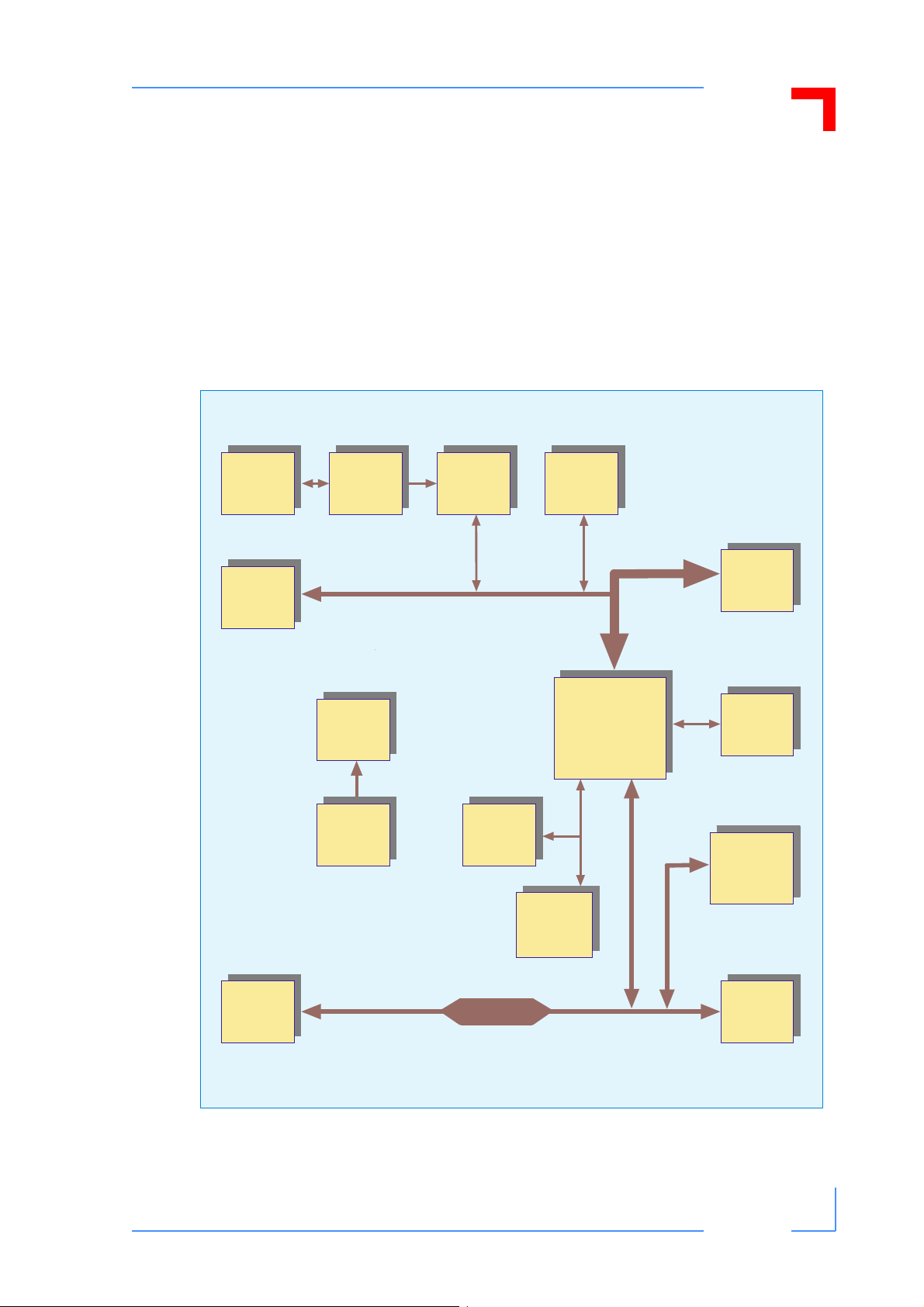
Figure 2-1: Functional Block Diagram
PUSH
BUTTONS/
LED’S
SERIAL
INTERFACE
2 × 16550
compatible
SYSTEM
LOGIC
Serial IRQ
(Registry
Watchdog)
POWER
SUPPLY
2 × DC/DC
RESET
GENERATION
FLASH
2 × 4MB
Port X (8 bit wide)
RTC
M41T56
FLASH
SOCKET
DIP600,
<52kB
CPU
Motorola
MPC 8240
200-250 MHz
Memory Bus
64-bit
SYSTEM
MEMORY
SDRAM
32 - 128 MB
DEBUG
JTAG/T est
interface
PCI
EXPANSION
CONNECTOR
EEPROM
I2C
FAST
ETHERNET
82559ER
PCI Bus
32-bit 33 MHz
ID 26037, Rev. 01 Page 2 - 3® 2002 PEP Modular Computers GmbH
VME
INTERFACE
Tundra
Universe II
Page 26
VMP1 Functional Description
2.2 Front Panels
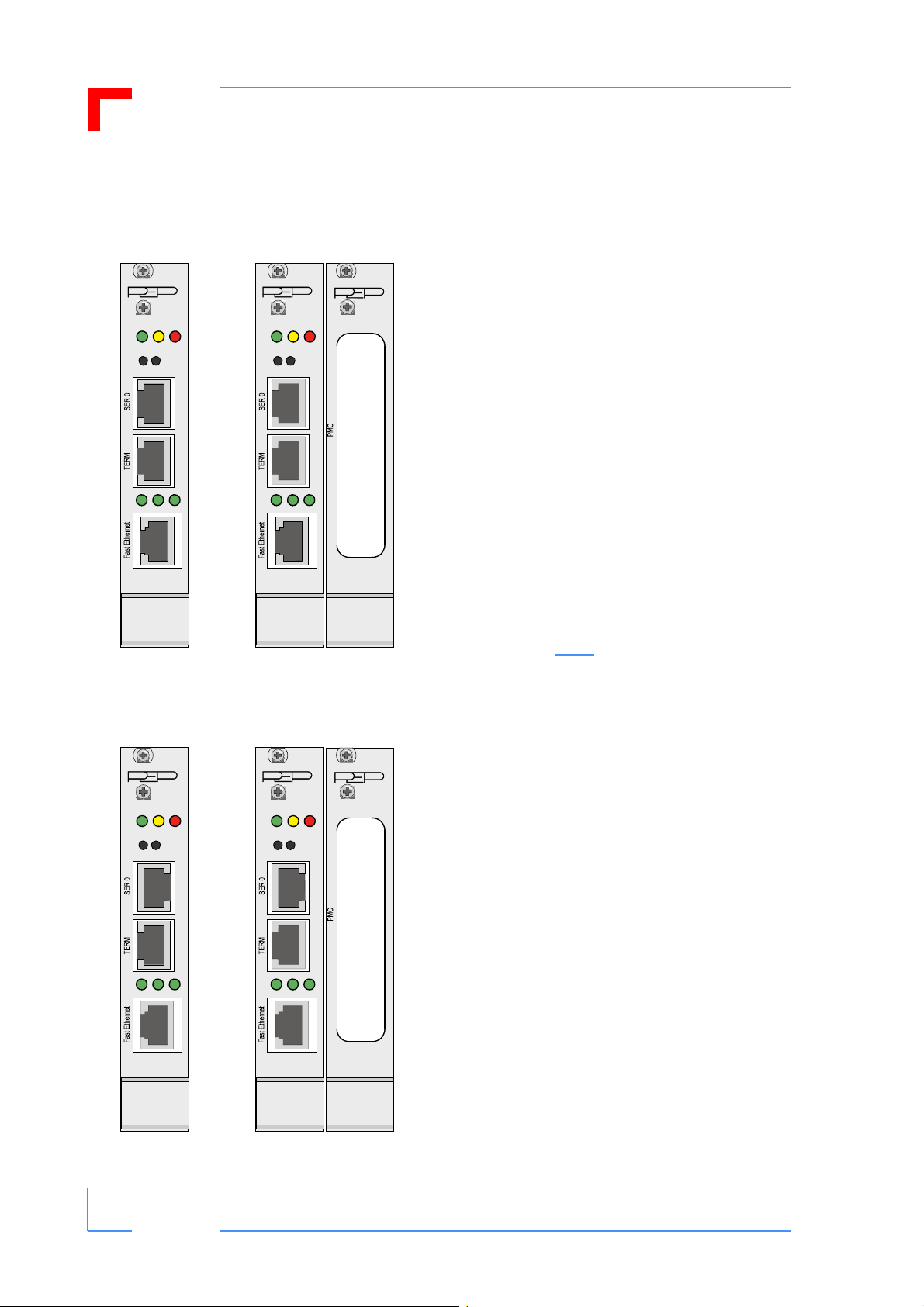
Figure 2-2: Front Panels
WUH WUH
ABRST
LNK.
SPEEDACT.
WUH
ABRST
LNK.
SPEEDACT.
VMP1VMP1
UH
W
VMP1-IO1
Standard VMP1 and
Standard with IO1 Module
KEY
LED colors
(for B&W monitors
and printouts):
U = green
W = yellow
H = red
ABRST
LNK.
VMP1
ABRST
VMP1 Optoisolated version
and Optoisolated version
with IO1 Module - note the
LNK.
SPEEDACT.
VMP1
SPEEDACT.
VMP1-IO1
different position of the
SER 0 connector
ID 26037, Rev. 01Page 2 - 4 ® 2002 PEP Modular Computers GmbH
Page 27
VMP1 Functional Description
2.3 Board Layout
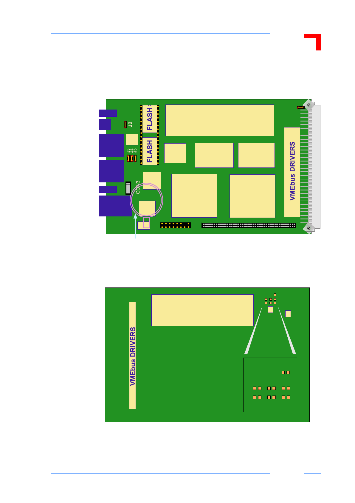
Figure 2-3: VMP1 Board (Front View)
1
LED
RJ45
GND
RTC
UART
X BUS
BUFFERS
ABORT
& RESET
(Serial)
RJ45
(Term.)
LOGIC
12
11
LED
ETHERNET
1
2
GOLDCAP
BATTERY
(Optional)
ETHERNET
CPU
216
CON10
115
JTAG
Figure 2-4: VMP1 Board (Reverse View)
SDRAM MEMORY
BANK 1
DC/DC DC/DC
PCI TO VME
BRIDGE
1
2
PCI EXPANSION CONNECTOR
CON11
J1
99
100
SDRAM MEMORY
BANK 2
R3
R8 R6R7
R11R12R13
MAGNIFIED
R3
R8 R6R7
R11R12R13
ID 26037, Rev. 01 Page 2 - 5® 2002 PEP Modular Computers GmbH
Page 28

VMP1 Functional Description
2.4 Main Features
The following descriptions provide an overview of the main features of the principa l functional blocks of the VMP1.
2.4.1 CPU
The VMP1 is based on the Motorola PowerPC processor MPC8240 which integrates a
large number of peripherals, such as a PCI interface, PCI arbiter, Interrupt Controller,
Memory Controller and multiple Timers. CPU speed is 250 MHz.
2.4.1.1 MPC8240 (Kahlua) Features
Important features of the MPC8240 implemented on the VMP1 are as follows:
Peripheral logic
Memory interface
• Programmable timing supporting either FPM DRAM, EDO DRAM or SDRAM
(The VMP1 uses SDRAM at 100 MHz)
• High bandwidth bus (64-bit data bus) to SDRAM
• 2 memory banks with up to 64 MB each (64 or 128 Mbit memory devices)
• Supports 32, 64, 96 and 128 MB SDRAM
• Contiguous memory mapping
• 8-bit ROM interface
• Write buffering for PCI and processor accesses
• Supports ECC
• SDRAM data path buffer
• Low voltage transistor-to-transistor logic (LVTTL)
• Port X: 8-bit general-purpose I/O port using ROM controller
interface with address strobe
32-bit PCI interface operating up to 33 MHz on the VMP1
• PCI Specification Revision 2.1 compatible
• PCI 5.0-V tolerance
• Support for PCI-locked accesses to memory
• Support for accesses to all PCI address spaces
• Selectable big- or little-endian operation
• Store gathering of processor-to-PCI write and PCI-to-memory write accesses
• Memory prefetching of PCI read accesses
• Selectable hardware-enforced coherency
• PCI bus arbitration unit (five request/grant pairs)
ID 26037, Rev. 01Page 2 - 6 ® 2002 PEP Modular Computers GmbH
Page 29

VMP1 Functional Description
PCI agent mode capability
• Address translation unit
• Internal configuration registers accessible from PCI
• Two-channel integrated DMA controller
• Supports direct mode or chaining mode (automatic linking of DMA transfers)
• Supports scatter gathering - read or write discontinuous memory
• Interrupt on completed segment, chain, and error
• Local-to-local memory
• PCI-to-PCI memory
• PCI-to-local memory
• Local-to-PCI memory
Message unit
• I2O message controller
• Two door-bell registers
• In-bound and out-bound messaging registers
I2C controller with full master/slave support
Embedded programmable interrupt controller (EPIC)
• Five hardware interrupts (IRQs) or 16 serial interrupts
• Four programmable timers
Integrated PCI bus and SDRAM clock generation
Programmable memory and PCI bus output drivers
Debug features
• Watchpoint monitor
• Address attribute and PCI attribute signals
• JTAG/COP - common onboard processor for in-circuit hardware debugging
• Performance monitor
603e core
High performance, superscalar 603e core
SPECint95 = 6.2 / SPECfp95 = 5.2 / 352Dhrystone (2.1) MIPS
Integer unit (IU), floating point unit (FPU) (user enabled or disabled), load/store unit
(LSU), system register unit (SRU), and a branch processing unit (BPU)
16 kB instruction cache
16 kB data cache
Lockable L1 cache - entire cache or on a per-way basis
Dynamic power management
ID 26037, Rev. 01 Page 2 - 7® 2002 PEP Modular Computers GmbH
Page 30

VMP1 Functional Description
2.4.2 Memory
2.4.2.1 System Memory (DRAM)
The main memory of the VMP1 consists of 32 MB or 64 MB SDRAM (128 MB available
on request) soldered onto the board for mechanical stability.
The VMP1 provides ECC support (optional) and a maximum memory speed of 100MHz.
2.4.2.2 Flash
4 or 8 MB of soldered Flash memory accommodate the bootstrap loader software and
can be used to store ROMable operating systems or user data. This Flash memory is 8bit wide and windowed with window sizes of 512 kB.
2.4.2.3 EEPROM
A serial EEPROM is provided, organised into 8 blocks with 256 bytes per block
(24LC16). This EEPROM is connected to the I2C bus provided by the MPC8240.
2.4.2.4 Memory Expansion Socket (DIL600)
The VMP1 provides one 32-pin DIL socket on which to place SRAM, non-volatile SRAM
or other DIL600 devices on the board. Access to this Memory is controlled by the
onboard logic.
The following devices may be added to the VMP1 via the 32-pin DIL600 socket:
• Standard Flash memory of up to 512 kB, for example, the AMD29F010 and
AMD29F040
• The NV SRAM from Dallas Semiconductor. These devices are available in the
temperature range –40°C to +85°C for the industrial environment and guarantee
a minimum data retention of 10 years (e.g. DS1250Y-100).
• Disk-on-chip Flash memory. In order to achieve flexibility with low cost, the VMP1
Flash disk is not soldered but connected via a special module from M-Systems
(Disk-on-Chip 2000) which comes in the following sizes:
2 - 24 MB (dimensions 41.7 x 17.9 x 5.6mm);
4 - 144 MB (dimensions 42.0 x 18.3 x 11.8mm).
ID 26037, Rev. 01Page 2 - 8 ® 2002 PEP Modular Computers GmbH
Page 31

VMP1 Functional Description
2.4.3 Board Interfaces
2.4.3.1 VME Interface and Pinout
The VME interface is based on the TUNDRA UNIVERSE II Bridge,
which includes the following features required for 3U VME systems:
• A24/A16 addressing modes capability
• D16/D8 data transfer capability
• Automatic First-Slot-Detection
• Single level BR3 arbitration release-when-done option
• FAIR VMEbus arbitration option
• ACFAIL NMI option
• SYSFAIL IRQ option
• System controller functions (SYSCLK, Bus monitor, Power monitor)
• Compatibility with PEP 3U VME system addressing schemes
• Compatibility with PEP VME backplane design and feature set
• Compatibility with PEP backplane transceiver logic
A table showing the pinout of the VME bus connector
appears on the following page.
PINROWS
ABC
1
32
ID 26037, Rev. 01 Page 2 - 9® 2002 PEP Modular Computers GmbH
Page 32

VMP1 Functional Description
VME Bus Connector Pinout
Table 2-1: Pin Assignment J1/P1 VME
Pin Number Pinrow A Pinrow B Pinrow C
1 D00 BBSY D08
2 D01 BCLR D09
3 D02 ACFAIL D10
4 D03 BG0IN D11
5 D04 BG0OUT D12
6 D05 BG1IN D13
7 D06 BG1OUT D14
8 D07 BG2IN D15
9 GND BG2OUT GND
10 SYSCLK BG3IN SYSFAIL
11 GND BG3OUT BERR
12 DS1 BR0 SYSRESET
13 DS0 BR1 LWORD
14 WRITE BR2 AM5
15 GND BR3 A23
16 DTACK AM0 A22
17 GND AM1 A21
18 AS AM2 A20
19 GND AM3 A19
20 IACK GND A18
21 IACKIN SERA A17
22 IACKOUT SERB A16
23 AM4 GND A15
24 A07 IRQ7 A14
25 A06 IRQ6 A13
26 A05 IRQ5 A12
27 A04 IRQ4 A11
28 A03 IRQ3 A10
29 A02 IRQ2 A09
30 A01 IRQ1 A08
31 -12V +5VSTDBY +12V
32 +5V +5V +5V
ID 26037, Rev. 01Page 2 - 10 ® 2002 PEP Modular Computers GmbH
Page 33

VMP1 Functional Description
2.4.3.2 Ethernet Connector and Pinout
The Ethernet interface is based on a PCI device
from Intel; the Ethernet Controller 82559ERS.
The main features of the Ethernet are as follows:
• integrated IEEE 802.3 10Base T and 100Base TX compatible PHY
• glueless 32-bit PCI master interface
• compatible with driver software of the 82558 and 82557
• full duplex support at both 10 and 100 Mbps
• IEEE 802.3u Auto-Negotiation support
• 4 kB transmit and 3 kB receive FIFO’s
Ethernet Connector Pinout
The connector used for the 100BaseTX Ethernet interface is an RJ45 connector.
The signals on this connector are as follows
Table 2-2: Ethernet RJ45 Pin Assignment
Pin Number Signal
1
8
1TX+
2TX3RX+
4nc
5nc
6RX7nc
8nc
ID 26037, Rev. 01 Page 2 - 11® 2002 PEP Modular Computers GmbH
Page 34

VMP1 Functional Description
2.4.3.3 Serial Interfaces and Pinouts
1
Two serial ports (RS232) are provided by means of two 8-pin
RJ45 connectors.
The RS232 serial interfaces named TERM and SER are 16C550 compliant and have
128-byte transmit and receive buffers. In addition to their other uses, the TERM port is
used to interface with the bootstrap loader and the SER port is used to download software.
Electrically, the two serial ports are identical and they provide a complete set of handshaking and modem control signals, maskable interrupt generation and data transfer of
up to 115.2 KBaud.
The upper serial interface (SER) can also be configured to act as an RS485 interface.
The configuration of the interface is achieved by setting the RS_CTL bit in the Control
Register. Please refer to Table 4-14 in chapter 4.
Additionally, a module is available from PEP which provides an optoisolated half/full
duplex RS485 interface. For this reason the onboard SER connector on the VMP1
baseboard is not equipped. Please contact PEP Support department for more information.
Pinouts of Serial Ports (RJ45 Connectors)
8
Table 2-3: Serial Port Pin Assignment
RS485
Pin Number Signal
Signal Half-duplex Signal Full-duplex
1DSRNC-RxD
2 RTS NC NC
3 GND GND GND
4TXD+TRXD-TxD
5 RXD NC NC
6DCDNC+RxD
7CTS-TRXD+TxD
8 DTR NC NC
ID 26037, Rev. 01Page 2 - 12 ® 2002 PEP Modular Computers GmbH
Page 35

VMP1 Functional Description
2.4.3.4 PCI Expansion Connector and Pinout
Figure 2-5: PCI Expansion Connector
1
PCI EXPANSION CONNECTORCON11
2
The PCI Expansion Connector provides the possibility to mount several transition
boards above the VMP1 for adding special functionality which is not provided on the
VMP1 main board or on the VME bus. All the PCI signals of the on board PCI bu s will be
routed to this connector, so that a complete PCI bus is provided on this connector. In
addition, almost the same number of ground and power pins (3.3V and 5V) as are on a
CPCI P1 or PMC connector are provided. Examples of transition boards are:
• PMC carrier
• PC-MIP carrier
• IO board with Graphic interface, second Ethernet interface, SCSI etc.
99
100
A table showing the pinout of the PCI Expansion Connector
appears on the following page.
ID 26037, Rev. 01 Page 2 - 13® 2002 PEP Modular Computers GmbH
Page 36

VMP1 Functional Description
PCI Expansion Connector (CON11) Pinout
Table 2-4: PCI Expansion Connector Pinout
Signal Pin Number Pin Number Signal
GND
1)
RST# 3 4
+3.3V
2)
CLK3 7 8
GND
1)
12SCL (I2C)
+3.3V
2)
56CLK2
GND
1)
910CLK4
INTB# 11 12 INTA#
INTD#1314INTC#
+5V
3)
GNT#3 17 18
+3.3V
2)
GND
1)
REQ#3 23 24
+5V
3)
15 16 GNT#2
+5V
3)
19 20 GNT#4
21 22 REQ#2
GND
25 26 REQ#4
1)
AD31 27 28 AD30
AD29 29 30
GND
1)
31 32 AD28
+5V
3)
AD27 33 34 AD26
AD25 35 36
+3.3V
2)
37 38 AD24
GND
1)
C/BE3# 39 40 SDA (I2C)
AD23 41 42
GND
1)
43 44 AD22
+3.3V
2)
AD21 45 46 AD20
AD19 47 48
+5V
3)
49 50 AD18
GND
1)
AD17 51 52 AD16
C/BE2# 53 54
GND
1)
55 56 FRAME#
IRDY# 57 58
+3.3V
2)
59 60 TRDY#
DEVSEL# 61 62
GND
1)
63 64 STOP#
LOCK# 65 66
+5V
3)
GND
GND
+3.3V
1)
1)
2)
Table continued on following page
ID 26037, Rev. 01Page 2 - 14 ® 2002 PEP Modular Computers GmbH
Page 37

VMP1 Functional Description
Table 2-4: PCI Expansion Connector Pinout
Signal Pin Number Pin Number Signal
PERR# 67 68
SERR# 69 70
+5V
3)
71 72 PAR
+5V
GND
3)
1)
C/BE1# 73 74 AD15
AD14 75 76
GND
1)
77 78 AD13
+3.3V
2)
AD127980AD11
AD10 81 82
GND
1)
83 84 AD9
GND
1)
AD8 85 86 C/BE0#
AD7 87 88
+3.3V
2)
89 90 AD6
+5V
3)
AD5 91 92 AD4
AD3 93 94
GND
1)
95 96 AD2
GND
1)
AD1 97 98 AD0
+12V
4)
99 100
-12V
5)
1) Ground
2) +3.3V
3) +5V
Key
4) +12V
5) -12V
ID 26037, Rev. 01 Page 2 - 15® 2002 PEP Modular Computers GmbH
Page 38

VMP1 Functional Description
2.4.3.5 Serial Interface Expansion Connector and Pinout
The serial interface expansion connector provides the capability to add different front
end interfaces to the UART B signals. For example, an opto-isolated RS422/485 module
(currently under development) may be plugged onto this connector.
Serial Interface Expansion Connector CON3 Pinout
Table 3-5: Serial Interface Expansion Connector (CON3) Pinout
Pin Number Function Function Pin Number
1GNDRTSB2
3REDE4
5RxDTxD6
7CTSDTR8
9SCLSDA10
11 +3.3V VCC 12
2.4.3.6 Memory Expansion Connector
A 32-pin DIL600 socket is provided in order to make possible the addition
of various memory expansion devices (with access time <120ns). The
devices which have been tested and approved for this connector are as follows:-
DIL type Flash memory (up to 512 kB)
DIL SRAM (up to 512 kB) e.g. Samsung KM684000BLP-7
NVSRAM (up to 512 kB) e.g. DALLAS DS1250Y-100)
Eprom (up to 512 kB) e.g. 27C040
M-Systems DiskOnChip 2000 (up to 288 MB)
Note:
For the pinout of this connector please see Chapter 4,
section 4.2.1
1
ID 26037, Rev. 01Page 2 - 16 ® 2002 PEP Modular Computers GmbH
Page 39

VMP1 Functional Description
2.4.3.7 DEBUG Interface and Pinout
216
CON10
A JTAG/BDM interface is provided on the VMP1 for software
debugging. The pinout of this connector is in accordance
with the pinout of the most commonly used emulator probes.
Note:
Debug Connector Pinout
Table 2-6: Debug Interface Connector (CON10) Pinout
TDO 1 2 NC
TDI 3 4 TRST#
NC 5 6 3.3V
TCK 7 8 NC
TMS 9 10 NC
SRESET# 11 12 NC
HRESET# 13 14 KEY (no pin)
CHKSTP#1516GND
As shipped, only the Altera onboard logic may be detected by
means of the JTAG interface. If the JTAG interface requires to be
re-configured for software debugging, please contact Support at
PEP Modular Computers for assistance.
Signal Pin Number Pin Number Signal
115
JT A G
2.4.4 Digital Temperature Sensor (LM75)
The VMP1 also provides an onboard digital temperature sensor with a thermal watchdog functionality (National Semiconductor LM75). This has various uses including, for
example, calibration of the onboard RTC over a wider temperature range.
ID 26037, Rev. 01 Page 2 - 17® 2002 PEP Modular Computers GmbH
Page 40

VMP1 Functional Description
2.5 Special Board Features
2.5.1 Watchdog Timer
A watchdog timer is provided, which forces an NMI or Reset condition (configurable in
the watchdog register). The watchdog time can be programmed in 4 steps with a resolution of 500 ms. If the watchdog timer is enabled, it cannot b e stopped or reprogrammed.
Table 2-7: Watchdog Time Values
Watchdog Time Values
500 ms
1 s
1.5s
2 s
2.5.2 RTC (STC M41T56)
The Real Time Clock provides the following features:
• counters for seconds, minutes, hours, day, date, month and year.
• clock calibration by software
• low supply current for buffering with Gold Caps
• alternatively a battery may be placed on the board to buffer the RTC for a longer
time
• it is also possible to buffer the power supply for the RTC via the VME-5V-Standby
power line
• automatic leap year compensation
• precision: 35 ppm
• for greater precision or for temperature compensation the RTC can be adjusted in
in steps of +4.068 or –2.034 ppm
• for temperature compensation, the onboard temperature sensor (LM75) may be
used
2.5.3 Reset/Abort
There are also 2 push button switches with the function ABORT and RESET. The
RESET button reinitializes the board via hardware.
The ABORT button initiates the NMI. In addition it is latched into a bit in the System
Logic, the purpose of this is to differentiate between the NMI initiated from the ABORT
Button and the NMI initiated from the watchdog.
buttons on the Front Panel may be viewed in Figure 2-2.
The positions of the Abort and Reset
ID 26037, Rev. 01Page 2 - 18 ® 2002 PEP Modular Computers GmbH
Page 41

VMP1 Functional Description
2.5.4 Front Panel LED’s
Three LED’s with the colors red, green and yellow are provided on the front panel
(please see Figure 2-2 on page 2-4) to give a quick indication of several key operating
conditions:
• The red LED (H) is general purpose.
• The yellow LED (W) indicates WATCHDOG ACTIVE
• The green LED (U) has been preset to light on initialisation of the board. After-
wards it is available for general purposes
The general purpose LED’s are programmable via a register in the System Logic.
3 additional LED’s, all green, are provided to indicate Ethernet working conditions:
• Ethernet Link Integrity
• Ethernet Activity
• Ethernet Speed
ID 26037, Rev. 01 Page 2 - 19® 2002 PEP Modular Computers GmbH
Page 42

This page was intentionally left blank.
® 2002 PEP Modular Computers GmbH
Page 43

VMP1
Installation
Installation
3.1 Board Installation ................................................................. 3 - 3
3.1.1 Front Panel I/O Connectors ........................................3 - 4
Chapter
3
ID 26037, Rev. 01
Page 3 - 1® 2002 PEP Modular Computers GmbH
Page 44

This page was intentionally left blank.
® 2002 PEP Modular Computers GmbH
Page 45

VMP1 Installation
3. Installation
The VMP1 has been designed for easy installation. However, the following importantstandard precautions must be observed. Some other important information is also set
out below.
3.1 Board Installation
Slot Selection
The VMP1 is designed so that it may be used in any free slot of a 3U VME Backplane.
It has an automatic first slot detection mechanism which configures it as a System Controller when placed in the far left slot.
When configured as the System Controller, it enables its system clock and arbiter in
order to control the entire VME bus.
Default setting of the serial Interfaces: 9600 Baud, 8N1
On initial startup a message of greeting comes up.
When the VMP1 is invoked for the first time, a Bootstrap loader startup messag e comes
up on the “term” serial port, which will provide you with some configuration information
on the system and a command prompt for entering bootstrap loader commands. For a
detailed description of these commands please see chapter 5 Bootstrap loader.
Caution!
Please switch off the VME system before installing the board in a
free slot. Failure to do so could endanger your life/health and may
damage your board or system.
Note:
Certain VME boards require bus master capability. If you are in
doubt whether such features are required for the board you intend
to install, please check your specific board and/or system documentation to make sure your system is provided with an appropriate free slot to insert the board.
ID 26037, Rev. 01 Page 3 - 3® 2002 PEP Modular Computers GmbH
Page 46

VMP1 Installation
ESD Equipment!
Your VMP1 board contains electrostatically sensitive devices.
Please observe the necessary precautions to avoid damage to
your board:
• Discharge your clothing before touching the assembly. Tools
must be discharged before use.
• Do not touch components, connector-pins or traces.
• If working at an anti-static workbench with professional discharging equipment, please do not omit to use it.
PEP Advantage
The VMP1 is designed to be bootstrapped from the Flash device
alone.
3.1.1 Front Panel I/O Connectors
Attention!
!
Due care should be exercised when connecting cabling in order to
avoid damage to your connected device and/or the VMP1 board.
For pinouts of the Front Panel connectors, please see Chapter 2:
Functional Description, sections 2.4.3.2 and 2.4.3.3
ID 26037, Rev. 01Page 3 - 4 ® 2002 PEP Modular Computers GmbH
Page 47

VMP1
Configuration
Configuration
4.1 Jumper Settings ..................................................................4 - 3
4.1.1 Bootstrap Loader / Socket Jumper J1 ......................... 4 - 3
4.1.2 RTC (Real-time clock) Calibration OutputJ2 ...............4 - 3
4.1.3 Resistor Setting for Non-standard Socket Devices ..... 4 - 4
4.1.4 RS485 Termination (Onboard Interface Only) ............ 4 - 4
4.2 Pinouts ................................................................................4 - 5
4.2.1 Flash Socket Type Selection ...................................... 4 - 5
Chapter
4
4.2.1.1 Socket Device Selection .......................................4 - 5
4.2.2 Serial Interface Expansion Connector (CON3) ........... 4 - 6
4.3 Board Address Map .............................................................4 - 7
4.3.1 Address Map Overview ............................................... 4 - 7
4.3.2 VME Address Area ..................................................... 4 - 8
4.3.3 Onboard Device Addresses ........................................ 4 - 9
4.3.4 Special Registers Overview ...................................... 4 - 10
4.3.4.1 Board Control Registers ......................................4 - 10
4.3.4.2 Board ID Register ............................................... 4 - 10
4.3.4.3 Software Compatibility ID .................................... 4 - 10
4.3.4.4 Memory Configuration Register .......................... 4 - 11
4.3.4.5 SDRAM Size .......................................................4 - 11
4.3.4.6 Flash Bank Select Register ................................. 4 - 11
4.3.4.7 Watchdog Control Register ................................. 4 - 12
4.3.4.8 Watchdog Timeout Time ..................................... 4 - 12
ID 26037, Rev. 01
Page 4 - 1® 2002 PEP Modular Computers GmbH
Page 48

VMP1
Configuration
Configuration
4.3.4.9 Control Register ..................................................4 - 13
4.3.4.10 Event Register .................................................... 4 - 13
4.3.4.11 Board / Logic Revision Register .........................4 - 14
4.3.4.12 UART A / Registers ............................................. 4 - 15
4.3.4.13 UART B / Registers ............................................. 4 - 16
4.3.5 IRQ Routing ..............................................................4 - 17
4.3.6 Real-time Clock .........................................................4 - 18
4.3.7 EEPROM .................................................................. 4 - 19
4.3.8 Digital Temperature Sensor ...................................... 4 - 19
ID 26037, Rev. 01
Page 4 - 2® 2002 PEP Modular Computers GmbH
Page 49

VMP1 Configuration
4. Configuration
4.1 Jumper Settings
Please see Figures 2-3 and 2-4 in Chapter 2 to view the positions of the jumpers and
resistors on the board.
4.1.1 Bootstrap Loader / Socket Jumper J1
The Jumper J1 is used to select the memory position from which the VMP1 fetches its
boot code. It determines the address position of the onboard Flash window and the
Flash/SRAM expansion socket (DIL600, 32-pin).
Table 4-1: Bootstrap Loader / Socket Jumper J1 Settings
J1 Meaning Address Assignment
VMP1 fetches
Open
Closed
Note: The MPC8240 initially fetches its boot code from address 0xFFF0 0100!
boot code from
onboard Flash
VMP1 fetches
boot code from
socket
Socket: 0xFFF8 0000 - 0xFFFF FFFF
Onboard Flash window: 0xFFF0 0000 - 0xFFF7 FFFF
Socket: 0xFFF0 0000 - 0xFFF7 FFFF
Onboard Flash window: 0xFFF8 0000 - 0xFFFF FFFF
4.1.2 RTC (Real-time clock) Calibration Output J2
Frequency test output is used for calibration of the onboard RTC. The RTC provides a
512 Hz frequency test signal for calibration purposes. Please refer to the datasheet of
the ST M41T56 for detailed information (for position of J2 on the board please see figure
2-3).
Warning!
!
J2 must not be bridged.
ID 26037, Rev. 01 Page 4 - 3® 2002 PEP Modular Computers GmbH
Page 50

VMP1 Configuration
4.1.3 Resistor Setting for Non-standard Socket Devices
The default pinout of this socket is designed for use with standard DIL Flashes and MSystems DiskOnChip. As some devices have a different pinout, resistors must be set
accordingly (please see figure 2-4 for an illustration of these resistors on the board)
Table 4-2: Resistor Setting for Various Non-standard Socket Devices
Used Socket Devices R3 R6 R7 R8 R11 R12 R13
Flash (default) Open Open Open Set Set Open Set
DiskOnChip (default) Open Open Open Set Set Open Set
NVSRAM Open Open Set Open Set Set Open
4 Mbit EPROM Set Set Open Open Open Open Set
Note: All resistors are 0 ohms
4.1.4 RS485 Termination (Onboard Interface Only)
When the VMP1 is using the onboard RS485 interface and is the last on the RS485 bus,
then the RS485 interface must provide termination resistance. The purpose of J3 is to
enable this line termination resistor (130 R).
Table 4-3: Jumper Settings for RS485 Termination
Termination J3
ON Set
OFF Open
Additionally, the correct idle line potential must be provided at one location within the
RS485 bus. J4 and J5 are used for this purpose. Pullup/Pulldown resistors are 380 Ohm
each.
Note:
Ensure that the reference potential for the RS485 signals are set
in one location only on the bus.
ID 26037, Rev. 01Page 4 - 4 ® 2002 PEP Modular Computers GmbH
Page 51

VMP1 Configuration
4.2 Pinouts
4.2.1 Flash Socket Type Selection
4.2.1.1 Socket Device Selection (Memory Expansion Socket IC8)
A range of different memory devices may be used on the DIL32 socket (e.g. Flashes,
NVSRAM, M-Systems Disk-On-Chip, EPROM etc.).
Table 4-4: DIL 32 Pinout for Various Devices
Pin
4Mbit
Flash
1 A18 NC A18 VPP VCC VCC VCC VCC 32
2
3
4
5
6
7
8
9
10
11
12
13
A16 NC A16 A16 A18 A15 WE_ WE 31
A15 NC A14 A15 A17 A17 NC A17 30
A12 A12 A12 A12 A14 WE NC A14 29
A7 A7 A7 A7 A13 A13 NC A13 28
A6 A6 A6 A6 A8 A8 A8 A8 27
A5 A5 A5 A5 A9 A9 A9 A9 26
A4 A4 A4 A4 A11 A11 A11 A11 25
A3 A3 A3 A3 OE_ OE_ OE_ OE_ 24
A2 A2 A2 A2 A10 A10 A10 A10 23
A1 A1 A1 A1 CE_ CE_ CE_ CE_ 22
A0 A0 A0 A0 D7 D7 D7 D7 21
D0 D0 D0 D0 D6 D6 D6 D6 20
Disk
OnChipNVSRAM
4Mbit
Eprom
4Mbit
EpromNVSRAM
Disk
OnChip
4Mbit
Flash
Pin
14
15
16
ID 26037, Rev. 01 Page 4 - 5® 2002 PEP Modular Computers GmbH
D1 D1 D1 D1 D5 D5 D5 D5 19
D2 D2 D2 D2 D4 D4 D4 D4 18
GND GND GND GND D3 D3 D3 D3 17
Page 52

VMP1 Configuration
4.2.2 Serial Interface Expansion Connector (CON3)
Table 4-5: RS Expansion Connector Pinout
Pin Number Function Function Pin Number
1GNDRTSB2
3REDE4
5RxDTxD6
7CTSDTR8
9SCLSDA10
11 +3.3V VCC 12
ID 26037, Rev. 01Page 4 - 6 ® 2002 PEP Modular Computers GmbH
Page 53

VMP1 Configuration
4.3 Board Address Map
4.3.1 Address Map Overview
Figure 4-1: VMP1 Address Map, 2 MB 8-bit Bank
0xFFFF FFFF
0xFEC0 0000
Reset Entry
0xFFF0 0100
BANK0
mirror Bank 0
0xFFE0 0000
0xFFE0 0000
0x8000 0000
0x4000 0000
0x0000 0000
PCI / VME
RESERVED
DRAM
unusable
PCI Interrupt Ack
Configuration DATA
+
Configuration
Address
0xFF80 0000
0xFF00 0000
0xFEF0 0000
0xFEE0 0000
0xFEC0 0000
ID 26037, Rev. 01 Page 4 - 7® 2002 PEP Modular Computers GmbH
Page 54

VMP1 Configuration
4.3.2 VME Address Area
Figure 4-2: VME Address Area
0x8FFF FFFF
currently unused
0x8800 0000
VME A24/D16
0x8700 0000
currently unused
0x8501 0000
VME A16/D16
0x8500 0000
currently unused
0x8400 0000
VME USER2
0x8300 0000
VME USER1
0x8200 0000
currently unused
0x8000 0000
VME bus slave address and VME IRQ mask are programmable inside the TUNDRA
UNIVERSE II. Please refer to the VME slave manual chapter in the TUNDRA UNIVERSE II manual and the BSP documentation.
ID 26037, Rev. 01Page 4 - 8 ® 2002 PEP Modular Computers GmbH
Page 55

VMP1 Configuration
4.3.3 Onboard Device Addresses
Figure 4-3: VMP1 Device Address Map
Reset Entry
0xFFFF 0100
Note:
soldered FLASH,
(512k page)
0xFFF8 0000
Socket
0xFFF0 0000
reserved reserved
0xFFE8 0000
Onboard Register
+
UART B
UART A
Boot jumper J1 installed Boot jumper J1 removed
0xFFE0 0010
0xFFE0 0008
0xFFE0 0000
Socket
soldered FLASH,
(512k page)
Onboard Register
+
UART B
UART A
0xFFF8 0000
0xFFF0 0000
0xFFE8 0000
0xFFE0 0010
0xFFE0 0008
0xFFE0 0000
• For write access to this address area (0xFFE0 0000-0xFFFF
FFFF), it is only possible to use byte-wide write commands.
• When the memory expansion socket is used for NVSRAM, byte
0xFFF0 0000 (J1 installed) or byte 0xFFF8 0000 (J1 removed)
is reserved for the output of post codes to the VMP1-Post. Data
should not be stored at either of these locations.
ID 26037, Rev. 01 Page 4 - 9® 2002 PEP Modular Computers GmbH
Page 56

VMP1 Configuration
4.3.4 Special Registers Overview
The Special Registers may be attached through read and write operation to the address
space FFe8 0000-FFF0 0000
4.3.4.1 Board Control Registers
Table 4-6: Board Control Registers
Register Address Read/Write
Board-ID FFe0 0010 R
Software Compatibility ID FFe0 0012 R
Memory Configuration FFe0 0014 R
Flash Bank Select FFe0 0016 R/W
Watchdog Control Register FFe0 0018 R/W
Control Register FFe0 001a R/W
Event Register FFe0 001c R/W
Board/Logic Revision FFe0 001e R
4.3.4.2 Board ID Register
Table 4-7: Board ID Register
Register Address MSB 6 5 4 3 2 1 LSB
Board ID FFe0 0010 BID7 BID6 BID5 BID4 BID3 BID2 BID1 BID0
The Board ID can be used to identify the VMP1 in a VME system. The value for the
VMP1 is 00h.
• This register is READ ONLY
4.3.4.3 Software Compatibility ID
Table 4-8: Software Compatibility ID
Register Address MSB 6 5 4 3 2 1 LSB
Software Compatibility ID FFe0 0012 SC7 SC6 SC5 SC4 SC3 SC2 SC1 SC0
The Software Compatibility ID will signal to the software when differences in hardware
require different handling by the software. This register is READ ONLY. It starts with the
value 0x00 and will be incremented with each change in hardware (software sensitive
only).
ID 26037, Rev. 01Page 4 - 10 ® 2002 PEP Modular Computers GmbH
Page 57

VMP1 Configuration
4.3.4.4 Memory Configuration Register
Table 4-9: Memory Configuration Register
Register Address MSB 6 5 4 3 2 1 LSB
Me m ory C onfigu r ati o n F Fe0 0014 BJ Res. Res. ECC Res. Res. SZ1 SZ0
• Bits SZ0 and SZ1 are used to identify the soldered SDRAM size.
• Bit 2 and Bit 3 are reserved
• Bit 4 (ECC) is used to indicate that ECC is supported (1 = ECC enabled)
• Bit MSB (BJ) indicates the status of the BOOT JUMPER (jumper J1 for exchanging Socket and Flash Chip Select). 0 = boot jumper set, 1 = boot jumper removed
4.3.4.5 SDRAM Size
Table 4-10: SDRAM Size
SZ1 SZ0 Meaning
0 0 32 MB/ 1 Bank
0 1 64 MB/ 2 Banks
10Reserved
11Reserved
4.3.4.6 Flash Bank Select Register
Table 4-11: Flash Bank Select Register
Register Address MSB 6 5 4 3 2 1 LSB
Flash bank select FFe0 0016 Res. Res. Res. Res. FB3 FB2 FB1 FB0
The Flash bank select register is used to select the appropriate Flash bank. As 8-bit
wide Flash memory may only be accessed through a 512 kB window; this is the only
way to address a larger size Flash memory. Using bits FB0..FB3, 16 Flash banks can be
selected (16x512 kB = 8 MB). The default value on startup of the VMP1 is 0x00.
ID 26037, Rev. 01 Page 4 - 11® 2002 PEP Modular Computers GmbH
Page 58

VMP1 Configuration
4.3.4.7 Watchdog Control Register
Table 4-12: Watchdog Control Register
Register Address MSB 6 5 4 3 2 1 LSB
Watchdog
control
FFe 0 001 8 WD_EN WD_R Res. WD_TRG Res. Res. WDT1 WDT0
4.3.4.8 Watchdog Timeout Time
Bits WDT0 and WDT1 are programmed to select the Watchdog timeout value.
Table 4-13: Watchdog Timeout Time
WDT1 WDT0 Time
0 0 0,5s
011s
1 0 1,5s
112s
• Bits 2 and 3 are reserved
• Bit WD_TRG retriggers the watchdog timer. A “1” written to this bit sets the watchdog back to its start condition.
• Bit 5 is reserved
• Bit WD_R (Watchdog Route). If set to 0 (default), then the watchdog timer causes
a reset, If set to 1, the watchdog timer will generate the NMI
• Bit 7: WD_EN: A “1” written to this bit starts the Watchdog. Once it has been
enabled it cannot later be disabled.
ID 26037, Rev. 01Page 4 - 12 ® 2002 PEP Modular Computers GmbH
Page 59

VMP1 Configuration
4.3.4.9 Control Register
Table 4-14: Control Register
Register Address MSB 6 5 4 3 2 1 LSB
Control FFe0 001a RS_CTL Res. Res. S_RST Res. Res. LED2* LED1*
• Bits 0 – 1: A “1” written to these bits lights the LED’s (LED1* is the green LED of
the top set on the front panel and LED2* is the red one)
• Bits 2 – 3 are reserved
• Bit S_RST: A “1” written to this bit initiates a Software Reset
• Bits 5 – 6 are reserved
• Bit 7: A “0” written to this bit configures the onboard SER connector to act as an
RS232 interface. A “1” written to this bit configures the onboard SER connector to
act as an RS485 interface (not optoisolated/half duplex)(default = 0)
Warning:
!
4.3.4.10 Event Register
Table 4-15: Event Register
Register Address MSB 6 5 4 3 2 1 LSB
Event FFe0 001c NLRST Res. Res. Res. Res. PB2 Res. WD
• Bit WD is used to indicate that a watchdog overrun has occurred (logic 1 if
condition has occurred)
• Bit 1 is reserved
• Bit PB2 is used to indicate that the abort button has been pressed (logic 1 if this
condition has occurred)
• Bits 3 - 6 are reserved
• Bit 7: ”NOT LRST” – this bit shows the status of the LRST pin of the
TUNDRA UNIVERSE II (important for bootstrap loader).
When setting bit 7 the user must ensure that the corresponding
interface is also an RS485. A mismatch will risk damage to the
VMP1 and/or the application.
ID 26037, Rev. 01 Page 4 - 13® 2002 PEP Modular Computers GmbH
Page 60

VMP1 Configuration
4.3.4.11 Board / Logic Revision Register
Table 4-16: Board / Logic Revision Register
Register Address MSB 6 5 4 3 2 1 LSB
Boar d r ev i s io n FFE0 001e LR 3 LR2 LR 1 LR 0 BR 3 BR2 BR1 BR0
The Board Revision Register may be used to identify the hardware and logic status of
the board by the software. It starts with the value 0x00 for the initial board prototypes
and will be incremented with each redesign / logic release.
• This register is READ ONLY.
ID 26037, Rev. 01Page 4 - 14 ® 2002 PEP Modular Computers GmbH
Page 61

VMP1 Configuration
4.3.4.12 UART A / Registers
For a detailed description please refer to the EXAR XR16C 2850 DUART manual.
The UART A occupies the following addresses:
Table 4-17: General Register Set (THR/RHR, IER/ISR, MCR/MSR, LCR/LSR, SPR)
Read Mode Write Mode Address
Receive Holding Register
Interrupt Status Register
Line Status Register -- FFe0 0005
Modem Status Register -- FFe0 0006
Scratchpad Register Scratchpad Register FFe0 0007
Transmit Holding Register
Interrupt Enable Register
FIFO Control Register
Line Control Register (LCR)
Modem Control Register
FFe0 0000
FFe0 0001
FFe0 0002
FFe0 0003
FFe0 0004
Table 4-18: Baud Rate Register Set (DLL/DLM)
Read Mode Write Mode Address
LSB of divisor latch LSB of divisor latch FFe0 0000
MSB of divisor latch MSB of divisor latch FFe0 0001
Table 4-19: Enhanced Register Set
Read Mode Write Mode Address
Trigger Level Register Trigger Level Register FFe0 0000
Feature Control Register Feature Control Register FFe0 0001
Enhanced Feature Register Enhanced Feature Register FFe0 0002
Enhanced Mode Select Register
Xon-1 Xon-1 FFe0 0004
Xon-2 Xon-2 FFe0 0005
Xoff-1 Xoff-1 FFe0 0006
Xoff-2 Xoff-2 FFe0 0007
ID 26037, Rev. 01 Page 4 - 15® 2002 PEP Modular Computers GmbH
Enhanced Mode Select
Register
FFe0 0007
Page 62

VMP1 Configuration
4.3.4.13 UART B / Registers
For a detailed description please refer to the EXAR XR16C 2850 DUART manual
The UART B occupies the following addresses:.
Table 4-20: General Register Set (THR/RHR, IER/ISR, MCR/MSR, LCR/LSR, SPR)
Read Mode Write M od e Address
Receive Holding register Transmit Holding Register FFe0 0008
-- Interrupt Enable Register FFe0 0009
Interrupt Status register FIFO Control Register FFe0 000a
-- Line Control Register FFe0 000b
-- Modem Control Register FFe0 000c
Line Status register -- FFe0 000d
Modem Status register -- FFe0 000e
Scratchpad register Scratchpad Register FFe0 000f
Table 4-21: Baud Rate Register Set (DLL/DLM)
Read Mode Write M od e Address
LSB of divisor latch LSB of divisor latch FFe0 0008
MSB of divisor latch MSB of divisor latch FFe0 0009
Table 4-22: Enhanced Register Set
Read Mode Write M od e Address
Trigger level register Trigger level register FFe0 0008
Feature Control register Feature control register FFe0 0009
Enhanced feature register Enhanced feature register FFe0 000a
Enhanced mode select register Enhanced mode select register FFe0 000f
Xon-1 Xon-1 FFe0 000c
Xon-2 Xon-2 FFe0 000d
Xoff-1 Xoff-1 FFe0 000e
Xoff-2 Xoff-2 FFe0 000f
ID 26037, Rev. 01Page 4 - 16 ® 2002 PEP Modular Computers GmbH
Page 63

VMP1 Configuration
4.3.5 IRQ Routing
Table 4-23: Serial IRQ’s
IRQ Name Source
S_IRQ0 Reserved
S_IRQ1 UART-A
S_IRQ2 UART-B
S_IRQ3 INTA# (PCI)
S_IRQ4 INTB# (PCI)
S_IRQ5 INTC# (PCI)
S_IRQ6 INTD# (PCI)
S_IRQ7 Temperature sensor interrupt
S_IRQ8 LINT0# / VME Interrupt level 1 and 2
S_IRQ9 LINT1# / unused
S_IRQ10 LINT2# / VME Interru pt level 3 and 4
S_IRQ11 LINT3# / VME Interru pt level 5 and 6
S_IRQ12 LINT4# / VME Interru pt level 7 + SYSFAIL
S_IRQ13 LINT5# / VME ACFAIL
S_IRQ14 LINT6# / 4 location monitors
S_IRQ15 LINT7# / 4 mailboxes
ID 26037, Rev. 01 Page 4 - 17® 2002 PEP Modular Computers GmbH
Page 64

VMP1 Configuration
4.3.6 Real-time Clock
Access to the RTC is effected via the I2C bus. The RTC uses address 0xD0
For more detailed information please refer to the manuals for the
ST - Microelectronics M41T56 and the Motorola MPC 8240 (I2C - Bus).
Table 4-24: Register Map RTC M41T56
Address D7 D6 D5 D4 D3 D2 D1 D0
0 ST 10 Seconds Seconds Seconds / 00-59
1 X 10 Minutes Minutes Minutes / 00-59
2 CEB CB 10 Hours Hour s
3 X X X X X Day Day / 00-07
4 X X 10 Date Date Date / 01-31
5XXX
6 10 Years Years Year / 00-99
7 OUT FT S Calibraton Control
Meanings of abbreviations in Table 4-24
CEB = Century enable bit
CB = Century bit
10
M.
Month Month / 01-12
Function/Range
in BCD Format
Century 0-1/Hour
00-23
FT = Frequency test bit
OUT = Output level
ST = Stop bit
S = Sign bit
Note:
When the RTC has once been stopped due to low voltage, it is
necessary to re-initialize the “Seconds” “Minutes” and “Hours” registers before it will run again.
ID 26037, Rev. 01Page 4 - 18 ® 2002 PEP Modular Computers GmbH
Page 65

VMP1 Configuration
4.3.7 EEPROM
Access to the EEPROM is effected via the I2C bus of the MPC8240. The EEPROM
uses the I2C address 0xA0.
For more detailed information please refer to the manuals for the MICROCHIP 24LC16B
and the MOTOROLA MPC8240 (I2C bus).
4.3.8 Digital Temperature Sensor
Access to the onboard temperature sensor is effected via the I2C bus of the MPC8240.
The EEPROM uses the I2C address 0x90.
For more detailed information please refer to the manuals for the National Semiconductor LM75 and the MOTOROLA MPC8240 (I2C bus).
ID 26037, Rev. 01 Page 4 - 19® 2002 PEP Modular Computers GmbH
Page 66

This page was intentionally left blank.
® 2002 PEP Modular Computers GmbH
Page 67

VMP1 NetBootLoader
Chapter
NetBootLoader
5.1 General Operation ...............................................................5 - 3
5.2 NetBootLoader Interfaces .................................................... 5 - 3
5.2.1 ABT (Abort) Switch .........................................................5 - 4
5.2.2 TERM Serial Interface ....................................................5 - 4
5.2.3 SER0 Serial Interface ..................................................... 5 - 4
5.2.4 Ethernet Interface ...........................................................5 - 4
5.3 NetBootLoader Functions .................................................... 5 - 4
5
5.3.1 NetBootLoader Control ................................................... 5 - 5
5.3.2 System Status Monitoring .............................................. 5 - 5
5.3.3 ftp Server Access ........................................................... 5 - 6
5.3.4 FLASH Operation ........................................................... 5 - 6
5.3.5 Motorola S-Records ....................................................... 5 - 6
5.4 Operating the NetBootLoader ............................................. 5 - 7
5.4.1 Initial Setup ..................................................................... 5 - 7
5.4.2 Accessing the NetBootLoader ........................................ 5 - 7
5.4.3 NetBootLoader Configuration ......................................... 5 - 8
5.4.4 telnet Login .....................................................................5 - 9
5.4.5 FLASH Operations ......................................................... 5 - 9
5.4.6 Updating the NetBootLoader ........................................ 5 - 11
5.4.7 Uploading a FLASH Area ............................................. 5 - 12
ID 26037, Rev. 01 © 2002 PEP Modular Computers GmbH Page 5 - 1
Page 68

NetBootLoader VMP1
5.5 Plug and Play .................................................................... 5 - 12
5.6 Porting an Operating System to the CPU Board ............... 5 - 12
5.7 Commands ........................................................................5 - 13
Page 5 - 2 © 2002 PEP Modular Computers GmbH ID 26037, Rev. 01
Page 69

VMP1 NetBootLoader
5. NetBootLoader
The CPU board is delivered with the NetBootLoader software already programmed into the onboard soldered Flash memory . The NetBootLoader it self is a software utility which initializes the
CPU board for operation before turning control over to either an application or to an operator.
This software also provides the capability to monitor and control the operation of the NetBootLoader itself, 01display system status information, to program execut able code and dat a to the
Flash memory, and to load and start application software.
To attain full operational capability, the NetBootLoader FLASH must be programmed by the
user with application software. Once the application has been programmed to Flash memory,
the NetBootLoader will support the complete boot operation. The following chapters describe
the functioning of the NetBootLoader and how to program the Flash memory.
5.1 General Operation
Upon power on or a system reset, the NetBootLoader is started. The CPU board is configured
for operation and control is either passed to an application or an operator. In the event a valid
application has been programmed into the Flash memory and no operator intervention takes
place, the application is copied from FLASH into SDRAM and control is p assed to the application. If the NetBootLoader does not find a valid application or operator intervention has occurred, control is passed to the operator . The operator now has control to determine the system
status, make configuration changes, read or program the Flash memory, or to restart or shut
down the system.
The operator command interfacing with the NetBootLoader is accomplished either via the
TERM serial port or the Ethernet port. During the boot operation a command interpreter is st arted which allows the operator to input commands to the NetBootLoader. Prior to interfacing via
the Ethernet port the network must be configured. This is done via the TERM port.
5.2 NetBootLoader Interfaces
There are four possibilities to interface with the NetBootLoader:
• Via the ABT (Abort) switch
• Via the TERM serial interface
• Via the SER0 serial interface
• Via the Ethernet interface
Gaining access to the NetBootLoader is a function of the contents of the Flash memory and the
“BootWaitT ime ” setting. If there is no valid application progra mmed into the Flash memory, the
boot operation automatically terminates after the CPU board has been initialized and control is
passed to the command interpreter. If there is a valid application in the Flash memory the boot
operation is delayed according to the setting of the boot wait time. The green user LED (U) on
the front panel flashes indicating that the boot operation is in a wait state. During this time the
operator may intervene in the boot operation either by pressing the ABT (Abort) switch, entering the “abort” command via the TERM interface, or by performing a su ccessful telnet login via
the Ethernet interface. If the operator does not intervene, the boot operation is continued after
the boot wait time has been exceeded.
ID 26037, Rev. 01 © 2002 PEP Modular Computers GmbH Page 5 - 3
Page 70

NetBootLoader VMP1
5.2.1 ABT (Abort) Switch
The ABT switch, located on the CPU board front panel, provides the operato r with the ability to
directly terminate the boot operation during the boot wait time which is indicated by the “U” LED
blinking. This is the sole purpose of the ABT switch during the NetBootLoader operation.
5.2.2 TERM Serial Interface
The TERM serial port is used to provide direct operator interfacing to the NetBootLoader. As
soon as the CPU board has been initialized this port is activated and the operator may input
commands. During the boot wait time the operator may terminate the boot operation and take
control of the NetBootLoader. Once the boot wait time is exceeded the command interpreter is
deactivated and the operator no longer has access to the NetBootLoader.
The TERM serial interface may either be directly connected to a terminal device or may interface with a terminal emulator.
5.2.3 SER0 Serial Interface
The SER0 serial port is used to provide the NetBootLoader with the ability to access Motorola
S-Records for programming an application to FLASH. No command interpreter is available for
this interface.
5.2.4 Ethernet Interface
The Ethernet interface provides the capability of remotely interfacing with the NetBootLoader.
Prior to using this interface it is necessary to configure the NetBootLoader network settings.
This is accomplished via the TERM interface. Once the network settings have been made, the
remote operator has the same capabilities as with the TERM interface. During the boot wait
time the operator gains control of the NetBootLoader by logging into it via the Ethernet interface. This causes the boot operation to be terminated and gives control to the remote operator.
The Ethernet interface uses the telnet protocol for operator interfacing with the NetBootLoader.
In addition to the operator interface via Ethernet, the NetBootLoader also uses the Ethernet interface for ftp server access.
5.3 NetBootLoader Functions
In addition to initializing the CPU board for operation and the loading and starting of applications, the NetBootLoader provides the following operator monitor and control functions:
• NetBootLoader control
• system status monitoring
• ftp server access
• FLASH reading and programming operations
• Motorola S-Record acquisition
These functions are described in detail in the following chapters.
NOTE ...
The command title (CMD TITLE) is expressed in capital letters and is not the
same as the syntax of the command. The command syntax is always written
using small letters
Page 5 - 4 © 2002 PEP Modular Computers GmbH ID 26037, Rev. 01
Page 71

VMP1 NetBootLoader
5.3.1 NetBootLoader Control
The NetBootLoader provides various functions for controlling the operation of the NetBootLoader itself as well as the setting of operational parameters. The following table provides an
overview of available NetBootLoader control functions.
Table 5-1: NetBootLoader Control Commands
CMD TITLE ALIAS FUNCTION REMARKS
ABORT - Terminate boot wait
BW Boot Wait Set or display BootWaitTime
HELP or ? - Display online HELP pages
LOGOUT - Terminate telnet session
NET - Set network parameters Must be set before attempting telnet login
PASSWD Password Set telnet password
PF Port Format Set serial port parameters Used for both TERM and SER0 ports
RS Reset Resets sy stem
5.3.2 System Status Monitoring
The NetBootLoader provides various functions for monitoring the overall status of the system
during the operation of the NetBootLoader. The following table provides an overview of available system status monitoring functions.
Table 5-2: System Status Monitoring Commands
CMD TITLE ALIAS FUNCTION REMARKS
CHECK - Application validation Verifies validity of user image programmed
to FLASH
INFO - Display system information
MD Memory
Display
Display memory contents Applies to all visible memory
PCI - Display PCI device information
PING - Verify network status
VER Version D isplay version number of
NetBootLoader
ID 26037, Rev. 01 © 2002 PEP Modular Computers GmbH Page 5 - 5
Page 72

NetBootLoader VMP1
5.3.3 ftp Server Access
The NetBootLoader provides various functions for interfacing with an ftp server. The following
table provides an overview of available ftp server functions.
Table 5-3: ftp Server Commands
CMD TITLE ALIAS FUNCTION REMARKS
BYE - Terminate session with ftp server
CD Change
Directory
GET - Download a file from ftp server Only for executable applications.
LOGIN - Login to ftp server
LS List Directory List ftp server di rectory Lists contents of directory.
PUT - Upload a file to ftp server Data buffer is source.
PWD Print Working
Directory
Change ftp server directory
Data buffer is target.
Display current ftp server directory Lists name of directory
5.3.4 FLASH Operation
The NetBootLoader provides various functions for performing operations with Flash memory.
The following table provides an overview of available FLASH operation functions.
Table 5-4: FLASH Operation Commands
CMD TITLE ALIAS FUNCTION REMARKS
CLONE - Program NetBootLoader to FLASH Uses data buffer or socket as source
LF Load FLASH Program application to FLASH Uses data buffer as source
SF Store FLASH Reads FLASH to data buffer Uses data buffer as target
5.3.5 Motorola S-Records
The NetBootLoader provides one function for acquiring Motorola S-Records. The follo wing table provides an overview of this function.
Table 5-5: Motorola S-Records Commands
CMD TITLE ALIAS FUNCTION REMARKS
SL SLoad Download Motorola S-Records Uses data buffer as target
Page 5 - 6 © 2002 PEP Modular Computers GmbH ID 26037, Rev. 01
Page 73

VMP1 NetBootLoader
5.4 Operating the NetBootLoader
5.4.1 Initial Setup
The CPU board is delivered with the NetBootLoader already installed in the onboard soldered
FLASH and is ready for operation. However , in order for the CPU board to be used in a system,
application software must be made available for use. This is accomplished by programming the
application also to the onboard soldered Flash memory where the NetBootLoader is located.
Upon initial power up the NetBootLoader is started automatically. As soon as the NetBootLoader has completed initialization of the CPU board, it checks to see if there is a valid application
programmed in FLASH and at the same time initiates a command interpreter which the operator can access either via the TERM or telnet interfaces. If there is no valid ap plication in memory, the NetBootLoader terminates the boot operation, and waits for operator intervention. As
this is the case when the CPU board is first powered up, the operator now ha s t he o pportun ity
to program an application.
Prior to programming an application it may be necessary to configure the NetBootLoader or
perform other functions depending on the user’s application development environment or application requirements. Once this has be accomplished and the application has been programmed, the CPU board is ready for operation.
The following chapters provide information on how to set up and operate the NetBootLoader
itself, initiation of the telnet interface, and how to program an application to FLASH.
5.4.2 Accessing the NetBootLoader
Initial access to the NetBootLoader can only be achieved via the TERM interface. Prior to using
the telnet interface, the Ethernet parameters must be set and this can only be accomplished
initially via the TERM interface. Once valid Ethernet parameters and the telnet log in password
have be set, the telnet interface is available for operation.
Use of the TERM interface requires either a terminal or a terminal emulator. Use of the telnet
interface requires a remote telnet login to the NetBootLoader.
Availability of the command interpreter depends on the system st atus. If there is no valid application programmed, the command interpreter is available as long as the operator requires it. If
a valid application is programmed, the command interpreter is only available for the duration of
the boot wait time. If the operator requires the command interpreter for a longer time he must
terminate the boot operation before the boot wait time is exceeded.
Upon initiation of the command interpreter, a prompt is sent to the TERM interface and commands may be entered. To gain access to the NetBootLoader from a remote location via Ethernet a telnet login must be performed. If the boot wait time has not been exceeded, a telnet login
automatically terminates the boot operation and a command prompt is sent to the telnet remote
interface.
Once the operator has control of the NetBootLoader, he may perform any required action. To
continue with the operation of the CPU board, the system must either be cold started or the
operator must issue a “reset” command. In either event, the NetBootLoader is restarted and
the boot operation begins anew.
ID 26037, Rev. 01 © 2002 PEP Modular Computers GmbH Page 5 - 7
Page 74

NetBootLoader VMP1
5.4.3 NetBootLoader Configuration
There are several NetBootLoader commands which provide the operator with the capability to
configure specific parameters which are used by the NetBootLoader for interfacing operations.
These commands are:
• BW (BootWait)
•NET
• PASSWD
• PF (Port Format)
Default settings are available for all the above commands except for “net” which is dependent
on the application environment.
5.4.3.1 BW
This command is used to display or set the actual boot wait time used by the NetBootLoader
to delay the boot operation before proceeding with the loading and starting of an application. If
this time is set too short it may only be possible to gain access to the NetBootLoader via the
“ABT” switch.
The BootWaitTime value is stored in the boot section of the serial EEPROM. This section is
validated with a CRC code to avoid the setting of random parameters.
Note ...
If the CRC of the boot section is not valid, changing the BootWaitTime will have
no effect because the “bw” command does not validate an invalid CRC. In this
case, a default timing of 5 seconds is always used.
To validate an invalid CRC, an operating system utility must be used, or, alternatively, the “-f”
option of the “bw” command must be issued.
Warning !!!
Using the “bw -f” command to validate invalid entries may adversely impact the
operation of the operating system.
5.4.3.2 NET
This command is used to set or display the parameters for the configuration of the Ethernet interface of the CPU board. The Ethernet interface is only available after these settings have
been made. Once these settings have been made, the system must be cold started or reset for
them to take effect.
5.4.3.3 PASSWD
This command is used to set the password used by the NetBo otLoader for the operation of the
telnet interface. No password is required for access from the TERM interface.
Page 5 - 8 © 2002 PEP Modular Computers GmbH ID 26037, Rev. 01
Page 75

VMP1 NetBootLoader
5.4.3.4 PF
This command is used to set the port parameters for the TERM a nd SER0 serial interfaces only
for the current operator session. The next system restart will cause these settings to revert to
the default settings of: 9600 Baud, 8 bits per character, 1 stop bit, and no parity. This is done
to preclude a system lockout when restarting due to incompatible settings.
5.4.4 telnet Login
A telnet login to the NetBootLoader is only possible during the boot wait time and only af ter the
Ethernet network parameters have been set.
T o ef fect a telnet login the operator performs the standard telnet log in procedure during the boot
wait time. The NetBootLoader responds by suspending the boot wait and requests a login
password. The operator then enters a password. If the password is valid, the boot wait is terminated and the operator can now access the NetBootLoader. If the password is invalid, the
telnet login procedure is terminated and the boot operation continues.
In the case of an invalid password, the login procedure may be repeated as often as required
within the boot wait time. Once the boot wait time is exceeded, a telnet login is no longer possible.
5.4.5 FLASH Operations
To achieve an operable system for an application, the application software must be programmed to FLASH. The NetBootLoader supports the programming of the application to
FLASH. In addition to this, it also supports the updating of the NetBootLoader itself as well as
data transfer from the FLASH to the data buffer and from the data buffer to an ftp server. The
following chapters provide information on performing the various types of FLASH operations.
5.4.5.1 FLASH Offsets
All FLASH is treated as one uniform FLASH, regardless of the physical addresses of the devices involved. If a DIL FLASH is plugged in the Memory Expansion socket, it is added to the
FLASH area as well. All offsets are based from the beginning of the FLASH area. This means
that 0x0 is the beginning of the first FLASH bank. The NetBootLoader itself is located at the
beginning of the FLASH area and for this reason this area cannot be used for application image
programming. To display an overview of the current FLASH organization use the “info” command.
If the application image is an operating system (which is the default case), it must be programmed without an offset. When such an image is programmed to FLASH, the image length
and CRC information is also programmed along with the image to FLASH. This information is
used by the NetBootLoader to determine the validity of the image during the boot operation.
During system startup, a valid image is copied to SDRAM address 0x0 and started at offset
0x100 after the boot wait time is exceeded.
If an offset is specified, the image will be programmed exactly at this offset without adding
length or CRC information. This option is intended for the storing of configuration information
which is required to be located in FLASH.
ID 26037, Rev. 01 © 2002 PEP Modular Computers GmbH Page 5 - 9
Page 76

NetBootLoader VMP1
5.4.5.2 Programming an Application
The application image itself must be compiled and linked to run from the SDRAM base a ddress
0x0 of the CPU. The image must contain executable PPC code at offset 0x100 which is the
usual case with ROM/Flash images.
Gaining access to the image for programming to FLASH depends on where it is located. The
NetBootLoader can access three different sources for images:
• ftp server
• Motorola S-Records
• memory within the visible address range of the CPU board
The NetBootLoader uses a single data buffer for downloading an image from an ftp server or
an image as Motorola S-Records. These images must first be downloaded to the data buffer
prior to being programmed to FLASH. An image located within the visible address range of the
CPU board is directly accessible for programming.
To access an image located on an ftp server, the “get” comman d is used. To perform Motorola
S-Record acquisition, the “sl” (SLoad) command is used. Once the image is in the data buffer,
the FLASH is programmed using the “lf” (Load Flash) command. For an image within visible
memory, the “lf” (LoadFlash) command is used to program directly to FLASH.
5.4.5.3 ftp Server Access
To gain access to an application image file stored on an ftp server the Ethernet interface is
used. Images are downloaded to the data buffer using the f tp protocol. To use this interface the
Ethernet parameters must first be set and then the system must be rest a rted. During boot wait
the operator must gain control of the NetBootLoader and perform an ftp server login. After a
successful login, the operator then locates the image file required and downloads it to the dat a
buffer. As with any type of server session, the operator should logout when the session is finished.
Note ...
The commands “get” and “ls” use the same data buffer. Therefore if an “ls” command is issued after a “get” command the dat a buffer will be overwritten. If an “lf”
command follows the “ls” the NetBootLoader refuses to program the overwritten
data buffer to the FLASH.
5.4.5.4 Motorola S-Records
The NetBootLoader will also accept Motorola S-Records as an application image. The “sl”’
command accepts S1, S2 and S3 records. Operation is terminated by the appropriate S9, S8
or S7 record. Other types of records are ignored.
The checksum of every record except end records is checked. Bad records are rejected by the
NetBootLoader. The address range of every record is also checked. Records which fall outside
of the internal buffer are rejected.
The records must be 0-based. This means that it’s address must correspond to the address
where they will be loaded in the data buffer relative to its start. If necessary, the base address
can be modified with the -o option of the “sl” command.
Page 5 - 10 © 2002 PEP Modular Computers GmbH ID 26037, Rev. 01
Page 77

VMP1 NetBootLoader
Note ...
If the data buffer is programmed to FLASH without the -o option (program a startable image) the downloaded image is copied to RAM during startup and is executed there. For this reason application images which require to be programmed
must start at the address 0x0.
The image must start at the absolute address 0x0 and must contain executable PPC code at
the absolute address 0x100. If S1 or S2 record input is preferred, please note that these
records only include 16 and 24-bit wide addresses. If no switch to another record type is included it must be ensured that the code is not larger than the address range covered.
Note ...
Neither the “sl” nor “If” command can be used to program Motorola S-Records to
RAM areas.
For accessing the Motorola S-Records, both the TERM and SER0 interfaces can be used. The
user LED (“U”) flashes slowly while downloading indicating that the transfe r is in progress. The
transfer itself may take several minutes to complete.
Ensure that the XON/XOFF protocol is used on the host side. This is a fixed setting and cannot
be changed. Additionally, ensure that the host does not stop transmission after a number of
lines (e.g. OS-9: use the ‘nopause’ attribute).
The TERM and SER0 serial interface parameters can be modified with the “pf” command.
5.4.6 Updating the NetBootLoader
In addition to programming an application to FLASH, the NetBootLoader it self can be up dated.
The new version of the image can be made available in one of two ways:
• Via an ftp server
• Via a DIL FLASH device
5.4.6.1 Updating With an Image Loaded Via an ftp Server
The image is downloaded in the same way as an application image (refer to chapter 5.4.5.3).
The new version of NetBootLoader image is then programmed using the “clone -n” command.
5.4.6.2 Updating Via a Separate DIL FLASH
The new version of the NetBootLoader image must be programmed to a separate DIL FLASH
device (e.g. AM29F040) with an external programmer and then plugged on the Memory Exp ansion socket of the CPU board. The NetBootLoader must be started and operator must gain control of the NetBootLoader. Either the current NetBootLoader (Boot Jumper removed) or the new
NetBootLoader version (BootJumper inserted) may be used for this operation.
The “clone” command is then used to program the new NetBootLoader version to FLASH.
If for some reason the NetBootLoader programmed in the soldered FLASH has been improp-
erly modified (e.g. by a program which accidentally erases or overwrites the chips), this is the
only method to reprogram the onboard soldered FLASH. In this case, the boot operation must
be started with the Boot Jumper inserted (boot from DIL FLASH).
ID 26037, Rev. 01 © 2002 PEP Modular Computers GmbH Page 5 - 11
Page 78

NetBootLoader VMP1
5.4.7 Uploading a FLASH Area
The NetBootLoader also has the possibility to upload certain areas of the FLASH to a host using the Ethernet interface. To use this interface the Ethernet parameters must first be set and
then the system must be restarted. During boot wait the opera tor must gain control of the NetBootLoader and perform an ftp server login. After a successful login, the operator then stores
the FLASH area to be uploaded to the local data buf fer using the “sf” command. Using the “put”
command transfers the contents of the data buffer to the ftp server. As with any type of server
session, the operator should logout when the session is finished.
5.5 Plug and Play
On the CPU board the NetBootLoader includes “Plug and Play” functionality. This ensures that
the board is completely initialized and that all resources necessary for PCI devices (addresses,
interrupts etc.) are assigned automatically. This important feature has the advantage that conflicts do not arise when PCI devices are added or removed. Furthermore, the operating system
itself does not include the board initialization code.
5.6 Porting an Operating System to the CPU Board
The image for the absolute address 0x0 should be linked with an entry point at the absolute
address 0x100.
One should not attempt to reassign the PCI BAR registers. The assigned values should be read
back and these should always be used in the drivers.
The “interrupt line” field in the PCI configuration header is initialized with the IRQ line number
to which the INTA of the device is routed.
It is not necessary to rewrite the “EUMBBAR” field in the KAHLUA (MPC 8240) configuration
space as this has already been done by the NetBootLoader. The existing value should be used.
Downloaded images are never executed from the FLASH due to the fact that on the CPU board
it is paged. The programmed image is always downloaded to SDRAM, the absolute address
0x0 being downloaded first. There is no configuration option available to amend this process.
If it is necessary to relocate the image to another address after download, simply add a small
assembly routine at the beginning of the code which will move the image to the correct address.
Page 5 - 12 © 2002 PEP Modular Computers GmbH ID 26037, Rev. 01
Page 79

VMP1 NetBootLoader
5.7 Commands
The following commands are available with the NetBootLoader. Where an ellip sis (…) appears
in the command syntax it means that the command is continued from the previous line. Observe any spaces that may be between the ellipsis and the remainder of the command.
ABORT
FUNCTION: Terminate the NetBootLoader boot operation
SYNTAX:
DESCRIPTION: This command is used by the operator to to terminate the boot
abort
operation during the boot wait time to allow the operator to perform
other NetBootLoader operations. To be asserted it must be issued
during the boot wait time which is indicated by the flashing green
user LED (U) on the CPU board front panel.
BW
FUNCTION: Set or display the parameters of the boot wait function of the
NetBootLoader
SYNTAX:
bw [<time>| -f]
where:
bw command
<time> parameter: value: seconds
1, 2, 5, 10, 20, 50
-f option:
force CRC update
DESCRIPTION: The command “bw” displays the parameter “<time>” setting.
The parameter “<time>” stipulates the waiting time in seconds that
the boot operation is delayed before the application is loaded and
started. No values other than these are supported.
Bear in mind when setting the boot wait time that the gre en user LED
(U) flashes at the rate of two times a second. Therefore, if the boot
wait is set to 1 second the LED will only flash two times.
ID 26037, Rev. 01 © 2002 PEP Modular Computers GmbH Page 5 - 13
Page 80

NetBootLoader VMP1
BW
DESCRIPTION: The option “-f” is used to force updating of the CRC value of boot
section of the EEPROM.
For further information refer to chapter 5.4.3.1.
USAGE: Display setting of “<time>” parameter
COMMAND / RESPONSE:
bw
WaitTime: 20
Set boot wait time to 50 seconds
COMMAND / RESPONSE (none):
bw 50
BYE
FUNCTION: Terminate an ftp server session
SYNTAX:
DESCRIPTION: An ftp server session which has been established with the command
bye
“login” is terminated with the command “bye”.
CD
FUNCTION: Change the current ftp server directory
SYNTAX:
Page 5 - 14 © 2002 PEP Modular Computers GmbH ID 26037, Rev. 01
cd <new-path>
where:
cd command
<new-path> parameter: string
new directory path
Page 81

VMP1 NetBootLoader
CD
DESCRIPTION: If an ftp server session has been established with the “login”
command, the command “cd” is used to change the current ftp server
directory.
The argument “<new-path>” may be an absolute or relative path. The
format depends on what the server accepts. For example, UNIX
hosts require that the directory names must be entere d exactly in the
same case.
CHECK
FUNCTION: Verify validity of application programmed to FLASH
SYNTAX:
DESCRIPTION: When an application is programmed to FLASH, a CRC is performed
USAGE: Veriy valid application is stored in FLASH
check
and the results are stored in FLASH along with the application. The
“check” command is used to verify that the current application image
in FLASH is valid.
COMMAND / RESPONSE:
check
Check userimage CRC: ok
CLONE
FUNCTION: Program the NetBootLoader to FLASH
ID 26037, Rev. 01 © 2002 PEP Modular Computers GmbH Page 5 - 15
Page 82

NetBootLoader VMP1
CLONE
SYNTAX:
DESCRIPTION: To update the NetBootLoader itself, the command “clone” is used.
DESCRIPTION: DIL FLASH it is programmed directly to the onboard soldered
clone [-n]
where:
clone command
-n option:
program from data buffer
The application image source for programming may either be the
data buffer or a DIL FLASH installed in the Memory Expansion
socket. If the source is the data buffer, the image must first be
downloaded to the data buffer from an ftp server. If the image is in the
FLASH.
To program directly from the DIL FLASH, the command “clone” is
used without the “-n” option. The update will be programmed even if
the CPU board has been initialized from the DIL FLASH (Boot jumper
installed) with the new image.
To program from the data buffer, the command “clone -n” is used.
In both cases, the new image is checked for validity. If an image is
invalid, the update is aborted. Additionally, the operation must be
confirmed by typing the word “yes”. Any other or no input will cancel
the operation.
USAGE: Program NetBootLoader from DIL FLASH (normal operation)
COMMAND / RESPONSE:
NetBtLd> clone
clone: Fixup FLASH info from socket
This will overwrite the current ...
NetBootLoader, are you sure? [no] yes
clone: System transferred; Start again, ...
assure that Boot jumper is removed.
NetBtLd>
Note: When responding to the overwrite query , “yes” must be spelled
out. Any other response will terminate the cloning operation.
Page 5 - 16 © 2002 PEP Modular Computers GmbH ID 26037, Rev. 01
Page 83

VMP1 NetBootLoader
CLONE
Program NetBootLoader from DIL FLASH (image not valid)
COMMAND / RESPONSE:
NetBtLd> clone
clone: Fixup FLASH info from socket
Image CRC invalid, image is damaged, abort.
NetBtLd>
GET
FUNCTION: Download file from ftp server
SYNTAX:
DESCRIPTION: To download a file from the ftp server to the local data buffer, the
get <filename>
where:
get command
<filename> parameter: string
name of image file to be downloaded, or
path and name of image file to be downloaded
command “get” is used. A successful ftp server login must be carried
out before a file can be downloaded and the file must be in binary
format.
The argument “<filename>” must refer to an existing and accessible
file on the server and the syntax must follow the requirement s on the
server, e.g. case sensitiveness. The argument may also include a
path specification, if the server supports this.
HELP or ?
FUNCTION: Display online help pages
ID 26037, Rev. 01 © 2002 PEP Modular Computers GmbH Page 5 - 17
Page 84

NetBootLoader VMP1
HELP or ?
SYNTAX:
help
?
DESCRIPTION: This command displays the online help pages. The display of the
help text varies between the different CPU’s reflecting their
differences.
The syntax of every command and a brief description is shown. The
display output pauses after every page. The output can be continued
with any key. Entering a “.” (period) aborts the help function.
INFO
FUNCTION: Display system information
SYNTAX:
DESCRIPTION: The command “info” is used to display an information summary for
info
the running system. The CPU type, the board type, and the detected
FLASH layout are displayed.
LF
FUNCTION: Load Flash
Page 5 - 18 © 2002 PEP Modular Computers GmbH ID 26037, Rev. 01
Page 85

VMP1 NetBootLoader
LF
SYNTAX:
lf [-o[=]<offset> [-k]]
… [-m[=]<adr> -l[=]<len>]
where:
lf command
-o option: offset
<offset> parameter: value: hexadecimal
program to FLASH offset of ...
-k option: keep
retain surrounding contents
-m option: memory (address)
<adr> parameter: value: hexadecimal
absolute address of image to be programmed
-l option: length
<len> parameter: value: hexadecimal
length of image to be programmed
DESCRIPTION: Without parameters, the FLASH is programmed using the contents of
the data buffer. If no image is available in the data buf fer, the FLASH
programming is terminated.
ID 26037, Rev. 01 © 2002 PEP Modular Computers GmbH Page 5 - 19
Page 86

NetBootLoader VMP1
LF
DESCRIPTION: If no offset option (“-o”) is specified the image is considered to be
valid and is therefore added along with CRC and length information.
If the CRC is determined to be valid during the next startup, the
image is copied to the absolute address 0x0 and started at 0x100
after the boot wait time has been exceeded.
Normally, the local data buffer holds the image to be programmed.
However, if the “-m” and “-l” parameters are specified, the image is
programmed from the absolute address specified.
If “<offset>” is specified, the contents are programmed exactly at this
offset in FLASH. No length and no CRC information is added.
The “-k” option can be specified to prevent deletion of the
surrounding FLASH contents.
FLASH memory can only be erased sector-wise. If an image is
programmed to a certain offset with the “-o” option, at least this
sector (and maybe one or more of the following sectors depending
on the size of the image) will be erased. The “-k” option can be used
to retain the surrounding data, however, this slows down the
operation significantly.
To achieve fast programming of parameter images without
destroying other FLASH contents, the data should be placed at a
sector boundary and the sector(s) must not contain any ot her data or
executable images. If organized this way, use of the “-k” option can
be avoided.
Note: The “lf” command cannot be used to program the NetBootLoader.
USAGE: Program FLASH from data buffer and add CRC and image length
COMMAND / RESPONSE (none):
lf
Program FLASH from data buffer to offset 0xF4240
COMMAND / RESPONSE (none):
lf -o=f4240
Program FLASH from visible address at 0x87000000 for length of
0x123456
COMMAND / RESPONSE (none):
lf -m=87000000 -l=123456
Page 5 - 20 © 2002 PEP Modular Computers GmbH ID 26037, Rev. 01
Page 87

VMP1 NetBootLoader
LF
LOGIN
FUNCTION: Initiate ftp server session
USAGE:
SYNTAX:
Program FLASH from data buffer to offset 0xF4240 and retain adjacent
FLASH contents
COMMAND / RESPONSE (none):
lf -o=f4240 -k
login <ip-of-host> <username> [<password>]
where:
login command
<ip-of-host> parameter: value: numerical string
IP address of host: nnn.nnn.nnn.nnn
<username> parameter: value: string
ftp server “username”
<password> parameter: value: string
user’s password
DESCRIPTION: The command “login” is used to establish an ftp server session. The
“<ip-of-host>” must be specified as four numbers separated by single
dots. The “<password>” parameter is not necessary if the server does
not request one.
USAGE: Initiate ftp server session
COMMAND / RESPONSE:
login 192.168.47.12 johndoe mypassword
(Response is dependent on the server accessed)
LOGOUT
FUNCTION: Terminate telnet session with NetBootLoader
ID 26037, Rev. 01 © 2002 PEP Modular Computers GmbH Page 5 - 21
Page 88

NetBootLoader VMP1
LOGOUT
SYNTAX:
DESCRIPTION: A remote telnet session will be terminated with the command
logout
“logout”. No application is loaded and started if the session is
terminated with “logout”. The NetBootLoader waits fo r a new session
to be initiated or for a command entry from the serial console.
LS
FUNCTION: Display listing of the current ftp server directory
SYNTAX:
DESCRIPTION: To display a listing of the current ftp server directory the command
ls
“ls” is used. This command downloads the listing to the data buffer
and then the listing is displayed. Any previously loaded image in the
data buffer is overwritten. If an attempt is then made to program the
FLASH after the “ls” command has been issued it will fail.
MD
FUNCTION: Display visible memory
SYNTAX:
DESCRIPTION: To display a visible memory area the command “md” is used. The
md [<adr>]
where:
md command
<adr> parameter: value: hexadecimal
starting address of a visible memory area
first time the command “md” is issued, visible memory contents
starting at the address 0x0 are displayed if no “<adr>” parameter is
used. If issued again without the “<adr>” parameter , the display st arts
with the end address of the previous display. Data is displayed as
hexadecimal 32-bit words and as ASCII dump.
Page 5 - 22 © 2002 PEP Modular Computers GmbH ID 26037, Rev. 01
Page 89

VMP1 NetBootLoader
NET
FUNCTION: Set or display the parameters for the Ethernet interface
SYNTAX:
net [<ip-addr>][-netmask <netmask>]
…[-gw <gateway>][-f]
where:
net command
<ip-addr> parameter: value: numerical string
IP address of CPU board: nnn.nnn.nnn.nnn
-netmask option: netmask
<netmask> parameter: value: numerical string
netmask of CPU board: nnn.nnn.nnn.nnn
-gw option: gateway
<gateway> parameter: value: numerical string
gateway address for network: nnn.nnn.nnn.nnn
-f option:
force CRC update
DESCRIPTION: To set or display the parameters of the Ethernet interface the
command “net” is used.
Initially the CPU board does not have a valid Ethernet interface
configuration, and, therefore, this interface is inoperable. The initial
configuration must be done from the TERM interface using the
command “net ... -f”.
Using the “-f” option forces a CRC to be performed and stored along
with the other configuration parameters in the serial EEPROM.
Once the initialization of the Ethernet interface is done, the CPU
board must be restarted for the parameters to take effect. Later
changes to the parameters do not require the use of the “-f” option to
force a CRC. This is done automatically. Only in the event that the
Ethernet interface does not properly initialize, may it be necessary to
re-enter the parameters using the “-f” option.
ID 26037, Rev. 01 © 2002 PEP Modular Computers GmbH Page 5 - 23
Page 90

NetBootLoader VMP1
PASSWD
FUNCTION: Set the telnet password
SYNTAX:
DESCRIPTION: To set the password for telnet sessions with the NetBootLoader the
passwd [-f | -d]
where:
passwd command
-f option:
if password is not known
-d option: disable
disable telnet login (remote access)
command “passwd” is used. This command is interactive, meaning
that after it is issued, the NetBootLoader responds with an
appropriate request to the operator which must be properly
acknowledged or the operation fails (refer to USAGE below).
To set the password in the event it is unknown, use the option “-f”.
This is can only be accomplished from the TERM interface and not
from the Ethernet interface.
With the option “-d”, the remote telnet login can be disabled by
invalidating the password.
USAGE: Set password
COMMAND / RESPONSE:
NetBtLd> passwd
Old Password: *****
New Password: *****
Type again : *****
NetBtLd>
(The old password must be known)
Set password when the old password is not known
COMMAND / RESPONSE:
NetBtLd> passwd
New Password: *****
Type again : *****
NetBtLd>
Page 5 - 24 © 2002 PEP Modular Computers GmbH ID 26037, Rev. 01
Page 91

VMP1 NetBootLoader
PCI
FUNCTION: Display PCI information
SYNTAX:
DESCRIPTION: The command “pci” is used to display detailed information on all
pci
detected PCI devices. The bus number, device number, function
number, vendor, and device ID’s are displayed together with the
configured base addresses and the assigned IRQ number.
PF
FUNCTION: Set or display the serial port parameters (format)
SYNTAX:
pf [<port> [<baud>][/[<bitschar>]
…[/[<parity>][/<stops>]]]]
where:
pf command
<port> parameter: string: “term” or “ser0”
defines serial port to be configured
<baud> parameter: value: numeric: “50, 75, 110, 134.5,
150, 300, 600, 1200, 1800, 2000, 2400, 3600,
4800, 7200, 9600, 19200, 38400, 115200”
defines the baud rate for the port
<bitschar> parameter: value: numeric: “7” or “8”
defines the number of bits per character
<parity> parameter: string: “n” (none), “o” (odd), “e” (even)
defines parity to be used
<stops> parameter: value: number: “1”, “2”
defines number of stop bits
ID 26037, Rev. 01 © 2002 PEP Modular Computers GmbH Page 5 - 25
Page 92

NetBootLoader VMP1
PF
DESCRIPTION: T o set or display the operational para meters for the available serial in-
terfaces the command “pf” is used.
At startup the settings for the “TERM” and “SER0” interfaces are al-
ways set to the default values (9600/8/n/1). This is to avoid a possible
system lockout. If other settings are required during operation of the
NetBootLoader they may be made. If changes are made, it must be
ensured that corresponding parameters are used for th e operator consle.
Issuing this command without parameters being spe cif ied will display
the current serial port settings.
Syntax-wise, no spaces are permitted between the parameters and
they must be separated with a slash. Not all parameters must be
specified, but the “/” characters must be present to distinguish the
different parameters from each other. The sequence can be aborted
after every option.
USAGE: Set “TERM” to 300 Baud, 7 Bits/char, odd parity, and 2 stop bits
COMMAND / RESPONSE (none):
pf term 300/7/o/2
Set the bits per character parameter of “SER0” to 7
COMMAND / RESPONSE (none):
pf ser0 //7
Set the stop bits parameter of “SER0” to 2
COMMAND / RESPONSE (none):
pf ser0 ///2
Page 5 - 26 © 2002 PEP Modular Computers GmbH ID 26037, Rev. 01
Page 93

VMP1 NetBootLoader
PING
FUNCTION: Verify operability of the Ethernet interface
SYNTAX:
ping <ip_addr> [-c <count>] [-s <size>]
… [-w <wait>]
where:
ping command
<ip-addr> parameter: value: numerical string
IP address of target: nnn.nnn.nnn.nnn
-c option: count
<count> parameter: value: numeric: “[n ... ]n”
number of packets to send
-s option: size
<size> parameter: value: numeric: “[n ... ]n”: bytes
size of packet to send
-w option: wait
<wait> parameter: value: numeric: “[n ... ]n”: seconds
wait time between packets
DESCRIPTION: T o verify the operatio nal status of the Ethernet interfa ce the command
“ping” is used. This command tests the network connection and t arget
server’s ability to respond.
If no other parameters are specified, four requests will be sent. This
can be changed with the parameter “-c”. The typical size of a ping
packet can be changed with the parameter “-s” and the time between
requests, which is typically one second, can be changed with the parameter “-w”.
Reponses to the “ping” command are dependent on the performance
of the network.
USAGE: Send four packets
COMMAND / RESPONSE:
ping 192.192.158.7
Send ten packets, 100 bytes long, and wait two seconds between
packets
COMMAND / RESPONSE:
ping 192.192.158.7 -c 10 -s 100 -w 2
ID 26037, Rev. 01 © 2002 PEP Modular Computers GmbH Page 5 - 27
Page 94

NetBootLoader VMP1
PUT
FUNCTION: Upload contents of the data buffer to the ftp server.
SYNTAX:
DESCRIPTION: To upload the contents of the dat a buf fer to a file on an f tp server, the
put <filename>
where:
put command
<filename> parameter: string
file name to be used for contents of data buffer to
be uploaded
command “put” is used. The file indicated by the parameter
“<filename>” is created on the server. In the even t that a file with this
name already exists, its contents will be overwritten.
PWD
FUNCTION: Display the current ftp server directory.
SYNTAX:
DESCRIPTION: If a ftp connection has been established with the “login” command,
pwd
the command “pwd” is used to display the complete path of the
current directory on the ftp server.
RS
FUNCTION: Reset the system
SYNTAX:
rs
Page 5 - 28 © 2002 PEP Modular Computers GmbH ID 26037, Rev. 01
Page 95

VMP1 NetBootLoader
RS
DESCRIPTION: To permit the operator to force a restart of the system, the command
“rs” is used.
This command terminates the NetBootLoader command interpreter
and resets the entire system, generating a system reset with the
onboard watchdog.
If this command is issued over a remote telnet connection, the telnet
session is terminated prior to the generation of the reset.
SF
FUNCTION: Store FLASH contents to data buffer
SYNTAX:
DESCRIPTION: With the command “sf” a selected portion of the FLASH contents
sf -o[=]<offset> -l[=]<length>
where:
sf command
-o option: offset
<offset> parameter: value: hexadecimal
relative offset to start of FLASH contents to be
stored to the data buffer
-l option: length
<length> parameter: value: hexadecimal
length of FLASH contents to be stored to the data
buffer
may be copied to the local data buffer, e.g. for a subsequent upload
to the ftp server with the “put” command.
The “<offset>” parameter refers to the relative offset within the
FLASH area similar to the “lf” command. The parameter “<length>”
specifies the length to store.
USAGE: Store 64 kB of FLASH contents to the data buffer beginning at an
offset of 1 MB
COMMAND / RESPONSE (none):
sf -o=100000 -l=10000
ID 26037, Rev. 01 © 2002 PEP Modular Computers GmbH Page 5 - 29
Page 96

NetBootLoader VMP1
SL
FUNCTION: Download Motorola S-Records to data buffer
SYNTAX:
DESCRIPTION: With the command “sl” Motorola S-Records are downloaded to the
USAGE:
sl [-o[=]<offset>] [-u]
where:
sl command
-o option: offset
<offset> parameter: value: hexadecimal: unsigned
offset to be subtracted from each record's address
-u option: upper
data buffer and the record addresses modified accordingly as
required for SDRAM operation (for copying to 0x0).
The “<offset>” parameter may be used to change the record base to
0x0.
The “-u” option selects the SER0 interface as source for the S-Record s.
Download S-Records to data buffer and reduce each record’s address by
0x10000.
COMMAND / RESPONSE (none):
sl -o=10000
VER
FUNCTION: Display version number
SYNTAX:
DESCRIPTION: The command “ver” displays the actual version number of the
ver
NetBootLoader.
Page 5 - 30 © 2002 PEP Modular Computers GmbH ID 26037, Rev. 01
Page 97

VMP1
VMP1-IO1 Module (Optional)
Appendix
VMP1-IO1 Module (Optional)
A Overview ...............................................................................A - 3
B Board Interfaces ....................................................................A - 4
C Board Layout .........................................................................A - 5
D F ront Panel ............................................................................A - 6
E Technical Specifications ........................................................A - 7
F Board Installation ..................................................................A - 8
G Pinouts ................................................................................A - 10
A
G1 Jn1 (CON4) Pin Assignment .........................................A - 10
G2 Jn2 (CON5) Pin Assignment .........................................A - 11
H Jumper Setting.....................................................................A - 12
ID 26037, Rev. 01
Page A - 1® 2002 PEP Modular Computers GmbH
Page 98

This page was intentionally left blank.
® 2002 PEP Modular Computers GmbH
Page 99

VMP1 VMP1-IO1 Module (Optional)
VMP1-IO1 Module (Optional)
A Overview
The PEP VMP1-IO1 module has been designed to provide the VMP1 user with an ef fective gateway to the world of PMC modules. This additional capability opens up the
broadest range of expansion possibilities.
PMC modules are renowned for their flexibility and versatility of use. They afford the
user wide ranging system-independent solutions by means of easily interchanged or
upgraded mezzanine add-on modules. The PEP VMP1-IO1 has been designed to maximize the advantages provided by PMC modules in a 3U environment.
A special feature of the VMP1 is the ability to cascade two
of one another. This means that the VMP1 is able to carry any two
mendous advantages in terms of expandability and flexibility are thus made available to
the user as a result of the addition of this cap ab ility to th e board’s many outstanding features.
The VMP1-IO1 is a 3U non-intelligent, passive CPCI carrier board with one PMC slot.
Some of the Outstanding Features of the VMP1-IO1
• 32 Bit / 33MHz PCI Bus on the PMC side
• it supports the Interrupts INTA, INTB, INTC and INTD
• i t supports all the signals of the PCI Bus on its connectors Jn1 (CON2),
Jn2 (CON3)
• The connectors which connect the mezzanine board with the carrier include all the
signals of a 33MHz, 32-bit, multi-master PCI bus, the power rails for 5V, 3.3V,
V(I/O) and other specialised signals for Board Detection.
Features of the PEP Modular Computers’ PMC modules
PEP Modular Computers’ PMC modules are operable in both CompactPCI and VME
systems. They offer all the key benefits of PC I/O technology, namely:
• low cost solutions
• high performance
• a processor independent local I/O bus
• a broad range of I/O peripheral devices
of these IO1 modules on top
PMC modules. Tre-
PEP Modular Computers’ PMC modules may be installed on a variety o f dif fere nt carrier
boards, including:
• CompactPCI 3U/6U: CPU CP302, CP600, CP602, CP610, CP611, CP612
• CompactPCI PMC carrier boards such as the CP390 and CP690
• VME 3U: VMP1 by means of the VMP1-IO1 module
ID 26037, Rev. 01 Page A - 3® 2002 PEP Modular Computers GmbH
Page 100

VMP1 VMP1-IO1 Module (Optional)
B Board Interfaces
PCI Expansion Connector
The PCI expansion connectors CON2/CON3 provides all the necessary signals for data
transfer as defined by PCI Specification Rev. 2.1.
PMC Interface
The PMC interface provides an easy way to extend the VMP1 via the wide array of interfaces and functions which are available on PMC modules produced by the entire range
of PMC vendors. PMC connectors provide a 32-bit wide PCI data path with a speed of
up to 33MHz which is routed to the onboard connectors Jn1 and Jn2. These connectors
also provide the power supply for the PMC module. The interface has been designed to
comply with the IEEE 1386.1 specification which defines a PCI electrical interface for
the CMC (Common Mezzanine Card) form factor.
Power Supply
The onboard DC/DC converter of the VMP1-IO1 also produces 3.3V supply voltage
from the 5V provided on the VME backplane. This is necessary in order to create compatibility with the PMC modules whose power consumption is in excess of what the
baseboard (VMP1-IO1) can provide.
ID 26037, Rev. 01Page A - 4 ® 2002 PEP Modular Computers GmbH
 Loading...