

Page 1

VM62(A) / VM42(A) User’s Manual Preface
VM62(A) / VM42(A)
Intelligent Universal Controller Modules
for Stand-Alone and VMEbus
Manual Order No. 3368
User’s Manual
Issue 3
Unpacking and Special Handling Instructions
This PepCard product is carefully designed for a long and fault-free life; nonetheless, its life expectancy can be drastically
reduced by improper treatment during unpacking and installation.
Observe standard anti-static precautions when changing piggybacks, ROM devices, jumper settings, etc. If the product
contains batteries for RTC or memory back-up, ensure that the board is not placed on conductive surfaces, including antistatic plastics or sponges. These can cause shorts and damage to the batteries or tracks on the board.
When installing the board, switch off the power mains to the chassis. Do not disconnect the mains as the ground
connection prevents the chassis from static voltages, which can damage the board as it is inserted.
Furthermore, do not exceed the specified operational temperature ranges of the board version ordered. If batteries are
present, their temperature restrictions must be taken into account.
Keep all of the original packaging material for future storage or warranty shipments. If it is necessary to store or ship the
board, re-pack it as it was originally packed.
May 17, 1996 © 1995 PEP Modular Computers Page 0-1
Page 2

Preface VM62(A) / VM42(A) User’s Manual
R EVISION HISTORY
VM62(A) / VM42(A) User’s Manual
Issue Brief Description of Changes PCB Index Date of Issue
1 Issue 1 01-01/2 March, 1995
2 General Corrections throughout Manual 01-01/4 June, 1995
2.0.1 Correction of Figure 3.2.0.1 (Jumper Layout Solder Side) 01-01/4 July, 1995
3 Updated for board index 02 02 December, 1995
This document contains proprietary information of PEP Modular Computers. It may not be copied or transmitted by
any means, passed to others, or stored in any retrieval system or media, without the prior consent of PEP Modular
Computers or its authorized agents.
The information in this document is, to the best of our knowledge, entirely correct. However, PEP Modular
Computers cannot accept liability for any inaccuracies, or the consequences thereof, nor for any liability arising from
the use or application of any circuit, product, or example shown in this document.
PEP Modular Computers reserve the right to change, modify, or improve this document or the product described
herein, as seen fit by PEP Modular Computers without further notice.
Page 0-2 © 1995 PEP Modular Computers May 17, 1996
Page 3

VM62(A) / VM42(A) User’s Manual Preface
PEP Modular Computers® Two Year Limited Warranty
We grant the original purchaser of PEP products the following hardware and system warranty. No other warranties that
may be granted or implied by anyone on behalf of PEP are valid unless the consumer has the express written consent of
PEP Modular Computers.
PEP Modular Computers warrants their own products (excluding software) to be free from defects in workmanship
and materials for a period of 24 consecutive months from the date of purchase. This warranty is not transferable nor
extendible to cover any other consumers or long term storage of the product.
This warranty does not cover products which have been modified, altered, or repaired by any other party than
PEP Modular Computers or their authorized agents. Furthermore, any product which has been, or is suspected of
being damaged as a result of negligence, misuse, incorrect handling, servicing or maintenance; or has been damaged as a
result of excessive current/voltage or temperature; or has had its serial number(s), any other markings, or parts thereof
altered, defaced, or removed will also be excluded from this warranty.
A customer who has not excluded his eligibility for this warranty may, in the event of any claim, return the product at
the earliest possible convenience, together with a copy of the original proof of purchase, a full description of the
application it is used on, and a description of the defect; to the original place of purchase. Pack the product in such a way
as to ensure safe transportation (we recommend the original packing materials), whereby PEP undertakes to repair or
replace any part, assembly or sub-assembly at our discretion; or, to refund the original cost of purchase, if appropriate.
In the event of repair, refund, or replacement of any part, the ownership of the removed or replaced parts reverts to
PEP Modular Computers, and the remaining part of the original guarantee, or any new guarantee to cover the
repaired or replaced items, will be transferred to cover the new or repaired items. Any extensions to the original guarantee
are considered gestures of goodwill, and will be defined in the "Repair Report" returned from PEP with the repaired or
replaced item.
Other than the repair, replacement, or refund specified above, PEP Modular Computers will not accept any liability
for any further claims which result directly or indirectly from any warranty claim. We specifically exclude any claim for
damage to any system or process in which the product was employed, or any loss incurred as a result of the product not
functioning at any given time. The extent of PEP Modular Computers liability to the customer shall not be greater
than the original purchase price of the item for which any claim exists.
PEP Modular Computers makes no warranty or representation, either express or implied, with respect to its
products, reliability, fitness, quality, marketability or ability to fulfill any particular application or purpose. As a result,
the products are sold "as is," and the responsibility to ensure their suitability for any given task remains the purchaser's.
In no event will PEP be liable for direct, indirect, or consequential damages resulting from the use of our hardware or
software products, or documentation; even if we were advised of the possibility of such claims prior to the purchase of, or
during any period since the purchase of the product.
Please remember that no PEP Modular Computers employee, dealer, or agent are authorized to make any
modification or addition to the above terms, either verbally or in any other form written or electronically transmitted,
without consent.
May 17, 1996 © 1995 PEP Modular Computers Page 0-3
Page 4

Preface VM62(A) / VM42(A) User’s Manual
TABLE OF CONTENTS
Page
1. Introduction . . . . . . . . . . . . . . . . . . . . . . . . . . . . . . . . . . . . . . . . . . . . . 1-1
1.1 Product Overview . . . . . . . . . . . . . . . . . . . . . . . . . . . . . . . . . . . . . . . . . . . . . . . . . . . . . . . . 1
1.2 Ordering Information . . . . . . . . . . . . . . . . . . . . . . . . . . . . . . . . . . . . . . . . . . . . . . . . . . . . . . 2
Figure 1.2.0.1: VM62(A)/VM42(A) Configuration Options . . . . . . . . . . . . . . . . . . . . . . . . . 4
1.3 Specifications . . . . . . . . . . . . . . . . . . . . . . . . . . . . . . . . . . . . . . . . . . . . . . . . . . . . . . . . . . 5
1.4 Features . . . . . . . . . . . . . . . . . . . . . . . . . . . . . . . . . . . . . . . . . . . . . . . . . . . . . . . . . . . . . . 7
Table 1.4.0.1: CPU Configuration . . . . . . . . . . . . . . . . . . . . . . . . . . . . . . . . . . . . . . . . . . 7
Figure 1.4.0.2: MC68EN360 Intelligent Controller Schematic . . . . . . . . . . . . . . . . . . . . . . . 7
1.5 Related Publications . . . . . . . . . . . . . . . . . . . . . . . . . . . . . . . . . . . . . . . . . . . . . . . . . . . . . . 9
2. Functional Description . . . . . . . . . . . . . . . . . . . . . . . . . . . . . . . . . . . . . . . 2-1
Figure 2.0.0.1: VM62(A) / VM42(A) Block Diagram . . . . . . . . . . . . . . . . . . . . . . . . . . . . . 1
2.1 The 68EN360 (QUICC) on the VM62(A) / VM42(A) . . . . . . . . . . . . . . . . . . . . . . . . . . . . . . . . . 2
2.2 Address Decoder . . . . . . . . . . . . . . . . . . . . . . . . . . . . . . . . . . . . . . . . . . . . . . . . . . . . . . . . . . 2
2.2.1 Basic Structure . . . . . . . . . . . . . . . . . . . . . . . . . . . . . . . . . . . . . . . . . . . . . . . . . . . . . . 2
2.2.2 Boot Decoding . . . . . . . . . . . . . . . . . . . . . . . . . . . . . . . . . . . . . . . . . . . . . . . . . . . . . . 2
2.2.3 Primary Address Decoder . . . . . . . . . . . . . . . . . . . . . . . . . . . . . . . . . . . . . . . . . . . . . . . 3
2.2.4 Secondary Address Decoder . . . . . . . . . . . . . . . . . . . . . . . . . . . . . . . . . . . . . . . . . . . . . . 3
2.2.5 Address Map . . . . . . . . . . . . . . . . . . . . . . . . . . . . . . . . . . . . . . . . . . . . . . . . . . . . . . . 4
Figure 2.2.5.1: VM62(A) / VM42(A) Address Map . . . . . . . . . . . . . . . . . . . . . . . . . . . . . . . 4
2.2.6 DMA Transfers . . . . . . . . . . . . . . . . . . . . . . . . . . . . . . . . . . . . . . . . . . . . . . . . . . . . . 5
2.3 VMEbus Interface . . . . . . . . . . . . . . . . . . . . . . . . . . . . . . . . . . . . . . . . . . . . . . . . . . . . . . . . 5
2.3.1 System Controller . . . . . . . . . . . . . . . . . . . . . . . . . . . . . . . . . . . . . . . . . . . . . . . . . . . 5
2.3.2 Dual-Ported SRAM . . . . . . . . . . . . . . . . . . . . . . . . . . . . . . . . . . . . . . . . . . . . . . . . . . 5
2.3.3 Mailbox Interrupt . . . . . . . . . . . . . . . . . . . . . . . . . . . . . . . . . . . . . . . . . . . . . . . . . . . . 6
2.3.4 VMEbus Control / Status Register . . . . . . . . . . . . . . . . . . . . . . . . . . . . . . . . . . . . . . . . 6
2.4 Interrupt Control . . . . . . . . . . . . . . . . . . . . . . . . . . . . . . . . . . . . . . . . . . . . . . . . . . . . . . . . 7
2.4.1 Internal Requests . . . . . . . . . . . . . . . . . . . . . . . . . . . . . . . . . . . . . . . . . . . . . . . . . . . . . 7
2.4.2 External Autovector Requests . . . . . . . . . . . . . . . . . . . . . . . . . . . . . . . . . . . . . . . . . . . . 7
2.4.3 VME Interrupt Mask Register . . . . . . . . . . . . . . . . . . . . . . . . . . . . . . . . . . . . . . . . . . . . 8
2.5 I/O Ports . . . . . . . . . . . . . . . . . . . . . . . . . . . . . . . . . . . . . . . . . . . . . . . . . . . . . . . . . . . . . . 9
2.5.1 Ethernet Port . . . . . . . . . . . . . . . . . . . . . . . . . . . . . . . . . . . . . . . . . . . . . . . . . . . . . . . 9
2.5.2 Serial Ports . . . . . . . . . . . . . . . . . . . . . . . . . . . . . . . . . . . . . . . . . . . . . . . . . . . . . . . . 9
Figure 2.5.2.1: MC68EN360 Intelligent Controller Schematic . . . . . . . . . . . . . . . . . . . . . . . 9
2.5.3 CXC Interface . . . . . . . . . . . . . . . . . . . . . . . . . . . . . . . . . . . . . . . . . . . . . . . . . . . . . . 10
Table 2.5.3.1: CXC Pinouts using the 68(EN)360 . . . . . . . . . . . . . . . . . . . . . . . . . . . . . . . 11
Table 2.5.3.2: Further Explanation of 68(EN)360 Mnemonics . . . . . . . . . . . . . . . . . . . . . . . 15
2.5.4 AutoBahn Interface . . . . . . . . . . . . . . . . . . . . . . . . . . . . . . . . . . . . . . . . . . . . . . . . . . . 16
2.6 Special Functions . . . . . . . . . . . . . . . . . . . . . . . . . . . . . . . . . . . . . . . . . . . . . . . . . . . . . . . . 17
2.6.1 Real-Time Clock . . . . . . . . . . . . . . . . . . . . . . . . . . . . . . . . . . . . . . . . . . . . . . . . . . . . 17
2.6.2 EEPROM . . . . . . . . . . . . . . . . . . . . . . . . . . . . . . . . . . . . . . . . . . . . . . . . . . . . . . . . . 17
2.6.3 TICK Generator . . . . . . . . . . . . . . . . . . . . . . . . . . . . . . . . . . . . . . . . . . . . . . . . . . . . . 17
2.6.4 On-board Bus Error Timer . . . . . . . . . . . . . . . . . . . . . . . . . . . . . . . . . . . . . . . . . . . . . . 17
2.6.5 VME Bus Error Timer . . . . . . . . . . . . . . . . . . . . . . . . . . . . . . . . . . . . . . . . . . . . . . . . 1 8
2.6.6 Watchdog Timer . . . . . . . . . . . . . . . . . . . . . . . . . . . . . . . . . . . . . . . . . . . . . . . . . . . . 18
Figure 2.6.6.1: Watchdog LED Location . . . . . . . . . . . . . . . . . . . . . . . . . . . . . . . . . . . . . . 18
2.6.7 First Slot Detection (FSD) . . . . . . . . . . . . . . . . . . . . . . . . . . . . . . . . . . . . . . . . . . . . . 18
2.6.8 Board Control/Status Register . . . . . . . . . . . . . . . . . . . . . . . . . . . . . . . . . . . . . . . . . . . 19
2.6.9 Reset Sources . . . . . . . . . . . . . . . . . . . . . . . . . . . . . . . . . . . . . . . . . . . . . . . . . . . . . . 20
Page 0-4 © 1995 PEP Modular Computers May 17, 1996
Page 5

VM62(A) / VM42(A) User’s Manual Preface
2.7 Front Panel Functions . . . . . . . . . . . . . . . . . . . . . . . . . . . . . . . . . . . . . . . . . . . . . . . . . . . . . 20
Figure 2.7.0.1: LED Port and Button Location . . . . . . . . . . . . . . . . . . . . . . . . . . . . . . . . . . 20
2.7.1 RESET Button . . . . . . . . . . . . . . . . . . . . . . . . . . . . . . . . . . . . . . . . . . . . . . . . . . . . . 20
2.7.2 ABORT Button . . . . . . . . . . . . . . . . . . . . . . . . . . . . . . . . . . . . . . . . . . . . . . . . . . . . . 20
2.7.3 LED Port . . . . . . . . . . . . . . . . . . . . . . . . . . . . . . . . . . . . . . . . . . . . . . . . . . . . . . . . . 20
2.8 Data Retention for RTC and SRAM . . . . . . . . . . . . . . . . . . . . . . . . . . . . . . . . . . . . . . . . . . . . 21
2.9 Register Overview . . . . . . . . . . . . . . . . . . . . . . . . . . . . . . . . . . . . . . . . . . . . . . . . . . . . . . . 22
3. Configuration . . . . . . . . . . . . . . . . . . . . . . . . . . . . . . . . . . . . . . . . . . . . 3-1
Table 3.0.0.1: VM62(A) / VM42(A) Default Jumper Settings . . . . . . . . . . . . . . . . . . . . . . . . . . . 1
3.1 Jumper Description (Component Side) . . . . . . . . . . . . . . . . . . . . . . . . . . . . . . . . . . . . . . . . . . 2
Figure 3.1.0.1: VM62(A) / VM42(A) Jumper Layout (Component Side) . . . . . . . . . . . . . . . . 2
3.1.1 Jumper J1: VME-SYSCLK . . . . . . . . . . . . . . . . . . . . . . . . . . . . . . . . . . . . . . . . . . . . . 3
3.1.2 Jumper J2: VME-SYSRES . . . . . . . . . . . . . . . . . . . . . . . . . . . . . . . . . . . . . . . . . . . . . 3
3.1.3 Jumper J8: VME Boot (VBOOT) . . . . . . . . . . . . . . . . . . . . . . . . . . . . . . . . . . . . . . . . . 3
3.1.4 Jumper J9: AutoBahn Boot (ABOOT) . . . . . . . . . . . . . . . . . . . . . . . . . . . . . . . . . . . . . . 3
3.1.5 Jumper J14: Connection of Protective and Signal GND . . . . . . . . . . . . . . . . . . . . . . . . . . . 3
3.2 Jumper Description (Solder Side) . . . . . . . . . . . . . . . . . . . . . . . . . . . . . . . . . . . . . . . . . . . . . . 4
Figure 3.2.0.1: VM62(A) / VM42(A) Jumper Layout (Solder Side) . . . . . . . . . . . . . . . . . . . . 4
3.2.1 Jumpers J3, J4 and J5: CPU (Bus) Clock . . . . . . . . . . . . . . . . . . . . . . . . . . . . . . . . . . . . 5
3.2.2 Jumper J6: 24 MHz Clock (Communications Clock) . . . . . . . . . . . . . . . . . . . . . . . . . . . . 5
3.2.3 Jumper J7: CPU Type . . . . . . . . . . . . . . . . . . . . . . . . . . . . . . . . . . . . . . . . . . . . . . . . 5
3.2.4 Jumper J10: Serial EEPROM Write Protection . . . . . . . . . . . . . . . . . . . . . . . . . . . . . . . . 5
3.2.5 Jumpers J11 and J12: SRAM Size . . . . . . . . . . . . . . . . . . . . . . . . . . . . . . . . . . . . . . . . 5
3.2.6 Jumpers J131 - J134: Processor Power Supply . . . . . . . . . . . . . . . . . . . . . . . . . . . . . . . . 6
4. Memory Piggybacks . . . . . . . . . . . . . . . . . . . . . . . . . . . . . . . . . . . . . . . . 4-1
4.1 DM600 . . . . . . . . . . . . . . . . . . . . . . . . . . . . . . . . . . . . . . . . . . . . . . . . . . . . . . . . . . . . . . . 1
4.1.1 Configuration . . . . . . . . . . . . . . . . . . . . . . . . . . . . . . . . . . . . . . . . . . . . . . . . . . . . . . 1
Figure 4.1.1.1: DM600 Jumper Layout (Component Side) . . . . . . . . . . . . . . . . . . . . . . . . . . 1
4.2 DM601 . . . . . . . . . . . . . . . . . . . . . . . . . . . . . . . . . . . . . . . . . . . . . . . . . . . . . . . . . . . . . . . 2
4.2.1 Configuration . . . . . . . . . . . . . . . . . . . . . . . . . . . . . . . . . . . . . . . . . . . . . . . . . . . . . . 2
Figure 4.2.1.1: DM601 Jumper Layout (Component Side) . . . . . . . . . . . . . . . . . . . . . . . . . . 2
4.3 DM602 . . . . . . . . . . . . . . . . . . . . . . . . . . . . . . . . . . . . . . . . . . . . . . . . . . . . . . . . . . . . . . . 3
4.4 DM603 . . . . . . . . . . . . . . . . . . . . . . . . . . . . . . . . . . . . . . . . . . . . . . . . . . . . . . . . . . . . . . . 3
4.4.1 Configuration . . . . . . . . . . . . . . . . . . . . . . . . . . . . . . . . . . . . . . . . . . . . . . . . . . . . . . 3
Figure 4.4.1.1: DM603 Jumper Layout (Component Side) . . . . . . . . . . . . . . . . . . . . . . . . . . 3
May 17, 1996 © 1995 PEP Modular Computers Page 0-5
Page 6

Preface VM62(A) / VM42(A) User’s Manual
5. Pinouts . . . . . . . . . . . . . . . . . . . . . . . . . . . . . . . . . . . . . . . . . . . . . . . . 5-1
5.1 Main Board . . . . . . . . . . . . . . . . . . . . . . . . . . . . . . . . . . . . . . . . . . . . . . . . . . . . . . . . . . . . 1
Figure 5.1.0.1: Main Board Connector Overview . . . . . . . . . . . . . . . . . . . . . . . . . . . . . . . . 1
5.1.1 VMEbus Connector (ST1) . . . . . . . . . . . . . . . . . . . . . . . . . . . . . . . . . . . . . . . . . . . . . . 2
5.1.2 CXC Connector (ST3) . . . . . . . . . . . . . . . . . . . . . . . . . . . . . . . . . . . . . . . . . . . . . . . . 3
5.2 Front Panel . . . . . . . . . . . . . . . . . . . . . . . . . . . . . . . . . . . . . . . . . . . . . . . . . . . . . . . . . . . . 3
5.2.1 Standard RS232 Connectors . . . . . . . . . . . . . . . . . . . . . . . . . . . . . . . . . . . . . . . . . . . . . 4
Figure 5.2.1.1: Standard Front Panel Pinouts . . . . . . . . . . . . . . . . . . . . . . . . . . . . . . . . . . . 4
5.2.2 Ethernet 10Base2 (SI-10B2) . . . . . . . . . . . . . . . . . . . . . . . . . . . . . . . . . . . . . . . . . . . . . 5
Figure 5.2.2.1: SI-10B2 Front Panel Pinouts . . . . . . . . . . . . . . . . . . . . . . . . . . . . . . . . . . . 5
5.2.3 Ethernet AUI / 10Base5 (SI-10B5) . . . . . . . . . . . . . . . . . . . . . . . . . . . . . . . . . . . . . . . . . 6
Figure 5.2.3.1: SI-10B5 Front Panel Pinouts . . . . . . . . . . . . . . . . . . . . . . . . . . . . . . . . . . . 6
5.2.4 Serial RS232 Interface (SI-PB232) . . . . . . . . . . . . . . . . . . . . . . . . . . . . . . . . . . . . . . . . 7
Figure 5.2.4.1: SI-PB232 Front Panel Pinouts . . . . . . . . . . . . . . . . . . . . . . . . . . . . . . . . . . 7
5.2.5 Ethernet 10BaseT (SI-10BT) . . . . . . . . . . . . . . . . . . . . . . . . . . . . . . . . . . . . . . . . . . . . . 8
Figure 5.2.5.1: SI-10BT Front Panel Pinouts . . . . . . . . . . . . . . . . . . . . . . . . . . . . . . . . . . 8
5.2.6 PROFIBUS Interface (SI-PBPRO) . . . . . . . . . . . . . . . . . . . . . . . . . . . . . . . . . . . . . . . . . 9
Figure 5.2.6.1: SI-PBPRO Front Panel Pinouts . . . . . . . . . . . . . . . . . . . . . . . . . . . . . . . . . 9
6. Software Configuration . . . . . . . . . . . . . . . . . . . . . . . . . . . . . . . . . . . . . . 6-1
6.1 Initializing the 68EN360 . . . . . . . . . . . . . . . . . . . . . . . . . . . . . . . . . . . . . . . . . . . . . . . . . . . 1
6.2 Initialising the Cache . . . . . . . . . . . . . . . . . . . . . . . . . . . . . . . . . . . . . . . . . . . . . . . . . . . . . 4
Appendix Controller eXtension Connector
Appendix OS-9 Cabling
Page 0-6 © 1995 PEP Modular Computers May 17, 1996
Page 7

VM62(A) / VM42(A) User’s Manual Chapter 1 Introduction
1
1. INTRODUCTION
1.1 Product Overview
The computer user today requires high performance to meet high expectations. At the same time, the mass of data that
has to be processed is dramatically increasing, for instance the data that a modern graphic user interface generates.
Additionally, there is a further demand on the communications ability and multi-functionality of the computer.
The VM62(A)/VM42(A) meets all the above requirements, combining high computational performance with excellent
communication ability via the AutoBahn™ Spanceiver™ chip.
A combination of the high performance CPU (Motorola MC68060 or 68040) and the Quad Integrated Communications
Controller chip, the Motorola MC68EN360 or QUICC, not only enables a pure computation performance from
approximately 35 MIPS to over 100 MIPS, but dispenses with the usual restrictions associated with communications
over serial interfaces. Communication tasks are dealt with by the QUICC chip, freeing the CPU from such timeconsuming chores. Fieldbus protocol, such as PROFIBUS, are also handled by the QUICC. In addition, the QUICC,
used together with PEP’s expanding CXC interface is ideally suited for communication tasks extending from 6 serial
interfaces over LAN to WAN (X.25, ISDN) applications. The ‘EN’ version of the QUICC also supports Ethernet on 2
channels (only one usable on the VM42(A)/VM62(A) using PEP standard software).
The various I/O interfaces are realised using piggybacks attached to the main board. Five options are at the moment
available. They are:
• Ethernet 10Base 2;
• Ethernet 10Base 5 (AUI);
• Ethernet 10BaseT;
• 2 * RS232 serial interfaces;
• PROFIBUS interface (RS485, isolated, half duplex, 2 wires).
PEP’s AutoBahn technology has solved one of the major problems that exist in information technology - data transfer
over the various bus systems. Normally the data transfer rate over a bus system is below the data transfer capability of a
modern CPU chip. The AutoBahn chip (the Spanceiver MC100SX1451) allows transfer rates of up to 100 Mbyte/sec
over the VMEbus using the VMEbus lines SERA and SERB.
PEP has also developed a cost-effective VMEbus backplane series that support AutoBahn, called VBP4A, in 7, 12 and 15
slot options. These backplanes allow direct connection of the main power supply, hence reducing cabling costs
dramatically.
A CXM-SIO3 module is available in order to make all three serial interfaces that are available on the CXC accessible on
the VM62(A)/VM42(A). This is achieved by using RS232, SC-xxx or SI-xxx interfaces. For more details, please refer to
the CXM-SIO3 user’s manual.
AutoBahn ™ and Spanceiver ™ are trademarks of PEP Modular Computers.
May 17, 1996 © 1995 PEP Modular Computers Page 1-1
Page 8

Chapter 1 Introduction VM62(A) / VM42(A) User’s Manual
1.2 Ordering Information
Name Description Order No
VM62-BASE VMEbus single board computer comprising MC68060 @ 50 MHz,
MC68EN360 @ 25 MHz, 256 kByte dual-ported SRAM (with Gold Cap for
backup), configured for use with the AutoBahn interface piggyback, up to 6
serial interfaces (2 available on the front panel as RS232 and an additional 4
divided between the CXC interface and SI-Interface), CXC Interface, PEPbug.
VM62-BASE Same as order no. 12349 but with 1 MByte dual-ported SRAM 12350
VM42-BASE VMEbus single board computer comprising MC68040 @ 33 MHz,
MC68EN360 @ 33 MHz, 256 kByte dual-ported SRAM (with Gold Cap for
backup), configured for use with the AutoBahn interface piggyback, 6 serial
interfaces (2 available on the front panel as RS232 and an additional 4 divided
between the CXC interface and SI-Interface), CXC Interface, PEPbug.
VM42-BASE Same as order no. 12344 but with 1 MByte dual-ported SRAM 12345
VM42-BASE Same as order no. 12344 but with MC68040V @ 33 MHz (3.3-V technology) 12346
VM42-BASE Same as order no. 12346 but with 1 MByte dual-ported SRAM 12347
DM600 Memory piggyback with 4 MByte DRAM and 1 MByte Flash EPROM 11852
DM600 Memory piggyback with 4 MByte DRAM and 4 MByte Flash EPROM 11853
DM601 Memory piggyback with 16 MByte DRAM and 1 MByte Flash EPROM 11854
DM601 Memory piggyback with 16 MByte DRAM and 4 MByte Flash EPROM 11855
DM602 Memory piggyback with 1 MByte DRAM and 1 MByte Flash EPROM 12765
12349
12344
DM603 Memory piggyback with 32 MByte DRAM and 512 kByte Flash EPROM 13027
DM603 Memory piggyback with 32 MByte DRAM and 2 MByte Flash EPROM 13627
SI-10B2 10Base2 (Thin) Ethernet (cheapernet) interface with RG58 (coax) connector 9925
SI-10B5 10Base5 (AUI) Ethernet interface piggyback with 15-pin D-Sub connector 9924
SI-10BT 10BaseT (Twisted pair) Ethernet interface piggyback with RJ45 connector 9926
SI-DUMMY Front panel only fitted when no SI piggyback required 12351
SI-PB232 Serial interface piggyback for 2 RS232 connections (Modem interface) with 2
RJ45 connectors
SI-PB232-ISO Serial interface piggyback for 1 RS232 optoisolated connection with 1 RJ45
connector (Available in 1996 if requested)
SI-PBPRO RS485 optoisolated interface piggyback for 2 wire half-duplex (PROFIBUS)
connection with 9-pin D-Sub connector
MP-AB100 AutoBahn interface piggyback complete with all control logic, 128 kByte 32-
bit fast SRAM as buffer for AutoBahn data transfer with Spanceiver MC
100SX1451 of 50/100 MByte/s
CABLE-VM42-
232
3 meter RS232 Serial Interface cable for VM42(A) / VM62(A) with 9-pin
female D-Sub (PC pinout) to RJ12 connector
11850
11851
9927
9923
12383
Page 1-2 © 1995 PEP Modular Computers May 17, 1996
Page 9

VM62(A) / VM42(A) User’s Manual Chapter 1 Introduction
Name Description Order No
CXM-SIO3-1 CXM module with 3 RJ45 connected RS232 ports for use with a CXC
backplane
CXM-SIO3-1 CXM module with 3 RJ45 connected RS232 ports, compatible for direct
connection to a CPU board
CXM-SIO3-2 CXM module with 2 RJ45 connected SC piggyback ports and one SI
piggyback interface, no front panel (delivered with SC piggyback) for use with
a CXC backplane
CXM-SIO3-2 CXM module with 2 RJ45 connected SC piggyback ports and one SI
piggyback interface, no front panel (delivered with SC piggyback), compatible
for direct connection to a CPU board
CXM-SIO3-3 CXM module with 3 RJ45 connected SC piggyback ports for use with a CXC
backplane
CXM-SIO3-3 CXM module with 3 RJ45 connected SC piggyback ports, compatible for direct
connection to a CPU board
CXM-SIO3-4 CXM module with 3 15-pin D-Sub connected SC piggyback ports, 8TE front
panel for use with a CXC backplane
CXM-SIO3-4 CXM module with 3 15-pin D-Sub connected SC piggyback ports, 8TE front
panel, compatible for direct connection to a CPU board
TBD
13692
TBD
13693
TBD
13694
TBD
13695
Each VM62(A)/VM42(A) comes complete with 2 RS232 serial interfaces situated on the lower half of the front panelThese interfaces are provided with TxD and RxD signals by the SMC1 and SMC2 channels of the ‘QUICC’ controller.
The SCC1 channel of the ‘QUICC’ provides the interface to one of the available SI-xxx piggybacks. All other channels
(SCC2, SCC3 and SCC4) of the ‘QUICC’ are ported to the CXC interface except for the SI-PB232 piggyback which has
on-board additional control provided by the SCC4 channel through the SI Interface.
As mentioned above, a CXM-SIO3 module is available in order to make all the serial interfaces accessible on the
VM62(A)/VM42(A). For more details, please refer to the CXM-SIO3 user’s manual.
Important: The VM62(A)/VM42(A) must be ordered with a memory module (DM60x) and a front
panel interface piggyback module (SI-xxx).
May 17, 1996 © 1995 PEP Modular Computers Page 1-3
Page 10
Chapter 1 Introduction VM62(A) / VM42(A) User’s Manual
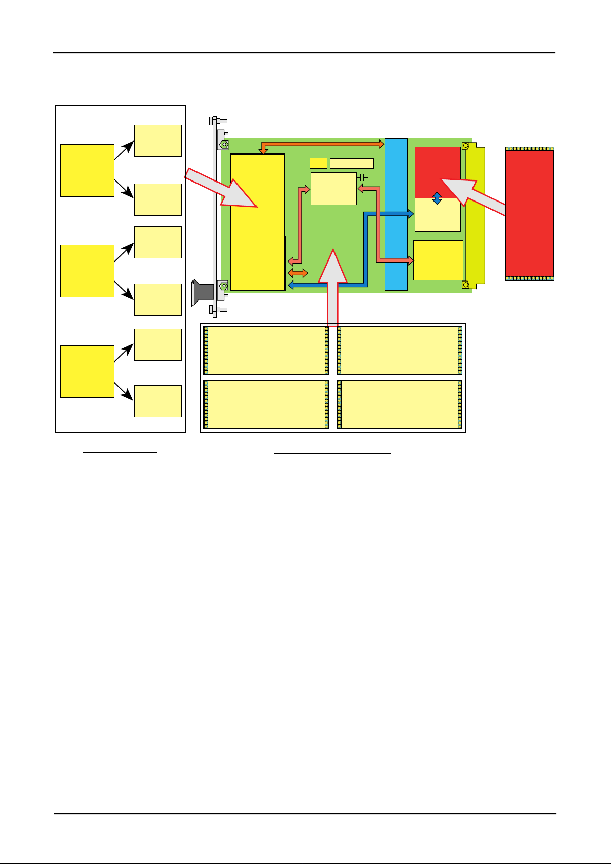
Figure 1.2.0.1: VM62(A)/VM42(A) Configuration Options
SRAM
VM42(A)
MC68040
@ 33 MHz
MC68EN360
@ 33 MHz
VM42(A)
MC68040V
@ 33 MHz
MC68EN360
@ 33 MHz
256 kByte
OR
SRAM
1 MByte
SRAM
256 kByte
OR
SRAM
1 MByte
68EN360
* Ethernet
* 6 serial I/O
* Timers
* Watchdog
Companion Mode
VM62(A)
MC68060
@ 50 / 66MHz
VM42(A)
MC68040(V)
MC68040
@ 33 MHz
RTC
dual-ported
SRAM
DRAM
FLASH
1 kbit EEPROM
+
MP
interface
(optional)
Spanciever
CXC Interface
Dual-ported
SRAM
128 kByte
VMEbus
* System
controller
* Master/slave
interface
VMEbus
Optional MP
Interface Piggyback
VM62(A)
MC68060
@ 50/66 MHz
MC68EN360
@ 25 /33MHz
CPU Options
SRAM
256 kByte
OR
SRAM
1 MByte
Optional Memory Piggyback
with
1 MByte DRAM
1 MByte FLASH
Optional Memory Piggyback
with
16 MByte DRAM
1 or 4 MByte FLASH
Memory Piggybacks
Optional Memory Piggyback
with
4 MByte DRAM
1 or 4 MByte FLASH
Optional Memory Piggyback
with
32 MByte DRAM
512 kByte or 2 MByte FLASH
Page 1-4 © 1995 PEP Modular Computers May 17, 1996
Page 11

VM62(A) / VM42(A) User’s Manual Chapter 1 Introduction
1.3 Specifications
Main CPU
I/O Controller
Memory
DRAM
FLASH
SRAM
EEPROM
VMEbus Interface
A24:D16/D8
Arbitration
AM Codes
MC68060 66 or 50 MHz (3.3V)
MC68040 33 or 25 MHz
MC68040V 33 or 25 MHz (3.3V)
MC68LC040 33 or 25 MHz
MC68EN360, 25 or 33MHz used in companion mode
1, 4, 16 or 32 Mbyte
0.5, 1, 2, or 4 MByte
1 MByte or 256 kByte (dual-ported, backed-up using Gold-Caps)
2 kbit (serial); 1 kbit available for applications
Master and slave with optional AutoBahn Interface (100 MBytes/sec)
Single level (BR3*), release-when-done daisy-chain
Standard Superv./User Prog./Data HEX 39/3A/3D/3E
User Defined HEX 10-17/18-1F
Short I/O HEX 29/2D
System controller functions
• Automatic First Slot Detection (FSD)
• SYSRES* (disabled by jumper)
• SYSCLK* (disabled by jumper)
• ACFAIL*
• SYSFAIL*
• Power monitor
• Bus monitor (programmable)
• VME IRQ mask register
A24:D16
Dual-port SRAM
1 Mailbox IRQ
Interrupt Control
7 Level VME IRQ Handler,
maskable via VME IRQ mask
register
System vectors
* Available for Index 02 boards or later.
Slave
1 Mbyte window, software programmable base (1 out of 16 addresses)
Lower 8kBytes of the SRAM area
ACFAIL* -> Level 7 autovectored
ABORT -> Level 7 autovectored
TICK -> Level 6 autovectored
SYSFAIL* -> Level 3 autovectored (maskable)
Mailbox IRQ -> Level 5 autovectored
AutoBahn IRQ 2 -> Level 2 autovectored
AutoBahn IRQ 1 -> Level 1 autovectored
16 on-board Interrupters, Levels / Vectors programmable
*
May 17, 1996 © 1995 PEP Modular Computers Page 1-5
Page 12

Chapter 1 Introduction VM62(A) / VM42(A) User’s Manual
I/O Ports
Serial
Mezzanine Interface
Timers
RISC controller (in the 68EN360) with 14 dedicated DMA channels
4*multiprotocol SCCs up to 8 MBaud
with one (two) supporting IEEE 802.3/Ethernet up to 10 Mbit/s
10Base5, 10Base2 or 10BaseT
2*UARTs RS232 (XON/XOFF) RS232 up to 120 kBaud
4 independent baud rate generators
CXC Interface
- 16 bit asyncronous data transfer with 4 IRQs,
independent DMA channel
- 3 serial interfaces
TICK
General Purpose
Watchdog
Special Functions
Real-time clock (backed-up)
Serial EEPROM
DMA
Front Panel Functions
Data Retention
Short term backup for RTC and
SRAM via on-board Gold-Cap
Periodic Interrupt Timer, programmable
4*16 bit or 2*32 bit, programmable
512 ms time-out for reset, programmable
Date (year, month, week, day)
Time (hour, minute, second)
1 kbit for board specific data (serial number, Internet address, etc.)
+ 1 kbit for application purposes
2 independent channels (supports single and dual address transfers
between all offboard locations including DRAM, FLASH,
AutoBahn memory, CXC and VME)
RESET button
ABORT button
HALT LED (red)
Watchdog LED (yellow)
General purpose LED (green)
Typ. 2µA/3V -> 50 hours
Long term backup via VME 5V
Stby line
Power Requirements
VM62 /66 MHz
VM62 /50 MHz
VM42 /33 MHz (68040)
VM42 /25 MHz 3.3V (68040V)
Temperature Range
Operating Humidity
Board Size
VMEbus Connector
Front panel width
Page 1-6 © 1995 PEP Modular Computers May 17, 1996
Dependent on the battery installed on the system 5V Stby.
Automatic switching between 5V Stby and internal Gold-Cap
Typ. 30µA/3V
To be defined
5 W with DM600 and SITB5 fitted
7W with DM600 and SITB5 fitted
4 W with DM600 and SITB5 fitted
Standard 0 - 70˚C
Optionally E2 -40˚C to +85˚C
0 to 95% non-condensing
Single height Eurocard 100*160 mm
DIN 41612 style C, 96 contacts, P1 connector
4 TE, 1 slot
Page 13
VM62(A) / VM42(A) User’s Manual Chapter 1 Introduction
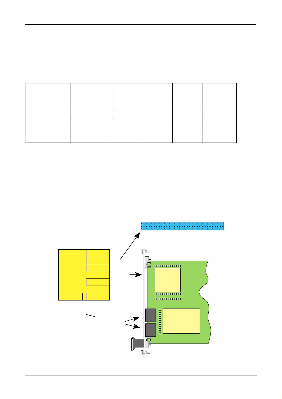
1.4 Features
CPU Options
The Table below illustrates the capabilities of the available CPUs. The 68060 processors operating at 50 MHz deliver up
to 100 MIPs while the 68040 processors operating at 33 MHz give performances up to 35 MIPs.
Table 1.4.0.1: CPU Configuration
Processor Product CPU MMU FPU Supply
MC68040 VM42(A) √ √ √ 5V
MC68LC040
MC68040V VM42(A) √ √ 3.3V
MC68060 VM62(A) √ √ √ 3.3V
*
VM42(A) √ √ 5V
MC68EC060
planned project
*
68EN360
25/33 MHz - the ‘QUICC’ chip used in ‘companion mode’ is tightly coupled to the CPU. Working as an I/O and system
controller, it provides all the necessary interfaces, timers and clocks etc. in addition to the DRAM memory controller.
Serial Channels
Six are provided by the ‘QUICC’ - Two SMC channels are ported to the front panel and the remaining four SCC channels
may be optionally configured as shown below.
Figure 1.4.0.2: MC68EN360 Intelligent Controller Schematic
Mask E71M required.
MC68EN360
VM62(A)
SCC2
SCC3
SCC4
SCC1
}
}
√
SI-Interface
3.3V
CXC Interface
SI-Piggyback
Interface
}
SMC2SMC1
2x RS232 with
Rx and Tx only
May 17, 1996 © 1995 PEP Modular Computers Page 1-7
Memory
Piggyback
Page 14

Chapter 1 Introduction VM62(A) / VM42(A) User’s Manual
Ethernet Interface (SI-10B2, SI-10B5, SI-10BT)
Three different piggybacks complete with all the associated control logic are available providing 10Base5, 10Base2 or
10BaseT interfaces.
Note
The SI-10B5 piggyback requires an external +12V power source to operate.
Fieldbus Interface (SI-PBPRO)
This is a fully optoisolated RS485 (PROFIBUS) interface piggyback with a 9-pin D-Sub connector.
RS232 Serial Interface
Two piggybacks are available with RJ45 connectors for MODEM compatible communication.
AutoBahn Interface (MP-AB100)
This is realised via a piggyback containing all the necessary control logic, 128 kByte high speed SRAM (10 ns) as a
memory buffer between the processor and the AutoBahn chip (MC 100SX1451) for communication on the high speed
serial data lines over pins b21 and b22 of the VMEbus.
DMA Channels
2 independent channels are provided by the ‘QUICC’ chip and can be used by applications requiring data transfer between
CXC-modules, DRAM, FLASH memory, dual-ported SRAM and AutoBahn memory buffers. This memory can be
configured with different memory options allowing tremendous flexibility when customising memory requirements for
real-time applications.
DRAM/FLASH
This memory, complete with a 32 bit data wide access bus is placed on a piggyback with addressing capability for up to
two memory banks of 64 MByte each. On-board +5V FLASH memory provides the latest ROM technology allowing the
user to take advantage of the on-board programming facility to produce low cost upgrades by simply overwriting existing
stored data.
SRAM
This is a dual-ported battery-backed (Gold-Cap) memory area with a 16 bit data wide access bus. Users of the VMEbus
and the on-board CPU both have access to this memory. The lower 8 kByte are reserved for the location monitor.
EEPROM
Although a 2 kbit EEPROM is provided on-board, 1 kbit has been pre-programmed with PEP production data (boot info,
Ethernet registration, etc) leaving the remaining 1 kbit for user application code. A write protect jumper prevents
accidental erasure.
Page 1-8 © 1995 PEP Modular Computers May 17, 1996
Page 15

VM62(A) / VM42(A) User’s Manual Chapter 1 Introduction
1.5 Related Publications
VITA
VMEbus Specifications Revision C1
MPI: Modpack and CXC Specification from PEP (Version 1.5 or later)
Motorola
M68060 Microprocessors User’s Manual
M68040 Microprocessors User’s Manual
MC68EN360 Quad Integrated Communications Controller User’s Manual
AutoBahn Spanceiver Data Sheet
EM Microelectronic
V3021 1 Bit Real Time Clock Data Sheet
XICOR
X25C02 SPI Serial EEPROM Data Sheet
May 17, 1996 © 1995 PEP Modular Computers Page 1-9
Page 16
VM62(A) / VM42(A) User’s Manual Chapter 2 Functional Description
2
2. FUNCTIONAL DESCRIPTION
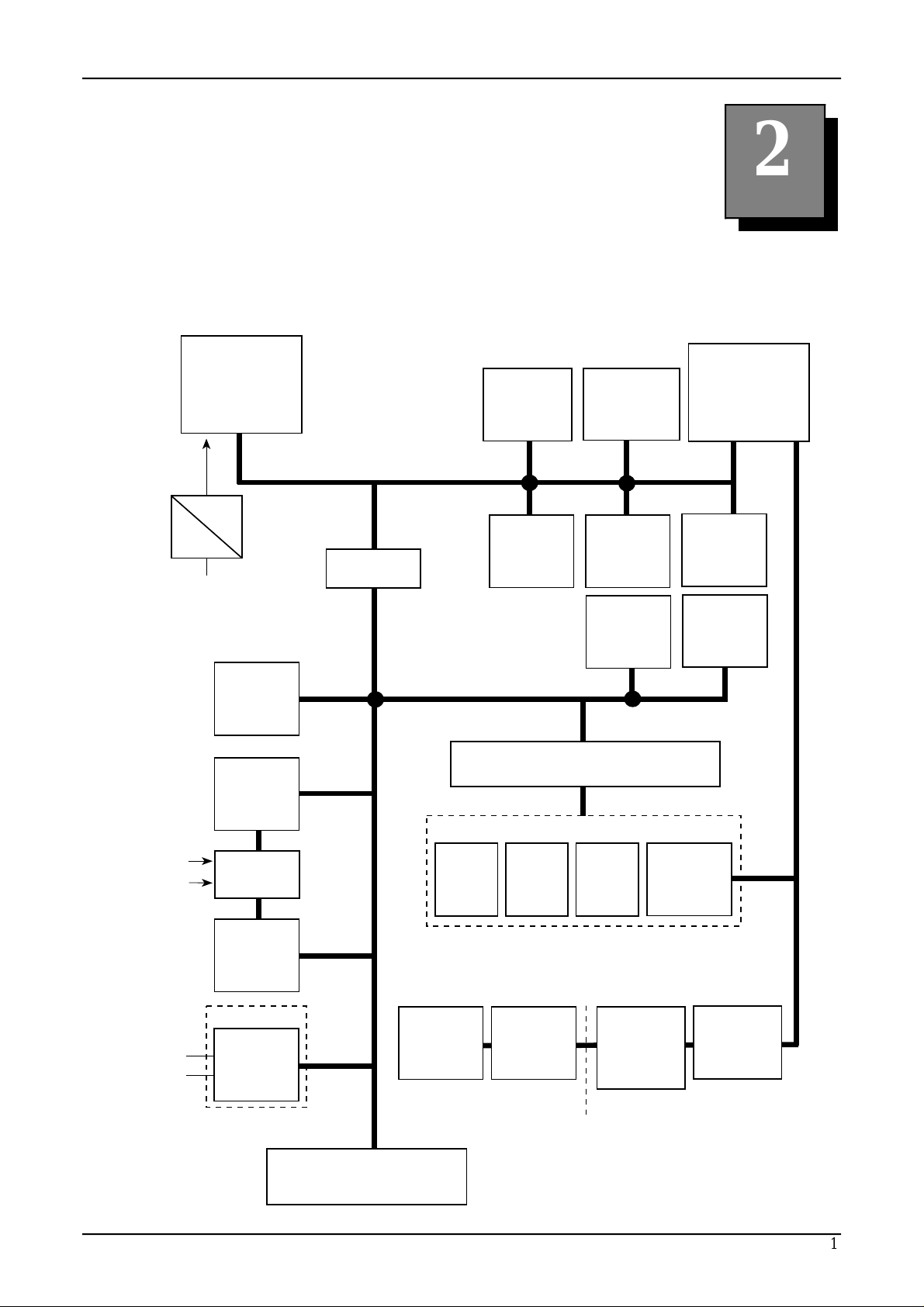
Figure 2.0.0.1: VM62(A) / VM42(A) Block Diagram
CPU
68(LC)040
68040V
33 / (40) MHz
68060
50 / 66 / (80) MHz
3.3V
5V
Serial
EEPROM
Real-Time
Clock
Address/
Data/
Control
BUSSIZER
SPI
1 Bit
1 Bit
32 Bit 32 Bit
DRAM
1/4/16/32 MB
IRQ
Handler
CXC (Serial / Parallel / DMA Port)
16 Bit
FLASH
0.5/1/2/4 MB
Clock
Logic
Status/
Control
Logic
8 Bit
68EN360
Companion
Mode
25/33/(40) MHz
Reset
Logic
Watchdog
optional
On board Gold-Cap
VME 5V Stdby
b21
b22
Backup
Logic
Dual-Port
SRAM
256/1MB
70ns
optional
AutoBahn
Interface
autoswitchover
16 Bit
32 Bit
VMEbus Interface
Master / Slave
Serial
I/O User
Spec
SCC2
Serial
I/O
RS232
SMC1
16 Bit
Serial
I/O User
Spec
SCC3
Serial
I/O
RS232
SMC2
Standard I/O Additional I/O
Serial
I/O User
Spec
SCC4
Front Panel
10Base2/5/T
RS485
RS232 ISo
2*RS232
SCC1 SCC4
SCSI
(DMA)
LED
Functions
May 17, 1996 © 1995 PEP Modular Computers Page 2-1
Page 17

Chapter 2 Functional Description VM62(A) / VM42(A) User’s Manual
2.1 The 68EN360 (QUICC) on the VM62(A) / VM42(A)
Motorola’s MC68EN360 is a 32 bit high performance communication controller, combining powerful peripheral
functions with system integration functions and an on-chip microprocessor core (CPU32+).
On the VM62(A) / VM42(A), the on-chip CPU core is disabled and replaced with a more powerful external CPU, the
MC68040 or MC68060. The 68EN360 operates as a slave to the CPU in so-called ‘Companion Mode’. In this mode, the
68EN360 provides complete I/O functionality. The DMA channels can still obtain ownership of the CPU’s system bus
and therefore all on-chip DMA channels can address the whole of the address space. Moreover, important functions for
system integration, such as memory controller, clock generation, interrupt controller etc. are available in this mode,
meeting the requirements for the initialisation of the 68EN360, described later in this manual.
The programming of the 68EN360 begins by determining the block of on-chip RAM and registers via the MBAR
register. This register is located at a fixed address and can only be accessed in CPU space.
2.2 Address Decoder
2.2.1 Basic Structure
The address decoder of the VM62(A) / VM42(A) consists of two basic parts. A primary address decoder pre-decodes the
select signals for the processor data bus (in front of the bussizer) and for the I/O data bus (behind the bussizer). With
reference to initial boot cycles, the primary address decoder passes or enables a secondary address decoder stage. The
secondary address decoder stage is realised using the programmable chip slect logic of the MC68EN360. The 8 outputs of
the 68EN360 chip select logic are used for the base addresses of the various memory and I/O address ranges.
2.2.2 Boot Decoding
Due to the fact that the default boot memory used by the VM62(A) / VM42(A) is FLASH memory, which is completely
reprogrammable, a special boot decoder is provided. The boot memory is jumper selectable, the user having the choice
between FLASH (default), VMEbus memory or the on-board AutoBahn Interface. The boot decoder redirects the physical
address range 0H to 1000000H from either FLASH (DM60x), VMEbus or MP piggyback, providing the selected boot
memory is initially accessed.
Note
VMEbus boot memory must be located at VME base address 0H in Standard Supervisor Program/Data
address space.
Page 2-2 © 1995 PEP Modular Computers May 17, 1996
Page 18

VM62(A) / VM42(A) User’s Manual Chapter 2 Functional Description
2.2.3 Primary Address Decoder
The primary address decoder generates the following select signals.
CS_360 Secondary address decoder (68EN360, DRAM, FLASH)
CS_VME VMEbus address range
CS_AUT AutoBahn Interface address range
CS_BSS Bussizer address range (VME, SRAM, AutoBahn, I/O)
BERR_0 Reserved address range (Bus Error)
EN_BSS 68EN360 DMA address range
IACK Interrupt Acknowledge Cycle
2.2.4 Secondary Address Decoder
The secondary address decoder is built by the 68EN360 chip select logic and is therefore programmable. The outputs are
used as base address selects, as shown below.
68EN360 Chip Select Connected to
CS0 FLASH
CS1 DRAM
CS2 VME via 68EN360 DMA
CS3 AutoBahn Interface
CS4 SRAM
CS5 CXC
CS6 RTC
CS7 Control / Status Registers
May 17, 1996 © 1995 PEP Modular Computers Page 2-3
Page 19
Chapter 2 Functional Description VM62(A) / VM42(A) User’s Manual
2.2.5 Address Map
The VM62(A) / VM42(A) address map shown in the Table below is based on the recommended default initialisation of
the 68EN360 chip select logic.
Figure 2.2.5.1: VM62(A) / VM42(A) Address Map (PEP Default)
Address (Hex) Device
00 xx xx xx
04 xx xx xx
07 00 0x xx
09 xx xx xx
0A xx xx xx
0B xx xx xx
0C xx xx xx
0D xx xx xx
1x xx xx xx
2x xx xx xx
3x xx xx xx
4x xx xx xx
5x xx xx xx
6x xx xx xx
82 xx xx xx
83 xx xx xx
85 00 xx xx
87 xx xx xx
87 xx xx xx
9x xx xx xx
Ax xx xx xx
Bx xx xx xx
C0 xx xx xx
C4 xx xx xx
C7 xx xx xx
CA xx xx xx
CB F7 0x xx
CC xx xx xx
CD 00 00 01
CD 00 00 05
CD 00 00 07
Dx xx xx xx
Ex xx xx xx
Fx xx xx xx
DRAM (68EN360’s CS1)
FLASH (68EN360’s CS0)
Reserved, 68EN360 internal RAM / register
DMA AutoBahn (CS3)
Reserved, mirrored 68EN360’s CS4
Reserved, mirrored 68EN360’s CS5
Reserved, mirrored 68EN360’s CS6
Reserved, mirrored 68EN360’s CS7
Reserved (BERR_0)
Reserved (BERR_0)
Reserved (BERR_0)
MP interface (CS_AUT)
Reserved (BERR_0)
Reserved (BERR_0)
The following address area is non-cachable serialised.
VMEbus (CS_VME), user-defined AM code
VMEbus (CS_VME), user-defined AM code
VMEbus (CS_VME), short I/O AM code
VMEbus (CS_VME), user-defined AM code
DMA-VME, 68EN360’s CS2
Reserved (BERR_0)
Reserved (BERR_0)
Reserved (BERR_0)
Reserved, mirrored DRAM
Reserved, mirrored FLASH
Reserved, 68EN360 internal RAM / register
68EN360’s CS4, SRAM
68EN360’s CS5, CXC
68EN360’s CS6, RTC
68EN360’s CS7+1, VME IRQ MASK register
68EN360’s CS7+5, VME control / status register
68EN360’s CS7+7, board control / status register
Reserved (BERR_0)
Reserved (BERR_0)
Reserved (BERR_0)
Note
In order to determine the base of the 68EN360’s internal memory map, the module base address register
(MBAR) must be set. The location of this register is fixed in the address area Supervisor CPU Space at
3FF00H. For more information, please refer to the Software Configuration chapter in this manual.
Page 2-4 © 1995 PEP Modular Computers May 17, 1996
Page 20

VM62(A) / VM42(A) User’s Manual Chapter 2 Functional Description
2.2.6 DMA Transfers
Memory to memory transfers with the 68EN360 DMAs are possible with any combination of on-board and VME
addresses. In order to achieve address compatibility between CPU/VME and DMA/VME transfers, it is recommended that
the initialisation of CS2 be initialised to the standard VME address space as described in the Software Configuration
chapter in this manual.
2.3 VMEbus Interface
The VM62(A) / VM42(A) has a complete master interface for the P1, J1 VMEbus connector. It consists of a VMEbus
arbiter, requester, system controller and buffers for data/address/control signals. In addition, the VM62(A) / VM42(A)
provides a VMEbus slave interface which consists of a programmable board address decoder, a dual-ported RAM and a
mailbox interrupt controller.
2.3.1 System Controller
The VM62(A) / VM42(A) can act as a VME system controller with arbiter, system clock driver, power monitor with
system reset driver, IACK daisy chain driver and 7-level VMEbus interrupt controller.
Arbitration is single level FAIR1 on BR3*. If the VM62(A) / VM42(A) is used as system controller it has to be placed
in slot 1 of the VMEbus backplane (furthermost left slot). There is no jumper setting necessary, as the board provides a
‘first slot detection’ function which is also readable within the VME control / status register. The IACK daisy chain
driver is supplied by connecting the IACKIN* and IACKOUT* line. IACK* is connected via the VMEbus backplane for
IACKIN* of slot 1.
VME SYSCLK* and SYSRES* can be routed from on-board using jumpers, leaving the choice of generating these
signals by the system controller to the user. SYSFAIL* generates a maskable on-board autovectored interrupt (see also
External Autovector Requests). ACFAIL* generates a non-maskable autovector level 7 interrupt (NMI) in the same way
as the ABORT button. When an ACFAIL* NMI is detected, it can be differentiated from an ABORT by reading bit 1 of
the Board Control/Status Register (bit 1 is set to ‘1’ for ACFAIL*). If this is the case, the CPU should stay in the IRQ
service routine and save any important data to non-volatile memory.
The VM62(A) / VM42(A) also provides a bus monitor for the VMEbus. A 128µs timeout timer monitors VMEbus data
transfer cycle lengths and generates a VMEbus BERR* signal for error termination. This timer is enabled/disabled via the
VME control / status register which also supplies a timeout status bit in order to identify bus errors generated by the bus
monitor.
2.3.2 Dual-Ported SRAM
The VM62(A) / VM42(A) provides on-board SRAM of either 256 kByte or 1 Mbyte. The SRAM is 16- bit wide and
dual-ported between the CPU/DMA and VME, accessible through an on-board arbiter. Read-Modify-Write cycles (TAS
instruction used for semaphores) are supported in any direction. The location of the dual-ported SRAM as seen from the
VME is programmable via the VME control / status register. There are 16 different base addresses possible that are all
located in the VME standard supervisor / user data space. Enable / disable is selected using a separate bit.
Note
The lower 8 kBytes of dual-ported SRAM should not be accessed from the VME because this area is
reserved for mailbox interrupts.
1
FAIR according to VME 64 Specifications, Rule 3.14 and Observation 3.17.
May 17, 1996 © 1995 PEP Modular Computers Page 2-5
Page 21

Chapter 2 Functional Description VM62(A) / VM42(A) User’s Manual
2.3.3 Mailbox Interrupt
An external VMEbus master may interrupt the VM62(A) / VM42(A) by setting P_IRQ5 (pending mailbox IRQ) in the
VME control / status register. The address of this dual-ported register seen from VME is identical to the base address of
the dual-ported SRAM, occupying the lower 8 kBytes (odd byte addresses) of the dual-ported SRAM.
Setting P_IRQ5 generates an autovector 5 interrupt on the CPU. Typically, the on-board CPU resets P_IRQ5 during the
processing of the corresponding interrupt service routine.
Note
Although every odd address of the 8k block of the VME control / status register can be accessed from
VME, only the P_IRQ5 bit can be set. All other bits are write protected from the VME. As the
P_IRQ5 bit is located at bit 7 within the register, it can be directly used as a semaphore because readmodify-write (TAS instruction) is supported.
2.3.4 VMEbus Control / Status Register
Address: CS7 + $5 PEP Default Address $CD 00 00 05
Format: Byte
Access: read / write
Value after HW reset: see table
CS7 + $5
P_IRQ5 FSDEN_BERR2EN_DPR
BADR2BADR3 BADR1 BADR0
Register Description
Name Value Reset (HW) Reset PEP (SW) Description
Slot 1 Other Slot 1 Other
P_IRQ5
1 0 0 0 0 Pending mailbox IRQ
bit 7
EN_DPR
bit 6
1 0 0
Value
stored in
EEPROM
Value
stored in
EEPROM
Dual-port RAM (including mailbox
IRQ) for VME requester enabled. Base
address fixed through BADRx bits
EN_BERR2
bit 5
FSD
bit 4
BADR3
- BADR0
bits 3 - 0
1 0 0 1 0 Enable bus monitor timer, all VME
cycles, timeout after 128µs
1 1 0 1 0 VMEbus ‘First Slot Detection’ flag,
system controller
0 0
Value
stored in
EEPROM
Value
stored in
EEPROM
VME address location of dual-ported
RAM. Equivalent to VME address lines
A23 - A20, programmable from $0 - $F
in 1 Mbyte windows, enabled with
EN_DPR. See Table on next page.
01234567
Page 2-6 © 1995 PEP Modular Computers May 17, 1996
Page 22

VM62(A) / VM42(A) User’s Manual Chapter 2 Functional Description
BADR [3 .. 0] VME Board Base Address
0000
0001
0010
0011
0100
0101
0110
0111
1000
1001
1010
1011
1100
1101
1110
1111
$00 00 00
$10 00 00
$20 00 00
$30 00 00
$40 00 00
$50 00 00
$60 00 00
$70 00 00
$80 00 00
$90 00 00
$A0 00 00
$B0 00 00
$C0 00 00
$D0 00 00
$E0 00 00
$F0 00 00
2.4 Interrupt Control
The interrupt control logic processes internal interrupt requests (68EN360), together with external requests (VME) and
external autovectored interrupt requests. The interrupt control logic is built up using the 68EN360 internal interrupt
controlling and a 7-level VMEbus interrupt handler with the corresponding mask register.
2.4.1 Internal Requests
Internal requests are related to all interrupt requests caused by the 68EN360 sources, including the 68EN360 system
integration functions (watchdog timer, periodic interrupt timer) and the communication processor module (RISC
controller, timers, DMAs, SCCs and so on). For more information, please refer to the 68EN360 User’s Manual.
In order to avoid conflicts regarding interrupt levels, it is recommended to use IRQ level 4 for 68EN360 CPU internal
requests and IRQ level 6 for 68EN360 SIM60 internal requests.
Note
The 4 IRQ lines specified by CXC are supplied by the 68EN360 Port C lines and are therefore also
processed as internal requests (PC0, 1, 2, 3).
2.4.2 External Autovector Requests
Some 68EN360 external interrupt sources are routed to the IRQ lines of the 68EN360 and generated as autovectored
interrupts. Care must be taken that the relevant 68EN360 register is initialised with respect to the wiring (see also the
Software Configuration chapter in this manual).
Source 68EN360 Pin Autovector
ABORT / ACFAIL IRQ7 7
TICK IRQ6 6
Mailbox IRQ IRQ5 5
SYSFAIL IRQ3 3
AutoBahn IRQ2 IRQ2 2
AutoBahn IRQ1 IRQ1 1
May 17, 1996 © 1995 PEP Modular Computers Page 2-7
Page 23

Chapter 2 Functional Description VM62(A) / VM42(A) User’s Manual
2.4.3 VME Interrupt Mask Register
Address: CS7 + $1 PEP Default Address $CD 00 00 01
Format: Byte
Access: read / write
Value after HW reset:0
Value after PEP SW initialization: Value of EEPROM
01234567
CS7 + $1
Register Description
Name Value Description
EN_IRQx 1 Enable VME IRQx where x = 1 to 7
SYSFAIL 1 Enable VME SYSFAIL IRQ autovector 3
EN_IRQ7 EN_IRQ4EN_IRQ5EN_IRQ6
EN_IRQ2EN_IRQ3 EN_IRQ1 SYSFAIL
Page 2-8 © 1995 PEP Modular Computers May 17, 1996
Page 24

VM62(A) / VM42(A) User’s Manual Chapter 2 Functional Description
2.5 I/O Ports
2.5.1 Ethernet Port
The MC68EN360 is specified to support a full set of IEEE 802.3/Ethernet CSMA/CD media access control and channel
interface functions. Since the 68EN360 requires an external interface adapter and transceiver function, the Ethernet port
can be adapted to all standard Ethernet functions, such as 10BaseT, 10Base5 and 10Base2 via a piggyback connected to the
SI Interface on the VM62(A) / VM42(A).
2.5.2 Serial Ports
The VM62(A) / VM42(A) provides 6 serial ports based on the 68EN360 communications processor. The ports can be
configured in the following way:
• 2 * service / debug ports (SMC port / RxD / TxD only RS232);
• 4 * full MODEM ports / multiprotocol channels (SCC ports).
The service / debug ports are configured as default on the VM62(A) / VM42(A). These ports supply RxD/TxD RS232
Interfaces software handshake (XON/XOFF) capability. The full MODEM ports supply RxD, TxD, RTS, CTS, CD,
DTR and RCLK/TCLK. Two of the full MODEM ports can be configured on the SI Interface with a variety of SI
Modules (RS232/RS485, isolated/non-isolated and so on). Together with the two service/debug ports, a maximum of
three (four) completely configured serial ports are available for the base board. Three (two) serial ports may be configured
via the CXC where three of the four full MODEM Interfaces are routed.
Figure 2.5.2.1: MC68EN360 Intelligent Controller Schematic
CXC Interface
SCC2
SCC3
}
}
Rx and Tx only
SI-Interface
SI-Piggyback
Interface
MC68EN360
}
SCC4
SCC1
SMC2SMC1
2x RS232 with
Memory
Piggyback
Note
The serial channel SCC4 is routed to both the SI Interface and the CXC and can only be used by one or
the other and not both at the same time.
May 17, 1996 © 1995 PEP Modular Computers Page 2-9
Page 25

Chapter 2 Functional Description VM62(A) / VM42(A) User’s Manual
The Ethernet port can be configured via the SI Interface with 10BaseT, 10Base5 or 10Base2 SI Modules. The following
configurations are therefore possible for the serial ports.
Versions with Ethernet Port
Port 68EN360 Resource Configured via
Service/Debug 1 SMC1 Base board, upper RJ12
Service/Debug 2 SMC2 Base board, lower RJ12
Ethernet SCC1 Base board, SI Module
Full MODEM 2 SCC2 CXC Module
Full MODEM 3 SCC3 CXC Module
Full MODEM 4 SCC4 CXC Module
*
The 10BaseX Modules do not make use of SCC4 and, therefore, can be used on the CXC.
Versions without Ethernet Port
Port 68EN360 Resource Configured via
*
Service/Debug 1 SMC1 Base board, upper RJ12
Service/Debug 2 SMC2 Base board, lower RJ12
Full MODEM 1 SCC1 Base board, SI Module
Full MODEM 2 SCC2 CXC Module
Full MODEM 3 SCC3 CXC Module
Full MODEM 4 SCC4 Base board, SI Module or CXC Module
*
Can only be used once.
*
2.5.3 CXC Interface
The Controller Extension Connector (CXC) is a local mezzanine interface. The CXC contains a 16-bit data bus, 7 address
lines and 8 decoded chip select lines. In total, there are 8 control signals. The base address of the CXC can be programmed
via the CS5 line of the 68EN360. The 8 CXC chip selects (CXC_CS0 - CXC_CS7) occupy 256 Bytes each and have an
address length of 400H (512 Bytes).
Furthermore, the CXC contains 4 IRQ capability (4 edge sensitive IRQs), DMA capability (1 channel, DREQ + DACK),
serial ports (3 channels, Full MODEM) and a set of parallel port signals. These special CXC functions are based on the
68EN360 resources.
For general CXC information, including generic pinouts and a comparison of the 68(EN)360 and 68302 CPU pinouts on
the CXC, please refer to the CXC Specification User’s Manual and the CXC Appendix attached to this manual.
Page 2-10 © 1995 PEP Modular Computers May 17, 1996
Page 26

VM62(A) / VM42(A) User’s Manual Chapter 2 Functional Description
Table 2.5.3.1: CXC Pinouts using the 68(EN)360
Pin Row A
Signals
1 PC0/_RTS1/L1ST1 PA8/CLK1/BRGO1/L1RCLKA/TIN1 PB6/SMTXD1/_DONE1
2 PC1/_RTS2/L1ST2 PA10/CLK3/BRGO2/L1TCLKA/TIN2 PB5/BRGO2/_DACK1
3 PC2/_RTS3/_L1RQB/L1ST3 GND PB4/BRGO1/_DREQ1
4 PC3/_RTS4/_L1RQA/L1ST4 PA3/TXD2 PB11/SMRXD2/L1CLKOA
5 PB0/_SPISEL/_RRJCT1 PB13/_RTS2/L1ST2 PA14/CLK7/BRGO4/TIN4
6 PB1/SPICLK/_RSTRT2 GND PA15/CLK8/_TOUT4/L1TCLKB
7 VCC PB15/_RTS4/_L1RQA/L1ST4 VCC
8 PB2/SPIMOSI(SPITXD)/_RRJCT2 PC11/_CD4/_L1RSYNCA PA7/TXD4/L1RXDA
9 PB3/SPIMISO(SPIRXD)/BRGO4 GND PA6/RXD4/L1TXDA
10 PB8/_SMSYN1/_DREQ2 PA2/RXD2 PB7/SMRXD1/_DONE2
11 PB16/BRGO3/STRBO PB10/SMTXD2/L1CLKOB PC9/_CD3/_L1RSYNCB
12 PB9/_SMSYN2/_DACK2 GND PB14/_RTS3/_L1RQB/L1ST3
13 PB17/_RSTRT1/STRBI PC6/_CTS2 PC8/_CTS3/_L1TSYNCB/SDACK2
14 VCC PC7/_CD2/_TGATE2 VCC
15 _CS-CXC (CS5 of 68360) GND PA12/CLK5/BRGO3/TIN3
16 _AS PC10/_CTS4/_L1TSYNCA/_SDACK1 PA13/
17 R/_W _SYSR PA5/TXD3/L1RXDB
18 _UDS GND PA4/RXD3/L1TXDB
19 _LDS _EDTACK VCC
20 VCC 16MHz CLOCK _CXC-CS2
21 A1 GND _CXC-CS3
22 A2 _CXC-CS0 _CXC-CS4
23 A3 _CXC-CS1 _CXC-CS5
24 A4 GND _CXC-CS6
25 A5 A6 _CXC-CS7
26 VCC A7 VCC
27 D0 GND D10
28 D1 D6 D11
29 D2 D7 D12
30 D3 GND D13
31 D4 D8 D14
32 D5 D9 D15
Row B
Signals
Row C
Signals
CLK6/_TOUT3/L1RCLKB/BRGCLK2
May 17, 1996 © 1995 PEP Modular Computers Page 2-11
Page 27

Chapter 2 Functional Description VM62(A) / VM42(A) User’s Manual
CXC
Function
IRQ_1 a1 Yes PC0
IRQ_2 a2 Yes PC1
IRQ_3 a3 Yes PC2
IRQ_4 a4 Yes PC3
CXC
Function
DMA_ACK c2 Yes PB5
DMA_REQ c3 Yes PB4
CXC
Function
SER1_RCLK b1 Yes PA8
Pin Nr. 68302 HW
Compatible
Pin Nr. 68302 HW
Compatible
Pin Nr. 68302 HW
Compatible
68(EN)360
Port
68(EN)360
Port
68(EN)360
Port
Comment
Comment
Comment
SER1_TCLK b2 Yes PA10
SER1_TXD b4 Yes PA3
SER1_RXD b10 Yes PA2
SER1_RTS b5 Yes PB13
SER1_DTR a13 Yes PB17
SER1_CTS b13 Yes PC6
SER1_CD b14 Yes PC7
CXC
Function
SER2_RCLK c16 Yes PA13 Cannot be used if J6 is set
SER2_TCLK c15 Yes PA12
SER2_TXD c17 Yes PA5
SER2_RXD c18 Yes PA4
SER2_RTS c12 Yes PB14
Pin Nr. 68302 HW
Compatible
68(EN)360
Port
Comment
See note 3
SER2_DTR a11 Yes PB16
SER2_CTS c13 Yes PC8
SER2_CD c11 Yes PC9
Page 2-12 © 1995 PEP Modular Computers May 17, 1996
Page 28

VM62(A) / VM42(A) User’s Manual Chapter 2 Functional Description
CXC
Function
SER3_RCLK c6 Yes PA15 Not usable if SI Module uses SCC4
SER3_TCLK c5 Yes PA14
SER3_TXD c8 Yes PA7 Not usable if SI Module uses SCC4
SER3_RXD c9 Yes PA6 Not usable if SI Module uses SCC4
SER3_RTS b7 Yes PB15 Not usable if SI Module uses SCC4
SER3_DTR a12 Yes PB9 Not usable if SI Module uses SCC4
SER3_CTS b16 Yes PC10 Not usable if SI Module uses SCC4
SER3_CD b8 Yes PC11 Not usable if SI Module uses SCC4
Pin Nr. 68302 HW
Compatible
68(EN)360
Port
Comment
See note 4
See note 4
See note 4
See note 4
See note 4
See note 4
See note 4
CXC
Function
user defined a5 No PB0 Used on board SPI SEL for
Pin Nr. 68302 HW
Compatible
a6 No PB1 SPI Clk: can be used if an ‘SPI SEL’
a8 No PB2 SPI TxD: can be used if an ‘SPI SEL’
a9 No PB3 SPI RxD: can be used if an ‘SPI
a10 No PB8 See 68360 User Manual
b11 No PB10 Used on board SMC2 (Transmit)
c1 No PB6 Used on board SMC1 (Transmit)
c4 No PB11 Used on board SMC2 (Receive)
c10 No PB7 Used on board SMC1 (Receive)
68(EN)360
Port
Comment
EEPROM. Cannot be used on CXC
See note 2
other than PB0 is used.
other than PB0 is used.
SEL’ other than PB0 is used.
See note 1
See note 1
See note 1
See note 1
May 17, 1996 © 1995 PEP Modular Computers Page 2-13
Page 29

Chapter 2 Functional Description VM62(A) / VM42(A) User’s Manual
Notes
Reserved Pins
1) On a standard VM62(A)/VM42(A) board, these signals are already used for UART ports at BU7 and BU8.
2) On a standard VM62(A)/VM42(A) board, these signals are used for SPI to which the EEPROM is already
connected. PB0 is chip select of the EEPROM.
3) On PA13, a 24 MHz clock signal is routed via jumper J6. This signal is always needed for PEP standard
software (serial drivers).
Dual Functioning Signal Pins
4) These signals are routed both to the base board SI Interface connector (ST5C) and the CXC connector and can
only be used by one or the other and not both at the same time.
Due to this, a conflict exists if the SCC4 port is to be used with the SI232 piggyback and CXC boards (such as
CXM-SIO3), as both boards access this port. The SCC4 port can, therefore, not be used at the same time by SI
piggybacks and CXC boards.
The CXC ports SER1, SER2 and SER3 are equivalent to ports SCC2, SCC3 and SCC4 resp. on the 68xx360.
With regard to special CXC capabilities, the CXC pinout on the VM62(A) / VM42(A) has been developed to provide
maximum compatibility between the standard CXC functions. In addition, all signals are available in order to configure 2
time division multiplexed channels via the CXC (ISDN, PCM, GCI and so on). Multi-function pins with incompatible
functions with regard to the 68302 and 68EN360 (called user defined in the generic CXC specification) are not part of the
VM42(A) / VM62(A) CXC specification.
Although the SMCs are configured on the base board, these ports are also integrated on the CXC. This is because of
possible ISDN applications where SMCs can be integrated and other protocols supported by the 68EN360.
Note
If the RCLK2 signal (CXM pin c16) is required, jumper J6 (24 MHz clock) must be opened and the
serial drivers delivered by PEP modified.
Page 2-14 © 1995 PEP Modular Computers May 17, 1996
Page 30

VM62(A) / VM42(A) User’s Manual Chapter 2 Functional Description
Table 2.5.3.2: Further Explanation of 68(EN)360 Mnemonics
Group Signal Name Mneumonic Function
SCC Receive Data RXD4-RXD1 Serial receive data input to the SCCs (I)
Transmit Data TXD4-TXD1 Serial transmit data output from the SCCs (O)
Request to Send _RTS4-_RTS1 Request to send outputs indicate that the SCC is ready
to transmit data (O)
Clear to Send _CTS4-_CTS1 Clear to send inputs indicate to the SCC that data
transmission may begin (I)
Carrier Detect _CD4-_CD1 Carrier detect inputs indicate that the SCC should begin
reception of data (I)
Receive Start _RSTRT1 This output from SCC1 identifies the start of a receive
frame. Can be used by an Ethernet CAM to perform
address matching (O)
Receive Reject RRJCT1 This input to SCC1 allows a CAM to reject the current
Ethernet frame after it determines the frame address did
not match (I)
Clocks CLK8-CLK1 Input clocks to the SCCs, SMCs, SI, and the baud rate
IDMA DMA Request _DREQ2-
_DREQ1
DMA Acknowledge _DACK2-
_DACK1
DMA Done _DONE2-
_DONE1
TIMER Timer Gate _TGATE2-
_TGATE1
Timer Input TIN4-TIN1 Time reference input to the timer that allows it to
Timer Output _TOUT4-
_TOUT1
SPI SPI Master-In
Slave-Out
SPI Master-Out
Slave-In
SPI Clock SPICLK Output clock from the SPI master (O); input clock to
SPIMISO Serial data input to the SPI master (I); serial data
SPIMOSI Serial data output from the SPI master (O); serial data
generators (I)
A request (input) to an IDMA channel to start an
IDMA transfer (I)
An acknowledgement (output) by the IDMA that an
IDMA transfer is in progress (O)
A bidirectional signal that indicates the last IDMA
transfer in a block of data (I/O)
An input to a timer that enables/disables the counting
function (I)
function as a counter (I)
Output waveform (pulse or toggle) from the timer as a
result of a reference value being reached (O)
output from an SPI slave (O)
input to an SPI slave (I)
the SPI slave (I)
SPI Select _SPISEL SPI slave select input (I)
SMC SMC Receive Data SMRXD2-
SMRXD1
SMC Transmit Data SMTXD2-
SMTXD1
SMC Sync _SMSYN2-
_SMSYN1
May 17, 1996 © 1995 PEP Modular Computers Page 2-15
Serial data input to the SMCs (I)
Serial data output from the SMCs (O)
SMC syncronization signal (I)
Page 31

Chapter 2 Functional Description VM62(A) / VM42(A) User’s Manual
Group Signal Name Mneumonic Function
SI SI Receive Data L1RXDA,
L1RXDB
SI Transmit Data L1TXDA,
L1TXDB
SI Receive Clock L1RCLKA,
L1RCLKB
SI Transmit Clock L1TCLKA,
L1TCLKB
SI Transmit Sync
Signals
SI Receive Sync
Signals
IDL Interface
Request
SI Output Clock L1CLKOA,
SI Data Strobes L1ST4-L1ST1 Serial data strobe outputs can be used to gate clocks to
L1TSYNCA,
L1TSYNCB
L1RSYNCA,
L1RSYNCB
L1RQA, L1RQB IDL interface request to transmit on the D channel.
L1CLKOB
Serial input to the Time Division Multiplexed (TDM)
channel A or channel B
Serial output from the TDM channel A or channel B
Input receive clock to TDM channel A or channel B
Input transmit clock to TDM channel A or channel B
Input transmit data sync signal to TDM channel A or
channel B
Input receive data sync signal to TDM channel A or
channel B
Output from the SI
Output serial data rate clock. Can output a data rate
clock when the input clock is 2x the data rate
external devices that do not have a biult-in Time Slot
Assigner (TSA)
BRG Baud Rate Generator
Out 4-1
BRG Input Clock CLK2, CLK6 Baud rate generator input clock from which BRG will
PIP Port B 15-0 PB15-PB0 PIP Data I/O Pins
Strobe Out STRBO This input causes the PIP output data to be placed on
Strobe In STRBI This input causes data on the PIP data pins to be
SDMA SDMA
Acknowledge 2-1
2.5.4 AutoBahn Interface
In preparation
BRGO4-BRGO1 Baud rate generator output clock allows baud rate
generator to be used externally
derive the baud rates
the PIP data pins
latched by the PIP as input data
_SDACK2_SDACK1
SDMA output signals used in RISC receiver to mark
fields in the Ethernet receive frame
Page 2-16 © 1995 PEP Modular Computers May 17, 1996
Page 32

VM62(A) / VM42(A) User’s Manual Chapter 2 Functional Description
2.6 Special Functions
2.6.1 Real-Time Clock
The RTC (V3021 3-wire serial interface) is a 1-bit device which is accessible over the CS6 of the 68EN360. Its
timekeeping features include :-
• seconds, minutes, hours, day of month, month, year, week day and week number in BCD format.
• leap year and week number correction
• standby supply smaller than 1µA
See also the Software Configuration chapter in this manual and the V3021 data sheet.
2.6.2 EEPROM
The serial EEPROM is a 1-bit device which is accessible over the SPI Interface (3-wire Interchip) of the 68EN360. The
first half of the EEPROM (1 kbit) is reserved for factory data, including Board ID codes, Internet/Ethernet addresses, boot
information etc. The second half of the EEPROM is available for the user. See also the Software Configuration chapter in
this manual.
For more information on the EEPROM, please refer to the XICOR X25C02 data sheet.
2.6.3 TICK Generator
The 68EN360 internal Periodic Interrupt Timer is used by the PEP real-time operating system as TICK generator.
For more information please refer to the 68EN360 User’s Manual.
2.6.4 On-board Bus Error Timer
The VM62(A) / VM62(A) provides an on-board bus error timer. An 8µs timeout timer monitors the cycle lengths of data
transfers to and from locations beyond the bussizer, including on-board I/O, CXC, SRAM, AutoBahn and some VME.
After a timeout occurs, it generates an on-board BERR signal for error termination. This timer is enabled/disabled via the
board control/status register, which also supplies a timeout status bit in order to identify bus errors generated by the onboard bus error timer.
There are four cases of bus error.
Cause Timeout Enable / Disable possible
Reserved address BERR0
On-board BERR1
VME BERR2
Chip selects 68EN360
100ns
8µs
128µs
programmable
None
Yes, set in board control register
Yes, set in VMEbus control register
Yes, set in 68EN360 register
May 17, 1996 © 1995 PEP Modular Computers Page 2-17
Page 33

Chapter 2 Functional Description VM62(A) / VM42(A) User’s Manual
Note
During VMEbus cycles, the on-board bus error timer is reset as soon as the VM62(A) / VM42(A) gains
VMEbus ownership. This means that the time gap between a VMEbus request and the starting of the
VMEbus cycle is monitored by the on-board BERR timer. VMEbus cycles themselves are monitored
by the separate VMEbus BERR timer (BUS monitor).
2.6.5 VME Bus Error Timer
The VM62(A) / VM42(A) also provides a bus monitor for the VMEbus. A 128µs timeout timer monitors VMEbus data
transfer cycle lengths and generates a VMEbus BERR* signal for error termination. This timer is enabled/disabled via the
VME control/status register which also supplies a timeout status bit in order to identify bus errors generated by the bus
monitor.
2.6.6 Watchdog Timer
A 512ms watchdog timer triggers the on-board and VME system reset generator at timeout. Once enabled via the board
control/status register, the watchdog timer cannot be reset by software. It must be re-triggered via the corresponding bit in
the board control/status register periodically within the timeout period. ‘Watchdog timer running’ is a status that is
displayed by the yellow front panel LED.
Figure 2.6.6.1: Watchdog LED Location
Watchdog LED
Yellow
W
2.6.7 First Slot Detection (FSD)
The VM62(A)/VM62(A) detects during power-up whether the CPU in use is positioned in the far left slot of the system.
This is achieved using a 100k pull-down resistor at the BG3IN* pin.
BG3IN* low = system controller (far left slot)
BG3IN* high = no system controller
This information can be read from the VMEbus Control/Status register and is valid until the next power down of the
system.
Page 2-18 © 1995 PEP Modular Computers May 17, 1996
Page 34

VM62(A) / VM42(A) User’s Manual Chapter 2 Functional Description
2.6.8 Board Control/Status Register
Address: CS7 + $7 PEP Default Address $CD 00 00 07
Format: Byte
Access: read / write
Value after HW reset:0
01234567
CS7 + $7
Register Description
Name Value Access Description
WDG
bit 7
BERR2
bit 6
BERR1
bit 5
EN_WDG
bit 4
TR_WDG
bit 3
WDG EN_WDGBERR1BERR2
Read/Write Set by watchdog timer when timout has been reached. Used
to differentiate between resets caused by the watchdog and
resets caused by the reset button
(power up resets can be identified within the 68EN360)
Read/Write Set by VMEbus BUS monitor when timeout has been
reached. Used to identify BERR caused by this timer (see
also VMEbus Control/Status register)
Read/Write Set by on-board bus error timer when timeout has been
reached. Used to identify BERR caused by this timer
1 Read/Write Enable the watchdog timer. It can only be set once, and
remains enabled until the next reset
1 Read/Write Triggers the watchdog timer. Watchdog timeout = 512ms
EN_BERR1TR_WDG ACFAIL LED_G
EN_BERR1
bit 2
ACFAIL
bit 1
LED_G
bit 0
1 Read/Write Enables the on-board bus error timer. It also monitors all on-
board I/O cycles, including the time from the VMEbus
request to the VMEbus grant. Timeout = 8µs
1 Read/Write VME ACFAIL signal latched when active in order to
distinguish a level 7 NMI from an ABORT or ACFAIL
1 Read/Write Enables the green ‘general purpose’ front panel LED
Note
Information may be lost if the user writes to bit 7.
May 17, 1996 © 1995 PEP Modular Computers Page 2-19
Page 35

Chapter 2 Functional Description VM62(A) / VM42(A) User’s Manual
2.6.9 Reset Sources
Reset Source Identification
Push button No
SYSRES* VME No
Watchdog WDG bit on-board (Board Control/Status Register)
Power monitor (4.65V) Inside the 68EN360
2.7 Front Panel Functions
Figure 2.7.0.1: LED Port and Button Location
Watchdog LED
Yellow
General Purpose
Green
W
UH
RESET Switch ABORT Switch
RST AB
CPU HALT or RESET
Red
2.7.1 RESET Button
A RESET button is fitted to the front panel to avoid false operation. The RESET button triggers the on-board system reset
generator, as well as the VME if jumper J2 is set.
2.7.2 ABORT Button
Together with the RESET button, an ABORT button is also fitted to the front panel. The ABORT button generates a level
7 IRQ (non-maskable interrupt) which is used for debugging purposes. In this case, bit 1 of the Board Control/Status
Register is not set (remains ‘0’).
2.7.3 LED Port
The front panel LED port consists of three LEDs with the following functions:
Red LED CPU in HALT or RESET status
Yellow LED Watchdog timer running status
Green LED General purpose, set via board control/status register
The green LED is free to be used by the customer. It is set by the software during startup when the 68EN360 is initialized.
Page 2-20 © 1995 PEP Modular Computers May 17, 1996
Page 36

VM62(A) / VM42(A) User’s Manual Chapter 2 Functional Description
2.8 Data Retention for RTC and SRAM
Short term data retention for RTC and SRAM is gained with two Gold-Caps, each with a value of 0.22 Farad. In contrast
to Lithium cells, Gold-Caps do not require servicing. This short term backup is intended for short power failures or for
reconfiguring systems. An empty Gold-Cap needs approximately three hours to charge up, with backup times dependant on
the temperature, memory size and memory manufacturer tolerances. A well charged Gold-Cap provides a minimum of 10
hours backup time.
Laboratory tests at PEP indicate a typical backup time of 1 week for both 256kB and 1MByte SRAM plus RTC (typical
onboard backup current is 2µA.
Long term data retention is made via the VMEbus 5V Stby line. With respect to the VM62(A) / VM42(A), this voltage
can drop to 2.5V, with the typical current via the 5V Stby being 30µA at 3V.
Note
The VM42(A) / VM62(A) board can be removed from the system and then plugged in again without
losing any information. Data retention switches from the VME 5V Stby to the on-board Gold-Caps
automatically.
The on-board Gold-Caps are continuously reloaded via the 5V Stby line. The 5V Stby current is
typically 7mA for a few minutes when the Gold-Caps are at the beginning of the loading phase (fully
empty).
May 17, 1996 © 1995 PEP Modular Computers Page 2-21
Page 37

Chapter 2 Functional Description VM62(A) / VM42(A) User’s Manual
2.9 Register Overview
VME Interrupt Mask Register (page 2-8)
Address: CS7 + $1 PEP Default Address $CD 00 00 01
Format: Byte
Access: read / write
Value after HW reset:0
Value after PEP SW initialization: Value of EEPROM
01234567
CS7 + $1
VMEbus Control / Status Register (page 2-6)
Address: CS7 + $5 PEP Default Address $CD 00 00 05
Format: Byte
Access: read / write
Value after HW reset: see table on page 2-6
CS7 + $5
Board Control/Status Register (page 2-14)
Address: CS7 + $7 PEP Default Address $CD 00 00 07
Format: Byte
Access: read / write
Value after HW reset:0
EN_IRQ7 EN_IRQ4EN_IRQ5EN_IRQ6
P_IRQ5 FSDEN_BERR2EN_DPR
EN_IRQ2EN_IRQ3 EN_IRQ1 SYSFAIL
BADR2BADR3 BADR1 BADR0
01234567
01234567
CS7 + $7
Page 2-22 © 1995 PEP Modular Computers May 17, 1996
WDG EN_WDGBERR1BERR2
EN_BERR1TR_WDG ACFAIL LED_G
Page 38

VM62(A) / VM42(A) User’s Manual Chapter 2 Functional Description
May 17, 1996 © 1995 PEP Modular Computers Page 2-23
Page 39

VM62(A) / VM42(A) User’s Manual Chapter 3 Configuration
3
3. CONFIGURATION
The VM62(A) / VM42(A) has twelve jumpers fitted to the board. The list of default jumper settings is shown below.
Table 3.0.0.1: VM62(A) / VM42(A) Default Jumper Settings
Jumper Default Setting Description
Wire
J1 Set SYSCLK connected to VME
J2 Set On-board RESET generator to VME
J8 Open Boot from VME disabled
J9 Open Boot from MP memory interface disabled
Solder
J3
J4
J5
J6 Set Clock connected to 68EN360
J7 Dependent on board CPU type
J10 Open Write protection of EEPROM disabled
J11
J12
J14 Open Signal GND not connected to Protective GND
J131 - J134 Dependent on board Processor power supply
Dependent on board CPU frequency
Dependent on board SRAM size
Note
Jumpers J1, J2, J8 and J9 are normal wire jumpers that can be configured by the user. The other
jumpers are solder jumpers and are factory set.
May 17, 1996 © 1995 PEP Modular Computers Page 3-1
Page 40

Chapter 3 Configuration VM62(A) / VM42(A) User’s Manual
3.1 Jumper Description (Component Side)
Figure 3.1.0.1: VM62(A) / VM42(A) Jumper Layout (Component Side)
J2 J1
J14
MC68040/
MC68060
CXC
Interface
J9 J8
Page 3-2 ©1995 PEP Modular Computers May 17, 1996
Page 41

VM62(A) / VM42(A) User’s Manual Chapter 3 Configuration
3.1.1 Jumper J1: VME-SYSCLK
Setting Description
Set SYSCLK connected to VME Default
Open SYSCLK disconnected from VME
3.1.2 Jumper J2: VME-SYSRES
Setting Description
Set On-board RESET generator to VME Def ault
Open On-board RESET disconnected from VME
3.1.3 Jumper J8: VME Boot (VBOOT)
Setting Description
Set Boot from VME enabled
Open Boot from VME disabled Default
3.1.4 Jumper J9: AutoBahn Boot (ABOOT)
Setting Description
Set Boot from MP memory interface enabled
Open Boot from MP memory interface disabled Default
3.1.5 Jumper J14: Connection of Protective and Signal GND
Setting Description
Set Signal GND connected to Protective GND
Note: Care must be taken to avoid grounding current if this jumper
is set.
Open Signal GND not connected to Protective GND Default
May 17, 1996 © 1995 PEP Modular Computers Page 3-3
Page 42

Chapter 3 Configuration VM62(A) / VM42(A) User’s Manual
3.2 Jumper Description (Solder Side)
Figure 3.2.0.1: VM62(A) / VM42(A) Jumper Layout (Solder Side)
3
1
2
J11 J12
3
1
2
J133
J134
J132
J131
J6 J5 J4 J3
J10
J7
WARNING!
Solder jumpers are factory set and must not be altered by the user. Alteration of jumper
settings can result in damage to the board (especially J131-134).
Page 3-4 ©1995 PEP Modular Computers May 17, 1996
Page 43

VM62(A) / VM42(A) User’s Manual Chapter 3 Configuration
3.2.1 Jumpers J3, J4 and J5: CPU (Bus) Clock
Setting
J3 J4 J5
Set Set Open 25 MHz
Open Set Open 33.3 MHz
Set Open Open 40 MHz
3.2.2 Jumper J6: 24 MHz Clock (Communications Clock)
Setting Description
Set Clock connected to 68EN360 Default
Open Clock not connected to 68EN360
Description
Note
Jumper J6 must be opened if the RCLK2 signal (CXM pin c16) is required, as it is not compatible
with PEP standard software.
3.2.3 Jumper J7: CPU Type
Setting Description
Set 68060 Processor
Open 68040 Processor
3.2.4 Jumper J10: Serial EEPROM Write Protection
Setting Description
Set Write protection enabled
Open Write protection disabled Default
3.2.5 Jumpers J11 and J12: SRAM Size
Setting
J11 J12
Description
1-2 1-2 1 MByte
1-3 1-3 256 kByte
May 17, 1996 © 1995 PEP Modular Computers Page 3-5
Page 44

Chapter 3 Configuration VM62(A) / VM42(A) User’s Manual
3.2.6 Jumpers J131 - J134: Processor Power Supply
Setting
J131 - J134
1-2 5 Volt (68040 / 68LC040)
1-3 3.3 Volt (68040V / 68060)
Description
WARNING!
Alteration of the settings of J131-J134 can result in damage to the board.
Page 3-6 ©1995 PEP Modular Computers May 17, 1996
Page 45

VM62(A) / VM42(A) User’s Manual Chapter 4 Memory Piggybacks
4
4. MEMORY PIGGYBACKS
4.1 DM600
4.1.1 Configuration
The DM600 is a memory piggyback fitted with 4MByte DRAM and either 1 or 4MByte Flash EPROM. Two
configurable jumpers are present on the board, indicating if write protection is enabled or disabled and whether 1MBit or
4MBit Flash EPROM chips are fitted.
Figure 4.1.1.1: DM600 Jumper Layout (Component Side)
1
J1
Flash
432
J2
3
1
2
Jumper J1: FLASH Write Protection
Setting Description 1 MB Flash
(29F010)
Open All Flash EPROM write protected
1-2 No protection Default
1-3 Flash bank 1 write protected upper 512 kB
($40080000 -
$40100000)
Bank 0
Bank 1
4 MB Flash
(29F040)
upper 2 MB
($40200000 -
$40400000)
1-4 Flash bank 0 write protected lower 512 kB
($40000000 -
$40080000)
May 17, 1996 © 1995 PEP Modular Computers Page 4-1
lower 2 MB
($40000000 -
$40200000)
Page 46

Chapter 4 Memory Piggybacks VM62(A) / VM42(A) User’s Manual
Jumper J2: Flash Chip Size
Setting Description
1-2 4 Mbit Flash chips fitted
1-3 1 Mbit Flash chips fitted
4.2 DM601
4.2.1 Configuration
The DM601 is a memory piggyback fitted with 16MByte DRAM and either 1 or 4MByte Flash EPROM. Two
configurable jumpers are present on the board, indicating if write protection is enabled or disabled and whether 1MBit or
4MBit Flash EPROM chips are fitted.
Figure 4.2.1.1: DM601 Jumper Layout (Component Side)
1
J1
Flash
432
J2
3
1
2
Jumper J1: Flash Write Protection
Setting Description 1 MB Flash
(29F010)
Open All Flash EPROM write protected
1-2 No protection Default
1-3 Flash bank 1 write protected upper 512 kB
($40080000 -
$40100000)
Bank 0
Bank 1
4 MB Flash
(29F040)
upper 2 MB
($40200000 -
$40400000)
1-4 Flash bank 0 write protected lower 512 kB
($40000000 -
$40080000)
Page 4-2 ©1995 PEP Modular Computers May 17, 1996
lower 2 MB
($40000000 -
$40200000)
Page 47

VM62(A) / VM42(A) User’s Manual Chapter 4 Memory Piggybacks
Jumper J2: Flash Chip Size
Setting Description
1-2 4 Mbit Flash chips fitted
1-3 1 Mbit Flash chips fitted
4.3 DM602
In preparation
4.4 DM603
4.4.1 Configuration
The DM603 is a memory piggyback fitted with 32MByte DRAM and 0.5MByte Flash EPROM. A version of the
DM603 with 2MByte Flash EPROM fitted will soon be available. One configurable jumper is located on the board,
indicating whether the Flash EPROMs are write protected.
Figure 4.4.1.1: DM603 Jumper Layout (Component Side)
Flash
EPROM
Jumper J1: Flash Write Protection
Setting Description
J1
DRAM
Open All Flash EPROM write protected
Set No protection Default
May 17, 1996 © 1995 PEP Modular Computers Page 4-3
Page 48

Chapter 4 Memory Piggybacks VM62(A) / VM42(A) User’s Manual
This page has been intentionally left blank
Page 4-4 ©1995 PEP Modular Computers May 17, 1996
Page 49

VM62(A) / VM42(A) User’s Manual Chapter 5 Pinouts
5
5. PINOUTS
5.1 Main Board
Figure 5.1.0.1: Main Board Connector Overview
ST5A
Serial
Piggyback
ST5B
ST5C
BU10
Pin 2Pin 1
Pin 50Pin 49
Pin 1Pin 7
Pin 1Pin 7
Memory
Piggyback
BU4
CXC
Pin 2Pin 1
Pin 50Pin 49
ST3A
ST3B
ST3C
Pin 50
Pin 50
BU2
MP
Piggyback
BU9
Pin 1Pin 49
Pin 2
Pin 1Pin 49
Pin 2
ST1C
ST1B
ST1A
May 17, 1996 © 1995 PEP Modular Computers Page 5-1
Page 50

Chapter 5 Pinouts VM62(A) / VM42(A) User’s Manual
5.1.1 VMEbus Connector (ST1)
Pin Nr. Row A Signal Row B Signal Row C Signal
1 D00 BBSY* D08
2 D01 BCLR* D09
3 D02 ACFAIL* D10
4 D03 BG0IN* D11
5 D04 BG0OUT* D12
6 D05 BG1IN* D13
7 D06 BG1OUT* D14
8 D07 BG2IN* D15
9 GND BG2OUT* GND
10 SYSCLK BG3IN* SYSFAIL*
11 GND BG3OUT* BERR*
12 DS1* BR0* SYSRESET*
13 DS0* BR1* LWORD*
14 WRITE* BR2* AM5
15 GND BR3* A23
16 DTACK* AM0 A22
17 GND AM1 A21
18 AS* AM2 A20
19 GND AM3 A19
20 IACK* GND A18
21 IACKIN* SERA A17
22 IACKOUT* SERB A16
23 AM4 GND A15
24 A07 IRQ7* A14
25 A06 IRQ6* A13
26 A05 IRQ5* A12
27 A04 IRQ4* A11
28 A03 IRQ3* A10
29 A02 IRQ2* A09
30 A01 IRQ1* A08
31 -12V +5VSTDBY +12V
32 +5V +5V +5V
* Active signal low
Page 5-2 ©1995 PEP Modular Computers May 17, 1996
Page 51

VM62(A) / VM42(A) User’s Manual Chapter 5 Pinouts
5.1.2 CXC Connector (ST3)
For CXC connector pinouts, please refer to the CXC Appendix.
5.2 Front Panel
The front panel connectors are dependent on which interface piggyback is mounted. They are:
Standard Connectors
• 2 * RS232 serial interfaces (BU7 and BU8).
A front panel is available with only the above standard RS232 connectors fitted (SI-DUMMY)
Piggyback Options
• Ethernet 10Base2 (SI-10B2);
• Ethernet AUI / 10Base5 (SI-10B5);
• Ethernet 10BaseT (SI-10BT);
• 2 * RS232 serial interfaces (SI-PB232);
• PROFIBUS interface (SI-PBPRO).
Each option is described in the following Sections.
May 17, 1996 © 1995 PEP Modular Computers Page 5-3
Page 52

Chapter 5 Pinouts VM62(A) / VM42(A) User’s Manual
5.2.1 Standard RS232 Connectors
Figure 5.2.1.1: Standard Front Panel Pinouts
Dependent on
version ordered
Watchdog LED
Yellow
General Purpose
Green
UWH
RESET Button ABORT Button
RST AB
CPU HALT or RESET
Red
SER 0TERM
VMx2(A)
6-pin RJ12 RS232 Serial Interface Connectors (BU7 and BU8)
Pin Nr. Signal
1 Not Connected
2 GND
3 TxD
Pin 1
Pin 6
Pin 1
Pin 6
BU7
BU8
RJ12 (SMC1)
RJ12 (SMC2)
4 RxD
5 Not Connected
6 Not Connected
Page 5-4 ©1995 PEP Modular Computers May 17, 1996
Page 53

VM62(A) / VM42(A) User’s Manual Chapter 5 Pinouts
5.2.2 Ethernet 10Base2 (SI-10B2) SITB2 on board
Figure 5.2.2.1: SI-10B2 Front Panel Pinouts
Collision Transmit
Col Tx
10Base2
BU3 (SCC1)
ETHERNET
May 17, 1996 © 1995 PEP Modular Computers Page 5-5
Page 54

Chapter 5 Pinouts VM62(A) / VM42(A) User’s Manual
5.2.3 Ethernet AUI / 10Base5 (SI-10B5) SITB5 on board
Figure 5.2.3.1: SI-10B5 Front Panel Pinouts
Pin 1
Pin 8
ETHERNET 10Base5
15-pin D-Sub Ethernet AIU / 10Base5 Connector (BU3)
Pin Nr. Signal
1 Control In circuit Shield
2 Control In circuit A
3 Data Out circuit A
4 Data In circuit Shield
5 Data In circuit A
Pin 9
(SCC1)BU3
Pin 15
6 Voltage Common
7 Not Connected
8 Not Connected
9 Control In circuit Shield
10 Data Out circuit B
11 Data Out circuit Shield
12 Data In circuit B
13 +12 Volts
14 GND
15 Not Connected
Page 5-6 ©1995 PEP Modular Computers May 17, 1996
Page 55

VM62(A) / VM42(A) User’s Manual Chapter 5 Pinouts
5.2.4 Serial RS232 Interface (SI-PB232) SI232 on board
Figure 5.2.4.1: SI-PB232 Front Panel Pinouts
Pin 8
Pin 1
Pin 8
Pin 1
SER 1 SER 2
8-pin RJ45 Serial Interface Connectors (BU2 and BU3)
Pin Nr. Signal
1 DSR
2 RTS
3 GND
4 TXD
5 RXD
BU2
BU3
RJ45 (SCC1)
RJ45 (SCC4)
6 DCD
7 CTS
8 DTR
May 17, 1996 © 1995 PEP Modular Computers Page 5-7
Page 56

Chapter 5 Pinouts VM62(A) / VM42(A) User’s Manual
5.2.5 Ethernet 10BaseT (SI-10BT) SITBT on board
Figure 5.2.5.1: SI-10BT Front Panel Pinouts
Collision Transmit
Pin 8
Pin 1
8-pin RJ45 Serial Interface Connector (BU3)
Pin Nr. Signal
1 TD+
2 TD-
3 RD+
4 Not Connected
5 Not Connected
Col Tx
10BaseT
BU3 RJ45 (SCC1)
ETHERNET
6 RD-
7 Not Connected
8 Not Connected
Configuration
The SI-10BT piggyback has one configurable jumper that sets the shielding of the board. The jumper settings are shown
below.
Jumper J1: Shielding
Setting Description
1-2 Shielded Default
1-3 Not Shielded
Page 5-8 ©1995 PEP Modular Computers May 17, 1996
Page 57

VM62(A) / VM42(A) User’s Manual Chapter 5 Pinouts
5.2.6 PROFIBUS Interface (SI-PBPRO) SIPRO on board
Figure 5.2.6.1: SI-PBPRO Front Panel Pinouts
9-pin D-Sub PROFIBUS Connector (BU3)
Pin Nr. Signal Description
1 SHIELD Shield, Protective Ground resp.
2 RP Reserved for power
3 RxD+/TxD+ Receive/Transmit Data +
4 CNTR+ Control +
5 DGND Data Ground
6 VP Voltage Plus
Pin 1
(SCC1)BU3
Pin 5
Transmit
Yellow
PROFIBUS
Pin 6
Pin 9
Tx
7 RP Reserved for power
8 RxD-/TxD- Receive/Transmit -
9 CNTR- Control -
May 17, 1996 © 1995 PEP Modular Computers Page 5-9
Page 58

Chapter 5 Pinouts VM62(A) / VM42(A) User’s Manual
This page has been intentionally left blank
Page 5-10 ©1995 PEP Modular Computers May 17, 1996
Page 59

VM62(A) / VM42(A) User’s Manual Chapter 6 Software Configuration
6
6. SOFTWARE CONFIGURATION
6.1 Initializing the 68EN360
Many components of the VM62(A) / VM42(A) are controlled by the MC68EN360. Due to this fact, this chip requires a
special initialization sequence before any other software can be started.
The following list describes how the initialization must be performed on the VM62(A) / VM42(A).
WARNING!
The order of the initialization listed below must not be changed, otherwise erratic
behaviour of the board may result.
1) Set DPRBASE to 0x000000 0x7000001.L -> MBAR (in CPU space!)
Example
move.l #7,d1 select CPU space
move.l #$7000001,d0 value to write to MBAR
movec d1,dfc select CPU space
moves.l d0,MBAR set MBAR
2) Clear reset status register 0xFF.B -> RSR
3) Set system protection register
• bus monitor enabled, 128 system clocks timeout 0x7.B -> SYPCR
4) Set module configuration register
• bus request MC68040 arbitration ID: 3
• arbitration synchronous timing mode
• bus clear out arbitration ID: 3
• SIM60 registers are Supervisor Data
• BusClear in arbitration ID: 3
• interrupt arbitration: 3 0x60008CB3.L -> MCR
5) Set PLL enabled and lock access 0xC000.W -> PLLCR
6) Lock access to clock divider control register 0x8000.W -> CDVCR
May 17, 1996 © 1995 PEP Modular Computers Page 6-1
Page 60

Chapter 6 Software Configuration VM62(A) / VM42(A) User’s Manual
7) Configure CLK lines
• COM2 to full strength
• COM1 disabled
• register access locked 0x83.B -> CLKOCR
8) Configure PEPAR register
• set /IOUT0-2 are PRTY0-2
• select /RAS1DD function
• select /WE0-3
• select AMUX
• select /CAS0-3 0x51C0.W -> PEPAR
9) Configure GMR register
• set refresh counter period to 24
• set refresh cycle length to 3
• set DRAM port size to 32 bit
• assert CS/RAS on CPU space
• enable refresh 0x18800100.L -> GMR
10) Configure autovector register
• enable autovector on levels 2, 3, 5 and 7 0xAC.B -> AVR
11) Configure chip select lines
• CS0: FLASH to 0x4000000, negate timing ‘040 0x4000011.L -> BR0
• CS0: size to 16 MByte, port size 32 bit, tcyc 3 0x3F000000.L -> OR0
• CS1: DRAM to 0x0, burst acknowledge ‘040 0x21.L -> BR1
• CS1: size to 16 MByte, port size 32 bit, tcyc 0, bcyc 1 0xF000001.L -> OR1
• CS2: DMA - VME to 0x87000000 0x87000001.L -> BR2
• CS2: size to 16 MByte, port size external, tcyc 1 0x1F000006.L -> OR2
• CS3: AutoBahn to 0x9000000 0x9000001.L -> BR3
• CS3: size to 16 MByte, port size external, tcyc 1 0x1F000006.L -> OR3
• CS4: SRAM to 0xA000000 0xA000001.L -> BR4
• CS4: size to 16 MByte, port size external, tcyc 1 0x1F000006.L -> OR4
• CS5: CXC to 0xBF70000 0xBF70000.L -> BR5
• CS5: size to 8 kByte, port size external, tcyc 1 0x1FFFE006.L -> OR5
• CS6: RTC to 0xC000000 0xC000001.L -> BR6
• CS6: size to 2 kByte, port size external, tcyc 1 0x1FFFF806.L -> OR6
• CS7: on-board control to 0xD000000 0xD000001.L -> BR7
• CS7: size to 16 MByte, port size external, tcyc 1 0x1F000006.L -> OR7
Page 6-2 ©1995 PEP Modular Computers May 17, 1996
Page 61

VM62(A) / VM42(A) User’s Manual Chapter 6 Software Configuration
12) The system software normally determines the real sizes of the DRAM and SRAM installed and re-programs the CS
lines accordingly. The simplest way to achieve this is to write a pattern to the first location and then search for that
pattern at meaningful distances (e.g. 256kB, 512 kB, 1 MB, 2 MB, 4 MB, 8 MB, 16 MB). If the pattern is found at
such an address, the original pattern must be altered and then checked to see if the mirrored pattern changes in the
same way. If not, the search must be contined or, if yes, the memory size is found.
Note
The MC68040 normally operates in non-serialised mode, meaning that read accesses can occur before
write accesses, even if they are programmed in the opposite way. It is therefore recommended that
especially when changing the patterns, a ‘nop’ instruction should be inserted, as this forces all pending
cycles to be completed.
13) Set vector and IRQ level for internal IRQ requester
• vector base = 0x40
• level = 4 0x8040.L -> CICR
14) Set SDMA configuration register 0x770.W -> SDCR
15) If the card is in the first slot, enable the VMEbus monitor
If bit 4 in VCSR is set then set bit 5 in VCSR
16) Enable on-board I/O bus error timer Set bit 2 in BCSR
May 17, 1996 © 1995 PEP Modular Computers Page 6-3
Page 62

Chapter 6 Software Configuration VM62(A) / VM42(A) User’s Manual
Address List of Involved Registers
MBAR 0x3FF00 (CPU space!)
RSR 0xC0001009
SYPCR 0xC0001022
MCR 0xC0001000
PLLCR 0xC0001010
CDVCR 0xC0001014
CLKOCR 0xC000100C
PEPAR 0xC0001016
GMR 0xC0001040
AVR 0xC0001008
BR0 0xC0001050
OR0 0xC0001054
BR1 0xC0001060
OR1 0xC0001064
BR2 0xC0001070
OR2 0xC0001074
BR3 0xC0001080
OR3 0xC0001084
BR4 0xC0001090
OR4 0xC0001094
BR5 0xC00010A0
OR5 0xC00010A4
BR6 0xC00010B0
OR6 0xC00010B4
BR7 0xC00010C0
OR7 0xC00010C4
CICR 0xC0001540
SDCR 0xC000151E
VCSR 0xCD000005
BCSR 0xCD000007
6.2 Initialising the Cache
Before the system enables any cache present, they should be invalidated using:
cinva bc
Furthermore, the complete address range should not be cachable, as caching only makes sense on DRAM and FLASH
EPROM. Other areas should never be cached and must be switched to serialised in order to prevent the
MC68040/MC68060 from mixing up read and write cycles.
The easiest way of doing this is to make use of the DTT0 register, in the following way:
move.l #$807FE040,d1
movec d1,dtt0
The code above sets all addresses below $80000000 to cacheable and non-serialised, whereas all addresses above are set to
non-cacheable and serialised.
Accesses to the DRAM and FLASH should be made at $0 and $4000000. All other components addressed by the
MC68EN360 should always be accessed over the mirrored area with $Cxxxxxxx, as described in Section 2.2.5 Address
Map.
Page 6-4 ©1995 PEP Modular Computers May 17, 1996
 Loading...