

Page 1

VM162/VM172
VMEbus Single-Board Computer with
Dual IndustryPack Support
Manual Order Nr. 16596
User’s Manual
Issue 1
®
Page 2

Page 3

Chapter
1
Chapter
1
VM162/VM172Table Of Contents
Introduction......................................................................... 1-1
1.1 Product Overview.........................................................................1-3
1.2 IndustryPack Flexibility................................................................ 1-3
1.3 Controller eXtension Connector................................................... 1-4
1.4 Front Panel and I/O Configuration.............................................. 1-4
1.5 Features........................................................................................1-6
1.6 Specifications................................................................................ 1-8
1.7 Ordering Information ................................................................. 1-10
1.8 Related Publications................................................................... 1-11
1.9 Schematic Board Layout............................................................. 1-12
Chapter
2
Functional Description........................................................ 2-1
2.1 VM162/VM172 Block Diagram....................................................2-3
2.2 CPU Options................................................................................. 2-4
2.3 Memory......................................................................................... 2-4
2.3.1 DRAM/FLASH.............................................................................................. 2-4
2.3.2 SRAM............................................................................................................ 2-5
2.3.3 Boot ROM (optional).................................................................................... 2-5
2.3.4 EEPROM...................................................................................................... 2-6
2.4 Communication Controller 68EN360 (QUICC)...........................2-6
2.4.1 Use of 68EN360 Communication Ports........................................................ 2-6
2.4.2 Use of 68EN360 Memory Controller............................................................ 2-7
2.4.3 Use of 68EN360 Interrupt Controller .......................................................... 2-7
2.4.4 Use of 68EN360 DMA Channels.................................................................. 2-8
2.5 VMEbus Interface......................................................................... 2-8
2.5.1 VME Master Interface ..................................................................................2-9
2.5.2 System Controller Functions...................................................................... 2-10
2.5.3 VME Slave Interface...................................................................................2-11
2.5.4 VME Address Map from the VME Side ......................................................2-12
2.5.5 VME Control/Status Register ..................................................................... 2-13
2.6 Board Control Logic................................................................... 2-14
2.6.1 Boot Decoder Logic....................................................................................2-14
2.6.2 Interrupt Control ........................................................................................ 2-14
Juli 23, 1997 Page TOC- 1© PEP Modular Computers
Page 4

Chapter
3
VM162/VM172
2.6.3 Bus Timer.................................................................................................... 2-16
2.6.4 Watchdog Timer ......................................................................................... 2-16
2.6.5 Board Control/Status Register.................................................................... 2-16
2.7 Special Functions........................................................................ 2-18
2.7.1 Real Time Clock.......................................................................................... 2-18
2.7.2 Serial EEPROM.......................................................................................... 2-18
2.7.3 TICK Timer.................................................................................................2-18
2.7.4 General Purpose Timer.............................................................................. 2-18
2.7.5 DMA Transfers........................................................................................... 2-18
2.7.6 Data Retention for RTC and SRAM............................................................ 2-19
2.7.7 Front Panel Buttons and LED Ports .......................................................... 2-19
2.8 Serial Communication Ports....................................................... 2-20
2.8.1 Ethernet/SER4 Port .................................................................................... 2-21
2.8.2 SER1, SER2 and SER3 Ports......................................................................2-22
2.8.3 TERM Pinouts............................................................................................. 2-23
2.9 CXC Interface............................................................................. 2-24
2.10 IndustryPack (IP) Interface ...................................................... 2-30
2.10.1 Overview...................................................................................................2-30
2.10.2 Features.................................................................................................... 2-30
2.10.3 Optional IP features, not supported......................................................... 2-30
2.10.4 IP Interface Controller............................................................................. 2-31
2.10.5 IP Reset Control ....................................................................................... 2-31
2.10.6 IP Clock Control....................................................................................... 2-31
2.10.7 IP Interrupt Control.................................................................................. 2-31
2.10.8 IP Memory Size Control...........................................................................2-32
2.10.9 IP Interface Address Map.........................................................................2-32
2.10.10 IP Interrupt Control Register................................................................. 2-33
2.10.11 IP Slot Control Register ......................................................................... 2-34
2.10.12 IP Connectors......................................................................................... 2-35
Table of Contents
Configuration....................................................................... 3-1
3.1 Default Jumper Settings................................................................ 3-3
3.1.1 Jumper Default Settings (Component Side).................................................. 3-3
3.1.2 Jumper Default Settings (Solder Side).......................................................... 3-3
3.2 Jumper Description (Component Side)......................................... 3-4
3.2.1 VME Boot ..................................................................................................... 3-5
3.2.2 ROM Boot..................................................................................................... 3-5
3.2.3 Protective Ground - Signal Ground ............................................................. 3-5
3.2.4 VME SYSRES*..............................................................................................3-5
3.2.5 CXC Mode .................................................................................................... 3-6
3.3 Jumper Description (Solder Side)................................................. 3-7
3.3.1 CPU Type ..................................................................................................... 3-8
3.3.2 CPU Power Supply.......................................................................................3-8
Page TOC- 2 © PEP Modular Computers
Juli 23, 1997
Page 5

Chapter
4
VM162/VM172Table Of Contents
3.3.3 CPU (Bus) Clock.......................................................................................... 3-8
3.3.4 SRAM Size..................................................................................................... 3-8
3.3.5 Communications Clock.................................................................................3-9
3.3.6 EEPROM Write Protection .......................................................................... 3-9
3.3.7 JTAG Chain.................................................................................................. 3-9
3.3.8 SRAM Data Retention................................................................................. 3-10
3.3.9 BERR1 Timeout .......................................................................................... 3-10
3.3.10 Backup Current Test Bridge..................................................................... 3-10
Programming....................................................................... 4-1
4.1 VM162/VM172 Address Map........................................................ 4-3
4.2 Initializing the 68EN360............................................................... 4-4
4.3 Initializing the Cache....................................................................4-7
Appendices
Memory Piggybacks
SI6 Piggybacks
Bootstrap Loader
Controller eXtension Connector
OS-9 Cabling
Board Layout
Juli 23, 1997 Page TOC- 3© PEP Modular Computers
Page 6

VM162/VM172
Table of Contents
Page TOC- 4 © PEP Modular Computers
Juli 23, 1997
Page 7

Preface
VM162/VM172
Juli 23, 1997 Page 0- 1© PEP Modular Computers
Page 8

VM162/VM172 Preface
Unpacking and Special Handling Instructions
This PEP product is carefully designed for a long and fault-free life; nonetheless, its life expectancy can be drastically
reduced by improper treatment during unpacking and installation.
Observe standard anti-static precautions when changing piggybacks, ROM de vices, jumper settings etc. If the product
contains batteries for RTC or memory back-up, ensure that the board is not placed on conductive surfaces, including
anti-static plastics or sponges. These can cause shorts and damage to the batteries or tracks on the board.
When installing piggybacks, switch off the power mains.
Furthermore, do not exceed the specified operational temperature ranges of the board version ordered. If batteries are
present, their temperature restrictions must be taken into account.
Keep all the original packaging material for future storage or warranty shipments. If it is necessary to store or ship the
board, re-pack it as it was originally packed.
Page 0- 2
© PEP Modular Computers
Juli 23, 1997
Page 9

Revision History
VM162/VM172Preface
Issue
This document contains proprietary information of PEP Modular Computers. It may not be copied or transmitted by
any means, passed to others, or stored in any retrieval system or media, without the prior consent of PEP Modular
Computers or its authorized agents.
The information in this document is, to the best of our knowledge, entirely correct. Howe ver , PEP Modular Computers
cannot accept liability for any inaccuracies, or the consequences thereof, nor for any liability arising from the use or
application of any circuit, product, or example shown in this document.
PEP Modular Computers reserve the right to change, modify, or improve this document or the product described herein, as seen fit by PEP Modular Computers without further notice.
Brief Description of Changes Index Date of Issue
First Issue 0 July, 1997
1
Juli 23, 1997 Page 0- 3© PEP Modular Computers
Page 10

VM162/VM172 Preface
PEP Modular Computers Two Year Limited Warranty
We grant the original purchaser of PEP products the following hardware warranty. No other warranties that may be
granted or implied by anyone on behalf of PEP are valid unless the consumer has the expressed written consent of PEP
Modular Computers.
PEP Modular Computers warrants their own products (excluding software) to be free from defects in workmanship
and materials for a period of 24 consecutive months from the date of purchase. This warranty is not transferable nor
extendible to cover any other consumers or long term storage of the product.
This warranty does not cover products which hav e been modified, altered, or repaired by any other party than PEP Modular Computers or their authorized agents. Furthermore, any product which has been, or is suspected of being damaged as a result of negligence, misuse, incorrect handling, servicing or maintenance; or has been damaged as a result of
excessive current/v oltage or temperature; or has had its serial number(s), an y other markings, or parts thereof altered,
defaced, or removed will also be excluded from this warranty.
A customer who has not excluded his eligibility for this warranty may, in the event of any claim, return the product at
the earliest possible convenience, together with a copy of the original proof of purchase, a full description of the application it is used on, and a description of the defect; to the original place of purchase. Pack the product in such a way
as to ensure safe transportation (we recommend the original packing materials), whereby PEP undertakes to repair or
replace any part, assembly or sub-assembly at our discretion; or, to refund the original cost of purchase, if appropriate.
In the event of repair , refund, or replacement of any part, the o wnership of the removed or replaced parts re verts to PEP
Modular Computers, and the remaining part of the original guarantee, or any new guarantee to cover the repaired or
replaced items, will be transferred to cover the new or repaired items. Any extensions to the original guarantee are
considered gestures ofgoodwill, and will be defined in the “Repair Report” returned from PEP with the repaired or replaced item.
Other than the repair, replacement, or refund specified abov e, PEP Modular Computers will not accept any liability for
any further claims which result directly or indirectly from any warranty claim. We specifically exclude any claim for
damage to any system or process in which the product was employed, or any loss incurred as a result of the product
not functioning at any given time. The extent of PEP Modular Computers liability to the customer shall not be greater
than the original purchase price of the item for which any claim exists.
PEP Modular Computers makes no warranty or representation, either expressed or implied, with respect to its products, reliability, fitness, quality, marketability or ability to fulfill any particular application or purpose. As a result, the
products are sold “as is,” and the responsibility to ensure their suitability for any given task remains the purchaser’s.
In no event will PEP be liable for direct, indirect, or consequential damages resulting from the use of our hardware or
software products, or documentation; even if we were advised of the possibility of such claims prior to the purchase
of, or during any period since the purchase of the product.
Please remember that no PEP Modular Computers employee, dealer, or agent are authorized to make an y modification
or addition to the above terms, either verbally or in any other form written or electronically transmitted, without
consent.
Page 0- 4
© PEP Modular Computers
Juli 23, 1997
Page 11

VM162/VM172
Introduction
1.1 Product Overview..........................................................................1-3
1.2 IndustryPack Flexibility................................................................1-3
1.3 Controller eXtension Connector ...................................................1-4
1.4 Front Panel and I/O Configuration ..............................................1-4
1.5 Features.........................................................................................1-6
1.6 Specifications ................................................................................1-8
1.7 Ordering Information..................................................................1-10
1.8 Related Publications ...................................................................1-11
1.9 Schematic Board Layout .............................................................1-12
Chapter
1
Juli 23, 1997 Page 1- 1© PEP Modular Computers
Page 12

VM162/VM172 Chapter 1 Introduction
Page 1- 2
© PEP Modular Computers
Juli 23, 1997
Page 13

1.1 Product Overview
PEP’s VM162/172 combines high computational performance and fle xible I/O requirements through its
twin IndustryPack and single CXC interface with excellent communication ability afforded by the Motorola ‘QUICC’ controller.
A combination of high-performance CPUs (Motorola MC68040/MC68060) and the Quad Integrated
Communications Controller chip, the Motorola MC68EN360,‘QUICC’ not only enable computational
performances from approximately 35 MIPs to over 100 MIPs, but dispense with the usual restrictions
associated with serial communication.
Application-specific tailoring is assured through versatile interface options which, together with PEP’s
CXC interface, makes this 6U VMEb us CPU ideally suited for communication and automation applications.With up to 6 serial interfaces resident within the same realestate and support for standard LAN or
WAN interfaces provided, communicational versatility is guaranteed.
T wo on-board EPR OM sock ets are designed to accommodated R OMed applications and/or the PEPbug
debug monitor .The VM162/172 is supplied with these sock ets empty and the PEPbug programmed into
the FLASH memory residing on one of the DM6xx memory piggybacks.
VM162/VM172Chapter 1 Introduction
The PEP VM162/172 Board Support Package is available for several popular real-time operating systems: OS-9, VxWorks,VRTX/OS and pSOS+.
1.2 IndustryPack Flexibility
Fully integrated within the VM162/172 CPU boards are tw o IndustryPack carrier interf aces. Each inter face accesses an 8/16-bit databus and supports IP class 1 modules.
The IP concept is based on an open specification allowing vendors to fabricate an independent library
of digital, analog, communication or counter mezzanine plug-in modules for example that are compatible with carrier boards from manufacturers like PEP. With a few hundred such mezzanines currently
available, users can easily find the appropriate interface to a wide variety of industrial requirements.
In accordance with the IP specification, PEP has implemented an 8/16-bit data width interface operating
at 8 or 32MHz that supports interrupts and communicates with the host carrier via a 50-pin connector
with embedded address, data, control and power lines.This caters for more than 90% of the av ailable IP
modules which do not have DMA support.
• Up to 2 standard or 1 2x-sized IP
• Supports I/O, ID, memory & IRQ
• Supports 8/16-bit IP cycles
• Prog. IP bus speed (8/32 MHz)/IP
• 2 interrupts per IP
• 2 8 MB linear memory space/IP
• Overload protection (fuses)/IP
Juli 23, 1997 Page 1- 3© PEP Modular Computers
Page 14

VM162/VM172 Chapter 1 Introduction
1.3 Controller eXtension Connector
Although the VM162/172 adds a new dimension to computer architecture with its direct IndustryPack
interface, it is also a continuation of the successful range of PEP’s CPU boards with communication processors and CXC capability. The CXC extends the already abundant industrial I/O capability of the CPU
and also allows custom design according to the guidelines laid-down in the CXC specification.
Introduced in 1990, PEP’s Controller eXtension Connector (CXC) concept enables a mezzanine Input/
Output extension on the VME or on distrib uted Input/Output systems based on CXC as a backplane bus.
The CXC is based on an open specification allowing unprecedented flexibility in meeting customer requirements.
PEP has named these mezzanine plug-in modules Controller eXtension Modules (CXM). These 96-pin
CXMs are designed to operate with CXC based host modules which includes the VM162/172.
Designed primarily to operate in harsh industrial environments, this versatile modularity provides not
only a cost-effective engineering solution but also allows customers a near exhaustive selection of system configurations through a selection of over 30 base CXMs providing analog, digital and other I/O
extensions such as SCSI and fieldbus connection (PROFIBUS, CAN, LON and Bitbus). Hence, a feature of the VM162/172 is that the ‘raw’ serial signals from the ‘QUICC’ SCC2, SCC3 and SCC4 channels being internally wired to the front panel as well as to the CXC interface.
Network interfacing is provided if required by ordering the relevant front-panel which comes complete
with the appropriate SI6-piggyback, serial port connectors and 50-pin D-Sub IndustryPack connector.
Naturally, to cater for those customers who merely wish to tak e advantage of the computing power and
CXC capablility that the VM162 offers, blank front-panels without the networking options have been
devised.
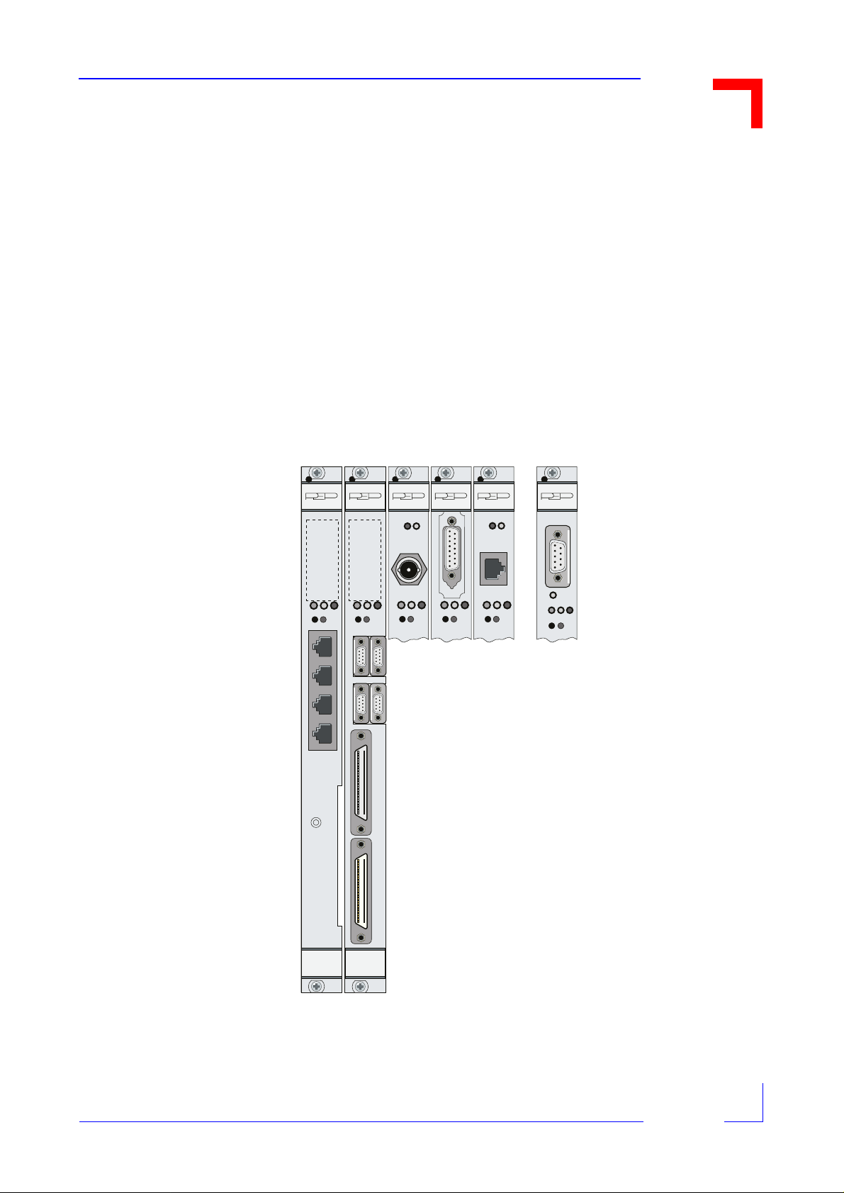
1.4 Front Panel and I/O Configuration
The illustrated front-panels show the possible connections of the SCC1 communications channel for
Ethernet, RS485 or blank. In addition, the front panels are available with mini-D-Sub connectors instead
of RJ45 connectors for the 4 standard serial channels.
The 50-pin, subminiature SCSI 2 style D-Sub connectors for emerging IP signals offer improved EMI
protection (compared with the on-board flat cable connector.) Each IP module has its o wn shielded connector for state-of-the-art industrial cabling.
All front-panels feature a user, watch-dog and halt status LED, reset and abort button switches and
where possible, the status of the Ethernet communication.
Page 1- 4
© PEP Modular Computers
Juli 23, 1997
Page 15
VM162/VM172Chapter 1 Introduction
SC and SI6 piggybacks adapt the multi-protocol serial channels of the ‘QUICC’ to the physical interfaces provided on the VM162/172’s front-panel and CXC:
SCC1 channel supports:
SI6-10B5 Ethernet 10base5 (AUI)
SI6-10B2 Ethernet 10base2 (Thin)
SI6-10BT Ethernet 10baseT (Twisted Pair)
SI6-PB485-ISO Optoisolated RS485
SCC2 to SCC4 channels support:
SC-232I Optoisolated RS232 Modem module
SC-485I Optoisolated RS485 piggyback
Figure 1.1 Front Panel Options
Ethernet,RS485 or
Blank Front-Panel
Connector
UWH
RST AB
TERM
SER1
SER2
SER3
UWH
RST AB
TERM SER 1
A
IndustryPack Interface
Ethernet,RS485 or
Blank Front-Panel
Connector
SER 3SER 2
Col Tx
10Base2
ETHERNET
UWH
RST AB
10Base5
ETHERNET
UWH
RST AB
Col Tx
10BaseT
ETHERNET
UWH
RST AB
RS485-ISO
Tx
UWH
RST AB
IndustryPack Interface B
VM162
VM162
Juli 23, 1997 Page 1- 5© PEP Modular Computers
Page 16
VM162/VM172 Chapter 1 Introduction
1.5 Features
CPU Options
The 68060 processor operating at 50 Mhz provides the highest performance while the 68040(V) at 33
MHz sets the standard in the Motorola CISC portfolio.
68EN360
The ‘QUICC’ chip operates as an I/O and communication companion providing 4, high-speed serial
channels, timers, clocks and Time Slot Assignment (TSA).
Serial Channels
All high-speed SCC channels are equipped with hardware hand-shaking and are available for a variety
of applications. SCC1 can be configured for either ethernet or RS485 (e.g. PROFIBUS) use by fitting
the appropriate SI6 piggyback. SCC2 - SCC4 are configured by default for RS232 operation and can be
changed to optoisolated RS232/485 as required by fitting the SC piggyback.An SMC1 interface provides a simple RS232 connection for console/debug operations.
Figure 1.2 MC68EN360 Channel Assignment
MC68EN360 Channel
Assignment
SCC1
MC68EN360
SMC1
SCC2 SCC3 SCC4
}
3x Serial Interfaces for
SC-Piggyback And CXC
CXC Interface
}
SI-Interface
RS232 with
Rx and Tx only
SI-Piggyback
Interface
Real-Time
Clock
SC-Piggyback
Interfaces
Page 1- 6
CXC Interface
The 96-pin interface allows other I/O possibilities to be realised by utilising PEP’ s plug-in cards such as
the CXM-PFB12, CXM-CAN, CXM-LON, CXM-SCSI or CXM-SIO3..
Ethernet Interface
Three different SI6 piggybacks complete with all the associated control logic are available providing
10Base2, 10Base5 or 10BaseT interfaces.
RS485 Interfaces
This is a fully optoisolated RS485 SI6-interfacepiggyback with a 9-pin D-Sub connector.
© PEP Modular Computers
Juli 23, 1997
Page 17

VM162/VM172Chapter 1 Introduction
IndustryPack
Any two IndustryPacks from a wide-range may be fitted to cater for the needs of digital, analog, communication or counter functions. PEP also offers customers a non-gratis service that integrates the chosen IP module and RT-OS with the VM162/172 carrier board.
SC-Interface
Three RS232 SC-Piggybacks are fitted as standard for serial communication.These can be replaced by
optoisolated RS232 or RS485 piggybacks as required.
DMA Channels
2 independent channels are provided by the ‘QUICC’ chip for use by applications requiring DMA transfer between VMEbus, CXC-modules, DRAM,FLASH memory and dual-ported SRAM.
DRAM/FLASH
This memory, complete with a 32 bit-wide access bus is placed on a piggyback with addressing capability for up to two memory banks of 64 MByte each.The on-board programmable FLASH memory allows the user to produce low cost upgrades by over-writing existing stored data and may also be
configured as a boot device.
SRAM
This is a dual-ported battery-backed (Goldcap) memory area with a 16 bit- wide access bus. Users of the
VMEbus and CPU both have access to this memory.
EEPROM
A 2 kbit EEPROM is provided on-board, 1 kbit has been pre-programmed with PEP production data leaving the remaining available space for user application code.
Juli 23, 1997 Page 1- 7© PEP Modular Computers
Page 18

VM162/VM172 Chapter 1 Introduction
1.6 Specifications
CPUs
Comms. Controller
Memory
Real-Time Clock V3021 with (year, month, week, day, hour, min., sec.)
Tick
Timer
Time-Out
Watchdog Enabled by software with front-panel LED
MC68040(V) @ 33 MHz
MC68060 @ 50 MHz
MC68EN360 Companion processor for network
support on SI6 piggybacks
1/4/16/32 MByte (32-bit access) DRAM
0.5/1/2/4 MByte (32-bit access) FLASH (Available
on DM6xx Memory Piggyback)
256 kByte or 1 MByte dual-ported SRAM with data
retention via Goldcap
2 kbit serial EEPROM for configuration data
2 ROM sockets for up to 1 MByte device (optional)
Built-in on MC68EN360 providing a programmable
periodic interrupt (default 10ms)
4x16, 2x32-bit resolution built-in timers on the
MC68EN360
On-board BERR* time-out min. 8 µ s, max.128 µ s
128 µ s VMEbus BERR* both with software enable/
disable
Interrupts
System V ectors
System Controller
Address Modifier
Slave Functions
IndustryPack Interface
CXC Interface DIN 41612 (C), 96-pin, 3 NMSI ports, DMA
VME IRQ1* - IRQ7* interrupts, enable/disable;
Mask Register; SYSFAIL* and ACFAIL* handlers
Abort switch level 7 autovector
ACFAIL* level 7 autovector
TICK level 6 vector prog.
SYSFAIL* level 5 autovector
Mailbox IRQ level 3 autovector
CXC vector prog.
Single-level (BR3*), FAIR, RWD (Release When
Done); Automatic First-Slot Detection
A32 Access Code : HEX 09/0A/0D/0E
A24 Access Code : HEX 39/3A/3D/3E
A16 Access Code : HEX 29/2D
User Defined : HEX 10-17/18-1F
Dual-ported SRAM;
16 software selectable base addresses
Two card holders with I/O ported to 50-pin flat-band
cable or D-Sub connector on front-panel
Page 1- 8
© PEP Modular Computers
Juli 23, 1997
Page 19

VMEbus Interface
DIN 41612 (C), 96-pin P1/P2 connector
A32/A24/A16:D32/D16/D8 master
A24:D16 slave
VM162/VM172Chapter 1 Introduction
Networking
SC-Interface
Power Consumption
Temperature
Humidity 0 to 95% non-condensing
Weight/Dimensions
Front Panel Functions
a. With 4 Mbyte DRAM, 256 kByte SRAM and 1 MByte FLASH memory.
a
All Ethernet interfaces conform to IEEE 802-3 and
are available on SI6-xx piggybacks
Serial Interface from MC68EN360 (ports SCC2,
SCC3 and SCC4) with standard RS232 configuration
VM162 w/ MC68060 ≈ 6.5W @ 50 MHz
VM172 w/ MC68040 ≈ 8.5W @ 33 MHz
0ºC to +70ºC (standard)
-40ºC to +85ºC (extended / storage)
440 g (with 10BaseT and memory piggybacks)
233mm x 160mm 6U format
3 LEDs: red : Halt
yellow : Watchdog enabled
green : General purpose user
Juli 23, 1997 Page 1- 9© PEP Modular Computers
Page 20

VM162/VM172 Chapter 1 Introduction
1.7 Ordering Information
Product Description Order Nr.
VMEbus single-board computer comprising MC68060 @ 50MHz,
MC68EN360 @ 25 MHz,256 kByte dual-ported SRAM (with
VM172-BASE
VM172-BASE Same as order no. 16134 but with 1 MByte dual-ported SRAM 16194
Goldcap for back-up), five serial interfaces (four available on the
front panel as RS232 (RJ45) and one available from the choice of
SI6-networking piggybacks), CXC interface, two IP interfaces and
PEPbug
16134
VMEbus single-board computer comprising MC68040 @ 33MHz,
MC68EN360 @ 33 MHz,256 kByte dual-ported SRAM (with
VM162-BASE
VM162-BASE Same as order no. 16026 but with 1 MByte dual-ported SRAM 16193
DM 600
DM 600
DM 601
DM 601
DM 602
DM 603
Goldcap for back-up), five serial interfaces (four available on the
front panel as RS232 (RJ45) and one available from the choice of
SI6-networking piggybacks), CXC interface, two IP interfaces and
PEPbug
Memory Piggyback with 4 MByte DRAM and 1 MByte FLASH
memory for VM162/172
Memory Piggyback with 4 MByte DRAM and 4 MByte FLASH
memory for VM162/172
Memory Piggyback with 16 MByte DRAM and 1 MByte FLASH
memory for VM162/172
Memory Piggyback with 16 MByte DRAM and 4 MByte FLASH
memory for VM162/172
Memory Piggyback with 1 MByte DRAM and 1 MByte FLASH
memory for the VM162/172
Memory Piggyback with 32 MByte DRAM and 512 kByte FLASH
memory for the VM162/172
16026
11852
11853
11854
11855
12765
13027
DM 603
DM 604
DM 604
SI6-10B2-IP
SI6-10B5-IP
Page 1- 10
Memory Piggyback with 32 MByte DRAM and 2 MByte FLASH
memory for the VM162/172
Memory Piggyback with 8 MByte DRAM and 1 MByte FLASH
memory for the VM162/172
Memory Piggyback with 8 MByte DRAM and 4 MByte FLASH
memory for the VM162/172
10Base2 Thin Ethernet interface piggyback with RG58 coax.
connector
10Base5 Ethernet (AUI) interface piggyback with 15-pin D-Sub
connector
© PEP Modular Computers
13627
15911
15912
16136
16137
Juli 23, 1997
Page 21

VM162/VM172Chapter 1 Introduction
Product Description Order Nr.
SI6-10BT-IP
SI6DUMMY-IP
SI6-PB485-IP
SC-2321
SC-4851
CABLE-RS232
Important : The VM162 and VM172 must be ordered with a memory module (DM60x) and a front-panel with integrated SI6-piggyback module.
For configurations requiring the 2 x 50-pin D-Sub front-panel connectors instead of the flat-band cable
option, please contact the nearest PEP sales office for further information.
10BaseT Twisted pair Ethernet interface piggyback with RJ45
connector
Front panel without networking interface(s)
Optoisolated RS485 interface piggyback with 9-Pin D-Sub
connector
Optoisolated RS232 interface piggyback with TxD, RxD, DTR and
CTS signals and Baud rate up to 38.4 kBaud
Optoisolated RS485 interface piggyback for half-duplex
communication at a Baud rate up to 38.4 kBaud
3 meter RS232 Serial Interface cable with RJ45 to 9-Pin D-Sub
(male) for terminal connection
16147
16028
16192
12919
13468
15191
1.8 Related Publications
• VMEbus Specifications VME64
• IndustryPack
• CXC Specification from PEP (Version 1.5 or later)
Juli 23, 1997 Page 1- 11© PEP Modular Computers
Page 22
VM162/VM172 Chapter 1 Introduction
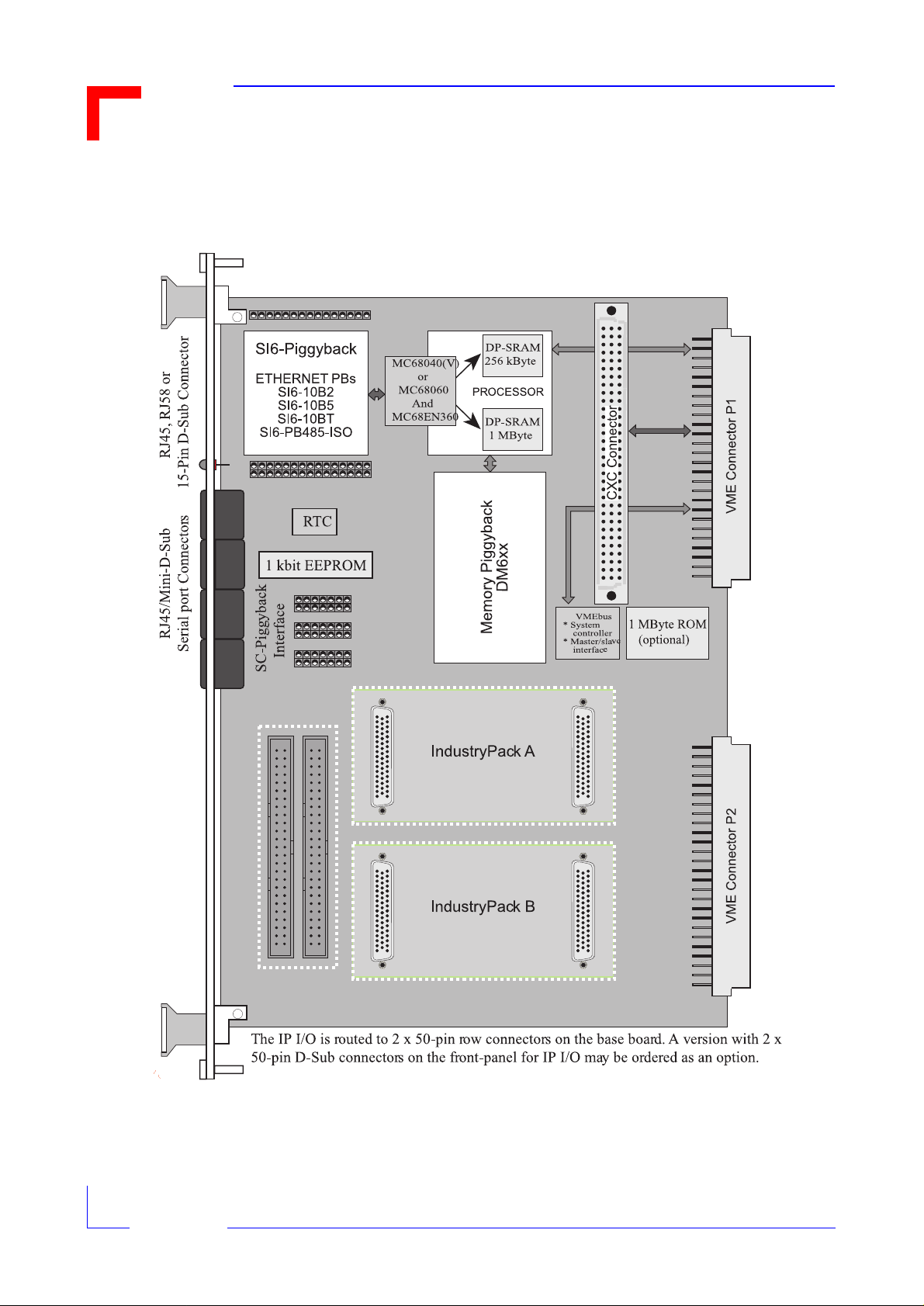
1.9 Schematic Board Layout
Page 1- 12
© PEP Modular Computers
Juli 23, 1997
Page 23

VM162/VM172
Functional Description
2.1 VM162/VM172 Block Diagram.....................................................2-3
2.2 CPU Options.................................................................................2-4
2.3 Memory..........................................................................................2-4
2.3.1 DRAM/FLASH...............................................................................................2-4
2.3.2 SRAM.............................................................................................................2-5
2.3.3 Boot ROM (optional).....................................................................................2-5
2.3.4 EEPROM.......................................................................................................2-6
2.4 Communication Controller 68EN360 (QUICC)...........................2-6
2.4.1 Use of 68EN360 Communication Ports........................................................2-6
2.4.2 Use of 68EN360 Memory Controller............................................................2-7
2.4.3 Use of 68EN360 Interrupt Controller...........................................................2-7
2.4.4 Use of 68EN360 DMA Channels...................................................................2-8
2.5 VMEbus Interface..........................................................................2-8
2.5.1 VME Master Interface...................................................................................2-9
2.5.2 System Controller Functions.......................................................................2-10
2.5.3 VME Slave Interface ...................................................................................2-11
2.5.4 VME Address Map from the VME Side.......................................................2-12
2.5.5 VME Control/Status Register......................................................................2-13
2.6 Board Control Logic ...................................................................2-14
2.6.1 Boot Decoder Logic ....................................................................................2-14
2.6.2 Interrupt Control.........................................................................................2-14
2.6.3 Bus Timer....................................................................................................2-16
2.6.4 Watchdog Timer..........................................................................................2-16
2.6.5 Board Control/Status Register....................................................................2-16
2.7 Special Functions........................................................................2-18
2.7.1 Real Time Clock..........................................................................................2-18
2.7.2 Serial EEPROM..........................................................................................2-18
2.7.3 TICK Timer .................................................................................................2-18
2.7.4 General Purpose Timer...............................................................................2-18
2.7.5 DMA Transfers............................................................................................2-18
2.7.6 Data Retention for RTC and SRAM............................................................2-19
2.7.7 Front Panel Buttons and LED Ports...........................................................2-19
2.8 Serial Communication Ports.......................................................2-20
2.8.1 Ethernet/SER4 Port.....................................................................................2-21
2.8.2 SER1, SER2 and SER3 Ports ......................................................................2-22
Chapter
2
Juli 23, 1997 Page 2- 1© PEP Modular Computers
Page 24

VM162/VM172 Chapter 2 Functional Description
2.8.3 TERM Pinouts............................................................................................. 2-23
2.9 CXC Interface .............................................................................2-24
2.10 IndustryPack (IP) Interface ...................................................... 2-30
2.10.1 Overview...................................................................................................2-30
2.10.2 Features.................................................................................................... 2-30
2.10.3 Optional IP features, not supported .........................................................2-30
2.10.4 IP Interface Controller .............................................................................2-31
2.10.5 IP Reset Control........................................................................................2-31
2.10.6 IP Clock Control.......................................................................................2-31
2.10.7 IP Interrupt Control.................................................................................. 2-31
2.10.8 IP Memory Size Control ...........................................................................2-32
2.10.9 IP Interface Address Map.........................................................................2-32
2.10.10 Interrupt Control Register...................................................................... 2-33
2.10.11 Slot Control Register ..............................................................................2-34
2.10.12 Connectors..............................................................................................2-35
Page 2- 2
© PEP Modular Computers
Juli 23, 1997
Page 25
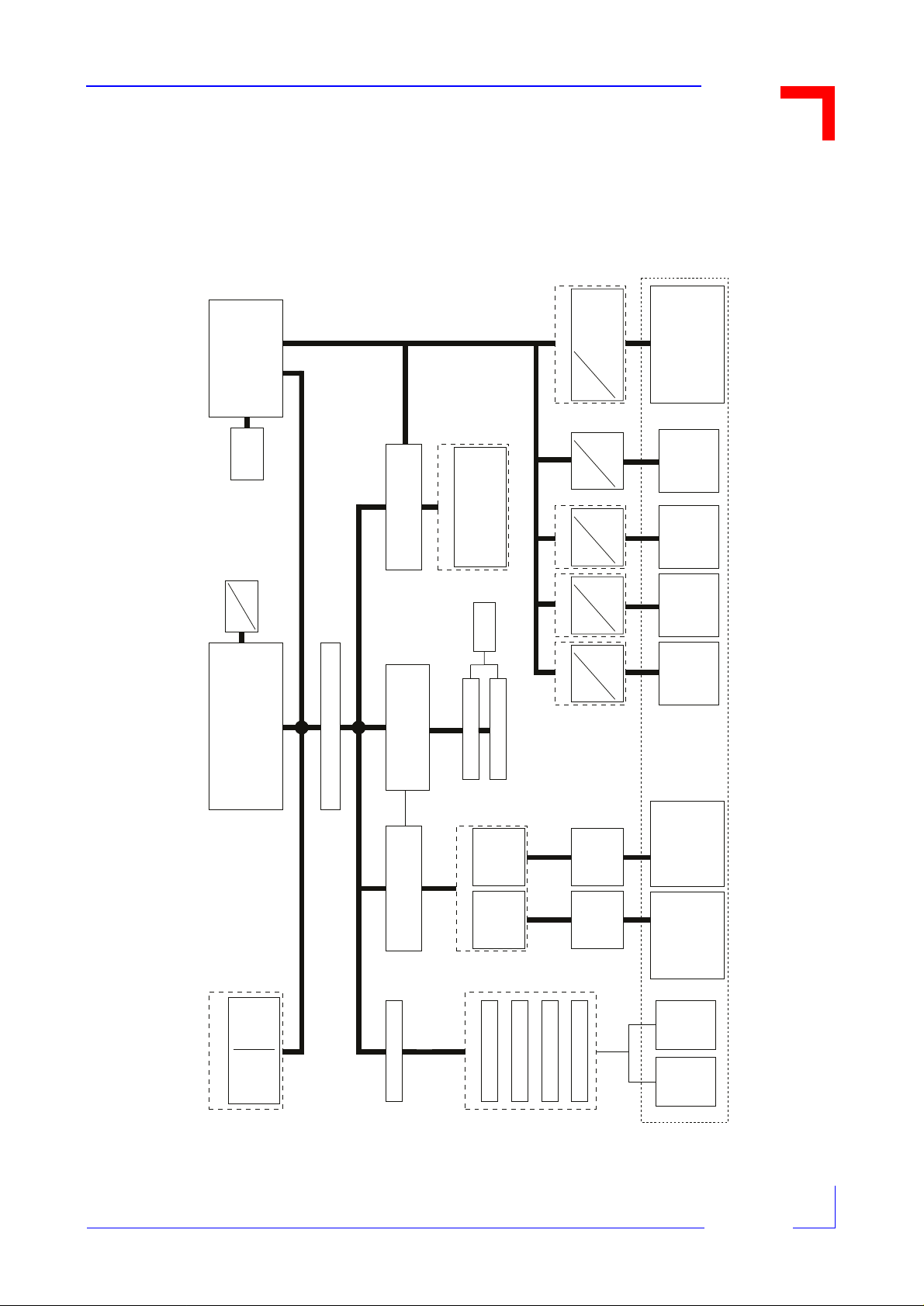
2.1 VM162/VM172 Block Diagram
68EN360
25/33 MHz
I/O Processor
SI-PB
10Base5
10Base2
TTL
RS485 Iso
10BaseT
VM162/VM172Chapter 2 Functional Description
or
or
or
(10BT)
(RS485 iso.)
(AUI)
(10B2)
(SER4)
Ethernet/Fieldbus
RG58
DSUB-15
RJ45
DSUB-9
3.3 V
CPU
serial
EEPROM
5V
33 MHz
50/66 MHz
68060
68040
Enhanced
CXC Interface
VME Interface
Bussizer/Buffers
Master: A32/D32
Slave: A24/D16
I/O
I/O
I/O
(DMA)
CXM (opt.)
Digital
Analog
SCSI
Serial
Backup
DualPortSRAM
etc.
Controler
RealTimeClock
B
IP Slot
SC-PB
SC-PB
SC-PB
TTL
TTL
TTL
TTL
IP - I/O
RS232
RS485
RS232
(opt.Iso)
RS485
RS232
(opt.Iso)
RS485
RS232
(opt.Iso)
Conn.
FlatCable
Ser I/O
Ser I/O
Ser I/O
Ser I/O
IP - I/O
(TERM)
(SER1)
(SER2)
(SER3)
MDSUB-9
RJ45 or
MDSUB-9
RJ45 or
MDSUB-9
RJ45 or
RJ45 or
MDSUB-9
FrontPanel
DSUB-50 Conn.
IP Slots
A
IP Slot
Register
Board
BoardControlLogic
Timer
Handler
Bus
IRQ
FLASH
0-4 MB
Memory-PB
1-64 MB
DRAM
Interface
Industry Pack
BootROM (opt.)
Juli 23, 1997 Page 2- 3© PEP Modular Computers
Conn.
FlatCable
IP - I/O
Timer
Watchdog
IP - I/O
Port
LED
ABORT
RESET/
DSUB-50 Conn.
Buttons
Page 26

VM162/VM172 Chapter 2 Functional Description
2.2 CPU Options
By supporting several types of CPUs the VM162/VM172 pro vides scalable computing po wer at optimized costs.
The CPU types differ in performance, power requirement and supported functions. Optional on-chip
functions are Memory Management Unit (MMU) and Floating Point Unit (FPU).
There are three categories of VM162/VM172 CPU boards. At the top there is the 68060 CPU board
which offers 2 to 3 times performance of a the following 68040 CPU board. At the low end there is the
CPU 68040V board which is the low cost and also low power version.
The Table below summerizes the differences between the CPU versions:
Table 2.1: CPU Options
CPU Type
68060 50 yes yes 133779 18.28 high performance
68040 33 yes yes 61255 9.43 standard
68040V 33 yes no 61255 - lower cost/low power
68060 66 yes yes TBD TBD planned
Note: Performance data based on the same test for all CPU versions of the VM162/VM172 is intended
to demonstrate the performance ratio between them.
The above measurements have been made under the OS-9 operating system version 3.0 with the UltraC compiler version 1.3.1.
2.3 Memory
Freq
MHz
MMU FPU
Integer
Performance
(
Dhrystone
Floating Point
Performance
(
)
Wheatstone
)
2.3.1 DRAM/FLASH
DRAM and FLASH memory is combined on a piggyback with addressing capabiltity for up to 64 MBytes each. It provides a fast 32 bit data access with DRAM Burst support. It provides also in-system
FLASH programming facility, thus ROM upgrades are easy and cost-effective by simply overwriting
existing stored data in FLASH. Hardwired write protection of FLASH can be optionally selected by
jumper.
The Table on the following page summarizes the variety of DRAM/FLASH modules present available
(refer also to the Memory Piggybacks Appendix). Please consult your sales representati v e for other possible applications.
Page 2- 4
© PEP Modular Computers
Juli 23, 1997
Page 27

VM162/VM172Chapter 2 Functional Description
Table 2.2: DRAM/FLASH Options
Name DRAM Size FLASH Size
DM600 4 MByte 1 or 4 MByte
DM601 16 MByte 1 or 4 MByte
DM602 1 MByte 0 or 0.5 or 2 MByte
DM603 32 MByte 1 or 4 MByte
DM604 8 MBytes 1 or 4 MBytes
Note: DRAM is accessed with a 5-2-2-2 burst cycle at 25 MHz bus clock (68060/50MHz) and with a 62-2-2 burst cycle at 33 MHz bus clock (68040(V)/33MHz).
2.3.2 SRAM
The SRAM on the VM162/VM172 is or ganized in one bank with 16 bit wide data access b us. It is bakked by two onboard service-free GoldCaps and optionally via VME StandBy. Additionally, this memory is dual-ported. Users of the VMEbus and the onboard CPU both have access to this memory.
The dual-ported SRAM is soldered directly on the base board available with size of 256 kB or 1 MB.
2.3.3 Boot ROM (optional)
The VM162/VM172 Boot R OM is an optional sock et de vice. The sockets support de vices up to 512 kB
size with a 16 bit wide data access for PLCC EPROMs.
By default, the board’s firmw are is stored directly in the FLASH on memory piggyback. Thus, the Boot
ROM is not mandatory. In case of using a Memory-PB without FLASH or if an application requires the
board’s firmware to be separated from FLASH then the Boot R OM sock et can be used. Whether starting
from FLASH or from Boot ROM is selected by jumper.
Supported chips for the Boot ROM:
128Kx8, 256Kx8, 512Kx8 PROM or EPROM, Standard JEDEC Pinning
Juli 23, 1997 Page 2- 5© PEP Modular Computers
Page 28

VM162/VM172 Chapter 2 Functional Description
2.3.4 EEPROM
The EEPROM is a non-volatile serial memory device. It provides 2 kbit size and is accessed over the
SPI (Serial Peripheral Interface) of the 68EN360.
1 kbit of this EEPROM memory is free for application relevant data whereas the rest of this EEPROM
is reserved. This part is used for storing board ID codes, Internet/Ethernet addresses and boot information.
Note: For more information on the EPROM type, please refer to the XICOR X25C02 data sheet. For
EEPROM internal address mapping, also refer to the Programming Chapter in this manual.
2.4 Communication Controller 68EN360 (QUICC)
The 68EN360 QUICC (Quad IntegratedCommunication Controller), serves as an I/O controller/processor on the VM162/VM172. This device is especially optimized for serial communication.
Therefore, it provides an unique internal hardware architecture and supports a variety of communication
protocolls and operating modes.
In addition, the QUICC is used for some on-board system functions such as DRAM control, Tick generation and address decoding by operating in the so-called companion mode. In this mode its own CPU32
core is disabled whereas all other features including its Communication Processor Module (CPM) are
still available.
In terms of communication tasks the QUICC works as a co-processor to the CPU. Its internal communication „hardware“ is built up with a command programmable Communication Processor , 14 dedicated
DMA channels, 4 Serial Communication Controllers (SCC), 2 Serial Management Controllers (SMC)
and a Time-Slot Assigner (TSA).
Among many others, protocolls supported by the SCCs for example are UART, HDLC/SDLC, Apple
Talk, Ethernet/IEEE 802.3, X.21 and Signaling System # 7. The Time-Slot Assigner supports building
2 time-domain-multiplexed (TDM) channels to be for instance E1/T1, ISDN Basic/Primary Rate or
User Defined.
Warning!
In the PEP supported BSP’s for OS-9 version 3.0, PEP makes sur e that the proper initialization sequence for the QUICC is followed. Never change this initialization sequence, as unexpected errors may occur.
2.4.1 Use of 68EN360 Communication Ports
Page 2- 6
The 68EN360 provides 5 serial ports based on 4 SCCs and 1 SMCs. These multiprotocol serial ports can
be physically translated to the different standards due to application specific demands. This translation
is very flexible on the VM162/VM172 by using SI- and SC- piggybacks or even CXMs. 5 configured
serial ports are available at front panel connectors.
© PEP Modular Computers
Juli 23, 1997
Page 29
VM162/VM172Chapter 2 Functional Description
2.4.2 Use of 68EN360 Memory Controller
Beside its main purpose which is to provide communication power to the VM162/VM172 the I/O controller 68EN360 is also used for some system integration function. First of all this is DRAM control and
global memory decoding. Therefore, the 8 CS lines provided by the 68EN360 memory controller are
connected to the different memory types or address areas folllowing the scheme in the following Table.
Table 2.3: 68EN360 CS Line Connection
68360 CS Line Connection
CS0 FLASH
CS1 DRAM
CS2 VMEbus via DMA
CS3 Reserved
CS4 SRAM
CS5 CXC
CS6 RTC
CS7 Board Register
Note: In order to be compatible with the above configuration, the board initialization described in the
Programming Chapter must be closely adhered to.
2.4.3 Use of 68EN360 Interrupt Controller
The 68EN360 internal interrupt controller is one part of the VM162/VM172 interrupt control logic. The
68360 internal interrupt controller provides programmable interrupt vectors for all internal interrupt requests. For detailled description of these interrupts, please refer to the 68EN360 User’s Manual.
Additionally, some external signals are connected with 68EN360 dedicated interrupt inputs. Signals at
this inputs are processed by the 68EN360 to generate autovectored interrupt on fixed le vels to the CPU.
These signal are summarized below:
Table 2.4: External Signal Connection
Signal
ABORT/ACFAIL 7
Generated
Autovector
Mailbox 5
SYSFAIL 3
Reserved 2
Reserved 1
Juli 23, 1997 Page 2- 7© PEP Modular Computers
Page 30

VM162/VM172 Chapter 2 Functional Description
Note: In order to be compatible with the above configuration, the board initialization described in the
Programming Chapter must be closely adhered to.
VME ACFAIL* generates a non-maskable autovector level 7 interrupt (NMI) in the same way as the AB-
ORT button. When an ACFAIL* NMI is detected, it can be differentiated fr om an ABORT by reading bit
1 of the Board Configuration Register.
2.4.4 Use of 68EN360 DMA Channels
The 68EN360 includes altogether 14 DMA channels which are dedicated to the communication ports
(SDMA) and 2 independant DMA channels (IDMA). With the IDMAs memory to memory transfers
are possible with any combination of onboard and A24/D16 VME addresses.
Note: In order to be compatible with CPU VME and DMA VME transfers, the board initialization described in the Programming Chapter must be closely adhered to.
2.5 VMEbus Interface
The VM162/VM172 has a complete VMEbus Master interface with arbiter, system clock driver, power
monitor with system reset driver, IACK daisy chain driver and a 7-level VMEbus interrupt handler.
The VM162/VM172 VMEbus Master interface supports A32, A24 and A16 addressing modes in any
combination with D32, D16 and D8 data bus width.
Arbitration is single level FAIR on BR3. Used as system controller the board has to be placed in slot 1
of the VMEbus backplane (furthermost left slot).
VMEbus system signals ACFAIL* and SYSFAIL* are processed by the VM162/VM172 to autovectored interrupt requests (see also the Use of 68EN360 Interrupt Controller Section).
In addition, the board provides also a VMEbus Slave interface which consists of a dual-ported RAM
with programmable board address and a mailbox interrupt facility.
Page 2- 8
© PEP Modular Computers
Juli 23, 1997
Page 31

VM162/VM172Chapter 2 Functional Description
2.5.1 VME Master Interface
2.5.1.1 Supported Data Transfer Types (VMEbus AM Codes)
The VM162/VM172 supports three addressing modes which are A32, A24 and A16. The following AM
codes according to the standard for VME64 are supported by the VM162/VM172.
Table 2.5: External Signal Connection
AM Code (Hex) Function
3E A24 supervisory program access
3D A24 supervisory data access
3A A24 non-privaleged program access
39 A24 non-privaleged sata access
2D A16 supervisory access
29 A16 non-privaleged access
1F - 18 User Defined
17 - 10 User Defined
0E A32 supervisory program access
0D A32 supervisory data access
0A A32 non-privileged program access
09 A32 non-privileged data access
Note: For the user-defined codes 1F - 18 and 17 - 10, there are A24/D16 cycles generated by the
VM162/VM172.
Juli 23, 1997 Page 2- 9© PEP Modular Computers
Page 32

VM162/VM172 Chapter 2 Functional Description
2.5.1.2 VME Address Map
The various combinations of addressing modes and data bus sizes are selected on dif ferent address areas
within the address map of the CPU. The corresponding AM codes are generated according to the T able
below.
Table 2.6: Generated AM Codes
VME
AM Code
0E/0D/0A/09 A32/D32 512 MByte 00 00 00 00 - 1F FF FF FF A0 00 00 00 - BF FF FF FF
0E/0D/0A/09 A32/D16 256 MByte 00 00 00 00 - 0F FF FF FF 90 00 00 00 - 9F FF FF FF
3E/3D/3A/39 A24/D32 16 MByte xx 00 00 00 - xx FF FF FF 8F 00 00 00 - 8F FF FF FF
3E/3D/3A/39 A24/D16 16 MByte xx 00 00 00 - xx FF FF FF 87 00 00 00 - 87 FF FF FF
2D/29 A16/D32 64 kByte xx xx 00 00 - xx xx FF FF 8D 00 00 00 - 8D 00 FF FF
2D/29 A16/D16 64 kByte xx xx 00 00 - xx xx FF FF 85 00 00 00 - 85 00 FF FF
VME
Cycle T ype
Size
(HEX)
VME Address Range
(HEX)
CPU Address Range
(HEX)
Note: The A32 VME addressing modes begin at VME offset 0, independent of their location within the
CPU address map.
Supervisor/use or program/data AM codes are generated, dependent on the type of CPU access that is
running.
2.5.2 System Controller Functions
2.5.2.1 Automatic First-Slot Detection
During power-up, the VM162/VM172 automatically detects if the board is placed in the far left slot of
the system. If so, it acts automatically as the system controller.
Note: This information is stored in the FSD (First Slot Detection) bit within the VMEbus Control/Status
register .
2.5.2.2 SYSCLK* Generator
The VMEb us SYSCLK* driver of the VM162/VM172 is controlled directly by the FSD bit. That means,
if the board has detected itself as system controller it will automatically drive SYSCLK* to the VMEbus. If it has detected not to be system controller its SYSCLK* driver is automatically disabled.
Note: The system integrator has to ensure that there is only one SYSCLK driver active for the whole system. This is especially important where boards with jumper enabled SYSCLK drivers are mixed with
VM162/VM172 boards.
Page 2- 10
© PEP Modular Computers
Juli 23, 1997
Page 33

VM162/VM172Chapter 2 Functional Description
2.5.2.3 SYSRES* Generator
The VM162/VM172 contains a power monitor which generates on-board system reset signal after the
on-board voltage falls below 4.65 V. This on-board system reset can also drive VME SYSRES*. If the
VM162/VM172 is not intended to drive VME SYSRES*, the signal can be disconnected using a jumper .
Note: In contrast to SYSCLK*, which may be driven by one board in the system, SYSRES* may be
driven more than once in a system.
SYSRES* originating from another power monitor within the system always resets the VM162/VM172.
2.5.2.4 VMEbus Monitor
The VM162/VM172 also provides a bus monitor for the VMEbus. A 128 µs timeout timer monitors
VMEbus data transfer cycle lengths and generates a VMEb us BERR* signal for error termination. This
timer is enabled/disabled via the VME Control/Status Register, which also supplies a timeout status bit
in order to identify bus errors generated by the VMEbus monitor.
2.5.3 VME Slave Interface
2.5.3.1 Dual-Ported RAM
The VM162/VM172 provides 256 kByte or 1 MByte of on-board SRAM which is dual-ported between
the CPU and VMEb us. Read-Modify-Write cycles (TAS instruction used for semaphores) are supported
in any direction.
The location of the dual ported SRAM as seen from VME is programmable via the VME Control/Status
Register. There are 16 different base addresses possible with separate enable/disable functions all located in VME A23/D16 space.
Note: The lowest 8 kByte of the dual-ported SRAM is reserved for generating mailbox interrupts.
2.5.3.2 Mailbox Interrupt
An external VMEb us master may interrupt the VM162/VM172 by setting the corresponding mailbox interrupt bit. This bit called P_IRQ5 is placed within the VME Control/Status Register. Setting this bit generates an autovectored 5 interrupt on the CPU. Typically, the on-board CPU resets P_IRQ5 during
processing the corresponding interrupt service routine.
Notes:
The complete VME Control/Status Register can be read also from an external VMEbus Master. It is
addressed on every odd addr ess of the lowest 8 kByte block of the VME board addr ess. Only the mailbox
interrupt P_IRQ5 can, however, be set; all other bits are write protected from the VME.
As the P_IRQ5 bit is located at bit 7 of the register, it can be directly used as a semaphore due to the fact
that Read-Modify-Write access is supported.
Although the VM162/VM172 cannot access itself via the VMEbus, setting the mailbox interrupt bit on
the local side also generates the interrupt to the CPU.
Juli 23, 1997 Page 2- 11© PEP Modular Computers
Page 34

VM162/VM172 Chapter 2 Functional Description
2.5.4 VME Address Map from the VME Side
The T able belo w shows the VME board address map for external Master access dependent on the setting
of the board address bits within the VME Control/Status Register.
Table 2.7: VME Address Map
Board
Address
Bits
BADR[3-0]
0 00 00 00 00 00 00 - 00 1F FF 00 20 00 - 0F FF FF
1 10 00 00 10 00 00 - 10 1F FF 10 20 00 - 1F FF FF
2 20 00 00 20 00 00 - 20 1F FF 20 20 00 - 2F FF FF
3 30 00 00 30 00 00 - 30 1F FF 30 20 00 - 3F FF FF
4 40 00 00 40 00 00 - 40 1F FF 40 20 00 - 4F FF FF
5 50 00 00 50 00 00 - 50 1F FF 50 20 00 - 5F FF FF
6 60 00 00 60 00 00 - 60 1F FF 60 20 00 - 6F FF FF
7 70 00 00 70 00 00 - 70 1F FF 70 20 00 - 7F FF FF
8 80 00 00 80 00 00 - 80 1F FF 80 20 00 - 8F FF FF
9 90 00 00 90 00 00 - 90 1F FF 90 20 00 - 9F FF FF
A A0 00 00 A0 00 00 - A0 1F FF A0 20 00 - AF FF FF
B B0 00 00 B0 00 00 - B0 1F FF B0 20 00 - BF FF FF
C C0 00 00 C0 00 00 - C0 1F FF C0 20 00 - CF FF FF
Board VME Base
Address (HEX)
Mailbox Interrupt Reg.
Address Range
(HEX)
Dual-ported SRAM
Address Range
(HEX)
D D0 00 00 D0 00 00 - D0 1F FF D0 20 00 - DF FF FF
E E0 00 00 E0 00 00 - E0 1F FF E0 20 00 - EF FF FF
F F0 00 00 F0 00 00 - F0 1F FF F0 20 00 - FF FF FF
Note: All of the possible board address ranges are located in VME A24/D16 addressing mode. It is enabled for supervisor/user data access in accordance to AM codes 3D and 39.
Page 2- 12
© PEP Modular Computers
Juli 23, 1997
Page 35

VM162/VM172Chapter 2 Functional Description
2.5.5 VME Control/Status Register
The VME Control/Status Register is a one byte wide register with read/write access at default address
CD 00 00 05 (HEX).
01234567
CS7 + $5
P_IRQ5 FSDEN_BERR2EN_DPR
Note: All bits except bit 4 (First Slot Detection) are clear ed after r eset. The firmware of the board initializes some of them at startup according to the default parameters stored in the EEPROM.
Register Description
Name Value
P_IRQ5
bit 7
EN_DPR
bit 6
EN_BERR2
bit 5
FSD
bit 4
1
1
1
1
Reset (HW)
Slot 1 Other
00
00
00
10
Reset PEP (SW)
Slot 1 Other
00
Value stored in
EEPROM
10
10
BADR2BADR3 BADR1 BADR0
Description
Pending mailbox IRQ
Dual-port RAM (inc. mailbox IRQ) for
VME requester enabled. Base address
fixed using BADRx bits
Enable bus monitor timer, all VME
cycles, timeout after 128µs
VMEbus ‘First Slot Detection’ flag,
system controller
BADR3 BADR0
bits 3-0
00
Value stored in
EEPROM
VME address location of dual-ported
RAM. Equivalent to VME address lines
A23-A20, programmable from $0-$F in
1 MByte windows, enabled with
EN_DPR
Note: All bits are cleared during a reset. FSD is set dependent on the slot position of the board in the
system. The board’s firmware initializes EN_DTR, EN_BERR2 and BADR[3-0] during startup following default parameters stored in the serial EEPROM.
Juli 23, 1997 Page 2- 13© PEP Modular Computers
Page 36

VM162/VM172 Chapter 2 Functional Description
2.6 Board Control Logic
2.6.1 Boot Decoder Logic
The VM162/VM172 gives the user the choice to execute startup procedures from three different memory areas. These are FLASH (default on the memory Piggyback), or the optional Boot ROM or memory on the VMEbus. The boot device/memory is selected by jumpers.
The boot decoder logic redirects the initial CPU access which is always starting at address 0 (HEX) to
the boot device according the boot jumper setting. The boot device is swiched automatically to its default address area after the first access on it with its default address.
For more details, please refer to the Programming Chapter in this manual.
Notes: If VMEbus memory is selected to be the default boot device, it must be located at VME base
address 0 (HEX) in A24/D16 address space for supervisory program/data access (AM codes 3E, 3D).
If FLASH or VMEbus memory is selected to be the boot device, the optional Boot ROM can be used as
a standard ROM for storing program, data or application specific parameters.
2.6.2 Interrupt Control
The interrupt control logic processes internal interrupt requests (68EN360), together with external requests (VME) and external autovectored interrupt requests. The interrupt control logic is built up using
the 68EN360 internal interrupt controller for QUICC internal 68EN360 and a seven level VMEbus interrupt handler with the corresponding mask register.
2.6.2.1 Internal Requests
Internal requests are related to all interrupt requests caused by the 68EN360 sources, including the
68EN360 system integration functions (watchdog timer, periodic interrupt timer) and the communication processor module (RISC controller, timers, DMAs, SCCs and so on). For more information, please
refer to the 68EN360 User’s Manual.
In order to avoid conflicts regarding interrupt le vels, it is recommended to use IRQ le v el 4 for 68EN360
CPU internal requests and IRQ level 6 for 68EN360 SIM60 internal requests.
Note: The four IRQ lines specified by CXC are supplied by the 68EN360 Port C lines and ar e, therefor e,
also processed as internal requests (PC0, 1, 2, 3).
Page 2- 14
© PEP Modular Computers
Juli 23, 1997
Page 37

VM162/VM172Chapter 2 Functional Description
2.6.2.2 External Autovectored Interrupt Requests
Autovectored interrupts are all generated via the 68EN360 pins for external interrupt sources. The y are
summarized in the table below . Care must be taken that the rele v ant 68EN360 register is initialised with
respect to the wiring (see also the Programming chapter in this manual).
Table 2.8: External Autovectored Interrupts
Source 68EN360 Pin Autovector
ABORT/ACFAIL IRQ7 7
TICK IRQ6 6
Mailbox IRQ IRQ5 5
SYSFAIL IRQ3 3
2.6.2.3 VME Interrupt Mask Register
CS7 + $1
The VME Interrupt Mask Register is a one byte wide register with read/write access situated at default
address CD 00 00 01 (HEX). All bits are cleared after reset.
01234567
EN_IRQ7 EN_IRQ4EN_IRQ5EN_IRQ6
ReservedEN_IRQ3 Reserved SYSFAIL
Note: The firmware of the board initializes this register using the default parameters stored in the EEPROM.
Register Description
Name Value Description
EN_IRQ7
EN_IRQ6
EN_IRQ5
EN_IRQ4
EN_IRQ3
EN_IRQ2
EN_IRQ1
SYSFAIL
1
1
1
1
1
1
1
1
Enable VME IRQ7
Enable VME IRQ6
Enable VME IRQ5
Enable VME IRQ4
Enable VME IRQ3
Enable VME IRQ2
Enable VME IRQ1
Enable VME SYSFAIL IRQ
Juli 23, 1997 Page 2- 15© PEP Modular Computers
Page 38

VM162/VM172 Chapter 2 Functional Description
2.6.3 Bus Timer
The VM162/VM172 provides an 128µs timeout timer which monitors the cycle lengths of on-board
data transfers, including on-board I/O, CXC, IndustryPack, dual-ported SRAM and some VME. After a
timeout occurs, it generates an on-board BERR signal for error termination.
This timer is enabled / disabled via the Board Control/Status Register, which also supplies a timeout status bit in order to identify bus errors generated by the on-board bus error timer.
Note: During VMEbus cycles, the on-board bus err or timer is r eset as soon as the VM162/VM172 gains
VMEbus ownership. This means that the time gap between a VMEbus request and the start of a VMEbus
cycle is monitored by the on-boar d Bus T imer. VMEbus cycles themselves are monitored by the separate
VME Bus Monitor.
2.6.4 Watchdog Timer
A 512ms watchdog timer is also provided by the VM162/VM172. Once enabled via the Board Control/
Status Register, the watchdog timer cannot be reset by software. It must be re-triggered via the corresponding bit in the Board Control/Status Register periodically within the timeout period.
‘Watchdog timer running’ is a status that is displayed by the yellow front panel LED. At timeout, the
watchdog timer triggers the on-board system reset.
Note: If the board’s VME SYSRES* jumper is set, the watchdog timer can reset the whole of the VME
system.
2.6.5 Board Control/Status Register
The Board Control/Status Register is a one byte wide register with read/write access at default address
CD 00 00 07 (HEX).
CS7 + $7
WDG EN_WDGBERR1BERR2
Note: Information may be lost if the user writes to bit 7.
01234567
EN_BERR1TR_WDG ACFAIL LED_G
Page 2- 16
© PEP Modular Computers
Juli 23, 1997
Page 39

Register Description
Name Value Access Description
VM162/VM172Chapter 2 Functional Description
WDG
bit 7
BERR2
bit 6
BERR1
bit 5
EN_WDG
bit 4
TR_WDG
bit 3
EN_BERR1
bit 2
ACFAIL
bit 1
LED_G
bit 0
Read/Write
Read/Write
Read/Write
1
1
1
1
1
Read/Write
Read/Write
Read/Write
Read/Write
Read/Write
Set by watchdog timer when timeout has been reached.
Used to differentiate between resets caused by the
watchdog and resets caused by the reset button (power up
resets can be identified within the 68EN360).
Set by VMEbus BUS monitor when timeout has been
reached. Used to identify BERR caused by this timer (see
also VMEbus Control/Status Register).
Set by on-board bus error timer when timeout has been
reached. Used to identify BERR caused by this timer.
Enable the watchdog timer. It can only be set once, and
remains enabled until the next reset.
Triggers the watchdog timer. Watchdog timeout=512ms.
Enables the on-board bus error timer. It also monitors all
on-board I/O cycles, including the time from the VMEbus
request to the VMEbus grant. Timeout=8µs.
VME ACFAIL signal latched when active in order to
distinguish between a level 7 NMI from an ABORT or
ACFAIL.
Enables the green ‘general purpose’ front panel LED.
Juli 23, 1997 Page 2- 17© PEP Modular Computers
Page 40

VM162/VM172 Chapter 2 Functional Description
2.7 Special Functions
2.7.1 Real Time Clock
The RTC (V3021 3-wire serial interface) is a 1-bit device which is accessible over the CS6 of the
68EN360. Its timekeeping features include:
• seconds, minutes, hours, day of month, month, year, week day and week number in BCD format.
• leap year and week number correction.
• standby supply smaller than 1µA.
For more details, please refer to the Programming Chapter in this manual and the V3021 data sheet.
2.7.2 Serial EEPROM
The serial EEPROM is a 1-bit device which is accessible o ver the SPI Interface (3-wire Interchip) of the
68EN360. The first half of the EEPROM (1 kbit) is reserv ed for factory data, including Board ID codes,
Internet/Ethernet addresses, boot information etc. The second half of the EEPROM is available for the
user. See also the Programming Chapter in this manual.
For more information on the EEPROM, please refer to the XICOR X25C02 data sheet.
2.7.3 TICK Timer
The 68EN360 internal Periodic Interrupt Timer is used by the PEP supported real-time operating systems as TICK generator.
For more information, please refer to the 68EN360 User’s Manual.
2.7.4 General Purpose Timer
There are four 16-bit general purpose timers available which are provided by the 68EN360. Two pair of
timers can cascaded internally or externally to form two 32-bit timers. Maximum period is 8.1s at
33MHz with a resolution of 30ns.
For more information please refer to the 68EN360 User’s Manual.
2.7.5 DMA Transfers
There are two independant fully programmable DMA channels available which are provided by the
68EN360. These IDMAs provide 32-bit address and 32-bit data capabiltity together with 32-bit byte
transfer counters. Fixed and rotating priority as well as single buffer, auto buffer or buffer chaining is
supported by the DMAs. With the IDMAs memory to memory transfers are possible with any combination of onboard and A23/D16 VME addresses.
For more information please refer to the 68EN360 User’s Manual.
Page 2- 18
© PEP Modular Computers
Juli 23, 1997
Page 41

VM162/VM172Chapter 2 Functional Description
2.7.6 Data Retention for RTC and SRAM
Short term data retention for RTC and SRAM is gained with tw o Gold-Caps, each with a value of 0.22
Farad. In contrast to Lithium cells, Gold-Caps do not require servicing. This short term backup is intended for short power failures or for reconfiguring systems. An empty Gold-Cap needs approximately
three hours to charge up, with backup times dependant on the temperature, memory size and memory
manufacturer tolerances. A well charged Gold-Cap provides a minimum of 10 hours backup time.
Laboratory tests at PEP indicate a typical backup time of 1 week for both 256kB and 1MByte SRAM
plus RTC (typical onboard backup current is 2 µA).
Long term data retention is made via the VMEb us 5V Stby line. W ith respect to the VM162/VM172, this
voltage can drop to 2.5V, with the typical current via the 5V Stby being 30µA at 3V.
Notes: The VM162/VM172 board can be removed from the system and plugged in again without losing any information. Data retention switches from the VME 5V Stby to the on-board Gold-Caps automatically.
The on-board Gold-Caps ar e continuously reloaded via the 5V Stby line. The 5V Stby curr ent is typically
7mA for a few minutes when the Gold-Caps are at the beginning of the loading phase (fully dischaged).
2.7.7 Front Panel Buttons and LED Ports
Figure 2.1 LED Port and Button Location
Watchdog LED
Yellow
User General Purpose
Green
W
UH
RESET Switch ABORTSwitch
RST AB
2.7.7.1 RESET/ABORT Button
A RESET button is fitted to the front panel to avoid f alse operation. The RESET button triggers the onboard system reset generator, as well as the VME if jumper J2 is set.
T ogether with the RESET b utton, an ABORT button is also fitted to the front panel. The ABORT button
generates a level 7 IRQ (non-maskable interrupt) which is used for debugging purposes. In this case, bit
1 of the Board Control/Status Register is not set (remains ‘0’).
2.7.7.2 LED Port
The front panel LED port consists of three LEDs with the following functions:
CPU HALTor RESET
Red
Red LED CPU in HALT or RESET status.
Yellow LED Watchdog timer running status.
Green LED General purpose, set via Board Control/Status Register.
The green LED is free to be used by the customer. It is set by the software during startup when the
68EN360 is initialized.
Juli 23, 1997 Page 2- 19© PEP Modular Computers
Page 42

VM162/VM172 Chapter 2 Functional Description
2.8 Serial Communication Ports
The 5 serial ports of the VM162/VM172 are based on the 4 SCCs and 1 SMCs of the 68EN360. These
multiprotocol serial ports can be physically translated to the different standards due to application specific demands. A view of the range of front panels available for the VM162/VM172 can be found in Fi-
gure 1.1 of this manual.
Figure 2.2 MC68EN360 Channel Assignment
MC68EN360 Channel
Assignment
SI-Piggyback
SCC1
MC68EN360
SMC1
SCC2 SCC3 SCC4
}
}
SI-Interface
RS232 with
Rx and Tx only
Interface
Real-Time
Clock
3x Serial Interfaces for
SC-Piggyback And CXC
CXC Interface
This translation between the ‘raw’ 68EN360 signals and ready configured port on the front panel is very
flexible on the VM162/VM172 by using SI and SC piggybacks or e v en CXMs. 5 configured serial ports
are available on the front panel connectors.
The Table on the following page shows the a v ailability of the v arious logical serial ports on the internal
interfaces for physical configuration.
SC-Piggyback
Interfaces
Page 2- 20
© PEP Modular Computers
Juli 23, 1997
Page 43

Table 2.9: Serial Communication Port Configuration
VM162/VM172Chapter 2 Functional Description
68EN360
Resource
SCC1 Ethernet/Fieldbus SI6-PB 10Base2
SCC2 - SC-PB1 or
SCC3 - SC-PB2 or
SCC4 - SC-PB3 or
SMC1 Terminal Port Default RS232 TERM
Dedicated
Function
Configured
via
CXM
CXM
CXM
Physical Standards
10Base5
10BaseT
Isol. RS485
RS232 (optoisolated)
RS485 (optoisolated)
RS232 (optoisolated)
RS485 (optoisolated)
RS232 (optoisolated)
RS485 (optoisolated)
Port Name
on Front
Panel
SER4
SER1
SER2
SER3
Note: For applications where D-Sub connectors are preferred rather than the default RJ45 connector,
a front panel is available whereby all serial ports can be connected via mini D-Sub connectors.
2.8.1 Ethernet/SER4 Port
If a network interface such as Ethernet or a fieldbus is required, the most upper port on the front panel
can be used. This port based on SCC1 of the 68360 is physically configured by a so-called SI Piggyback.
SI Piggybacks are available at the moment for the 3 standard Ethernet versions 10Base5 (A UI), 10Base2
and 10BaseT. Additionally, an isolated RS485 interface is available with 9-pin D-Sub frontpanel connector which is especially designed for Fieldbus applications available as well as a standard RS232 interface. for more information, please refer to the SI Piggyback Appendix in this manual.
Juli 23, 1997 Page 2- 21© PEP Modular Computers
Page 44

VM162/VM172 Chapter 2 Functional Description
2.8.2 SER1, SER2 and SER3 Ports
The three serial ports, based on the SCC2, SCC3 and SCC4 lines of the 68EN360, are configured by default as RS232 ports. They support full modem handshake and can be re-configured by other piggybacks
in the SC product line. These ports are usually used for communication between systems or to subsystems/modems.
In addition, the signals of SCC2, SCC3 and SCC4 are routed to the CXC. This is mainly useful for physical adaptions where the application requirements cannot be met using SC piggybacks.
SER1, SER2 and SER3 Pinouts
RJ45 Connector
Pin Signal
1 DSR
Mini D-Sub Female Connector
2 RTS
3 GND
4 TxD
5 RxD
6 DCD
7 CTS
8 DTR
Pin Signal
1 DCD
2 RxD
3 TxD
4 DTR
5 GND
Page 2- 22
N/C: Not Connected
6 DSR
7 RTS
8 CTS
9 N/C
© PEP Modular Computers
Juli 23, 1997
Page 45

VM162/VM172Chapter 2 Functional Description
2.8.3 TERM Pinout
The port based on the SMC is fixed to RS232 interfaces. This port supply RxD/TxD interfaces with software handshake (XON/XOFF) capability. Usually, this port is used as terminal/debug port.
RJ45 Connector
Pin Signal
1 N/C
2 N/C
3 GND
4 TxD
Mini D-Sub Female Connector
5 RxD
6 N/C
7 N/C
8 DTR
Pin Signal
1 N/C
2 RxD
3 TxD
4 N/C
5 GND
6 N/C
7 N/C
8 N/C
9 N/C
N/C: Not Connected
Juli 23, 1997 Page 2- 23© PEP Modular Computers
Page 46

VM162/VM172 Chapter 2 Functional Description
2.9 CXC Interface
The Controller Extension Connector (CXC) is a local mezzanine interface. The CXC contains a 16-bit
data bus, 7 address lines and 8 decoded chip select lines. In total, there are 8 control signals. The base
address of the CXC can be programmed via the CS5 line of the 68EN360. The 8 CXC chip selects
(CXC_CS0 - CXC_CS7) occupy 256 Bytes each and have an address length of 400H (512 Bytes).
Furthermore, the CXC contains 4 IRQ capability (4 edge sensitive IRQs), DMA capability (1 channel,
DREQ + DACK), serial ports (3 channels, Full MODEM) and a set of parallel port signals. These special CXC functions are based on the 68EN360 resources.
For general CXC information, including generic pinouts and a comparison of the 68(EN)360 and 68302
CPU pinouts on the CXC, please refer to the CXC Specification User’s Manual and the CXC Appendix
attached to this manual.
Table 2.10: CXC Pinouts using the 68(EN)360
Pin Row A Signals Row B Signals Row C Signals
1
PC0/_RTS1/L1ST1
2
PC1/_RTS2/L1ST2
3
PC2/_RTS3/_L1RQB/L1ST3
4
PC3/_RTS4/_L1RQA/L1ST4
5
PB0/_SPISEL/_RRJCT1
6
PB1/SPICLK/_RSTRT2
7
VCC
8
PB2/SPIMOSI(SPITXD)/_RRJCT2
9
PB3/SPIMISO(SPIRXD)/BRGO4
10
PB8/_SMSYN1/_DREQ2
11
PB16/BRGO3/STRBO
12
PB9/_SMSYN2/_DACK2
13
PB17/_RSTRT1/STRBI
14
VCC
15
_CS-CXC (CS5 of 68360)
16
_AS
17
R/_W
18
_UDS
19
_LDS
20
VCC
21
A1
22
A2
23
A3
24
A4
25
A5
26
VCC
27
D0
28
D1
29
D2
30
D3
31
D4
32
D5
PA8/CLK1/BRGO1/L1RCLKA/TIN1
PA10/CLK3/BRGO2/L1TCLKA/TIN2
GND
PA3/TXD2
PB13/_RTS2/L1ST2
GND
PB15/_RTS4/_L1RQA_L1ST4
PC11/_CD4/_L1RSYNCA
GND
PA2/RXD2
PB10/SMTXD2/L1CLKOB
GND
PC6/_CTS2
PC7/_CD2/_TGATE2
GND
PC10/_CTS4/_L1TSYNCA/_SDACK1
_SYSR
GND
_EDTACK
16 MHz CLOCK
GND
_CXC-CS0
_CXC-CS1
GND
A6
A7
GND
D6
D7
GND
D8
D9
PB6/SMTXD1/_DONE1
PB5/BRGO2/_DACK1
PB4/BRGO1/_DREQ1
PB11/SMRXD2/L1CLKOA
PA14/CLK7/BRGO4/TIN4
PA15/CLK8/_TOUT4/L1TCLKB
VCC
PA7/TXD4/L1RXDA
PA6/RXD4/L1TXDA
PB7/SMRXD1/_DONE2
PC9/_CD3/_L1RSYNCB
PB14/_RTS3/_L1RQB/L1ST3
PC8/_CTS3/_L1TSYNCB/SDACK2
VCC
PA12/CLK5/BRGO3TIN3
PA13/CLK6/_TOUT3/L1RCLKB/BRGCLK2
PA5/TXD3/L1RXDB
PA4/RXD3/L1TXDB
VCC
_CXC-CS2
_CXC-CS3
_CXC-CS4
_CXC-CS5
_CXC-CS6
_CXC-CS7
VCC
D10
D11
D12
D13
D14
D15
Page 2- 24
© PEP Modular Computers
Juli 23, 1997
Page 47

VM162/VM172Chapter 2 Functional Description
CXC
Function
IRQ_1 a1 Yes PC0
IRQ_2 a2 Yes PC1
IRQ_3 a3 Yes PC2
IRQ_4 a4 Yes PC3
CXC
Function
DMA_ACK c2 Yes PB5
DMA_REQ c3 Yes PB4
CXC
Function
Pin Nr.
Pin Nr.
Pin Nr.
68302 HW
Compatible
68302 HW
Compatible
68302 HW
Compatible
68(EN)360
Port
68(EN)360
Port
68(EN)360
Port
Comment
Comment
Comment
SER1_RCLK b1 Yes PA8
SER1_TCLK b2 Yes PA10
SER1_TXD b4 Yes PA3
SER1_RXD b10 Yes PA2
SER1_RTS b5 Yes PB13
SER1_DTR a13 Yes PB17
SER1_CTS b13 Yes PC6
SER1_CD b14 Yes PC7
Juli 23, 1997 Page 2- 25© PEP Modular Computers
Page 48

VM162/VM172 Chapter 2 Functional Description
CXC
Function
SER2_RCLK c16 Yes PA13 Cannot be used if J6 is set
SER2_TCLK c15 Yes PA12
SER2_TXD c17 Yes PA5
SER2_RXD c18 Yes PA4
SER2_RTS c12 Yes PB14
SER2_DTR a11 Yes PB16
SER2_CTS c13 Yes PC8
SER2_CD c11 Yes PC9
CXC
Function
SER3_RCLK c6 Yes PA15 Not usable if SI-Module uses SCC4
Pin Nr.
Pin Nr.
68302 HW
Compatible
68302 HW
Compatible
68(EN)360
Port
68(EN)360
Port
Comment
See note 3
Comment
See note 4
SER3_TCLK c5 Yes PA14
SER3_TXD c8 Yes PA7 Not usable if SI-Module uses SCC4
See note 4
SER3_RXD c9 Yes PA6 Not usable if SI-Module uses SCC4
See note 4
SER3_RTS b7 Yes PB15 Not usable if SI-Module uses SCC4
See note 4
SER3_DTR a12 Yes PB9 Not usable if SI-Module uses SCC4
See note 4
SER3_CTS b16 Yes PC10 Not usable if SI-Module uses SCC4
See note 4
SER3_CD b8 Yes PC11 Not usable if SI-Module uses SCC4
See note 4
Page 2- 26
© PEP Modular Computers
Juli 23, 1997
Page 49

VM162/VM172Chapter 2 Functional Description
CXC
Function
user defined a5 No PB0 Used on board SPI SEL for EEPROM.
Pin Nr.
a6 No PB1 SPI Clk: can be used if an ‘SPI SEL’
a8 No PB2 SPI TxD: can be used if an ‘SPI SEL’
a9 No PB3 SPI RxD: can be used if an ‘SPI SEL’
a10 No PB8 See 68360 User Manual
b11 No PB10 Used on board SMC2 (Transmit)
c1 No PB6 Used on board SMC1 (Transmit)
c4 No PB11 Used on board SMC2 (Receive)
c10 No PB7 Used on board SMC1 (Receive)
68302 HW
Compatible
68(EN)360
Port
Comment
Cannot be used on CXC
See note 2
other than PB0 is used
other than PB0 is used
other than PB0 is used
See note 1
See note 1
See note 1
See note 1
Notes:
Reserved Pins
1) On a standard VM162/VM172 board, these signals are already used for UART ports at BU7 and
BU8.
2) On a standard VM162/VM172 board, these signals are used for SPI to which the EEPROM is
already connected. PB0 is chip select of the EEPROM.
3) On PA13, a 24 MHz clock signal is routed via jumper J11. This signal is always needed for PEP
standard software (serial drivers).
Dual Functioning Signal Pins
4) These signals are routed both to the base board SI Interface connector (ST5C) and the CXC connector and can only be used by one or the other and not both at the same time.
Due to this, a conflict exists if the SCC4 port is to be used with the SI232 piggyback and CXC boards
(such as CXM-SIO3), as both boards access this port. The SCC4 port can, ther efore, not be used at
the
same time by SI piggybacks and CXC boards.
Juli 23, 1997 Page 2- 27© PEP Modular Computers
Page 50

VM162/VM172 Chapter 2 Functional Description
The CXC ports SER1, SER2 and SER3 are equivalent to ports SCC2, SCC3 and SCC4 resp. on the
68xx360.
With regard to special CXC capabilities, the CXC pinout on the VM162/VM172 has been developed to
provide maximum compatibility between the standard CXC functions. In addition, all signals are available in order to configure 2 time division multiplexed channels via the CXC (ISDN, PCM, GCI and so
on). Multi-function pins with incompatible functions with regard to the 68302 and 68EN360 (called
user defined in the generic CXC specification) are not part of the VM162/VM172 CXC specification.
Although the SMCs are configured on the base board, these ports are also integrated on the CXC. This
is because of possible ISDN applications where SMCs can be integrated and other protocols supported
by the 68EN360.
Note: If the RCLK2 signal (CXM pin c16) is required, jumper J11 (24 MHz clock) must be opened and
the serial drivers delivered by PEP modified.
Page 2- 28
© PEP Modular Computers
Juli 23, 1997
Page 51

VM162/VM172Chapter 2 Functional Description
Table 2.11: Further Explanation of 68(EN)360 Mnemonics
Group Signal Name Row B Signals Row C Signals
SCC Receive Data RXD4-RXD1 Serial receive data input to the SCCs (I)
Transmit Data TXD4-TXD1 Serial transmit data output from the SCCs (O)
Request to Send _RTS4-_RTS1 Request to send outputs indicate that the SCC is
ready to transmit data (O)
Clear to Send _CTS4-_CTS1 Clear to send inputs indicate to the SCC that data
transmission may begin (I)
Carrier Detect _CD4-_CD1 Carrier detect inputs indicate that the SCC should
begin reception of data (I)
Receive Start _RSTRT1 This output from SCC1 identifies the start of a
receive frame. Can be used by an Ethernet CAM to
perform address matching (O)
Receive Reject RRJCT1 This input to SCC1 allows a CAM to reject the
current Ethernet frame after it determines the frame
address did not match (I)
Clocks CLK8-CLK1 Input clocks to the SCCs, SMAs, SI and the baud
rate generators (I)
IDMA DMA Request _DREQ2-_DREQ1 A request (input) to an IDMA channel to start an
IDMA transfer (I)
DMA Acknowledge _DACK2-_D ACK1 An ackno wledgement (output) by the IDMA that an
IDMA transfer is in progress (O)
DMA Done _DONE2-_DONE1 A bidirectional signal that indicates the last IDMA
transfer in a block of data (I/O)
TIMER Timer Gate _TGATE2-
_TGATE1
Timer Input TIN4-TIN1 Time reference input to the timer that allows it to
Timer Output _TOUT4-_TOUT1 Output waveform (pulse or toggle) fromn the timer
SPI SPI Master-In
Slave-Out
SPI Master-Out
Slave-In
SPIMISO Serial data input to the SPI master (I); serial data
SPIMOSI Serial data output from the SPI master (O); serial
An input to a timer that enables/disables the
counting function (I)
function as a counter (I)
as a result of a reference value being reached (O)
output from an SPI slave (O)
data input to an SPI slave (I)
SPI Clock SPICLK Output clock from the SPI master (O); input clock
to the SPI slave (I)
SPI Select _SPISEL SPI slave select input (I)
Juli 23, 1997 Page 2- 29© PEP Modular Computers
Page 52

VM162/VM172 Chapter 2 Functional Description
2.10 IndustryPack (IP) Interface
2.10.1 Overview
The VM162/177 interface up to two IndustryPacks (IPs, referred as IPa and IPb).
The implementation of the IP interfaces is according to the VITA-4 standard for IP modules.
The VM162/177 (referred also as “IP-Carrier“ in this chapter) interfaces the tw o IP slots through a programmable IP controller.
Through this controller a lot of operating functions can be controlled individually per slot. For example,
IP bus speed, interrupt priority, memory space, Reset etc. can be programmed individually per IP slot.
The base addresses for the different IP address spaces like I/O, ID and memory space are fixed within
the address map.
2.10.2 Features
• up to standard IPs or 1 double-sized IP
• supports I/O, ID, Memory and Interrupt Acknowledge cycles
• supports 8-bit and 16-bit IP cycles
• IP slot control register, set of two per IP slot
• programmable IP bus speed 8 or 32 MHz
• individual IP bus speed per slot
• 2 interrupts per IP, programmable level from 1 to 7
• up to 8 MB linear memory space per IP, programmable
• separate buffers for each IP slot for data, clock and control signals
• overload protection (fuse), separate per IP slot
2.10.3 Optional IP features, not supported
• 32-bit IP cycle
• DMA transfer (compelled DMA)
Note: Since the VM162/177 provides two independant DMA channels which can also be used for memory-to-memory transfere all over the boar d, these DMAs can also be used to transfer data to the IPs.
From the IPs point of view these transfers do not differ from cycles initiated by the CPU.
Page 2- 30
© PEP Modular Computers
Juli 23, 1997
Page 53

VM162/VM172Chapter 2 Functional Description
2.10.4 IP Interface Controller
The IP interface controller builts the bridge between the local CPU and the IP bus. Therefore, it synchronizes IP bus cycles with CPU cycles and performs the corresponding bus protocols.
Besides, the IP interface controller provides a set of two control registers. Each set is dedicated to one
IP slot. W ith these control registers reset, interrupt control, b us speed and memory space can be controlled individually for each IP slot.
Electrically, the IP interf ace controller consists of a FPGA and external high performance b uf fers for IP
bus and control signals.
2.10.5 IP Reset Control
By setting/resetting bit 4 of the IP slot control register an IP module can be enabled or disabled at any
time. The Reset Control Bit reflects directly the status on the reset line (low active).
Note: After a boar d reset (e. g. power up, VME SYSRES, Watchdog) the IP reset line becomes active by
default (low active). Therefor e, the Reset Control Bit has to be set to 1 in advance to further operations
with the IP module.
2.10.6 IP Clock Control
After a board reset the IP clock is set to 8 MHz by default. After detecting that the assembled IP module
supports also 32 MHz (by reading information stored within the module’s ID PROM) the IP clock can
be switched to 32 MHz by setting bit 5 of the IP slot control register.
On the IP interface controller there are implemented in parallel separate clock generators and state machines for the different IP bus speeds. Therefore, each IP slot can operate at its individual bus speed.
2.10.7 IP Interrupt Control
Both IP IRQ lines INT0 an INT1 can be used to generate interrupt requests. By programming the IRQ
level bits the interrupt priority of the corresponding IP slot can be selected in a range of 1 to 7 (low-tohigh priority).
Each IP slot provides two interrupt request lines per definition. Both IRQ lines INT0 and INT1 are supported per slot by the IP interface controller but, for selecting IRQ priotity there are the following restrictions.
-> INT1 IRQ priority can be set only to level 1, 3, 5 or 7.
-> INT0 IRQ priority can be set only to level 2, 4 or 6.
If both IP slots use the same IRQ level, IP slot a has automatically a higher priority than IP slot b.
Note: A separate Interrupt Enable bit for each INT must be set before any IP interrupt can be passed
from the corresponding IP slot to the CPU.
After a board reset the complete IP interrupt control logic is reset by default. That means the Interrupt
Enable bit is cleared as well as the IRQ level bits ( BIT 2-0).
Juli 23, 1997 Page 2- 31© PEP Modular Computers
Page 54

VM162/VM172 Chapter 2 Functional Description
2.10.8 IP Memory Size Control
After a board reset the IP Memory Size is set to 8 MB linear address space by default. By setting Bit 3
of the IP Slot Control register (Memory size bit) the linear addressable memory space can be reduced
from 8 MB to 1 MB.
If 1 MB is selected the whole IP memory address space of 8 MB is available further on. The currently
used memory page (1-of-8 1MB pages) is determined by the memory page bits within the Slot Control
register (Bit 2-0).
Note: This feature is implemented for compatibility reasons to further IP Carrier boards with reduced
address space.
2.10.9 IP Interface Address Map
IPa:
IPb:
Base Address
(HEX)
CE 00 08 00 128 Byte D8-D16 IP Slot a IO Space
CE 00 08 80 128 Byte D8-D16 IP Slot a ID Space
CE 00 09 01 128 Byte D8 IP Slot a Interrupt Control register
CE 00 09 81 128 Byte D8 IP Slot a Control ragister
D0 00 00 00 1 or 8 MB D8-D16 IP Slot a Memory Space
Base Address
(HEX)
CE 00 0A 00 128 Byte D8-D16 IP Slot b IO Space
CE 00 0A 80 128 Byte D8-D16 IP Slot b ID Space
CE 00 0B 01 128 Byte D8 IP Slot b Interrupt Control register
CE 00 0B 81 128 Byte D8 IP Slot b Control ragister
Size Port Width Device
Size Port Width Device
Page 2- 32
D0 80 00 00 1 or 8 MB D8-D16 IP Slot b Memory Space
Note: Whether 1 or 8 MByte memory address space is selected depends on the memory size bit within
the IP slot control register. Depending on the memory size bit, the memory page bits are relevant or not.
Default is 8 MByte, not paged.
© PEP Modular Computers
Juli 23, 1997
Page 55

2.10.10 IP Interrupt Control Register
Address: IPa: NEX CE 00 09 01
IPa: NEX CE 00 0B 01
Format: byte
Access: read and write
Value after Reset: HEX 00
IP Interrupt Control Register Bit-map:
Bit 7 Bit 6 Bit 5 Bit 4 Bit 3 Bit 2 Bit 1 Bit 0
VM162/VM172Chapter 2 Functional Description
INT1_EN INT1_IL2 INT1_IL1 INT1_IL0 INT0_EN INT0_IL2 INT0_IL1 INT0_IL0
INT1_EN 0 -> IP interrupt request on INT1 line disabled
1 -> IP interrupt request on INT1 line enabled
INT1_IL2-0 IP IRQ level for INT1 line (1 or 3 or 5 or 7)
INT0_EN 0 -> IP interrupt request on INT0 line disabled
1 -> IP interrupt request on INT0 line enabled
INT0_IL2-0 IP IRQ level for INT0 line (2 or 4 or 6)
Juli 23, 1997 Page 2- 33© PEP Modular Computers
Page 56

VM162/VM172 Chapter 2 Functional Description
2.10.11 IP Slot Control Register
Address: IPa: NEX CE 00 09 81
IPa: NEX CE 00 0B 81
Format: byte
Access: read and write
Value after Reset: HEX 00
IP Interrupt Control Register Bit-map:
Bit 7 Bit 6 Bit 5 Bit 4 Bit 3 Bit 2 Bit 1 Bit 0
reserved reserved IP_CLK IP_RESET M_SIZE M_PAG2 M_PAG1 M_PAG0
IP_CLK 0 -> IP CLOCK 8 MHZ
1 -> IP CLOCK 32 MHZ
IP_RESET-0 0 -> IP RESET line active
1 ->IP RESET line not active, IP enabled
M_SIZE 0 -> IP linear addressable mem space 8 MB
1 -> IP linear addressable mem space 1 MB
M_PAG active memory page (1-of-8) 1 MB mem pages
Page 2- 34
© PEP Modular Computers
Juli 23, 1997
Page 57

2.10.12 IP Connectors
VM162/VM172Chapter 2 Functional Description
IPb I/O DSUB
IPb I/O Flat Cable Conn.
IPa I/O Flat Cable Conn.
IPb
IPb bus IPa bus
IPa I/O DSUB
IPa I/O Conn.IPb I/O Conn.
IPa
VME ConnectorVME ConnectorVME P2
VME P1
The figure above shows the position of IP a and IPb on the VM162/177. Each IP is plugged into the board
via a pair of 50-pin IP connectors. The rear one (near to the VMEbus connector) connects the IP bus and
control signals whereas the other one (near to the frontpanel) carries the IP I/O signals.
The IP I/O signals are routed from the 50-pin IP I/O connector to a 50-pin flatcable connector and also
to the 50-pin frontpanel DSUB connector. There is a one-to-one correspondance between the pin (signal) numbers between the IP I/O connector, flatcable connector and DSUB connector.
Juli 23, 1997 Page 2- 35© PEP Modular Computers
Page 58

VM162/VM172 Chapter 2 Functional Description
2.10.12.1 IP I/O Connector, Pinout
Pin1 Pin25
Pin26 Pin50
Pin 1 2 3 4 5 6 7 8 9 10 11 12 13 14 15 16 17 18 19 20 21 22 23 24 25
IP-
1 2 3 4 5 6 7 8 9 10 11 12 13 14 15 16 17 18 19 20 21 22 23 24 25
I/O
Pin 26 27 28 29 30 31 32 33 34 35 36 37 38 39 40 41 42 43 44 45 46 47 48 49 50
IP-
26 27 28 29 30 31 32 33 34 35 36 37 38 39 40 41 42 43 44 45 46 47 48 49 50
I/O
2.10.12.2 IP I/O Flat Cable Connector, Pinout
Pin2 Pin50
Pin1
Pin 1 2 3 4 5 6 7 8 9 10 11 12 13 14 15 16 17 18 19 20 21 22 23 24 25
IP-
1 2 3 4 5 6 7 8 9 10 11 12 13 14 15 16 17 18 19 20 21 22 23 24 25
I/O
Pin49
Pin 26 27 28 29 30 31 32 33 34 35 36 37 38 39 40 41 42 43 44 45 46 47 48 49 50
IP-
26 27 28 29 30 31 32 33 34 35 36 37 38 39 40 41 42 43 44 45 46 47 48 49 50
I/O
Page 2- 36
© PEP Modular Computers
Juli 23, 1997
Page 59

2.10.12.3 IP I/O DSUB Frontpanel Connector, Pinout
VM162/VM172Chapter 2 Functional Description
Pin50
Pin26
Pin25
Pin1
Pin 1 2 3 4 5 6 7 8 9 10 11 12 13 14 15 16 17 18 19 20 21 22 23 24 25
IP-
1 2 3 4 5 6 7 8 9 10 11 12 13 14 15 16 17 18 19 20 21 22 23 24 25
I/O
Pin 26 27 28 29 30 31 32 33 34 35 36 37 38 39 40 41 42 43 44 45 46 47 48 49 50
IP-
26 27 28 29 30 31 32 33 34 35 36 37 38 39 40 41 42 43 44 45 46 47 48 49 50
I/O
Juli 23, 1997 Page 2- 37© PEP Modular Computers
Page 60

VM162/VM172 Chapter 2 Functional Description
This page has been intentionally left blank
Page 2- 38
© PEP Modular Computers
Juli 23, 1997
Page 61

VM162/VM172Chapter 3 Configuration
Configuration
3.1 Default Jumper Settings................................................................3-3
3.1.1 Jumper Default Settings (Component Side)..................................................3-3
3.1.2 Jumper Default Settings (Solder Side)..........................................................3-3
3.2 Jumper Description (Component Side).........................................3-4
3.2.1 VME Boot......................................................................................................3-5
3.2.2 ROM Boot......................................................................................................3-5
3.2.3 Protective Ground - Signal Ground..............................................................3-5
3.2.4 VME SYSRES* ..............................................................................................3-5
3.2.5 CXC Mode.....................................................................................................3-6
3.3 Jumper Description (Solder Side).................................................3-7
3.3.1 CPU Type......................................................................................................3-8
3.3.2 CPU Power Supply .......................................................................................3-8
3.3.3 CPU (Bus) Clock...........................................................................................3-8
3.3.4 SRAM Size.....................................................................................................3-8
3.3.5 Communications Clock .................................................................................3-9
3.3.6 EEPROM Write Protection...........................................................................3-9
3.3.7 JTAG Chain...................................................................................................3-9
3.3.8 SRAM Data Retention.................................................................................3-10
3.3.9 BERR1 Timeout...........................................................................................3-10
3.3.10 Backup Current Test Bridge......................................................................3-10
Chapter
3
Juli 23, 1997 Page 3- 1© PEP Modular Computers
Page 62

VM162/VM172 Chapter 3 Configuration
Page 3- 2
© PEP Modular Computers
Juli 23, 1997
Page 63

3.1 Default Jumper Settings
The VM162/VM172 has four wire jumpers which can be configured by the user. Additionally, the
VM162/VM172 has a set of solder jumpers which are factory set. The list of default settings are shown
below.
3.1.1 Jumper Default Settings (Component Side)
VM162/VM172Chapter 3 Configuration
Jumper
J1 Open Boot from VMEbus memory disabled
J2 Open Boot from boot ROM disabled
J10 Set On-board reset generator to VME
J11 Open Enhanced CXC mode disabled
J8
Default
Setting
Open Protective ground disconnected from signal ground
Description
(solder jumper)
3.1.2 Jumper Default Settings (Solder Side)
Jumper
J3
J12-J15
Default
Setting
Dependent on
board version
Dependent on
board version
Description
CPU type
CPU power supply
J5-J7
J4 Set 24 MHz Comm. Clock connected to 68EN360
J9 Open EEPROM write protection disabled
J16 1-3 SRAM data retention on
J17 Open BERR1 timeout 8µs not selected
J18 Open BERR1 timeout 32µs not selected
J19 and J20
J21 Set BERR1 timeout 128µs selected
J22 Set VCB current test bridge
Juli 23, 1997 Page 3- 3© PEP Modular Computers
Dependent on
board version
Dependent on
board version
CPU clock speed
SRAM size
Page 64

VM162/VM172 Chapter 3 Configuration
3.2 Jumper Description (Component Side)
Figure 3.1 VM162/VM172 Jumper Layout (Component Side)
J8
Protective GND
Signal GND
RJ58 or
RJ45,
15-Pin D-Sub Connector
s
RJ45/Mini-D-Sub
Serial port Connector
J1 VME Boot
J2 ROM Boot
J11 CXC Mode
VME SYSRES * J10
VME Connector
VME Connector P1
Page 3- 4
© PEP Modular Computers
VME Connector
VME Connector P2
Juli 23, 1997
Page 65

VM162/VM172Chapter 3 Configuration
3.2.1 VME Boot
The VM162/VM172 normally boots from the FLASH memory on the DM60x piggyback. In some applications it may be useful to boot either from the VMEbus or the optionally assembled EPROM.
Jumper Setting Description
J1 Open Boot from VMEbus enabled
Set Boot from VMEbus disabled Default
3.2.2 ROM Boot
Jumper Setting Description
J2 Set Boot from boot ROM enabled
Open Boot from boot ROM disabled Default
3.2.3 Protective Ground - Signal Ground
Jumper Setting Description
J8 Set Protective ground connected to signal ground
Open Protective ground disconnected from signal ground Default
3.2.4 VME SYSRES*
As long as the 5V supply is not within the VMEb us specification, the VM162/VM172 uses the VMEb us
RESET line. This behaviour may not be wanted in multi-master configurations and can be disconnected.
Jumper Setting Description
J10 Set On-board RESET generator to VME Default
Open On-board RESET generator disconnected from VME
Juli 23, 1997 Page 3- 5© PEP Modular Computers
Page 66

VM162/VM172 Chapter 3 Configuration
3.2.5 CXC Mode
The enhanced CXC describes the multiplexing of the CXC address lines in order to enhance the address
range to 16MByte. This is used today in conjunction with the CXM-PFB12 PROFIBUS board. Please
consult the relevant CXM User’s Manual to set the CXC mode.
Jumper Setting Description
J11 Set Enhanced CXC mode enabled
Open Enhanced CXC mode disabled Default
Page 3- 6
© PEP Modular Computers
Juli 23, 1997
Page 67

3.3 Jumper Description (Solder Side)
Figure 3.2 VM162/VM172 Jumper Layout (Solder Side)
VM162/VM172Chapter 3 Configuration
VME Connector
RJ45/Mini-D-Sub
s
Serial port Connector
RJ58 or
RJ45,
15-Pin D-Sub Connector
VME Connector P2
J20
J16
J19
J9
J22
J5
J6
J4
J3
J15
J14
J13
J12
J17
J18
J21
VME Connector
VME Connector P1
J23
Juli 23, 1997 Page 3- 7© PEP Modular Computers
Page 68

VM162/VM172 Chapter 3 Configuration
3.3.1 CPU Type
Jumper Setting Description
J3 Set CPU type is 68060
Open CPU type is 68040 or 68040V
3.3.2 CPU Power Supply
Jumper Setting Description
J12 - J15 1-2 CPU power is 5 volt (68040)
1-3 CPU power is 3.3 volt (68040V or 68060)
3.3.3 CPU (Bus) Clock
Jumper Setting Description
J5 J6
J5 - J7 Set Set CPU Bus clock is 25.0 MHz
Open Set CPU Bus clock is 33.3 MHz
3.3.4 SRAM Size
Page 3- 8
Jumper Setting Description
J19 J20
J19 - J20 1-2 1-2 SRAM size is 1 MByte
1-3 1-3 SRAM size is 256 kByte
© PEP Modular Computers
Juli 23, 1997
Page 69

VM162/VM172Chapter 3 Configuration
Note: The above solder jumpers describe the basic configuration of the board. They ar e factory set and
should not be altered by the user. Alteration of these jumpers can result in damage to the board.
3.3.5 Communications Clock
Jumper Setting Description
J4 Set 24 MHz connected to 68EN360 RCLK2 pin Default
Open 24 MHz disconnected from 68EN360 RCLK2 pin
3.3.6 EEPROM Write Protection
The serial EEPROM stores important data, such as the PEP assigned Ethernet address. In order to prevent overwriting, users may set the protection.
Jumper Setting Description
J9 Set Serial EEPROM write protected
Open Serial EEPROM not write protected Default
3.3.7 JTAG Chain
Jumper Setting Description
J23 1-2 JTAG Chain, CPUs included
1-3 JTAG Chain, CPUs excluded Default
Juli 23, 1997 Page 3- 9© PEP Modular Computers
Page 70

VM162/VM172 Chapter 3 Configuration
3.3.8 SRAM Data Retention
The battery backup of the VM162/VM172 is connected to both the SRAM and RTC. This jumper gives
the user the possibility to disconnect the SRAM from the battery backup, giving the R TC longer backup
support.
Jumper Setting Description
J16 1-2 SRAM data retention is off
1-3 SRAM data retention is on Default
3.3.9 BERR1 Timeout
This jumper sets the timeout of the BERR1 and can be used for debugging purposes.
Jumper Setting Description
J17 J18 J21
J17, J18, J21 Set Open Open 8µs BERR1 tineout
Open Set Open 32µs BERR1 timeout
Open Open Set 128µs BERR1 timeout
Open Open Open Infinite BERR1 timeout
3.3.10 Backup Current Test Bridge
This jumper is reserved for support usage.
Jumper Setting Description
Page 3- 10
J22 Set Operating mode Default
Open Test mode
© PEP Modular Computers
Juli 23, 1997
Page 71

Programming
VM162/VM172Chapter 4 Programming
4.1 VM162/VM172 Address Map........................................................4-3
4.2 Initializing the 68EN360 ...............................................................4-4
4.3 Initializing the Cache....................................................................4-7
July 19,1997 Page 4- 1© PEP Modular Computers
Page 72

VM162/VM172 Chapter 4 Programming
Page 4- 2
© PEP Modular Computers
July 19, 1997
Page 73

4.1 VM162/VM172 Address Map
Address range less than HEX 80 00 00 00 is to be initialized as cachable address areas and address range
greater than HEX 80 00 00 00 is to be initialized as non-cachable serialized address area.
VM162/VM172Chapter 4 Programming
Base Address
(HEX)
00 00 00 00
04 00 00 00
07 00 00 00
0A 00 00 00
0B F7 00 00
0C 00 00 00
0D 00 00 00
40 00 00 00 256 MB ROM Optional Boot ROM, 16 bit
82 00 00 00
83 00 00 00
85 00 00 00
87 00 00 00
8D 00 00 00
8F 00 00 00
90 00 00 00
A0 00 00 00
B0 00 00 00
C0 00 00 00
C4 00 00 00
C7 00 00 00
CA 00 00 00
CB F7 00 00
CC 00 00 00
CD 00 00 00
CE 00 08 00
CF 00 0A 00
Size Device Description
max. 64 MB
max. 64 MB
4 KB
max. 1 MB
64 KB
2 KB
2 KB
16 MB
16 MB
64 KB
16 MB
64 KB
16 MB
256 MB
256 MB
256 MB
max. 64 MB
max. 64 MB
4 KB
max. 1 MB
64 KB
2 KB
2 KB
1 KB
1 KB
DRAM
FLASH
reserved
reserved
reserved
reserved
reserved
VME
VME
VME
VME
VME
VME
VME
VME
VME
reserved
reserved
68360
SRAM
CXC
RTC
Register
IPa
IPb
68360 CS1, DRAM on DM60x, 32 bit
68360 CS0, FLASH on DM60x, 32 bit
68360 internal RAM/REG, mirrored
68360 CS4, mirrored SRAM
68360 CS5, mirrored CXC
68360 CS6, mirrored RTC
68360 CS7, mirrored Board Regs. Area
VMEbus A24/D16 type, AM 1F-18
VMEbus A24/D16 type, AM 17-10
VMEbus A16/D16 type, AM 2D/29
VMEbus A24/D16 type, AM 3E/3D/3A/39
VMEbus A16/D32 type, AM 2D/29
VMEbus A24/D32 type, AM 3E/3D/3A/39
VMEbus A32/D16 type, AM 0E/0D/0A/09
VMEbus A32/D32 type, AM 0E/0D/0A/09
VMEbus A32/D32 type, AM 0E/0D/0A/09
68360 CS1 mirrored DRAM
68360 CS0 mirrored FLASH
68360 internal RAM/REG
68360 CS4, SRAM
68360 CS5, CXC
68360 CS6, RTC
68360 CS7, Board Regs. Area
IndustryPack, slot a, I/O area & control
IndustryPack, slot b, I/O area & control
D0 00 00 00
DE 00 00 00
DF 00 00 00
Note: CXC and ECXC address areas are exclusive to each other.
July 19,1997 Page 4- 3© PEP Modular Computers
128 MB
8 MB
8 MB
CXC
IPa
IPb
Enhanced CXC, 68360 CS5
IndustryPack, slot a, memory area
IndustryPack, slot b, memory area
Page 74

VM162/VM172 Chapter 4 Programming
4.2 Initializing the 68EN360
Many components of the VM62(A) / VM42(A) are controlled by the MC68EN360. Due to this fact, this
chip requires a special initialization sequence before any other software can be started.
The following list describes how the initialization must be performed on the VM62(A) / VM42(A).
Note: The order of the initialization listed below must not be changed, otherwise erratic behaviour of
the board may result.
1) Set DPRBASE to 0x000000 0x7000001.L -> MBAR (in CPU space!)
Example
move.l #7,d1 select CPU space
move.l #$7000001,d0 value to write to MBAR
movec d1,dfc select CPU space
moves.l d0,MBAR set MBAR
2) Clear reset status register 0xFF.B -> RSR
3) Set system protection register
• bus monitor enabled, 128 system clocks timeout 0x7.B -> SYPCR
4) Set module configuration register
• bus request MC68040 arbitration ID: 3
• arbitration synchronous timing mode
• bus clear out arbitration ID: 3
• SIM60 registers are Supervisor Data
• BusClear in arbitration ID: 3
• interrupt arbitration: 3 0x60008CB3.L -> MCR
5) Set PLL enabled and lock access 0xC000.W -> PLLCR
6) Lock access to clock divider control register 0x8000.W -> CDVCR
Page 4- 4
7) Configure CLK lines
• COM2 to full strength
• COM1 disabled
• register access locked 0x83.B -> CLKOCR
© PEP Modular Computers
July 19, 1997
Page 75

VM162/VM172Chapter 4 Programming
8) Configure PEPAR register
• set /IOUT0-2 are PRTY0-2
• select /RAS1DD function
• select /WE0-3
• select AMUX
• select /CAS0-3 0x51C0.W -> PEPAR
9) Configure GMR register
• set refresh counter period to 24
• set refresh cycle length to 3
• set DRAM port size to 32 bit
• assert CS/RAS on CPU space
• enable refresh 0x18800100.L -> GMR
10)Configure autovector register
• enable autovector on levels 2, 3, 5 and 7 0xAC.B -> AVR
11)Configure Chip Select lines (General Example)
Note: It is important that the Chip Select lines are initialized in the sequence shown below. It should
also be noted that the following values need to be changed for various configurations of the on-board
memory (see note below).
• CS0: FLASH to 0x4000000, negate timing ‘040 0x4000011.L -> BR0
• CS0: size to 16 MByte, port size 32 bit, tcyc 3 0x3F000000.L -> OR0
• CS1: size to 64 MByte, port size 32 bit, tcyc 0, bcyc 1 0xC000001.L -> OR1
• CS1: DRAM to 0x0, burst acknowledge ‘040 0x21.L -> BR1
• CS2: size to 16 MByte, port size external, tcyc 1 0x1F000006.L -> OR2
• CS2: DMA - VME to 0x87000000 0x87000001.L -> BR2
• CS3: size to 16 MByte, port size external, tcyc 1 0x1F000006.L -> OR3
• CS3: AutoBahn to 0x9000000 0x9000001.L -> BR3
• CS4: size to 16 MByte, port size external, tcyc 1 0x1F000006.L -> OR4
• CS4: SRAM to 0xA000000 0xA000001.L -> BR4
July 19,1997 Page 4- 5© PEP Modular Computers
Page 76

VM162/VM172 Chapter 4 Programming
• CS5: size to 8 kByte, port size external, tcyc 1 0x1FFFE006.L -> OR5
• CS5: CXC to 0xBF70000 0xBF70001.L -> BR5
• CS6: size to 2 kByte, port size external, tcyc 1 0x1FFFF806.L -> OR6
• CS6: RTC to 0xC000000 0xC000001.L -> BR6
• CS7: size to 16 MByte, port size external, tcyc 1 0x1F000006.L -> OR7
• CS7: on-board control to 0xD000000 0xD000001.L -> BR7
Note
CS1 and CS4
It is important that the values of these Select Lines are changed later (after RAM search) to the actual
configuration of the on-board memory. For example:
• A board with 16 MByte DRAM --> OR1: 0xF000001.L
• A board with 256 kByte SRAM --> OR4: 0xFFC00006.L
12)The system software normally determines the real sizes of the DRAM and SRAM installed and
re-programs the CS lines accordingly. The simplest way to achieve this is to write a pattern to the
first location and then search for that pattern at meaningful distances (e.g. 256kB, 512 kB, 1 MB,
2 MB, 4 MB, 8 MB, 16 MB). If the pattern is found at such an address, the original pattern must be
altered and then checked to see if the mirrored pattern changes in the same way. If not, the search
must be continued or, if yes, the memory size is found.
Note: The MC68040 normally operates in non-serialized mode, meaning that read accesses can occur
before write accesses, even if they are programmed in the opposite way. It is therefore recommended
that especially when changing the patterns, a ‘nop’ instruction should be inserted, as this forces all pending cycles to be completed.
13)Set vector and IRQ level for internal IRQ requester
• vector base = 0x40
• level = 4 0x8040.L -> CICR
Page 4- 6
14)Set SDMA configuration register 0x770.W -> SDCR
15)If the card is in the first slot, enable the VMEbus monitor
If bit 4 in VCSR is set then set bit 5 in VCSR
16)Enable on-board I/O bus error timer Set bit 2 in BCSR
© PEP Modular Computers
July 19, 1997
Page 77

Address List of Involved Registers
MBAR 0x3FF00 (CPU space!)
RSR 0xC0001009
SYPCR 0xC0001022
MCR 0xC0001000
PLLCR 0xC0001010
CDVCR 0xC0001014
CLKOCR 0xC000100C
PEPAR 0xC0001016
GMR 0xC0001040
AVR 0xC0001008
BR0 0xC0001050
OR0 0xC0001054
BR1 0xC0001060
OR1 0xC0001064
BR2 0xC0001070
OR2 0xC0001074
BR3 0xC0001080
OR3 0xC0001084
BR4 0xC0001090
OR4 0xC0001094
BR5 0xC00010A0
OR5 0xC00010A4
BR6 0xC00010B0
OR6 0xC00010B4
BR7 0xC00010C0
OR7 0xC00010C4
VM162/VM172Chapter 4 Programming
CICR 0xC0001540
SDCR 0xC000151E
VCSR 0xCD000005
BCSR 0xCD000007
4.3 Initializing the Cache
Before the system enables any cache present, they should be invalidated using:
cinva bc
Furthermore, the complete address range should not be cachable, as caching only makes sense on
DRAM and FLASH EPROM. Other areas should nev er be cached and must be switched to serialized in
order to prevent the MC68040/MC68060 from mixing up read and write cycles.
The easiest way of doing this is to make use of the DTT0 register, in the following way:
move.l #$807FE040,d1
movec d1,dtt0
The code above sets all addresses below $80000000 to cacheable and non-serialized, whereas all
addresses above are set to non-cacheable and serialized.
July 19,1997 Page 4- 7© PEP Modular Computers
Page 78

VM162/VM172 Chapter 4 Programming
Accesses to the DRAM and FLASH should be made at $0 and $4000000. All other components addressed by the MC68EN360 should always be accessed over the mirrored area with $Cxxxxxxx, as described in the Address Map Section.
Page 4- 8
© PEP Modular Computers
July 19, 1997
Page 79

Appendix Memory Piggybacks
APPENDIX MEMORY PIGGYBACKS
A number of piggybacks have been developed for PEP’s range of CPU boards to enhance their memory capabilities.
• DM600 piggyback with 4 MByte DRAM and 1 or 4 MByte FLASH;
• DM601piggyback with 16 MByte DRAM and 1 or 4 MByte FLASH;
• DM602 piggyback with 1 MByte DRAM and 1 MByte FLASH;
• DM603 piggyback with 32 MByte DRAM and 1 or 4 MByte FLASH;
• DM604 piggypack with 8 MB DRAM and 1 or 4 MByte FLASH.
Each of the piggyback options are described in the following sections.
Ordering Information
Name Description Order No
DM600 Memory piggyback with 4 MByte DRAM and 1 MByte FLASH 11852
DM600 Memory piggyback with 4 MByte DRAM and 4 MByte FLASH 11853
DM601 Memory piggyback with 16 MByte DRAM and 1 MByte FLASH; 11854
DM601 Memory piggyback with 16 MByte DRAM and 4 MByte FLASH; 11855
DM602 Memory piggyback with 1 MByte DRAM and 1 MByte FLASH; 12765
DM603 Memory piggyback with 32 MByte DRAM and 512 kByte FLASH 13027
DM603 Memory piggyback with 32 MByte DRAM and 4 MByte FLASH 13627
DM604 Memory piggyback with 8 MByte DRAM and 1 MByte FLASH 15911
DM604 Memory piggyback with 8 MByte DRAM and 4 MByte FLASH 15912
© PEP Modular Computers
July 19, 1997 Page MEM- 1
Page 80

Appendix Memory Piggybacks
1 DM600
The DM600 is a memory piggyback fitted with 4MByte DRAM and either 1 or 4MByte FLASH.
1.1 Jumper Location
1
J1
432
Jumper J1: Flash Write Protection
FLASH
Bank 0
Bank 1
Setting Descirption
Open All Flash EPROM write protected
1-2 No Protection Default
1-3 Flash bank 1 write protected
Default address range
1-4 Flash bank 0 write protected
Default address range
© PEP Modular Computers
Page MEM- 2
1 MB FLASH
8 x 29F010
upper 512 kB
($4008000$40100000)
lower 512 kB
($4000000$40080000)
4 MB FLASH
8 x 29F040
upper 2 MB
($4020000$40400000)
lower 2 MB
($4000000$40200000)
July 19, 1997
Page 81

Appendix Memory Piggybacks
2 DM601
The DM601 is a memory piggyback fitted with 16MByte DRAM and either 1 or 4MByte Flash EPROM.
2.1 Jumper Location
4
1
J1
432
Jumper J1: Flash Write Protection
FLASH
Bank 0
Bank 1
Setting Descirption
Open All Flash EPROM write protected
1-2 No Protection Default
1-3 Flash bank 1 write protected
Default address range
1-4 Flash bank 0 write protected
Default address range
July 19, 1997 Page MEM- 3© PEP Modular Computers
1 MB FLASH
8 x 29F010
upper 512 kB
($4008000$40100000)
lower 512 kB
($4000000$40080000)
4 MB FLASH
8 x 29F040
upper 2 MB
($4020000$40400000)
lower 2 MB
($4000000$40200000)
Page 82

Appendix Memory Piggybacks
3 DM602
The DM602 is a memory piggyback fitted with 1MByte DRAM and either 0 or 1MByte Flash EPROM.
3.1 Jumper Location
FLASH
Bank 0
J2
J1
Jumper J1: Flash Bank 1Write Protection
Setting Descirption
Set No Protection Default
Open Flash bank 1 write protected
Default address range
Jumper J2: Flash Bank 0 Write Protection
Setting Descirption
Bank 1
1 MB FLASH
8 x 29F010
upper 512 kB
($4008000$40100000)
1 MB FLASH
(29F010)
Set No Protection Default
Open Flash bank 0 write protected
Default address range
© PEP Modular Computers
Page MEM- 4
lower 512 kB
($4000000$40080000)
July 19, 1997
Page 83

Appendix Memory Piggybacks
4 DM603
The DM603 is a memory piggyback fitted with 32MByte DRAM and either 0.5MByte or 2MByte Flash EPROM.
4
4.1 Jumper Location
DRAM
J1
FLASH
Jumper J1: Flash Write Protection
Setting Descirption
Open All Flash EPROM write protected
Set No Protection Default
July 19, 1997 Page MEM- 5© PEP Modular Computers
Page 84

Appendix Memory Piggybacks
5 DM604
The DM604 is a memory piggyback fitted with 8MByte DRAM and either 1 or 4MByte Flash EPROM.
5.1 Jumper Location
4
J1J2
Jumper J1, J2: Flash Write Protection
Setting Descirption
1 MB FLASH
8 x 29F010
FLASH
Bank 0
Bank 1
4 MB FLASH
8 x 29F040
J1, J2 open All Flash EPROM write protected
J1, J2 set No Protection Default
J1 open Flash bank 1 write protected
Default address range
J2 open Flash bank 0 write protected
Default address range
July 19, 1997 Page MEM- 6© PEP Modular Computers
upper 512 kB
($4008000$40100000)
lower 512 kB
($4000000$40080000)
upper 2 MB
($4020000$40400000)
lower 2 MB
($4000000$40200000)
Page 85

Appendix SI6 Piggybacks
APPENDIX SI6 PIGGYBACKS
A number of piggybacks have been developed for PEP’s range of 6U CPU boards to adapt the multi-protocol serial
channels of the 68EN360 controller chip to one of the following physical interfaces:
• Ethernet 10Base2 (Thin) with SI6-10B2 piggyback;
• Ethernet 10Base5 (AUI) with SI6-10B5 piggyback;
• Ethernet 10BaseT (Twisted Pair) with SI6-10BT piggyback;
• RS485 optoisolated (PROFIBUS) with SI6-PB485-ISO piggyback.
Each of the piggyback options is described in the following Sections.
4
Ordering Information
Name Description Order No
SI6-10B2 10Base2 (Thin) Ethernet (cheapernet) interface with RG58 (coax) connector 15058
SI6-10B5 10Base5 (AUI) Ethernet interface piggyback with 15-pin D-Sub connector 15059
SI6-10BT 10BaseT (Twisted pair) Ethernet interface piggyback with RJ45 connector 15060
SI6-DUMMY Front panel without network interface(s) 6 50-pin D-Sub ModPack signal
output
15061
SI6-PB485-ISO RS485 optoisolated interface piggyback for 2 wire half-duplex (e.g.
PROFIBUS) connection with 9-pin D-Sub connector
15064
Juli 23, 1997 Page SI6- 1© PEP Modular Computers
Page 86

Appendix SI6 Piggybacks
1 SI6-10B2
The SI6-10B2 is a physical Cheapernet (10Base2) interface to the 68EN360 Controller chip. It connects one of the range
of PEP CPU boards to a 50Ω coax cable via an RG58 BNC ‘T’ connector.
The SI6-10B2 has two LEDs fitted; a red LED indicates collision detection and a yellow LED for data.
1.1 Specifications
On-board termination
Max. Baud Rate
1.2 Connector
None (Cheapernet cable is terminated at both ends)
10 Mbit/s as specified by Ethernet
Page SI6- 2
© PEP Modular Computers
Juli 23, 1997
Page 87

Appendix SI6 Piggybacks
2 SI6-10B5
The SI6-10B5 is a physical AUI Ethernet interface to the 68EN360 Controller chip.
2.1 Specifications
4
On-board termination
Max. Baud Rate
2.2 Connector
None (Cheapernet cable is terminated at both ends)
10 Mbit/s as specified by Ethernet
Pin 1
10Base5
Pin 2
ETHERNET
Pin 9
15-pin D-Sub
Connector
Pin 15
Pin No. Signal Pin No. Signal
1
2
3
4
5
6
7
8
Note: SI6-10B5 required an external +12V from the base board. For more detail, please refer to the relevant
Control In circuit Shield
Control In circuit A
Data out circuit A
Control In circuit Shield
Data in circuit A
Voltage Common
Not connected
Not connected
10
11
12
13
14
15
9
Control In circuit Shield
Data out circuit B
Data out circuit Shield
Data in circuit B
+ 12 Volts
GND
Not connected
base board manual.
Juli 23, 1997 Page SI6- 3© PEP Modular Computers
Page 88

Appendix SI6 Piggybacks
3 SI6-10BT
The SI6-10BT is a physical twisted pair (10BaseT) interface to the 68EN360 Controller chip. It connects one of the range
of PEP CPU boards to an unshielded 100Ω twisted pair cable via an RJ45 telephone jack.
The SI6-10BT has two LEDs fitted; a red LED indicates collision detection and a yellow LED for data.
3.1 Specifications
On-board termination
Max. Baud Rate
3.2 Connector
100Ω
10 Mbit/s as specified by Ethernet
Collision
Pin 8
Pin 1
Col Tx
10BaseT
RJ45 Connector
ETHERNET
Data
Pin No. Signal
1
2
3
4
5
6
7
8
Page SI6- 4
TD+
TD+
RD+
Not connected
Not connected
RD-
Not connected
Not connected
© PEP Modular Computers
Juli 23, 1997
Page 89

3.3 Jumper Location
Appendix SI6 Piggybacks
4
J3
J2
J1
Jumper J1: Squelch Threshold
Setting Descirption
Open Normal Default
Set 4.5dB reduced threshold
Jumper J2: Link Test
Setting Descirption
Open Link Test enables Default
Set Link Test disabled
Jumper J3: Shielding
Setting Descirption
Open Unshielded, 100Ω termination Default
Set Shielded, 150Ω termination
Juli 23, 1997 Page SI6- 5© PEP Modular Computers
Page 90

Appendix SI6 Piggybacks
4 SI6-PB485-ISO
The SI6-10BT is an RS485 optoisolated interface piggyback for 2-wire half-duplex (PROFIBUS) connection. It has one
LED fitted indicating data transmission.
4.1 Specifications
On-board termination
Isolation Voltage
Max. Baud Rate
4.2 Connector
150Ω, jumper selectable
Optocoupler specified up to 2.5 kV
10 Mbit/s as specified by Ethernet
Pin No. Signal Description
1
2
3
4
5
6
7
8
9
Page SI6- 6
SHIELD Shield, Protective Ground resp.
RP Reserved for power
RxD+/TxD+ Receive/Transmit Data +
CNTR+ Control +
DGND Data Ground
VP Voltage Plus
RP Reserver for power
RxD-/TxD- Receive/Transmit CNTR- Control -
© PEP Modular Computers
Juli 23, 1997
Page 91

4.3 Jumper Location
Appendix SI6 Piggybacks
J6
213
J3
J3
J2
J1
J5
213
Jumper J1 and J2: End-Of-Line Termination
Setting Descirption
Open No internal line termination Default
Set Internal line termination
Jumper J3 and J4: Idle Setting
Setting Descirption
Open No internal idle status Default
Set Internal idle status
Jumper J5:Isolating Voltage Supply
Setting Descirption
1-3 Isolating VCC supplied internally Default
1-2 Isolating VCC supplied externally
Jumper J6: Received Control
Setting Descirption
1-3 Receive permanently enabled Default
1-2 Receive enabled
Juli 23, 1997 Page SI6- 7© PEP Modular Computers
Page 92

Appendix SI6 Piggybacks
This page has been intentionally left blank.
Page SI6- 8
© PEP Modular Computers
Juli 23, 1997
Page 93

Appendix Bootstrap Loader
APPENDIX
BOOTSTRAP LOADER FOR VM(6)62, VM(6)42, VSBC 32 AND IUC-32
4
1 Introduction
The Bootstrap Loader is a stand alone software located in FLASH memory which allows the user to safely update the contents of the FLASH and delay the boot process for a specified time.
The Bootstrap Loader has the capability of programming FLASH memory from MOTOROLA S-records or from an absolute address. If the programmed image does not work, the Bootstrap Loader can be entered again. The memory contents
can be examined and another programming cycle initiated.
The Bootstrap Loader is delivered already installed in DM60x memory piggybacks.
Please read this user manual before reprog}amming any FLASH memory.
WARNING !
When programming FLASH memory , *NEVER* pr ess the RESET button or cyole power! This may damage the Bootstrap Loader and will consequently leave the board unusable due to damaged FLASH
contents. The ABORT button may be used to cancel a running operation.
Juli 23, 1997 Page BOOT- 1© PEP Modular Computers
Page 94

Appendix Bootstrap Loader
2 System Operation
2.1 Startup
After system reset, the Bootstrap Loader is started. It searches the FLASH memory area for a valid start key. If this start
key is found, the Bootstrap Loader checks the 'BootWaitTime' from serial EEPROM. If the time is valid, the continuation
of the boot process is delayed by this time while flashing the green front panel LED to indicate that the system is alive but
waiting for continuation. If the time is not valid, a default of 5 seconds is used. After the BootWaitTime has passed, the
program in FLASH is started.
The Bootstrap Loader has two modes of operation: non-interactive start mode as described abov e and the interactive command mode.
For normal board operation, only the non-interactive start mode is used to start a program in FLASH. This is done automatically without any user interaction. The interactiv e command mode is used to re-program the FLASH memory contents
or change the BootWaitTime.
The serial term port operates at 9600 Baud, 8 bits / character, 1 stop bit and no parity.
2.2 Entering the Command Mode
There are two possible cases:
1)
lf no valid start key was found, the Bootstrap Loader's command mode is entered automatically
If the user wants to enter the Bootstrap Loader manually (e.g. for re-programming the FLASH contents) he must use the
ABORT button on the front panel.
Note: The ABORT button must not be pushed until the green LED appears, because this button generates an NMI and the
exception vector tables must be initialized correctly to serve this NMI. Pressing the ABORT prior to the green LED leads
to HALT in most cases. In this case, press the RESET button and try again.
The ABORT button must, however, be pushed before the green LED stops flashing (BootWaitTime), because system contr ol
is passed to the downloaded binary image afterwards. The LED is cycled every 0.25 sec so if 1 second is specified as Boot
WaitTime, the LED will only flash 2 times.
CTRL-x deletes the complete input line while CTRL-a restores the last input line.
.
1)
The start key is a special combination of data appended at the end of the load program.
Page BOOT- 2
© PEP Modular Computers
Juli 23, 1997
Page 95

3 Programming FLASH Memory
3.1 Preparing the Image
Appendix Bootstrap Loader
The image must be compiled / linked to run from the FLASH base address 0x4000000. The image must start with the ResetSP / ResetPC vectors as usual for ROM / FLASH images on 68000 processor boards.
A binary image must be converted to Motorola S-records or loaded to a VME memory board with battery-backup, FLASH
or EPROM population.
4
3.2 Programming with Motorola S-Records
Programming is done with the If command.
The If command accepts S1, S2 and S3 records. Operation is terminated by the appropriate S9, S8 or S7 record. Other
types of records are ignored.
The checksum of every record is checked; bad records are refused by the Bootstrap Loader. The address range of every
record is also checked; records that try to overwrite the Bootstrap Loader are refused. Additionally, every record must
match the programmable area exactly. To give the user an overview of the available ranges, the startup banner includes
address information.
If Sl or S2 record input is preferred, please note that these records only include 16 and 24-bit wide addresses. Therefore,
in order to reach the FLASH area an address offset must be specified using the '-o=...' option of the If command. Additionally, it must ensured that the code is not larger than the covered address range.
Note: The If command cannot be used to provram Motorola S-records to RAM areas.
For the neccessary serial connection, the lower (term) or upper (serO) RJ12 front panel connectors can be used. The serO
port should be preferred because in this configuration it is possible to monitor the progress of the operation via the term
port.
If not otherwise specified, sectors which are not touched by the programming operation are not erased. If you want to erase
all sectors while programming, the '-c' option can be specified along with the If command. This is useful for software which
searches memory during startup and should not find any old modules (e.g. OS-9).
Make sure that the XON/XOFF protocol is used on the host side. This is a fixed setting and cannot be changed. Additionally, make sure that your host does not stop transmission after a number of lines (e.g. OS-9: use the 'nopause attribute).
Serial parameters can be modified with the pf command.
Juli 23, 1997 Page BOOT- 3© PEP Modular Computers
Page 96

Appendix Bootstrap Loader
Example 1:
The host is assumed to be an OS-9 development system. A serial cable is used to connect the ser0 port of the board to program to t0 of the development system. Additionally , we assume that we want to program a PEPbug image which is available as a file 'pbVM42' in a binary image format. The serial connection should run at 38400 Baud. The following steps must
be performed:
Host:
xmode /t0 baud=38400 nopause
iniz /tO
Target:
pf ser0 38400
lf -u
Host:
binex -s3 -a=4000000 pbVM42 >/t0
Example 2:
The host is assumed to be a PC with W indo ws, Windows95 or WindowsNT. A serial cable is used to connect the ser0 port
of the board to program to COM2 of the PC. Additionally, we assume that we want to program a Motorola S-record built
for address 0, e.g the VxWorks file bootrom.hex. The serial connection should run at 19200 Baud. The following steps must
be performed:
Host:
In a DOS Window, configure the COM 2 port to the correct parameters:
mode com2: baud=19200 parity=n data=8 stop=1
Target:
pf ser0 19200 lf -o=4000000
Host:
type bootrom.hex >com2:
In both examples, the programming can be monitored over the term port. The characters displayed have the following
meaning:
• r Read S-record; valid and in range
• t Protected sector touched
• e Erase sector
• c Copy to buffer, program later
• p Program record
Page BOOT- 4
© PEP Modular Computers
Juli 23, 1997
Page 97

Appendix Bootstrap Loader
None of the above characters indicate an error. The first sector (which includes Reset SP / PC) and the last sector (which
includes the Bootstrap Loader itself) are protected. These sectors are not immediately programmed like the other sectors.
The contents of these protected sectors are buffered in RAM and programmed at the end of the operation. This is done to
limit the time the Bootstrap Loader itself is not in FLASH or not startable, because if the Bootstrap Loader crashes during
this critical period of time, it will not start again afterwards.
4
WARNING
When programming FLASH memory , *NEVER* pr ess the RESET button or cycle power! This may damage the Bootstrap Loader and will consequently leave the board unusable due to damaged FLASH
contents. The ABORT button may be used to cancel a running operation.
‘-q’ suppresses all messages and warnings except error messages.
Programming over the term
the propagation of the process cannot be monitored.
It is recommended that by default the programming over the ser0 port should be used.
If the process must be aborted, press the ABORT button and try again.
port is also supported, but in this case the loader programs in the background by default and
3.3 Programming from an Absolute Address
The second possibility to program FLASH memory is to program it from an absolute address. The image to program must
be located in a visible address range, for example on the VMEbus. A memory card with battery-backup, FLASH or
EPROM can be used to hold the image to program. If we assume that the image is located at 0x87000000 and is 0x123456
bytes large we must type the following at the command prompt of the Bootstrap Loader:
lf -m=87000000 -l=123456
The characters which are displayed now have the same meaning as if we are programming from S-records, but the time
needed for each step to complete may be longer because the loader tries to program with the largest possible block size that
it can manage.
Again, '-c' can be used to clear untouched sectors.
Background operation is not supported and it is also not possible to specify an offset.
The programming cannot be aborted with ABORT.
Juli 23, 1997 Page BOOT- 5© PEP Modular Computers
Page 98

Appendix Bootstrap Loader
3.4 Boot Wait Time
The command bw can be used to display / change the current BootW aitT ime. Available delays are 1-2-5-10-20-50 seconds.
Note: The BootW aitTime is stored in the boot section of the serial EEPROM. This section is validated with a CRC code to
avoid the setting of random parameters. If the CRC of the Boot section is not valid, the BootW aitTime can be changed, but
this change has no effect because the bw command does not validate an invalid CRC to avoid undesired side effects. In this
case, the default of 5 seconds is always used.
To validate an invalid CRC, the appropriate utility from an operating system must be used (e.g. ee_config from OS-9).
Page BOOT- 6
© PEP Modular Computers
Juli 23, 1997
Page 99

Appendix Bootstrap Loader
4 Command Reference
4.1 Boot Wait
Syntax
bw [<time>]
Description
Without parameters, bw displays the current setting.
For <time> 1, 2, 5, 10, 20 and 50 may be specified as time in seconds. Other values are not supported.
4.2 Load Flash
Syntax
If [-ol=]<offset>] [-u] [-q] [-c] [-m[=]<adr> -I[=]<len]
Description
Without parameters, the FLASH is loaded using S-records over the term port.
'<offset>' is a signed 32 bit offset which is added to e v ery record and can be used to mo ve the S-records to the FLASH po-
sition.
Note:This ontion must be used if 51 or S2 records are used.
'-u' must be used to download over ser0.
'-q' suppress all messages except error messages.
'-c' clears all untouched sectors and leaves no old code fragments.
For a Load Flash from an absolute address, the -m / -I options must be used.
Juli 23, 1997 Page BOOT- 7© PEP Modular Computers
Page 100

Appendix Bootstrap Loader
4.3 Memory Display
Syntax
md [<adr>]
Description
Without parameters specified, the FLASH contents starting at 0x4000000 are displayed. This function is not limited to
FLASH and other address ranges can be specified.
Note: The ResetPC in FLASH is not identical to the ResetPC from the programming source (S-records memory block).
4.4 Port Format
Syntax
pf [<port> [<baud>][/[<bitschar>][/[<parity>][/<stops>]]]]
Description
Without parameters specified, the current serial port settings are displayed.
<port> specifies the serial port. Valid values are term or serO.
<baud> specifies the baud rate. The values 50, 75, 110, 134.5, 150, 300, 600, 1200, 1800, 2000, 2400, 3600, 4800, 7200,
9600, 19200 and 38400 Baud can be specified.
<bitschar> specifies the bits / character. Valid values are 7 or 8.
<parity> specifies if parity should be checked / generated. The value n specifies none, o for odd and e for even parity.
<Stops> specifies the stopbits which will be generated. Valid values are 1 or 2.
Note: No spaces are allowed between the options. Options must be separated with the '/'. Not all options must be specified,
but the '/' characters must be present to distinguish the differ ent options from each other. The sequence can be aborted after
every option.
Examples
Setting term to 300 Baud, 7 Bits/char, odd parity and 2 stopbits:
pf term 300/7/o/n
Set the bits / character field to 7 for ser0 only:
pf ser0 /7
Page BOOT- 8
© PEP Modular Computers
Juli 23, 1997
 Loading...