

Page 1
www.kontron.com
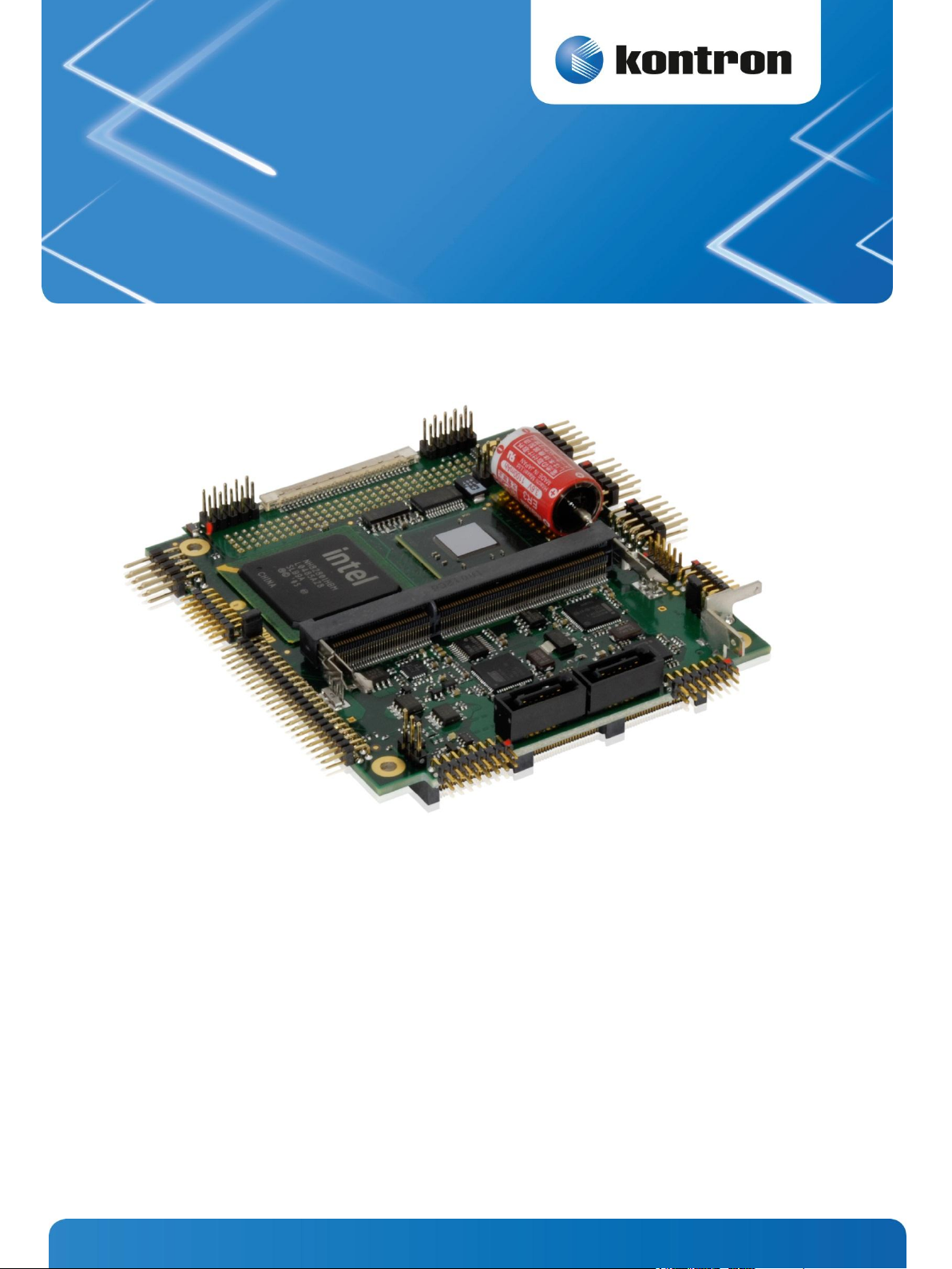
MSM-LP
Document Revision 105
» Kontron User’s Guide «
Page 2

MSM-LP / User Information
www.kontron.com
» Table of Contents «
1 User Information ............................................................................ 1
1.1 About this Document ............................................................................................................... 1
1.2 Copyright Notice ..................................................................................................................... 1
1.3 Trademarks ............................................................................................................................ 1
1.4 Standards .............................................................................................................................. 1
1.5 Warranty ............................................................................................................................... 1
1.6 Technical Support ................................................................................................................... 2
2 Specification ................................................................................. 3
2.1 Available Products ................................................................................................................... 3
2.2 Available Options .................................................................................................................... 3
2.3 Evaluation Kit ......................................................................................................................... 3
2.4 Block Diagram ........................................................................................................................ 4
2.5 Functional Specification ........................................................................................................... 5
2.6 Mechanical Specifications ......................................................................................................... 5
2.7 Electrical Specifications ............................................................................................................ 6
2.7.1 Supply Voltage ...................................................................................................................... 6
2.7.2 Supply Current (Windows XP SP3) .............................................................................................. 6
2.8 MSM-LP Environmental Specifications .......................................................................................... 6
2.9 External Real-Time Clock Battery ................................................................................................ 6
3 MSM-LP Connectors & Jumpers .......................................................... 8
3.1 Top ...................................................................................................................................... 8
3.2 Connector Descriptions – Top ................................................................................................... 10
3.2.1 CRT Interface – X50 .............................................................................................................. 10
3.2.2 SATA Interface – X70/X71 ...................................................................................................... 11
3.2.3 Serial Port Interfaces – X40/X41/X42/X43 ................................................................................. 12
3.2.4 GPIO and AD/DA Interface – X31 .............................................................................................. 13
3.2.5 Power Supply – X1 ................................................................................................................ 14
3.2.6 USB Interfaces – X50/X51 ...................................................................................................... 14
Page 3

MSM-LP / User Information
www.kontron.com
3.2.7 IDE Interface (P-ATA) – X77 .................................................................................................... 15
3.2.8 Fan Connector – X24 ............................................................................................................. 15
3.2.9 Audio Interface – X20 ........................................................................................................... 16
3.2.10 LAN Interface – X60/X61 ....................................................................................................... 16
3.2.11 AMP Power Input – X2/X3 ...................................................................................................... 17
3.2.12 LVDS Interface..................................................................................................................... 17
3.3 Bottom ............................................................................................................................... 18
3.4 Connector Descriptions – Bottom .............................................................................................. 20
3.4.1 LPC/POD Interface – X34 ........................................................................................................ 20
3.4.2 Backlight Connector – X12 ..................................................................................................... 20
3.5 Other Connectors .................................................................................................................. 21
3.6 Jumpers .............................................................................................................................. 21
3.6.1 THT Jumpers – Top ............................................................................................................... 21
4 Special Features ............................................................................ 22
4.1 KeAPI ................................................................................................................................. 22
4.2 INT15 Support ...................................................................................................................... 22
4.3 System Controller USB Serial Commands .................................................................................... 24
4.3.1 I/O Control Requests/Answers: ............................................................................................... 24
4.4 Digital I/O Ports/Operations .................................................................................................... 25
4.4.1 I/O Control Access ................................................................................................................ 25
4.5 Watchdog Function ................................................................................................................ 25
4.5.1 BIOS Setup ......................................................................................................................... 25
4.5.2 Watchdog Hardware Access .................................................................................................... 25
5 Design Considerations .................................................................... 29
5.1 Board Drill-Hole Dimensions .................................................................................................... 29
5.2 Thermal Management ............................................................................................................. 29
5.3 Heat Spreader Dimensions ...................................................................................................... 30
6 BIOS Operation ............................................................................. 31
6.1 Determining the BIOS Version .................................................................................................. 31
6.2 Setup Guide ......................................................................................................................... 31
6.2.1 Start the AMI Aptio® BIOS Setup Utility ..................................................................................... 31
6.3 BIOS Setup .......................................................................................................................... 33
Page 4

MSM-LP / User Information
www.kontron.com
6.3.1 Main Menu .......................................................................................................................... 33
6.3.2 Advanced Menu ................................................................................................................... 34
6.3.3 Chipset Menu ...................................................................................................................... 56
6.3.4 Boot Menu .......................................................................................................................... 62
6.3.5 Security Menu ..................................................................................................................... 63
6.3.6 Exit Menu ........................................................................................................................... 64
6.4 BIOS Update ........................................................................................................................ 65
7 Appendix A: Assembly Views ............................................................ 66
7.1 Top .................................................................................................................................... 66
7.2 Bottom ............................................................................................................................... 67
8 Appendix: Document Revision History ................................................ 68
Page 5

MSM-LP / User Information
www.kontron.com
1
1 User Information
1.1 About this Document
This document provides information about products from Kontron Europe GmbH and/or its subsidiaries. No warranty
of suitability, purpose, or fitness is implied. While every attempt has been made to ensure that the information in this
document is accurate, the information contained within is supplied “as-is” and is subject to change without notice.
For the circuits, descriptions and tables indicated, Kontron assumes no responsibility as far as patents or other rights
of third parties are concerned.
1.2 Copyright Notice
Copyright © 2003-2013 Kontron Europe GmbH
All rights reserved. No part of this document may be reproduced, transmitted, transcribed, stored in a retrieval
system, or translated into any language or computer language, in any form or by any means (electronic, mechanical,
photocopying, recording, or otherwise), without the express written permission of Kontron Europe GmbH.
1.3 Trademarks
MICROSPACE®, smartModule® and smartCore® are trademarks or registered trademarks of Kontron Europe GmbH.
Kontron is a trademark or registered trademark of Kontron AG.
The following lists the trademarks of components used in this product.
» IBM, XT, AT, PS/2 and Personal System/2 are trademarks of International Business Machines Corp.
» Microsoft is a registered trademark of Microsoft Corp.
» Intel is a registered trademark of Intel Corp.
All other products and trademarks mentioned in this manual are trademarks of their respective owners. For the
circuits, descriptions and tables indicated, Kontron assumes no responsibility as far as patents or other rights of third
parties are concerned.
1.4 Standards
Kontron Europe GmbH is certified to ISO 9000 standards.
1.5 Warranty
For this Kontron Europe GmbH product warranty for defects in material and workmanship exists as long as the
warranty period, beginning with the date of shipment, lasts. During the warranty period, Kontron Europe GmbH will
decide on its discretion if defective products are to be repaired or replaced.
Page 6

MSM-LP / User Information
www.kontron.com
2
Within the warranty period, the repair of products is free of charge as long as warranty conditions are observed.
Warranty does not apply for defects arising/resulting from improper or inadequate maintenance or handling by the
buyer, unauthorized modification or misuse, as well as the operation outside of the product´s environmental
specifications and improper installation and maintenance.
Kontron Europe GmbH will not be responsible for any defects or damages to other products not supplied by Kontron
Europe GmbH that are caused by a faulty Kontron Europe GmbH product.
1.6 Technical Support
Technicians and engineers from Kontron Europe GmbH and/or its subsidiaries are available for technical support. We
are committed to make our product easy to use and will help you use our products in your systems.
Please consult our Website at http://www.kontron.com/support for the latest product documentation, utilities,
drivers and support contacts. Consult our customer section http://emdcustomersection.kontron.com for the latest
BIOS downloads, Product Change Notifications, Board Support Packages, DemoImages, 3D drawings and additional
tools and software. In any case you can always contact your board supplier for technical support.
Page 7
MSM-LP / Specification
www.kontron.com
3
Part No.
Article
Intel® CPU
Remarks
802360
MSM-LP-D425
D425
PC/104 SBC with single-core Intel D425 processor
802350
MSM-LP-D525
D525
PC/104 SBC with dual-core Intel D525 processor
802361
MSM-LP-D425-sys
D425
PC/104 System with single-core Intel D425 processor
802351
MSM-LP-D525-sys
D525
PC/104 System with dual-core Intel D525 processor
Part No.
Article
Remarks
802365
RAM 1GB DDR3 SODIMM
802366
RAM 2GB DDR3 SODIMM
802367
RAM 4GB DDR3 SODIMM
802313
PCI104 Connector
802358
MSM-LP Heat Spreader Kit
Heat spreader, screw set included.
802314
MSM-PC104 Passive Cooler Kit
Passive cooler including assembly material.
802316
MSM-PC104 Active Cooler Kit
Heat sink and fan including assembly material.
802040
MSM-PC104 CK
Cablekit including:
Interfaces: DVI, Line-In/out or Mic-In, S/PDIF, 1Gb Ethernet
Cables: USB, VGA, COM single, SATA, LAN, audio, IDE
Warning: Do not use with system boards
The pin out is mirrored due to assembling of connectors on the bottom side!
Part No.
Article
Remarks
802359
MSM-LP-Evalkit
Ready to Run package including:
MSM-LP-D525,
MSM-LP Heat Spreader Kit, MSM-PC104 Active Cooler,
MSM-PC104 CK, PCI-104 Connector,
2GB SODIMM DDR3,
Power supply
250GB 2.5" SATA hard disk with:
Dual boot system Win XPe (Evaluation Version), Linux Fedora
Board Support Package
Test GUI for Win XPe, Linux
Documentation
2 Specification
2.1 Available Products
2.2 Available Options
2.3 Evaluation Kit
This kit is used for the evaluation of the MSM-LP product family and is ready-to-use.
Page 8
MSM-LP / Specification
www.kontron.com
4
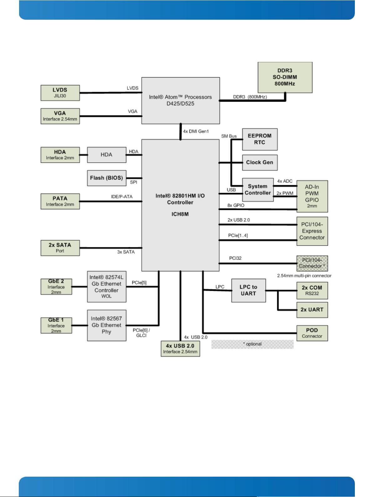
2.4 Block Diagram
Page 9

MSM-LP / Specification
www.kontron.com
5
2.5 Functional Specification
Processor
» CPU: Intel
®
D425 / D525
» Speed: 1.8GHz
Video
» Controller: Integrated graphics controller (CPU) multi-display support
» Memory: Up to 256MB (UMA)
» Drivers: Intel GMA
®
driver
Display Interfaces
» CRT Interface: Up to 2048 x 1536 @ 60Hz
» LCD Interface: Up to 1366 x 768, 18bpp
Interfaces
» 2x SATA
» PATA
» 2x Gbit LAN
» 4x USB 2.0
» 4x COM
» GPIO/ADC/PWM
» Audio
» PCI optional
» PCIexpress
Power Management
» S-States: S0, S3, S4, S5, S5eco
2.6 Mechanical Specifications
» 90.0mm x 102.0mm
» Height approx. 15.5mm
Page 10
MSM-LP / Specification
www.kontron.com
6
Mode
[A] 5V
[W]
Full load
2.8
14
average values
2.7 Electrical Specifications
2.7.1 Supply Voltage
» 5VDC ± 5%
2.7.2 Supply Current (Windows XP SP3)
The tested boards were mounted on a carrier board; a mouse and a keyboard were connected. The power-consumption
tests were executed under Windows XP SP3 by using a tool to stress the CPU (INTEL® Thermal Analysis Tool at 100 %
load). The power measurement values were acquired after 15 minutes at full load and a stable CPU die temperature. To
ensure a stable die temperature, a corresponding heat sink was used to hold the temperature under the critical trip
point.
MSM-LP-D425/D525
2.8 MSM-LP Environmental Specifications
Temperature
Operating with Kontron Compact Computers AG cooling solution:
» Standard operating temperature: 0 to +70°C
» Extended operating temperature: -40 to +85°C
» Storage temperature: -40 to +85°C
Note: In any case, the maximum operating temperature should never be exceeded!
Humidity
» Operating: 5% to 90% (non-condensing)
2.9 External Real-Time Clock Battery
» Nominal voltage: 3.6V
» Capacity: 1100mAh
Page 11

MSM-LP / Specification
www.kontron.com
7
CAUTION!
Danger of explosion if the battery is incorrectly
replaced. Replace only with the same or equivalent type
recommended by the manufacturer. Dispose of used
batteries according to the manufacturer's instructions.
VORSICHT!
Explosionsgefahr bei unsachgemässem Austausch der
Batterie. Ersatz nur durch denselben oder einem vom
Hersteller empfohlenen gleichwertigen Typ. Entsorgung
gebrauchter Batterien nach Angaben des Herstellers.
ATTENTION!
Risque d'explosion avec l'échange inadéquat de la
batterie. Remplacement seulement par le même ou un
type équivalent recommandé par le producteur.
L'évacuation des batteries usagées conformément à des
indications du fabricant.
PRECAUCION!
Peligro de explosión si la batería se sustituye
incorrectamente. Sustituya solamente por el mismo o
tipo equivalente recomendado por el fabricante.
Disponga las baterías usadas según las instrucciones del
fabricante.
ADVARSEL!
Lithiumbatteri – Eksplosionsfare ved fejlagtig
håndtering. Udskiftning må kun ske med batteri af
samme fabrikat og type. Levér det brugte batteri tilbage
til leverandøren.
ADVARSEL!
Eksplosjonsfare ved feilaktig skifte av batteri. Benytt
samme batteritype eller en tilsvarende type anbefalt av
apparatfabrikanten. Brukte batterier kasseres i henhold
til fabrikantens instruksjoner.
VARNING!
Explosionsfara vid felaktigt batteribyte. Använd samma
batterityp eller en ekvivalent typ som rekommenderas
av apparattillverkaren. Kassera använt batteri enligt
fabrikantens instruktion.
VAROITUS!
Paristo voi räjähtää, jos se on virheellisesti asennettu.
Vaihda paristo ainoastaan lalteval- mistajan
suosittelemaan tyyppiln. Hävitä käytetty paristo
valmistajan ohjeiden mukaisesti.
Lithium Battery Precautions:
Page 12

MSM-LP / MSM-LP Connectors & Jumpers
www.kontron.com
8
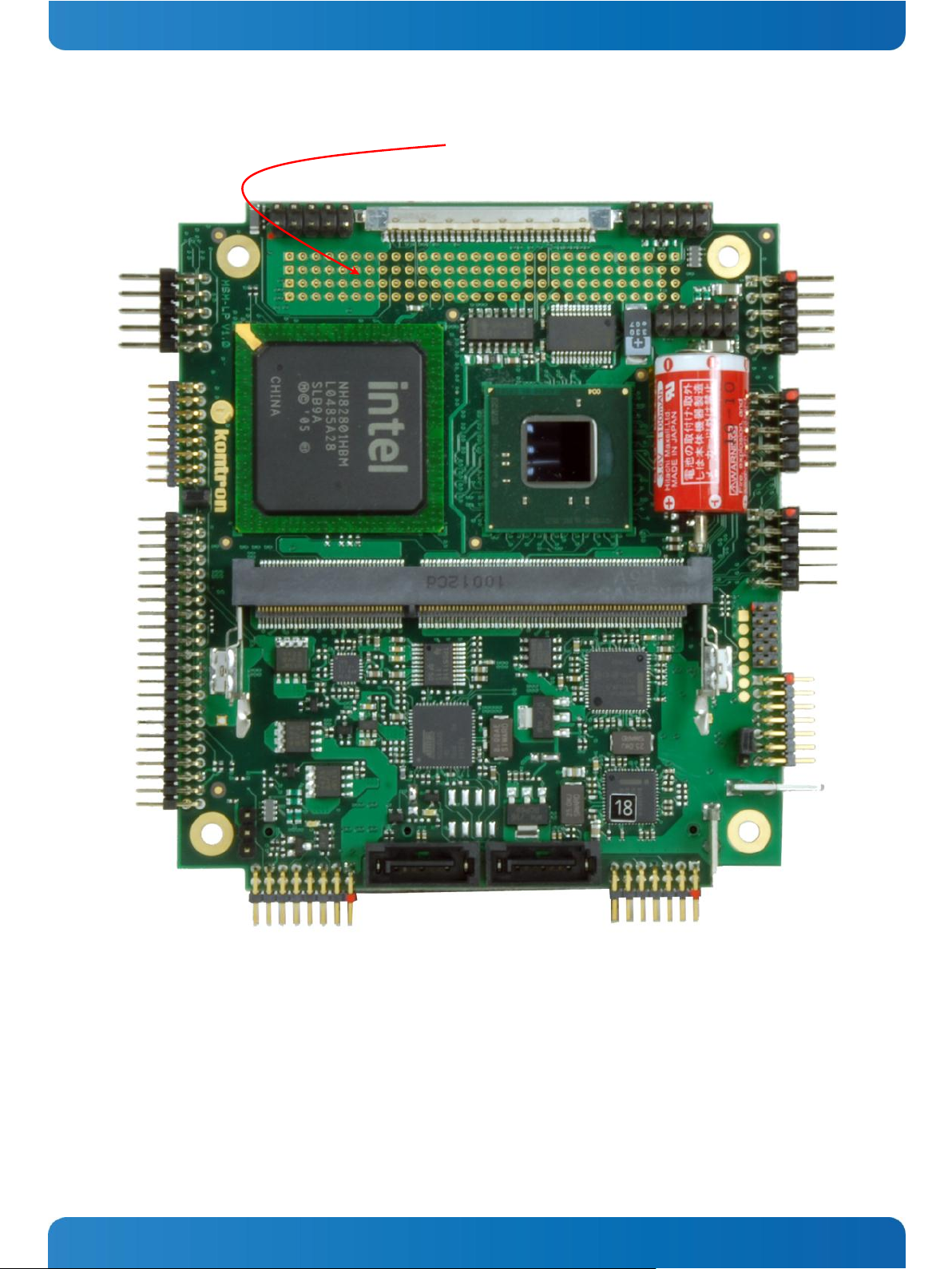
3 MSM-LP Connectors & Jumpers
3.1 Top
Page 13
MSM-LP / MSM-LP Connectors & Jumpers
www.kontron.com
9
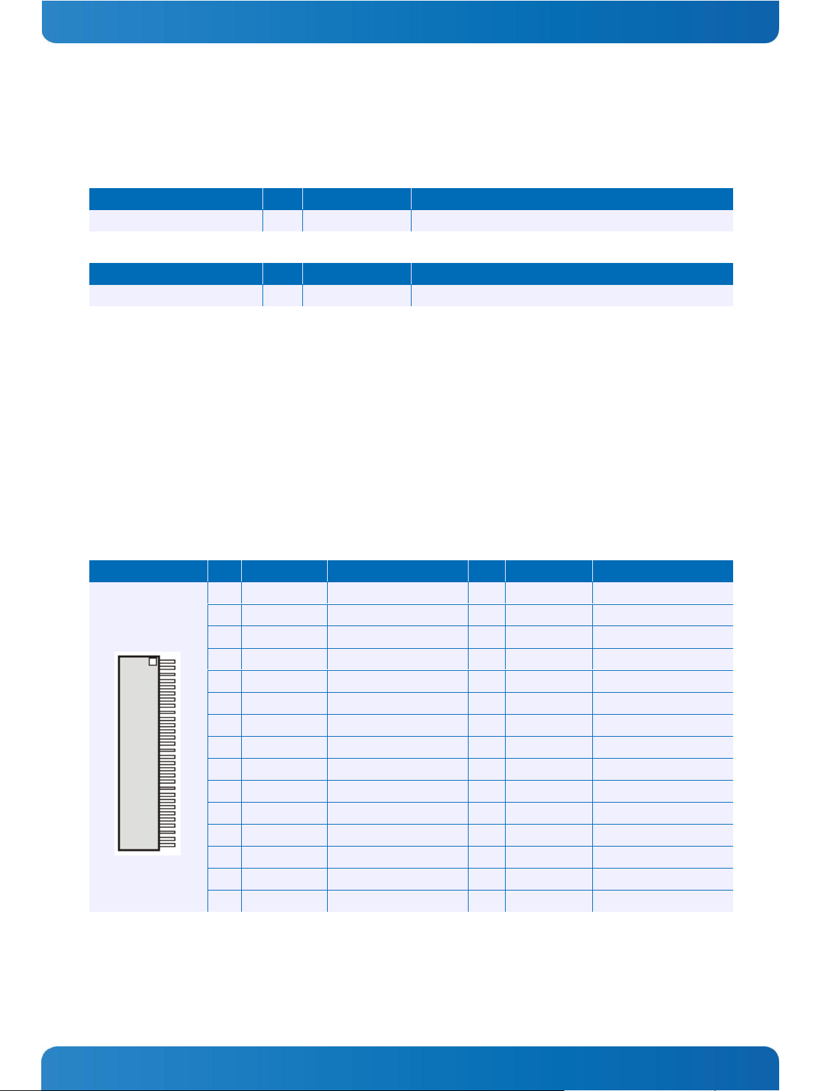
Photo of an MSM-LP board with optional PCI-104 (X101) connector assembled on the bottom (pins visible through the
board).
Page 14
MSM-LP / MSM-LP Connectors & Jumpers
www.kontron.com
10
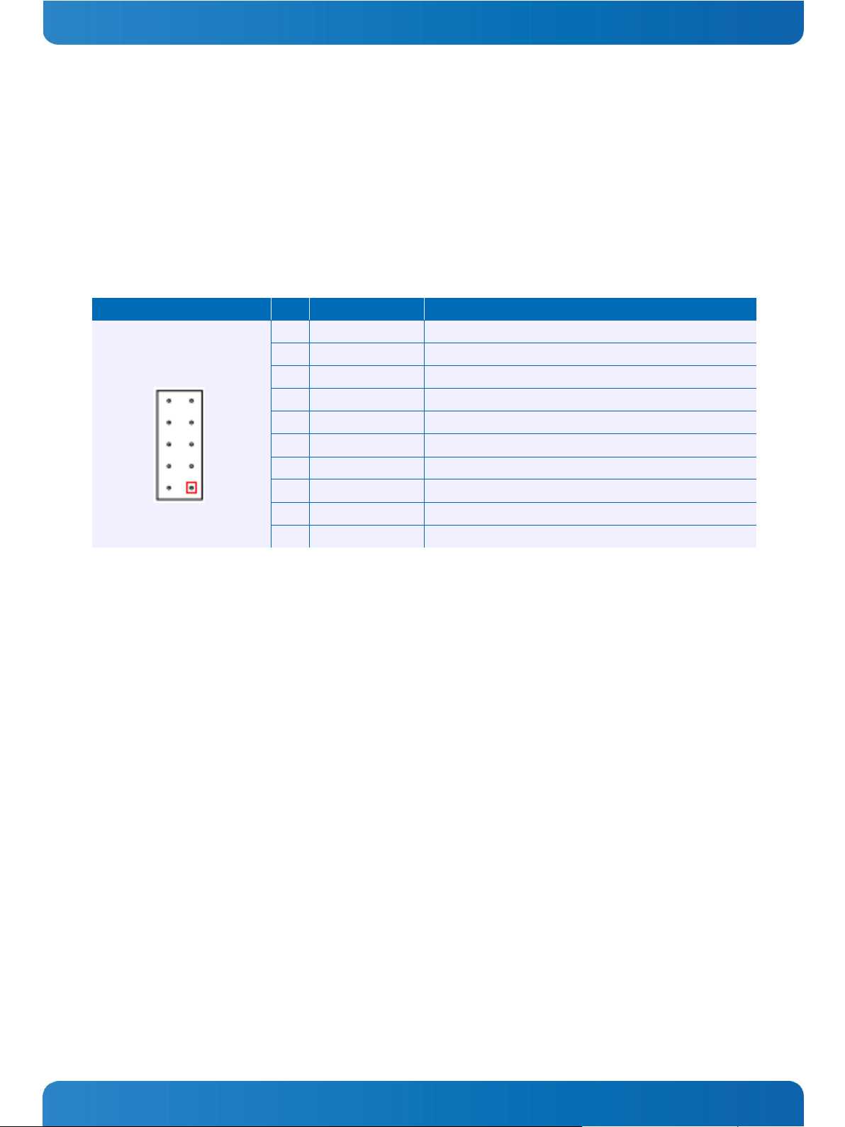
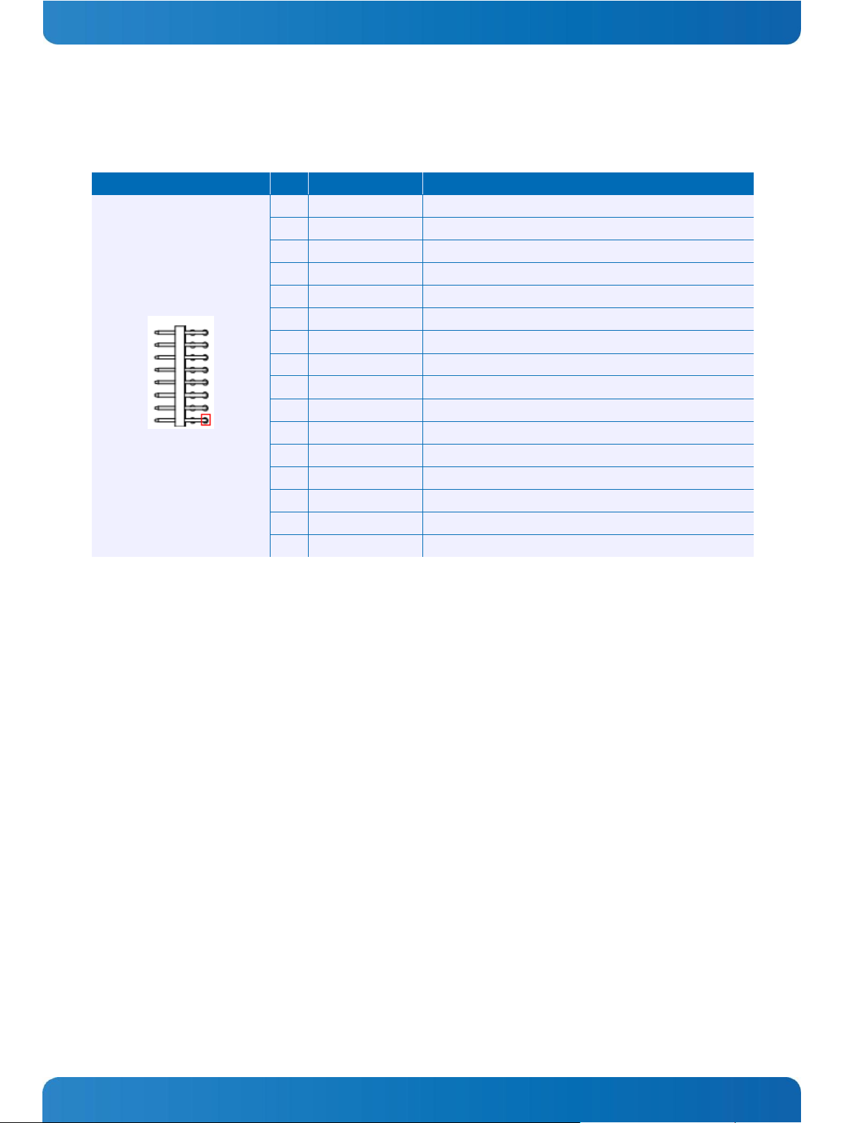
Header
Pin
Signal Name
Function
2.54mm grid
1
GND
Ground
2
RED
Red video signal
3
NC
Not connected
4
GREEN
Green video signal
5
NC
Not connected
6
BLUE
Blue video signal
7
CRT_DDATA
DDC data
8
CRT_HSYNC
Horizontal sync
9
CRT_VSYNC
Vertical sync
10
CRT_DCLK
DDC clock
3.2 Connector Descriptions – Top
Warning: On system boards the pin out is mirrored due to assembling of connectors on bottom side!
The description is applicable on view from top, if system pin headers are viewed from bottom; even and odd pin
numbers must be swapped 1<->2, 3<->4, 5<->6, 7<->8, 9<->10, 11<->12, 13<->14, 15<->16.
3.2.1 CRT Interface – X50
The board provides an onboard analogue CRT interface.
Page 15
MSM-LP / MSM-LP Connectors & Jumpers
www.kontron.com
11
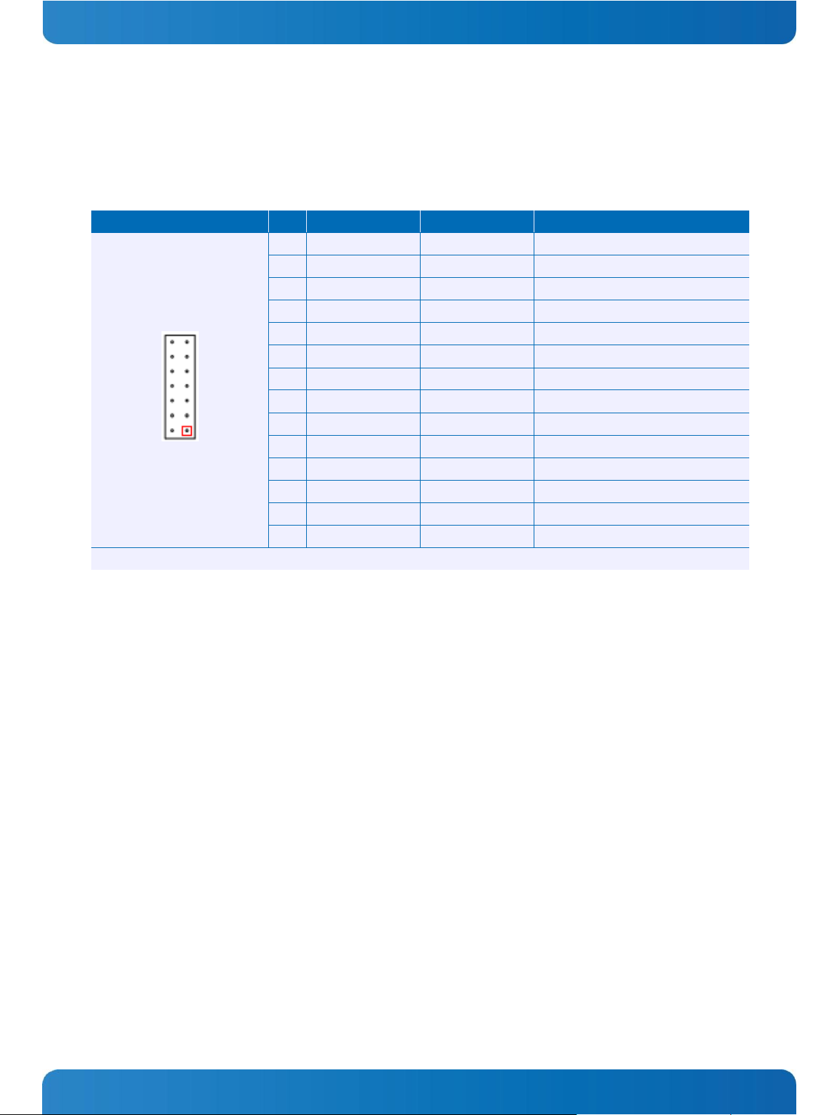
Header
Pin
Signal Name
SATA Connector Pin
Function
1.27mm grid
1
GND Ground
2
GND 1 Ground
3
SATAx_TXP
2
Data transmit positive
4
NC NC
5
SATAx_TXN
3
Data transmit negative
6
NC NC
7
GND Ground
8
GND 4 Ground
9
SATAx_RXN
5
Data receive negative
10
NC NC
11
SATAx_RXP
6
Data receive positive
12
NC NC
13
GND Ground
14
GND 7 Ground
x is the number of the SATA port (SATA1: x -> 1)
3.2.2 SATA Interface – X70/X71
The board layout supports two SATA 300 interfaces. It is not intended that the standard SATA connectors are
assembled from the bottom side. Any connections to a baseboard or to a system I/O must be done with standard
cables.
Page 16
MSM-LP / MSM-LP Connectors & Jumpers
www.kontron.com
12
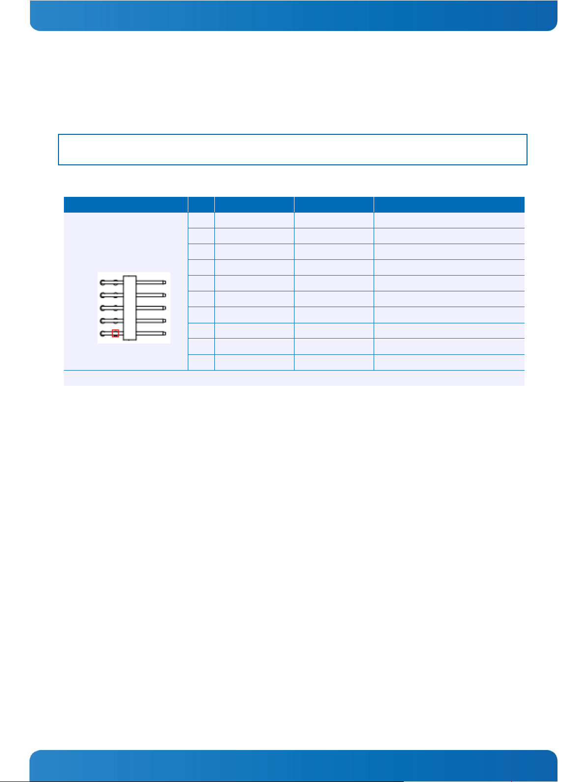
Header
Pin
Signal Name
Function
DSUB9
2.54mm grid
1
DCDXx#
Data carrier detect
1
2
DSRXx#
Data set ready
6
3
RXDXx#
Receive data
2
4
RTSXx#
Request to send
7
5
TXDXx#
Transmit data
3
6
CTSXx#
Clear to send
8
7
DTRXx#
Data terminal ready
4
8
RIXx#
Ring indicator
9 9 GND
Ground
5
10
V5.0_S0
Power +5V
-
x is the number of the COM port (COM1: x -> 1)
3.2.3 Serial Port Interfaces – X40/X41/X42/X43
Four serial ports for asynchronous serial communication are defined. X40, X41 support RS-232 level and X42, X43
support TTL level. An external conversion to RS-232 and RS-422/485 is possible for all ports.
Note: External converters to RS-232 or RS-422/485 with galvanic separation are available. All four ports can
bypass the level-shifters to support TTL levels (OEM high volume placement option).
On system board all four serial ports support TTL level!
Page 17
MSM-LP / MSM-LP Connectors & Jumpers
www.kontron.com
13
Header
Pin
Signal Name
Function
2.00mm grid
1
GPIO0
General purpose I/O
2
GPIO1
General purpose I/O
3
GPIO2
General purpose I/O
4
GPIO3
General purpose I/O
5
GPIO4
General purpose I/O
6
GPIO5
General purpose I/O
7
GPIO6
General purpose I/O
8
GPIO7
General purpose I/O
9
PWM_OUT0
D/A output
10
PWM_OUT1
D/A output
11
ADC_IN0
A/D input (0-10.3V) *)
12
ADC_IN1
A/D input (0-10.3V) *)
13
ADC_IN2
A/D input (0-10.3V) *)
14
ADC_IN3
A/D input (0-10.3V) *)
15
GND
Ground
16
+V3.3_S5
Power +3.3V
3.2.4 GPIO and AD/DA Interface – X31
The board has a GPIO header interface with additional AD/DA channels. Any filtering must be done externally.
*) A/D input (0-4.88V) on system board
Page 18
MSM-LP / MSM-LP Connectors & Jumpers
www.kontron.com
14
Header
Pin
Signal Name
Function
2.00mm grid
1
+12V_IN
Power +12V
2*)
PSON#
ATX power on (Power LED)
3
+5V_IN
Power +5V
4
+5V_IN
Power +5V
5
GND
Ground
6
GND
Ground
7
GND
Ground
8
GND
Ground
9
POWER_BTN#
External main button
10
RESET_BTN#
External reset button
11*)
IGNITION#
Ignition input
12
HDD_ACT#
HDD activity LED
13
VBAT
RTC battery input
14
SMB_ALERT#
System management alert
15
SMB_DAT
System management bus data
16
SMB_CLK
System management bus clock
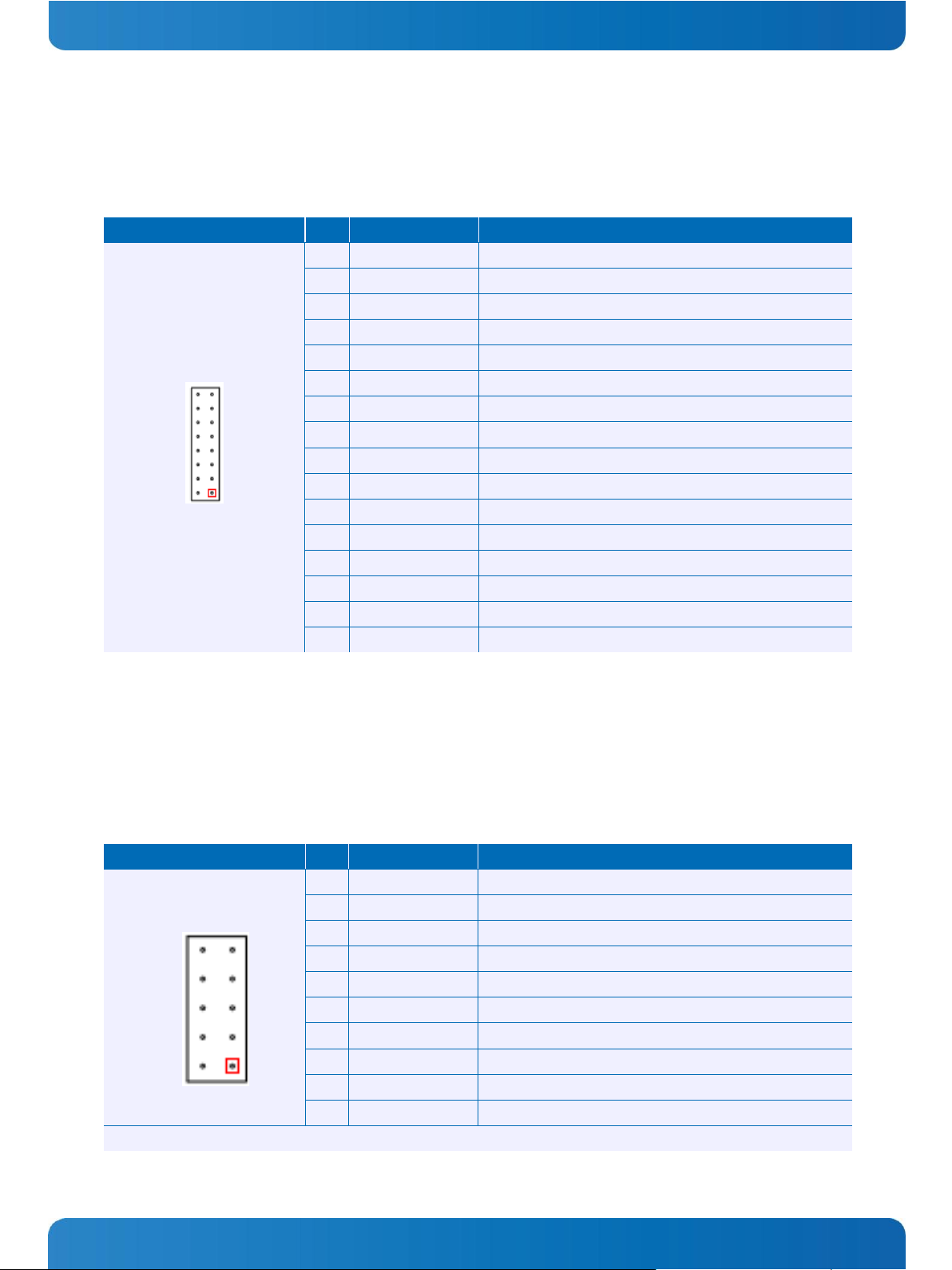
Header
Pin
Signal Name
Function
2.54mm grid
1
USBxVCC
Power +5V
2
USByVCC
Power +5V
3
USBxN
USBx data negative
4
USByN
USBy data negative
5
USBxP
USBx data positive
6
USByP
USBy data positive
7
GND
Ground
8
GND
Ground
9
SHD
Shield
10
SHD
Shield
x (y) is the number of the USB port (USB1: x -> 1)
3.2.5 Power Supply – X1
A power connector for the main power supply is provided. The SBCs function with a single +5V power supply.
Additional voltages for PC/104 peripherals (+12V, -5V, -12V) must be generated externally.
*) Warning: On system board the pin out changes!
Pin 2 PSON# is the SLP_S5# 3.3 Volt output and Pin 11 EC_IGNITION# is the SLP_S3# 3.3 Volt output.
3.2.6 USB Interfaces – X50/X51
The board is populated with four USB interfaces. Two connectors with 2 USB ports each are defined. Further USB ports
are accessible over the PCIe/104 extension connector.
Page 19
MSM-LP / MSM-LP Connectors & Jumpers
www.kontron.com
15
Header
Pin
Signal Name
Function
Pin
Signal Name
Function
2.54mm grid
1
IDE_RST#
Reset
2
GND
Ground
3
IDE_D7
Data 7
4
IDE_D8
Data
5
IDE_D6
Data 6
6
IDE_D9
Data
7
IDE_D5
Data 5
8
IDE_D10
Data
9
IDE_D4
Data 4
10
IDE_D11
Data
11
IDE_D3
Data 3
12
IDE_D12
Data
13
IDE_D2
Data 2
14
IDE_D13
Data
15
IDE_D1
Data 1
16
IDE_D14
Data
17
IDE_D0
Data 0
18
IDE_D15
Data
19
GND
Ground
20
Key (NC)
Key pin
21
IDE_DRQ
DMA request
22
GND
Ground
23
IDE_IOW#
I/O write
24
GND
Ground
25
IDE_IOR#
I/O read
26
GND
Ground
27
IDE_IOCHRDY
I/O channel ready
28
IDE_CSEL
Cable select
29
IDE_DACK#
DMA acknowledge
30
GND
Ground
31
IDE_IRQ
Interrupt request
32
NC
Not connected
33
IDE_SA1
Address 1
34
IDE_ATAD
UDMA detection
35
IDE_SA0
Address 0
36
IDE_SA2
Address 2
37
IDE_CS1#
Chip select 1
38
IDE_CS3#
Chip select 3
39
NC
Not connected
40
GND
Ground
41
VCC
Power +5V
42
VCC
Power +5V
43
GND
Ground
44
NC
Not connected
Header
Pin
Signal Name
Function
2.00mm
1
Speed frequency signal
2
+5V
Power +5V
3
GND
Ground
3.2.7 IDE Interface (P-ATA) – X77
The design supports one IDE interface that can drive up to two hard disks. When two devices share a single adapter,
they must be connected in a master-slave, daisy-chain configuration.
X77 not equipped on system board.
3.2.8 Fan Connector – X24
Page 20
MSM-LP / MSM-LP Connectors & Jumpers
www.kontron.com
16
Header
Pin
Signal Name
Function
2.00mm grid
1
LINE_R
Line right
2
GND_A
Analogue ground
3
LINE_L
Line left
4
MIC_R
Mic right
5
GND_A
Analogue ground
6
MIC_L
Mic left
7
V5
Power +5V
8
SPDIF_IN
Digital audio input
9
GND
Ground
10
SPDIF_OUT
Digital audio output
Header
Pin
Signal Name
Function
2.00mm grid
1
GbEx_MDI0N
Bidirectional pair 0 negative
2
GbEx_MDI0P
Bidirectional pair 0 positive
3
GbEx_MDI1N
Bidirectional pair 1 negative
4
GbEx_MDI1P
Bidirectional pair 1 positive
5
GbEx_LED0
LED Link
6
V1.8
Center voltage
7
GND
Ground
8
V3.3
Power +3.3V
9
GbEx_LED1
LED activity
10
GbEx_LED2
LED link 100
11
GbEx_MDI2N
Bidirectional pair 2 negative
12
GbEx_MDI2P
Bidirectional pair 2 positive
13
GbEx_MDI3N
Bidirectional pair 3 negative
14
GbEx_MDI3P
Bidirectional pair 3 positive
x is the number of the GbE port (GbE1: x -> 1)
3.2.9 Audio Interface – X20
The audio interface provides stereo analogue and digital audio signals.
3.2.10 LAN Interface – X60/X61
Two Gbit Ethernet ports are defined. Suitable transformers must be provided externally.
Page 21
MSM-LP / MSM-LP Connectors & Jumpers
www.kontron.com
17
Header
Nr.
Signal Name
Function
AMP 2.8mm
X3
V5.0_IN
5 Volt power IN
Header
Nr.
Signal Name
Function
AMP 4.75mm
X2
GND
Ground
Header
Pin
Signal Name
Function
Pin
Signal Name
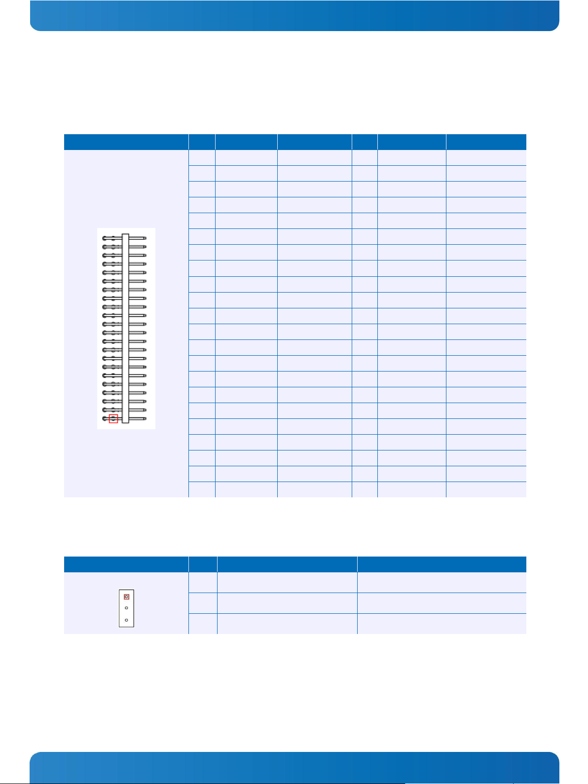
Function
1
FPC_AN
First channel data out A
16
NC
Not connected
2
FPC_AP
First channel data out A
17
GND
Ground
3
FPC_BN
First channel data out B
18
NC
Not connected
4
FPC_BP
First channel data out B
19
NC
Not connected
5
FPC_CN
First channel data out C
20
NC
Not connected
6
FPC_CP
First channel data out C
21
NC
Not connected
7
GND
Ground
22
NC
Not connected
8
FPC_CLKN
First channel clock
23
NC
Not connected
9
FPC_CLKP
First channel clock
24
GND
Ground
10
FPC_DN
First channel data out D
25
SDA
I2C data line
11
FPC_DP
First channel data out D
26
DATAENA
Panel power output
12
NC
Not connected
27
SCL
I2C clock line
13
NC
Not connected
28
VCC
+3.3V power *)
14
GND
Ground
29
VCC
+3.3V power *)
15
NC
Not connected
30
VCC
+3.3V power *)
3.2.11 AMP Power Input – X2/X3
The AMP power inputs are always connected on the top side of the board.
X2 and X3 not equipped on system board.
3.2.12 LVDS Interface
The LVDS implementation complies with the JILI specification of Kontron (JILI30). When using an LCD, additional
voltages may be required to drive the display logic and supply the backlight converter therefore an additional
connector for supply voltages is provided.
The FPC connector is only mounted on the top side. The corresponding backlight connector is assembled on the
opposite side.
FPC Connector – X11
*) Panel power can be set to +5V by assembly option.
Page 22
MSM-LP / MSM-LP Connectors & Jumpers
www.kontron.com
18
3.3 Bottom
Page 23

MSM-LP / MSM-LP Connectors & Jumpers
www.kontron.com
19
Photo of an MSM-LP board with optional PCI-104 (X101) connector assembled.
Page 24

MSM-LP / MSM-LP Connectors & Jumpers
www.kontron.com
20
Header
Pin
Signal Name
Function
Pin
Signal Name
Function
2.00mm grid
1
V3.3_S0
Power
2
LPC_LDA0
Data
3
LFRAME#
LPC frame
4
LPC_LDA1
Data
5
PLT_RST#
Reset OUT
6
LPC_LDA2
Data
7
V3.3_S0
Power
8
LPC_LDA3
Data
9
V5.0_S0
Power
10
PLT_RST#
Reset OUT
11
CLK
Clock
12
BIOS_EN
BIOS selection
13
GND
Ground
14
RESET_IN#
Reset IN
15
V3.3_SPI_PROG
Power IN
16
SERIRQ
17
SPI_CS#
18
SPI_CLK
19
SPI_MISO
20
SPI_MOSI
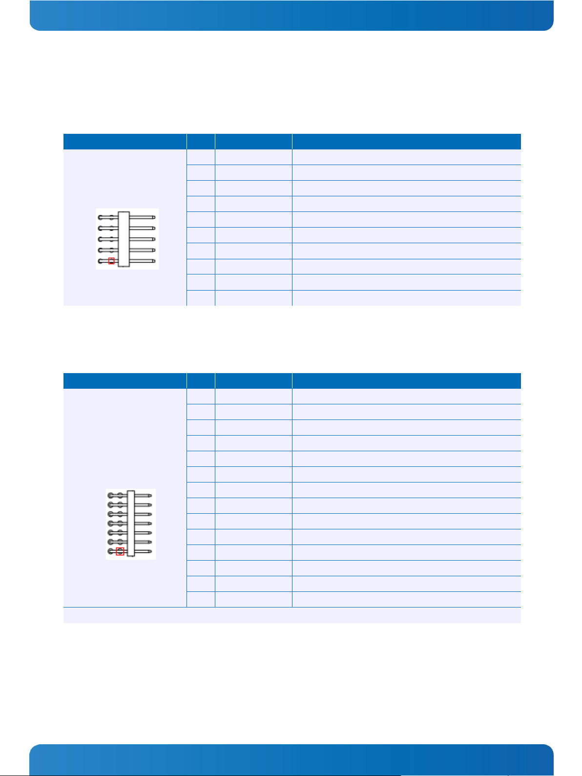
Header
Pin
Signal Name
Function
1
NC
Not connected
2
BKLTADJ
Brightness control (PWM 3.3 V)
3
GND
Ground
4
NC
Backlight power +5V *)
5
NC
Backlight power +5V *)
6
GND
Ground
7
BKLTON
Backlight on/off
3.4 Connector Descriptions – Bottom
3.4.1 LPC/POD Interface – X34
This is a connector for additional LPC devices such as POD, SuperIO or TPM. It can also be used for a second BIOS flash
interface (SPI or LPC)
3.4.2 Backlight Connector – X12
The backlight connector is always mounted on the bottom side, opposite of the LVDS FPC Connector .
*) Backlight power can be set to +12V by assembly option (needs +12V on pin 1 of supply connector X1).
Page 25

MSM-LP / MSM-LP Connectors & Jumpers
www.kontron.com
21
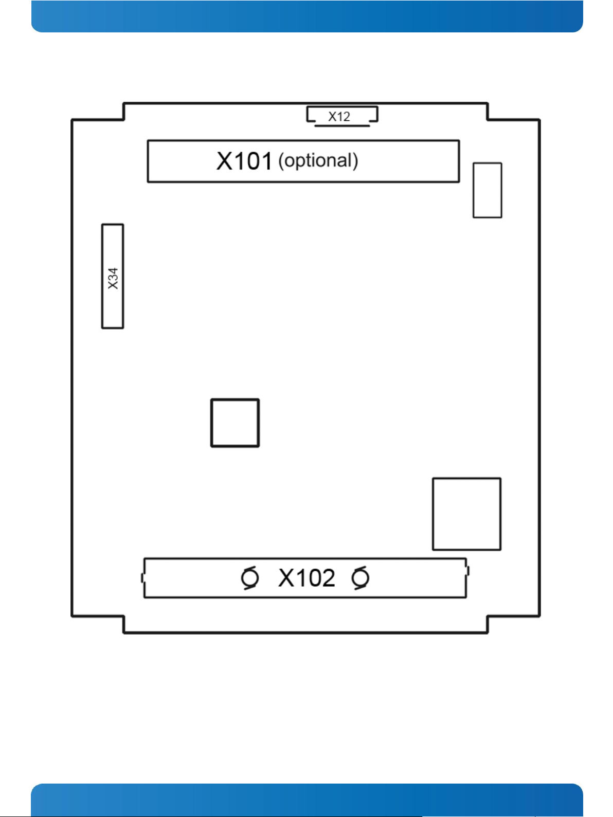
Connector
Structure
Pins
Remarks
X101
PCI-104
4x30
Bottom, 2mm (optional)
X17
JTAG G-LAN1
1x7
Top, 2mm
X105
SODIMM DDR3
204
Top, 0.6mm
X25
AVR programming
2x4
Top, 2mm
X102
PC104e
156
Bottom, 0.635mm
Assembly Defaults
Description
Reference
Sort
Position
Signal Name
Open / Position 1-2
Closed / Position 2-3
X14 *)
3-way 2.0 mm
2-3
V3.3_82574
WOL *)
No WOL
X32
2-way 2.0 mm
Closed
Auto-start
No auto-start
Auto-start
X35
2-way 2.0 mm
open
BIOS_Default
Normal BIOS startup
Recovery BIOS settings
3.5 Other Connectors
3.6 Jumpers
3.6.1 THT Jumpers – Top
Settings written in bold are defaults!
*) On system board WOL is always active, X14 is not equipped.
Page 26

MSM-LP / Special Features
www.kontron.com
22
4 Special Features
4.1 KeAPI
The Kontron embedded API (KeAPI) is an extension of the PICMG EAPI mainly with additional remote functionality. It
consists of hardware drivers providing access to features like Watchdog, I2C Bus or GPIO and a QT based user interface
KEAPI GUI. KeAPI is part of standard BSPs.
Please refer to EMD Customer Section for detailed documentation and downloads.
4.2 INT15 Support
The INT15 SFR (Special Function Register) functions support access to an I2C EEPROM. Addresses 0h-3FFh are reserved
for manufacturer information and counters; addresses 400h-7FFh are for customer purposes. INT15 SFR is supported
under DOS and Windows (over 32/64 bits driver).
Page 27

MSM-LP / Special Features
www.kontron.com
23
Page 28

MSM-LP / Special Features
www.kontron.com
24
4 Byte Command
Parameters
Description
'\x15','a','c',N
{0x15,0x61,0x63,N}
N-channels mask
N=0 – stop measurement
N=0x01...0x0F define which
channels 0...3 will be
measured
Start cyclic ADC measurement when ADC measures all channels
defined in the mask field, the controller sends an answer:
'\x15','D',VS...VE {0x15,0x44,VS…VE} ,
where VS is the Byte value of the first defined channel and VE is the
Byte value of the last defined channel.
The measurement/answer will repeat until the controller receives a
stop command ('\x15','a','c',0).
The number of received Bytes defined by the channels mask.
Example: mask N=0x05, ADC will measure on Channels 0 and 2 and
send a 4 Byte answer '\x15','D',V0,V2, where V0 and V2 are results
of the measurement on the appropriate channels.
'\x15','a','s',N
{0x15,0x61,0x73,N}
N-channels mask
N=0 – stop measurement
N=0x01...0x0F define which
channels 0...3 will be
measured
Start single shot ADC measurement when ADC measures all channels
defined in the mask field, the controller sends an answer:
'\x15','D',NS...NE {0x15,0x44,VS…VE}
where VS is the Byte value of the first defined channel and VE is the
Byte value of the last defined channel.
A non-cycled variant of the command above.
The number of received Bytes defined by the channels mask.
'\x15','p','a','e'
{0x15,0x70,0x61,0x65}
Enable PWM Channel A.
'\x15','p','a','d'
{0x15,0x70,0x61,0x64}
Disable PWM Channel A.
'\x15','p','b','e'
{0x15,0x70,0x62,0x65}
Enable PWM Channel B.
'\x15','p','b','d'
{0x15,0x70,0x62,0x64}
Disable PWM Channel B.
'\x15','w','a',N
{0x15,0x77,0x61,N}
N – PWM value
Set PWM value on Channel A (PWM must be enabled).
'\x15','w','b',N
{0x15,0x77,0x62,N}
N – PWM value
Set PWM value on Channel B (PWM must be enabled).
'\x15','f','v','r'
{0x15,0x66,0x76,0x72}
Get firmware version.
Answer: '\x15','V','M','S','M','L','P','_','0','6',0
The answer is always 11 Bytes, '\x15','V' - answer prefix, 8 Bytes of
the firmware version and a final Byte 0.
4.3 System Controller USB Serial Commands
Note: "System Controller USB" function must be enabled in the BIOS setup for using the ADC and PWM functions.
MSM-LP on-board 4-channel ADC and 2-channel PWM are accessible over a USB-serial port interface.
» In the Windows Device Manager it is represented as "KCC ADC/PWM Control Serial Interface". For a driver
installation under Windows, the "KCCUSBserial.inf" file is required.
» For Linux this interface does not require any drivers and is listed in the system as the "ttyACM0" serial port.
» Communication with ADC/PWM can be organized over the standard serial asynchronous protocol.
» Every control request consists of a 4 Byte package, with the leading (synch) Byte always 0x15.
» The number of Bytes in the answer is variable and depends on the request.
4.3.1 I/O Control Requests/Answers:
Page 29

MSM-LP / Special Features
www.kontron.com
25
Address
Name
Type
Description
0x4E
IND
RW
Indexed register access number
0x4F
DAT
RW
Indexed register content
4.4 Digital I/O Ports/Operations
The MSM-LP board has 8 digital inputs/outputs accessible over system port I/O operations.
The base address for I/O operations can be obtained as a WORD value from the PCI config space.
Bus:0, Dev:0x1F, Fun:0, Offset :0x48. Default base address is 0x0480.
4.4.1 I/O Control Access
Access to digital inputs/outputs, i.e. settings of I/O direction and logical level control can be provided over Kontron
embedded API functions.
4.5 Watchdog Function
The MSM-LP provides a watchdog function which resets the system when a specific amount of time has elapsed
without watchdog reset activity. The watchdog is highly configurable and the timeout time can be set between two
seconds and 65,535 seconds. The watchdog output is connected to the system controller.
4.5.1 BIOS Setup
With this setting, the watchdog timer of the MSM-LP can be enabled and the time until a reset is asserted can be
selected. The watchdog timer is part of F81216 chip and can be reset by directly accessing the F81216.
See Section Fehler! Verweisquelle konnte nicht gefunden werden. on how to access the F81216 watchdog.
Set Watchdog timeout:
» Disabled: The watchdog timer is disabled
» 1 / 5 / 15min: The watchdog timer resets the board after this amount of time.
» Default value: Disabled.
Warning: If this setting is enabled without a working watchdog reset in your program, your computer will reset after
the time set in the BIOS setup.
4.5.2 Watchdog Hardware Access
The watchdog registers of the F81216 chip are accessible over I/O mapped registers with indexed access. The
following table shows the addresses used. The F81216 chip has few devices and the watchdog is device number 8.
Page 30

MSM-LP / Special Features
www.kontron.com
26
Index
Bit
Name
Access
Function
0x30 0 WDT_EN
RW
Watchdog device enable register: 0=disable,1=enable
0x30
1-7 RsvdP
Reserved
0xF0 0 WDT_EVENT
RO
0: no time out has occurred
1: time out has occurred
Writing "1" to this bit will clear the status
0xF0
1-2
WDT_UNIT
RW
00: Timer Unit is 10ms
01: Timer Unit is 1 second
10: Timer Unit is 1 minute
11: reserved
0xF0
3-7 RsvdP
Reserved
0xF1
7-0
WDT_CNT
RW
The number of time units for the watchdog timer.
Write the same non-zero value twice to enable the timer; otherwise the timer is
disabled.
Attribute
Description
RsvdP
RESERVED AND PRESERVED
Reserved for future RW implementations. Registers are Read-only and the software must preserve the value for
writes to this bit.
RW
READ-WRITE REGISTER
Register bits are Read-Write and can be set or cleared by software.
RO
READ-ONLY
Register bits are Read-only and can not be altered by software.
WO
WRITE-ONLY
Register bits can only be Written. Reading returns indeterminable data.
Indexed Register Map of Watchdog Device 08h
Register Attributes
Page 31

MSM-LP / Special Features
www.kontron.com
27
Example: Enable/Retrigger Watchdog
; Watchdog device activation
mov dx, 4Eh ; Store port in dx for in/out instruction
mov al, 77h ; Configuration mode value
out dx, al ; Output 2 times to enter config mode
out dx, al ;
mov al, 07h ; Device number register
out dx, al ; Move value to IND register
inc dx ; Increment dx to DAT register = 0x4F
mov al, 08h ; Device number 8 - watchdog
out dx, al ; Set DAT register
dec dx ; Decrement dx to IND register
mov al, 30h ; Activation register address = 0x30
out dx, al ; Move value to IND register
inc dx ; Increment dx to DAT register
mov al, 01h ; Activation value WDT_EN = 1
out dx, al ; Set DAT register – enable watchdog device
dec dx ; Decrement dx to IND register to 0x4E address
mov al, 0F0h ; WDT_UNIT register
out dx, al ; Move value to IND register
inc dx ; Increment dx to DAT register to 0x4F address
mov al, 02h ; Set Timer Unit is 1 second, WD_UNIT = 01
out dx, al ; Set DAT register
dec dx ; Decrement dx to IND register to 0x4E address
mov al, 0F1h ; WDT_CNT register
out dx, al ; Move value to IND register
inc dx ; Increment dx to DAT register 0x4F address
mov al, 10 ; Set Timer to 10 second interval
out dx, al ; Set DAT register 2 times
out dx, al ;
dec dx ; Decrement dx to IND register to 0x4E address
mov al, 0AAh ; Leave configuration mode
out dx, al ; Move value to IND register
In C language:
outportb(0x4E,0x77); //output 2 times to enter configuration mode
outportb(0x4E,0x77);
outportb(0x4E,0x7); //device index
outportb(0x4F,0x8); //device number 8
outportb(0x4E,0x30); //activation register
outportb(0x4F,0x01); //activate watchdog WDT_EN = 1
outportb(0x4E,0xF0); //WDT_UNIT register
outportb(0x4F,0x02); //set timer unit is 1 second, WD_UNIT = 01
outportb(0x4E,0xF1); //WDT_CNT register
outportb(0x4F,10); // Set Timer to 10 second interval, 2 times
outportb(0x4F,10); //
outportb(0x4E,0xAA); //Leave configuration mode
Page 32

MSM-LP / Special Features
www.kontron.com
28
Example: Disable Watchdog
; Watchdog device activation
mov dx, 4Eh ; Store port in dx for in/out instruction
mov al, 77h ; Configuration mode value
out dx, al ; Output 2 times to enter config mode
out dx, al ;
mov al, 07h ; Device number register
out dx, al ; Move value to IND register
inc dx ; Increment dx to DAT register = 0x4F
mov al, 08h ; Device number 8 - watchdog
out dx, al ; Set DAT register
dec dx ; Decrement dx to IND register
mov al, 0F1h ; WDT_CNT register
out dx, al ; Move value to IND register
inc dx ; Increment dx to DAT register 0x4F address
mov al, 0 ; Set Timer to 10 second interval
out dx, al ; Set DAT register 2 times to disable watchdog
out dx, al ;
dec dx ; Decrement dx to IND register
mov al, 30h ; Activation register address = 0x30
out dx, al ; Move value to IND register
inc dx ; Increment dx to DAT register
mov al, 0h ; Deactivation value WDT_EN = 0
out dx, al ; Set DAT register – enable watchdog device
dec dx ; Decrement dx to IND register to 0x4E address
mov al, 0AAh ; Leave configuration mode
out dx, al ; Move value to IND register
In C language:
outportb(0x4E,0x77); //output 2 times to enter configuration mode
outportb(0x4E,0x77);
outportb(0x4E,0x7); //device index
outportb(0x4F,0x8); //device number 8
outportb(0x4E,0xF1); //WDT_CNT register
outportb(0x4F,0); // Set Timer to 0, 2 times
outportb(0x4F,0); //
outportb(0x4E,0x30); //activation register
outportb(0x4F,0x00); //deactivate watchdog WDT_EN = 0
outportb(0x4E,0xAA); //Leave configuration mode
Page 33

MSM-LP / Design Considerations
www.kontron.com
29
5 Design Considerations
5.1 Board Drill-Hole Dimensions
The MSM-LP board follows the PCIe/104TM specification. For more information see the PCI/104-ExpressTM & PCIe/104TM
specifications.
5.2 Thermal Management
The heat spreader plate assembly is delivered by Kontron Compact Computers AG for the MSM-LP. The heat spreader
plate on top of this assembly is not a heat sink. It works as a standard thermal interface to be used with a heat sink or
other cooling device.
External cooling must be provided to maintain the heat spreader plate at proper operating temperatures. Under worst
case conditions, the cooling mechanism must maintain an ambient air and heat spreader plate temperature of 85°C or
less.
The aluminum blocks and thermal pads on the underside of the heat spreader assembly serve to provide thermal
interfaces between the heat spreader plate and the major heat-generating components on the MSM-LP.
Page 34

MSM-LP / Design Considerations
www.kontron.com
30
5.3 Heat Spreader Dimensions
Figures: heat spreader plate showing the pads for the heat-generating components of the MSM-LP boards.
Page 35

MSM-LP / BIOS Operation
www.kontron.com
31
Setup Screen
Location
Function
Menu Bar
Top
Lists and selects all top level menus.
Legend Bar
Bottom right
Lists Setup navigation keys.
Item-Specific Help Window
Top right
Help for the selected item.
Menu Window
Center left
Selection fields for the current menu.
6 BIOS Operation
The module is equipped with the AMI Aptio® BIOS located in an onboard SPI serial flash memory. The BIOS can be
updated using a flash utility.
6.1 Determining the BIOS Version
The AMI Aptio® BIOS version can be determined on the BIOS setup screen.
6.2 Setup Guide
System behavior can be modified by changing the BIOS configuration.
Note: Selecting incorrect values may cause system boot failure. To recover, press <F3> to load setup default values.
6.2.1 Start the AMI Aptio
®
BIOS Setup Utility
To start the AMI Aptio® BIOS setup utility, press <DEL> during boot-up.
Press <DEL> to enter setup.
The Main Menu then appears.
The Setup Screen is composed of several sections:
Temporary Boot Menu
By pressing the <F7> key at the beginning of the startup process the temporary boot menu will appear.
Page 36

MSM-LP / BIOS Operation
www.kontron.com
32
Key
Function
or Arrow key
Select Screen
or Arrow key
Select Item
Enter
Select
+/-
Change Option
<F1>
General Help
<F2>
Previous Values
<F3>
Optimized Defaults
<F4>
Save and Exit
<F7>
Temporary Boot Menu
<ESC>
Exit
Menu Bar
The menu bar at the top of the window lists the different menus. Use the left/right arrow keys to make a selection.
Legend for Menu Bar
Selecting an Item
Use the or key to move. Use the + and – keys to select a value.
Displaying Submenus
Use the or key to move the cursor to the submenu then press <Enter>. The pointer () marks all the submenus.
Item-Specific Help Window
The Help window on the right side of each menu displays the Help text for the selected item.
General Help Window
Pressing <F1> on a menu brings up the general Help. Press <Esc> to exit.
Page 37

MSM-LP / BIOS Operation
www.kontron.com
33
6.3 BIOS Setup
6.3.1 Main Menu
Page 38

MSM-LP / BIOS Operation
www.kontron.com
34
6.3.2 Advanced Menu
Page 39

MSM-LP / BIOS Operation
www.kontron.com
35
Feature
Options
Description
PCI ROM Priority
Legacy ROM
EFI Compativle ROM
In case of multiple Option ROMs (Legacy and EFI
Compatible), specifies what PCI Option ROM to launch.
PCI Latency Timer
32 PCI Bus Clocks
64 PCI Bus Clocks
96 PCI Bus Clocks
…
248 PCI Bus Clocks
Value to be programmed into PCI Latency Timer Register.
VGA Palette Snoop
Disabled
Enabled
Enables or Disables VGA Palette Register Snooping.
PERR# Generation
Disabled
Enabled
Enables or Disables PCI Device to Generate PERR#.
SERR# Generation
Disabled
Enabled
Enables or Disables PCI Device to Generate SERR#.
PCI Subsystem Settings Menu
Page 40

MSM-LP / BIOS Operation
www.kontron.com
36
Feature
Options
Description
Relaxed Ordering
Disabled
Enabled
Enables or Disables PCI Express Device Relaxed Ordering.
Extended Tag
Disabled
Enabled
If Enabled allows Device to use 8-bit Tag field as a requester.
No Snoop
Disabled
Enabled
Enables or Disables PCI Express Device No Snoop Option.
Maximum Payload
Auto
128 Bytes
…
4096 Bytes
Set Maximum Payload of PCI Express Device or allow System
BIOS to select the value.
Maximum Read Request
Auto
128 Bytes
…
4096 Bytes
Set Maximum Read Request Size of PCI Express Device or
allow System BIOS to select the value.
ASPM Support
Disabled
Auto
Force LOs
Force LOs: Force all Links to LOs State
Auto: BIOS Auto function
Disabled: Disable ASPM
Extended Synch
Disabled
Enabled
If Enabled allows generation of Extended Synchronization
patterns.
Link Training Retry
Disabled
2
3
Defines number of Retry Attempts software will take to
retrain the link if previous training attempt was
unsuccessful.
PCI Express Settings
Page 41

MSM-LP / BIOS Operation
www.kontron.com
37
5
Link Training Timout
[1...100]
Defines number of Microseconds software will wait before
polling ‘Link Training’ bit in Link Status register.
Unpopulated Links
Keep Link ON
Disable Link
In order so save power, software will disable unpopulated
PCI Express links, if this option set to ‘Disable Link’.
Page 42

MSM-LP / BIOS Operation
www.kontron.com
38
Feature
Options
Description
Completion Timeout
Default
Shorter
Longer
Disabled
In device Functions that support Completion Timeout
programmablitity, allows system software to modify the
Completion Timeout value.
ARI Forwarding
Disabled
Enabled
Enables or Disables ARI Forwarding.
AtomicOp Requester En
Disabled
Enabled
Enables or Disables AtomicOP Requests.
AtomicOp Egress Block
Disabled
Enabled
Enables or Disables AtomicOP Requests via Egress Block.
IDO Reuqest Enable
Disabled
Enabled
If set to ‘Enabled’, this permits setting the number of
ID_Based Ordering (IDO) bit requests to be initiated.
IDO Completion Enable
Disabled
Enabled
If set to ‘Enabled’, this permits setting the number of
ID_Based Ordering (IDO) bit requests to be initiated.
LTR Mechanism Enable
Disabled
Enabled
If set to ‘Enabled’, this enables the Latency Tolernace
Reporting Mechanism.
End-End TLP Prefix B1
Disabled
Enabled
If set to ‘Enabled’, this function will block forwarding of TLPs
containing End-End TLP prefixes.
Target Link Speed
Auto
Force to 2.5 GT/s
‘Force to 2.5 GT/s’ limits the maximum speed to GEN1 speed.
Selectable De-emphasis
-3.5 dB
If supported by hardware, this will control transmission de-
PCI Express Gen2 Settings
Page 43

MSM-LP / BIOS Operation
www.kontron.com
39
-6.0 db
emphasis of target link when operating at 5.0 GT/s.
Clock Power Management
Disabled
Enabled
If set to ‘Enabled’, the device is permitted to use CLKREQ#
signal for power management of Link clock.
Compliance SOS
Disabled
Enabled
If set to ‘Enabled’, this will force LTSSM to send SKP Ordered
Sets between sequences when sending Compliance Pattern
or Modified Compliance Pattern.
Hardware Autonomous W
Disabled
Enabled
If set to ‘Enabled’, this will disable the hardware’s ability to
change link width except width size reduction for the
purpose of correcting unstable link operation.
Hardware Autonomous S
Disabled
Enabled
If set to ‘Enabled’, this will disable the hardware’s ability to
change link speed except speed rate reduction for the
purpose of correcting unstable link operation.
Page 44

MSM-LP / BIOS Operation
www.kontron.com
40
Feature
Options
Description
Enable ACPI Auto Conf
Disabled
Enabled
Enables or Disables BIOS ACPI Auto Configuration.
Enable Hibernation
Disabled
Enabled
Enables or Disables System ability to Hibernate (OS/S4 Sleep
State). This option may be not effective with some OS.
ACPI Sleep State
Suspend Disabled
S1 (CPU Stop Clock)
S3 (Suspend to RAM)
Select the highest ACPI sleep state the system will enter
when the SUSPEND button is pressed.
Lock Legacy Resources
Disabled
Enabled
Enables or Disables Lock of Legacy Resources.
ACPI Settings
Page 45

MSM-LP / BIOS Operation
www.kontron.com
41
Feature
Options
Description
Hyper-Threading
Disabled
Enabled
Enabled for Windows XP and Linux (OS optimized for HyperThreading Technology) and Disabled for other OS (OS not
optimized of Hyper-Threading Technology).
Core-Multi Processing
Disabled
Enabled
Enable or Disable Core-Multi Processing mode.
Execute Disable Bit
Disabled
Enabled
XD can preven certain classes of malicious buffer overflow
attacks when combined with a supporting OS (Windows
Server 2003 SP1, Windows XP SP2, SuSE Linux 9.2, RedHat
Enterprise 3 Update 3)
Limit CPUID Maximum
Disabled
Enabled
Disabled for Windows XP
C-States
Disabled
Enabled
Enable or Disable C2 and above
CPU Configuration (system)
Page 46

MSM-LP / BIOS Operation
www.kontron.com
42
Feature
Options
Description
Hyper-Threading
Disabled
Enabled
Enabled for Windows XP and Linux (OS optimized for HyperThreading Technology) and Disabled for other OS (OS not
optimized of Hyper-Threading Technology).
Execute Disable Bit
Disabled
Enabled
XD can preven certain classes of malicious buffer overflow
attacks when combined with a supporting OS (Windows
Server 2003 SP1, Windows XP SP2, SuSE Linux 9.2, RedHat
Enterprise 3 Update 3)
Limit CPUID Maximum
Disabled
Enabled
Disabled for Windows XP
C-States
Disabled
Enabled
Enable or Disable C2 and above
CPU Configuration (board)
Page 47

MSM-LP / BIOS Operation
www.kontron.com
43
Feature
Options
Description
ATA Or IDE Configurate
Disabled
Compatible
Enhanced
Select ATA or IDE configuration.
Configure SATA As
IDE
AHCI
Select a configuration for SATA controller.
HDD Acoustic Power
Management
Disabled
Enabled
Option to enable or disable HDD Acoustic Power
Management.
IDE Configuration
Page 48

MSM-LP / BIOS Operation
www.kontron.com
44
Feature
Options
Description
DVMT Mode Select
Fixed Mode
DVMT Mode
Select DVMT Mode/Fixed Mode
DVMT/FIXED Memory
128MB
256MB
Maximum
Select DVMT Mode/FIXED Mode Memory size used by
International Graphic Device
IGD – Boot Type
VBIOS Default
CRT
LFP
CRT + LFP
Select the Video Device which will be activated during POST.
This has no effect if external graphics present.
LCD Panel Type
640x480 LVDS
800x600 LVDS
1024x768 LVDS
1280x768 LVDS
1280x800 LVDS
1280x600 LVDS
Select LCD panel used by International Graphics Device by
selecting the appropriate setup item.
Panel Scaling
Auto
Force Scaling
Off
Maintain Aspect Ratio
Select the LCD panel scaling option used by the
International Graphics Device.
Spread Spectrum clock
Off
Hardware
Software
>> Hardware: Spread it controlled by chip
>> Software: Spread it controlled by BIOS
Intel IGD SWSCI OpRegion Configuration
Page 49

MSM-LP / BIOS Operation
www.kontron.com
45
Feature
Options
Description
Legacy USB Support
Enabled
Disabled
Auto
Enabled Legacy USB support. Auto option disables Legacy
support if no USB devices are connected. DISABLE option
will keep USB devices available only for EFI applications.
EHCI Hand-off
Enabled
Disabled
This is a workaround for OSes without EHCI hand-off support.
The EHCI ownership change should be claimed by EHCI
driver.
Port 60/64 Emulation
Enabled
Disabled
Enables I/O port 60h/64h emulation support. This should be
enabled for the complete USB keyboard legacy support for
non-USB aware OEes.
USB transfer time-out
1 sec
5 sec
10 sec
20 sec
The time-out value for Control, Bulk, and Interrupt transfers.
Device reset time-out
10 sec
20 sec
30 sec
40 sec
USB mass storage device Start Unit command time-out.
Device power-up delay
Auto
Manuel
Maximum time the device will take before it properly reports
itself to the Host Controller. “Auto” uses default value: for a
Root port it is 100 ms, for a Hub port the delay is taken from
Hub description.
USB Configuration
Page 50

MSM-LP / BIOS Operation
www.kontron.com
46
F81216 Super IO Configuration
Page 51

MSM-LP / BIOS Operation
www.kontron.com
47
Feature
Options
Description
Serial Port
Enabled
Disabled
Enable or Disable Serial Port (COM).
Change Settings
Auto
IO=3F8h; IRQ=4;
IO=3F8h; IRQ= 3, 4, 5, 6, 7, 10,
11, 12;
IO=2F8h; IRQ=3, 4, 5, 6, 7, 10,
11, 12;
IO=3E8h; IRQ= 3, 4, 5, 6, 7, 10,
11, 12;
IO=2E8h; IRQ=3, 4, 5, 6 , 7, 10,
11, 12;
Select an optimal Setting for Super IO device.
Device Mode
Serial Port Funktion Mode
IR Mode, Pusle 1.6 us, Full
Duplex
IR Mode, Pusle 1.6 us, Half
Duplex
IR Mode, Pusle 3/16 Bit Time,
Full Duplex
IR Mode, Pusle 3/16 Bit Time,
Half Duplex
Change the Serial Port mode.
F81216 Serial Port X Configuration
Page 52

MSM-LP / BIOS Operation
www.kontron.com
48
Interface Mode
RS232
RS422
RS485
Choose interface mode.
Page 53

MSM-LP / BIOS Operation
www.kontron.com
49
Feature
Options
Description
Ignition Control
Enabled
Disabled
Base Board Ignition control Parameters
Base board Ignition control
Page 54

MSM-LP / BIOS Operation
www.kontron.com
50
Feature
Options
Description
COM0 Console Redirection
Enabled
Disabled
Console Redirection Enable or Disable.
COM1 Console Redirection
Enabled
Disabled
Console Redirection Enable or Disable.
COM2 Console Redirection
Enabled
Disabled
Console Redirection Enable or Disable.
COM3 Console Redirection
Enabled
Disabled
Console Redirection Enable or Disable.
Serial Port Console Redirection
Page 55

MSM-LP / BIOS Operation
www.kontron.com
51
Feature
Options
Description
Terminal Type
VT100
VT100+
VT-UTF8
ANSI
Emulation: ANSI: Extendet ASCII char set. VT100: ASCII char
set. VT100+: Extends VT100 to support color, function keys,
etc. VT-UTF8: Uses UTF8 encoding to map Unicode chars
Bits per second
9600
19200
38400
57600
115200
Selects serial port transmission speed. The speed must be
matched on the other side. Long or noisy lines ma require
lower speeds.
Data Bits
7
8
Data Bits
Parity
None
Even
Odd
Mark
Space
A parity bit can be sent with the data bits to detect some
transmission errors.
Stop Bits
1
2
Stop bits indicate the end of a serial data packet. (A start bit
indicates the beginning). The standard setting is 1 stop bit.
Communication with slow devices may require more than 1.
Flow Control
None
Hardware RTS/CTS
Flow control can prevent data loss form buffer overflow.
When sending data, if the receiving buffers are full, a “stop”
COMX Console Redirection Settings
Page 56

MSM-LP / BIOS Operation
www.kontron.com
52
signal can be sent to stop the data flow.
VT-UTF8 Combo Key Sup
Disabled
Enabled
Enable VT-UTF8 Combination Key Support for ANSI/VT100
terminals
Recorder mMode
Disabled
Enabled
On this mode enabled only text will be send. This is to
capture Terminal data.
Resolution 100x31
Disabled
Enabled
Enables or disables extended terminal resolution
Legacy OS Redirection
80x24
80x25
On Legacy OS, the Number of Rows and Columns supported
redirection
Putty KeyPad
VT100
LINUX
XTERMR6
SCO
ESCN
VT400
Select FunctionKey and KeyPad on Putty
Redirection After BIO
Always Enable
BootLoader
The Settings specify if BootLoader is selected than Legacy
console redirection is disabled before booting to Legacy OS.
Page 57

MSM-LP / BIOS Operation
www.kontron.com
53
Feature
Options
Description
Show CPU and Board Temperature
DTS/SMBUS Temperature Sensors
Page 58

MSM-LP / BIOS Operation
www.kontron.com
54
Feature
Options
Description
System Controller USB
Enabled
Disabled
Enable/Disable System Controller USB function (USB Serial
Port for ADC and PWM)
SysController S5 ECO
Enabled
Disabled
Enable/Disable System Controller minimize power in off
state (when enabled, start is allowed only form POWER
BUTTON)
Set Watchdog Timeout
Disabled
5 Minutes
15 Minutes
Enable/Disable Watchdog Timer while Boot
82574 power option
Powered in S0 state
Powered in S0-S3 state
Powered in S0-S5 state
Always Off
Enable Interface Power in S0/S3/S5 state, valid during start
after shutdown to S5 (not to ECO mode)
Onboard Device Parameters (board)
Page 59

MSM-LP / BIOS Operation
www.kontron.com
55
Feature
Options
Description
System Controller USB
Enabled
Disabled
Enable/Disable System Controller USB function (USB Serial
Port for ADC and PWM)
SysController S5 ECO
Enabled
Disabled
Enable/Disable System Controller minimize power in off
state (when enabled, start is allowed only form POWER
BUTTON)
Autostart
Enabled
Disabled
Enable/Disable Autostart Function
Set Watchdog Timeout
Disabled
5 Minutes
15 Minutes
Enable/Disable Watchdog Timer while Boot
82574 power option
Powered in S0 state
Powered in S0-S3 state
Powered in S0-S5 state
Always Off
Enable Interface Power in S0/S3/S5 state, valid during start
after shutdown to S5 (not to ECO mode)
Onboard Device Parameters (system)
Page 60

MSM-LP / BIOS Operation
www.kontron.com
56
Feature
Options
Description
Launch Storage OpROM
Enabled
Disabled
Enable or Disable Boot Option for Legacy Mass Storage
Devices with Option ROM.
6.3.3 Chipset Menu
Page 61

MSM-LP / BIOS Operation
www.kontron.com
57
Feature
Options
Description
Memory Frequency and
Timing
Config Memory Frequency and Timing settings
OnChip VGA Configuration
Config On Chip VGA Settings.
MMIO Size
AUTO
1GB
2GB
Set reserver memory size for MMIO
Initate Graphic Adapt
IGD
PCI/IGD
PCI/PEG
PEG/IGD
PEG/PCI
Select which graphics controller to use as the primary boot
device.
Host Bridge
Page 62

MSM-LP / BIOS Operation
www.kontron.com
58
Memory Frequency and Timing
Page 63

MSM-LP / BIOS Operation
www.kontron.com
59
Feature
Options
Description
Share Memory Size
Disabled
1 MB
8 MB
Select Share Memory Size
Multi-Monitor Support
Disabled
Enabled
Enable the Multi-Monitor mode.
OnChip VGA Configuration
Page 64

MSM-LP / BIOS Operation
www.kontron.com
60
Feature
Options
Description
HD Audio Controller
Enabled
Disabled
HD Audio Controller
USB Function
Disabled
2 USB Ports
4 USB Ports
6 USB Ports
7 USB Ports
Enable or disable USB Function
USB 2.0 (EHCI) Support
Enabled
Disabled
Enable or disabled USB 2.0 (EHCI) Support.
SMBus Controller
Enabled
Disabled
Enable or disable onchip SMBus Controller
82567 GbE Controller
Enabled
Disabled
Enable or disable onchip 82567 GbE Controller.
Launch 82567 PXE Op
Disabled
Enabled
Enable or disable Boot Option for Intel 82567 Network
Device.
Launch 82574 PXE Op
Disabled
Enabled
Enable or Disable Boot Option for Intel 82574 Networ
Device.
South Bridge
Page 65

MSM-LP / BIOS Operation
www.kontron.com
61
PCI Express Port 0
Auto
Enabled
Disabled
Enable or disable PCI Express Root Port 0.
Port 0 IOxAPIC
Disabled
Enabled
Enable or disable PCI Express Port 0 IO APIC
PCI Express Port 1
Auto
Enabled
Disabled
Enable or disable PCI Express Root Port 1.
Port 1 IOxAPIC
Disabled
Enabled
Enable or disable PCI Express Root Port 1 IO APIC
PCI Express Port 2
Auto
Enabled
Disabled
Enable or disable PCI Express Root Port 2.
Port 2 IOxAPIC
Disabled
Enabled
Enable or disable PCI Express Root Port 2 IO APIC.
PCI Express Port 3
Auto
Enable
Disable
Enable or disable PCI Express Root Port 3.
Port 3 IOxAPIC
Disabled
Enabled
Enable or disable PCI Express Root Port 3 IO APIC
PCI Express Port 4
Auto
Enabled
Disabled
Enable or disable PCI Express Root Port 4
Port 4 IOxAPIC
Disabled
Enabled
Enable or disable PCI Express Root Port 4 IO APIC.
PCI-Exp. High Priority Port
Disabled
Port 0
Port 1
Port 2
Port 3
Port 4
Port 5
Select a PCI Express High Priority Port.
High Precision Timer
Disabled
Enabled
Enable or disable the High Precision Event Timer.
SLP_S4 Assertion Width
1-2 Seconds
2-3 Seconds
3-4 Seconds
4-5 Seconds
Select a minimum assertion width of the SLP_S4# signal
Restore AC Power Loss
Power Off
Power On
Last State
Select AC power state when power is re-applied after a power
failure.
Page 66

MSM-LP / BIOS Operation
www.kontron.com
62
Feature
Options
Description
Setup Prompt Timeout
1
Number of seconds to wait for setup activation key.
65535 (0xFFFF) means indefinite waiting.
Bootup NumLock State
On
OFF
Select the keyboard NumLock state.
Quiet Boot
Disabled
Enabled
Enables or disables Quiet Boot option
Gate A20 Active
Upon Request
Always
UPON REQUEST – GA20 can be disabled using BIOS services.
ALWAYS – do not allow disabling GA20; this option is useful
when any RT code is executed above 1MB.
Oprion ROM Messages
Force BIOS
Keep Current
Set display mode for Option ROM
INT19 Trap Response
Immediate
Postponed
BIOS reaction on INT19 trapping by Option ROM:
IMMEDIATE – execute the trap right away;
POSTPONED - execute the trap during legacy boot.
CSM Support
Disabled
Enabled
Auto
Enable/Disable CSM Support. If Auto is selected, based on
OS, CSM will be enabled/disabled automatically.
Boot Option #1
UEFI: Built-in EFI Shell
Disabled
Sets the system boot order
6.3.4 Boot Menu
o
Page 67

MSM-LP / BIOS Operation
www.kontron.com
63
Feature
Options
Description
Administrator
Set Administrator Password
User Password
Set User Password
6.3.5 Security Menu
o
Page 68

MSM-LP / BIOS Operation
www.kontron.com
64
Feature
Description
Save Changes and Reset
Exit utility and save your changes to CMOS.
Discard Changes and Exit
Exit utility without saving setup data to CMOS.
Save Changes
Save setup data to CMOS.
Discard Changes
Load previous values from CMOS for all setup items.
Load Setup Defaults
Load default values for all setup items.
6.3.6 Exit Menu
Page 69

MSM-LP / BIOS Operation
www.kontron.com
65
6.4 BIOS Update
Before downloading a BIOS, please check the following:
Make a bootable diskette which includes the following files:
» DLDELEP.exe
» afudos.exe
» core BIOS (MSMLPxxx.ROM)
» Rename the MSMLPxxx.ROM file to bios.rom
IMPORTANT: Do not use boot disks created in a Windows operating system. If you do not have an MSDOS 6.22
disk available, you can download a boot disk from www.bootdisk.com.
Notes:
» Disable the EMM386 or other memory managers in the CONFIG.SYS of your boot disk.
» Make sure that the AFUDOS.exe program and the BIOS are in the same path and directory!
» Boot DOS without config.sys and autoexec.bat. (Press F5 while starting the DOS boot).
Start the DOWNLOADING process:
1. Start the system using the bootable diskette.
2. Run DLDELEP.exe to clear the CMOS and the EEPROM.
WARNING: If you do not run DLDELEP.exe, the system will be destroyed during the BIOS upgrade!
3. Run AFUDOS.EXE BIOS.ROM /X /B /P /N.
4. Reboot the system and press DEL to enter the setup mode. Set the default values by pressing F3.
5. "Save and exit" the setup by pressing F4.
6. Reboot the system.
Page 70

MSM-LP / Appendix A: Assembly Views
www.kontron.com
66
31 2
4
1 24 3
X4 3
BT 1
X6 1
X2 5
U1
R4 5 4
C9 6
X4 0
X4 2
X2 0
D1 0
R1 49
R1 71
X5 0
FB4
D1 5
X5 1
R1 56
U3 0
U1 8
R1 70
R1 76
C3 3 5
C4 0
C8 2
C3 2 4
C5 4
C4 7
R6 4
R5 6
C3 7
C3 2
C3 1
C1
R1 3
U1 1
R2 03
R1 08C6 4
R7 1
Y3
R4 34
R2 8
C2 3
X6 0
C8 3
R1 06
R2 01
C7 9
C4 17
U1 5
C7 8
C4 22
R8 3
R4 12
C4 2 7
Q1 0
R1 05R4 36
C5 6
Y2
X7 1
X1 0 5
R8 6 C6 3
R1 07
C3 5
C4 3
R7 9
C6 9
C5 2
R5 3
R5 5
C1 07
C1 32
C4 2
C1 0 3
J P3
C2 1
C3 4
C2 8
C6 2
U1 6
J P2
C1 0 6
R8 0
J P1
R8 8
Q11
R4 52
R4 6
X1 0
R4 7
R7 4
Q1 2
R2 24
D9
D4
X1
R4 49
R4 48
R1 51
R4
FB 2
R2 69
R1 13
X3 5
X1 7
X1 4
C8 0
C2
X3
R2 0
X2
D1 4
C9 4
R1 6
R1 9
R1 7
Q22Q21
D29
R4 3
D25 D26
D2 4 D28
C1 2
R2 45
R4 4
R3 6
D1 1
R1 69 R1 48
C8 7
C4 18
C4 15
C4 13
C4 14
R1 04
C4 16
R7 0
R6 8
C5 7
C4 23
C2 2
U1 3
R1 09
C4 20
R1 10
R1 11
C6 5
C6 6
C4 21
C5 8
C6 0
C5 9
C2 4
R2 00
C6 1
C4 4
C2 5
R1 99
R1 74
R2 02
R2 04
C8 6
C4 19
R4 33
R7 2
R4 32
C5 5
C4 8
C4 9
C3 8
C3 9
U2
R4 35
U3
R2 29
C7 7
R4 56
R4 55
C1 35
R4 37
C1 34
C4 12
C6
C7
R1 37
R1 50
C2 03
C1 3
C1 1
Q35
R2
R5 8
C5 0
C5 1
Q5
X1 0 1
C7 3
Y4
X1 1
U1 4
C1 0 4
C3 6
C5 3
R1 91
R2 7
R1 92R28 8
R2 6
R3 5
C2 9
R3 0
R1 85
R4 1
R6 7
C6 8
R6
R4 8
Q7
U1 0
R7 3
R4 2
U1 2
R6 2
R9 0
C7 6
R5 4
D1
X7 0
C1 9 0
R6 6
R3 4
R2 63
R5 1
R5 0
R2 16
C7 2
C7 1
R8 9
R6 3
FB1
R4 43
R9 9
R4 44
C1 36
C4 2 6
C4 1
R1 36
C4 11
R2 9
C2 7
R3 3
R3 9
R1 01
R4 0
R1 12
R1 00
R4 57
R3 93
R3 94
R2 5
C2 0
R2 4
R2 3
R9 7
R9 1
R9 3
R4 40
C4 08
U9
C4 6
R4 9
R3
C7 0
R6 5
C1 02
Q9
R6 9
C7 5
Q34
Q6
R3 8
R4 45
D2 3
R4 39
R3 2
R3 1
R3 7
R6 0
C4 5
R4 5
C6 7
R4 50
Q3 2
R4 22
D32
R8 5
Q8
Q13
D6
Q4
D5
D8
R1 16
R2 48
R1 21
F B1 0
X2 4
C2 05
R1 20
R4 04
R2 68
R4 51
R4 47
C1 01R9 4
Q33
R1 5
R2 2
R4 29
R5 9
R2 1
R4 46
C7 4
X3 1
X4 1
X3 2
X7 7
7 Appendix A: Assembly Views
7.1 Top
Page 71

MSM-LP / Appendix A: Assembly Views
www.kontron.com
67
C1 1 0
C1 4 1
C1 4 2
C3 4 5
C3 8 9
X1 0 2
C2 1 9
C1 4 6
C2 59
R3 76
X3 4
U1 9
R1 25
R3 92
R3 90
R1 24
R1 42
R1 54
C1 45
R1 2
R2 92
R1 0
R2 75
R1 1
R9
FB 1 8
C3 5 4
C2 85 R3 12
D1 3
C9 3
FB 3
C1 5 7
U2 5
C2 72
U8
C4 31
R8
RN 1
U2 8
C3 78
FB 2 1
Y6
C1 8 3
C3 48
C3 8 6
C1 8 2
R3 07
C2 7 1
R1 15
C2 6 0
C2 3 4
F B1 2
U6
C2 6 1
R2 31
R3 50
C3 18
C3 49
R4 31
R3 72
R3 87
C2 8 9
C1 0 5
Q3 1
C1 8 5
C2 5 0
Q2
C5
C1 9 6
C2 2 6C2 2 5
C2 6 6
C4 01
U7
R1 62
C1 8 6
R1 93
C2 5 3
C3 2 9
C1 58
U2 0
R1 64
C1 51
R1 65
C1 8 7
C1 74
R1 35
C2 9 8
R1 58
C3 1 9
C3 6 1
Q2 6
X1 2
C1 4 9
R2 52
C2 12
R2 65
C2 28
C3 3 2
C1 91
R2 07
F B6
C2 1 6
R2 33
R2 51
R2 76
R2 94
R2 95
R2 93
R2 77
C2 27
C2 13
C1 97
C2 36
C2 56
C2 37
R2 80
C1 92
R9 8
C1 78
R2 78
R3 24
R1 19
C3 6 4
C4 2 4
C3 9 6
C1 1 8
C2 2 1
C2 6 7
R2 62
U2 7
C1 17
C1 22
R2 54
C3 9 1
C3 98
C3 9 2
C3 9 4
C4 28
R2 53
C3 6 6
R2 89
C9 7
C2 2 0
C4 03
R5
C3 47
C3 46
C3 7 3
R3 81
C4 10
R4 28
C3 8 7
C3 8 8
F B9
R3 51 R2 46
R3 83
L 7
R1 17
R2 74
R2 25
C1 21
C2 82
C2 22
C1 13
R4 53
R2 86
C2 83 C3 06
C3 11
Q2 4
C3 53
R4 30
R2 36
R1 88
C2 69
C3 13
C3 00
C1 29
C1 28
C1 31
C1 27
C1 24
C1 25
C1 62
C1 56
C1 50
C1 38
R1 96
R5 7
C2 94
C2 93
C2 80
C2 84
R1 95
C1 30
C1 26
C1 6
Q3
C1 63
C4 32
C4 33
C1 37 C1 40
R1 97
C1 08
C3 16
R3 44
R3 54
FB 1 5
C3 56
C3 5 5
C1 4
D1 6
D1 7
C1 5
C3 14
R2 05
C3 15
R3 46
C3 25
R3 47
C3 17
C3 26
R3 48
C1 8
R1 22
R1 61
R1 68
RN 2
R3 65
C3 80
R3 64
R3 78
C3 74
R3 80
R3 77
FB 2 0
D1 2
C3 01
R3 45
R3 11
U2 1
R3 61
C3 36
C3 8 1
C8 1
R2 22
R3 26
R3 23
R3 27
R3 08
R3 28
R3 30
R3 29
R3 16
R3 15
R3 89
RN 3
R1 23
R7
R3 84
C3 79
C1 4 7
D31
C3 37
R4 15
C3 38
C3 8 2
R2 98R30 2
R3 04R29 9
C1 9
C2 81
C1 7
U5
R2 10
C3 3
C2 6
R3 86
R3 85
R2 32
C2 33
C2 70
R2 97
R1 29
R2 34
R3 21
R3 32
R3 37
R3 38
R4 11
R3 71
R3 62
C3 39
C3 83
C3 67
C8 4
R4 14
C9 5
L 1
C1 7 2
R3 01
R1 28
R3 00
C2 6 2
F B1 3
C2 7 3
C2 4 6
C1 69
C1 1 2
C1 70
R3 42
R1 4
R1 30
R3 41
R3 39
R3 40
C2 95C2 96
R3 49
C3 03
R3 36
R3 19
C3 02
R3 20
R3 18
R3 35
R3 34
R3 17
R4 10
R3 31
R3 66
R8 7
R6 1
R3 69
R3 70
C3 43
R3 75
R3 79
F B1 9
C2 8 7
R2 44
Q1
R1 33
R1 34
R2 30
C1 7 3
C1 7 5
C1 8 4
C2 1 0
C1 9 5
R3 97
R4 00
R3 43
FB 1 6
C3 28
R5 2
C3 27
R3 56
C3 40
R3 57
R3 55
U4
C4 02
C2 8 6
R1 46
R1 55
R1 77
C2 4 9
C2 4 7
C2 4 8
U2 6
R3 95
C3
C4
R4 27
R1 66
R1 81
R1 82
R1 80
R1 94
C2 1 1
C2 3 5
C2 6 3
C2 6 4
C2 6 5
C3 52
C3 41
U3 1
C3 44
R3 63
R3 68
R3 67
R3 96
C1 6 4
R1 45
C1 5 9
C2 5 1
C2 5 2
R3 22
C2 97
C3 20
C3 60
C3 70
C1 52
R1 44
C2 04
R1 39
R1 79
R1 32
R1 38
R1 78
C2 8 8
Q1 6
R1 59
C3 59
C3 69
C3 58
C3 68
FB 1 7
L 9
C1 4 8
R1 31
C2 5 4
C2 5 5
R1 75
D27
C8 5
C9 2
C3 9 9
R1 63
L 3
R1 41
R1 40
R1 52
Q1 9
C9 0
C3 6 2
C1 39
C2 15
C9 1
Q17
C8 8
R1 27 R1 26
C2 14
C2 29
C1 98
C2 38
C2 39
C2 30
C2 57
C2 09
R2 19
C2 7 4
R3 98
R3 99
R1 53
C3 6 3
C3 3 1
R1
C1 53
C1 99
C1 66
C2 17
Y5
C3 3 0
C3 3 3
C4 30
FB 5
C1 60
C1 61
C1 54
C1 65
C1 88
C1 89
C1 76
C1 77
F B1 1
C2 00
R2 60
C1 33
R8 4
R9 2
R9 5
C8 9
C3 6 5
L 6
Q2 9
R2 96
C1 8 0
R2 23
C4 29
FB 23
Q2 5
C1 4 3
R2 47
C1 6 7
C2 1 8
C2 4 0
C2 76
R2 14
R3 10
R2 61
R4 01 C40 6
C3 90
C3 97
C3 9 3
R2 79
C2 75
R2 55
R3 06
R2 56
R1 89 R2 21
R4 13
C4 00
C1 16
C2 90
R3 09
C2 77
D3 0
D3 0D3 0
D3 0
C9 8
R3 05
C3 9 5
Q2 7
R2 81
R4 07
C2 41
R2 83
R2 35
C3 0
R1 43
R4 09
C1 44
C1 19
R4 03 R2 08
C1 14
C9 9
R2 43
R2 84
C4 2 5
R2 42
R2 13
R2 15
R2 28
R2 39
Q2 8
C1 55
R1 83 R2 91
C2 02
R2 87
C2 78
D21
R2 20
R2 70
R4 06
C2 01
C4 05
R1 98
R1 86
R2 66
R2 40
C4 04
R1 87
C4 09
R4 08
C2 44
R2 67
R2 64C12 3
R2 41
R3 82
R3 88
C3 75
C3 76
R1 18
C2 3 1
R4 05
C2 43
R2 90R4 02
C1 20
C1 15
R2 26
C1 00
R2 12 R23 8
F B1 4
C3 0 5
C1 0C9
Y1
R1 14
R3 74
R3 73
U2 9
Q2 3
F B8
C2 07
U2 3
C2 23
C2 6 8
C3 1 2
C3 77
C2 06
R3 14
R3 53
R3 13
R3 52
R2 17R2 71
R2 18
R2 27
C1 68
C4 07
C3 10
C3 09
C3 07
C3 08
C3 2 2
C3 7 1
C3 72
R2 85
R4 16
R2 06
F B2 2
R2 59
R4 18
C2 7 9
C3 2 3
C3 2 1
C2 9 9
C3 8 5
R3 58 R 41 7
C2 91
C2 32
C2 45
D22
R2 37
R2 57
R2 58
R2 11
R2 09
R4 24
R4 19
R4 23 R1 8 R4 25
R4 21
R4 26
R4 20
U2 2
R1 90
C2 92
R1 73
Q30
R1 72
L 5
C1 93
C1 81
C1 94
C1 71
R2 49
R2 73
R2 72
R2 50
C2 58
C2 08
C2 24
C2 42
C8
7.2 Bottom
Page 72

MSM-LP / Appendix: Document Revision History
www.kontron.com
68
Document Revision History
Revision
Date
Edited by
Changes
100
12.Oct.2011
WAS
Intial released version
101
29.Nov.2011
WAS
BRM: table in Section 4.3.1 corrected. AVM: 4GB DDR3 correction. BRW: clarification of
Watchdog timeout settings.
102
01.Mar.2012
WAS/MEG
NK 10957: Eval Kit has PCI-104 assembled. MEG: X24 connector description. WAS:
Assembly diagrams enhanced.
103
16.May.2012
WAF/VIV
Adoption to version V1.1.
WAF: Modules added. Renumbering of connectors. Backlight connector X12, analog
output changed to PWM. COM3 / 4 swapped on PCB. Fan connector X24: voltage
changed to 5V. Remarks for system boards. Jumper adopted to V1.1. Power
information FPC connector X11and Backlight connector X12 changed.
VIV: New chapter 4.1 KeAPI , chaper 4.4.1 I/O Control Access changed
104
04.Sep.2013
UMA
Changed to new Kontron Corporate Design, updated drawings
105
12.Nov.2013
UMA
Added BIOS description
106
10.Dez.2013
UMA
Removed SSD option
Europe, Middle East & Africa
Oskar-von-Miller-Str. 1
85386 Eching/Munich
Germany
Tel.: +49 (0)8165/ 77 777
Fax: +49 (0)8165/ 77 219
info@kontron.com
North America
14118 Stowe Drive
Poway, CA 92064-7147
USA
Tel.: +1 888 294 4558
Fax: +1 858 677 0898
info@us.kontron.com
Asia Pacific
17 Building,Block #1,ABP.
188 Southern West 4th Ring
Beijing 100070, P.R.China
Tel.: + 86 10 63751188
Fax: + 86 10 83682438
info@kontron.cn
8 Appendix: Document Revision History
Corporate Offices
 Loading...