

Page 1

KTT30/mITX
KTD-N0857-B
The pulse of innovation
Page 2

Error! Use the Home tab to apply Überschrift 1 to the text that you want to appear here.
Table of Contents
KTT30/mITX Users Guide
» Table of Contents «
1 Introduction ........................................................................................... 3
2 Installation Procedure .............................................................................. 4
2.1 Installing the Board ................................................................................................................ 4
2.2 Requirements IEC60950 ........................................................................................................... 5
3 Specifications ......................................................................................... 6
3.1 Functional Specifications ......................................................................................................... 6
3.2 KTT30 Block Diagram ............................................................................................................... 9
3.3 Mechanical Specifications ........................................................................................................ 10
3.4 Electrical Specifications .......................................................................................................... 10
3.5 Environmental Specifications ................................................................................................... 10
4 Debug/Design Tools ............................................................................... 12
5 Connectors Location ............................................................................... 13
6 Connector Signal Definitions .................................................................... 14
7 Rear IO Connectors ................................................................................. 15
7.1 DC Power Connector ............................................................................................................... 15
7.2 USB Connectors (Standard USB2.0) ........................................................................................... 15
7.3 HDMI® Connector .................................................................................................................. 16
7.4 LAN Connector ...................................................................................................................... 17
7.5 Audio Interface ..................................................................................................................... 17
7.6 Analog Connectors ................................................................................................................. 17
7.7 Micro USB Connector .............................................................................................................. 18
8 Pin Connectors ...................................................................................... 19
8.1 LVDS Flat Panel Connector ....................................................................................................... 19
8.2 Fan Connector ....................................................................................................................... 20
8.3 COM ports (RS232) ................................................................................................................. 21
8.4 ccTalk Connector ................................................................................................................... 21
8.5 Serial Console ....................................................................................................................... 22
8.6 Digital Connectors (S/PDIF) ..................................................................................................... 22
8.7 Headphone Connector ............................................................................................................ 22
8.8 Front Panel Header (FRONTPNL) ................................................................................................ 23
8.9 Feature Connector ................................................................................................................. 24
8.10 DC Power Connector Internal .................................................................................................... 26
8.11 Touch Interface ..................................................................................................................... 27
8.12 SPITM Interface ...................................................................................................................... 28
Page 3

Error! Use the Home tab to apply Überschrift 1 to the text that you want to appear here.
Table of Contents
KTT30/mITX Users Guide
9 Standard Slot Connectors ........................................................................ 29
9.1 SATA Connector ..................................................................................................................... 29
9.2 Secure Digital and Multimedia Card ............................................................................................ 29
9.3 Mini PCI Express® Connector ..................................................................................................... 30
9.4 m PCIe / mSATA Connector ....................................................................................................... 31
9.5 Modem Card Connector ........................................................................................................... 32
Appendix A: System Resources ............................................................................ 33
A.1 Memory Area......................................................................................................................... 33
Appendix B: Mating Connectors ........................................................................... 34
Appendix C: Reference Documents ....................................................................... 35
Page 4

KTD-N0857-B Page 1 Document Details
KTT30/mITX Users Guide
Modem card connector description
Document Revision History
Revision Date By Comment
B 28-10-2013 MLA Fan Connector description corrected.
corrected. Front Panel cable kit corrected. Added cable kit info. J37 moved and
chapter 4 modified.
A 9-4-2013 MLA Digital Serial Interface information completely removed.
0 17-12-2012 MHU/MLA Preliminary version
Copyright Notice
Copyright 2012, KONTRON Technology A/S, ALL RIGHTS RESERVED.
No part of this document may be reproduced or transmitted in any form or by any means, electronically or
mechanically, for any purpose without the express written permission of KONTRON Technology A/S.
Trademark Acknowledgement
Brand and product names are trademarks or registered trademarks of their respective owners.
Disclaimer
KONTRON Technology A/S reserves the right to make changes without notice to any product, including circuits and/or
software described or contained in this manual in order to improve design and/or performance.
Specifications listed in this manual are subject to change without notice. KONTRON Technology assumes no
responsibility or liability for the use of the described product(s), conveys no license or title under any patent,
copyright or mask work rights to these products and makes no representations or warranties that these products are
free from patent, copyright or mask work right infringement unless otherwise specified. Applications that are
described in this manual are for illustration purposes only. KONTRON Technology A/S makes no representation or
warranty that such application will be suitable for the specified use without further testing or modification.
Life Support Policy
KONTRON Technology’s PRODUCTS ARE NOT FOR USE AS CRITICAL COMPONENTS IN LIFE SUPPORT DEVICES OR SYSTEMS
WITHOUT EXPRESS WRITTEN APPROVAL OF THE GENERAL MANAGER OF KONTRON Technology A/S.
As used herein:
Life support devices or systems are devices or systems which (a) are intended for surgical implant into body or (b)
support or sustain life and whose failure to perform when properly used in accordance with instructions for use
provided in the labelling can be reasonably expected to result in significant injury to the user.
A critical component is any component of a life support device or system whose failure to perform can be reasonably
expected to cause the failure of the life support device or system or to affect its safety or effectiveness.
Page 5

KTD-N0857-B Page 2 Document Details
KTT30/mITX Users Guide
KONTRON Technology Technical Support and Services
If you have questions about installing or using your KONTRON Technology Product, then please notice that you will
find many answer in this Users Guide. To obtain support please contact your local Distributor or Field Application
Engineer (FAE).
Before Contacting Support: Please be prepared to provide as much information as possible:
CPU Board
1. Type.
2. Part Number (find PN on label)
3. Serial Number if available (find SN on label)
Configuration
1. CPU Type and Clock speed
2. DRAM Type and Size.
3. BIOS Revision (find the version info in the BIOS Setup).
4. BIOS Settings different than Default Settings (refer to the BIOS Setup section).
System
1. O/S Make and Version.
2. Driver Version numbers (Graphics, Network, and Audio).
3. Attached Hardware: Harddisks, CD-Rom, LCD Panels etc.
Warranty
KONTRON Technology warrants its products to be free from defects in material and workmanship during the warranty
period. If a product proves to be defective in material or workmanship during the warranty period KONTRON
Technology will, at its sole option, repair or replace the product with a similar product.
Replacement Product or parts may include remanufactured or refurbished parts or components.
The warranty does not cover:
1. Damage, deterioration or malfunction resulting from:
A. Accident, misuse, neglect, fire, water, lightning or other acts of nature, unauthorized product
modification or failure to follow instructions supplied with the product.
B. Repair or attempted repair by anyone not authorized by KONTRON Technology.
C. Causes external to the product, such as electric power fluctuations or failure.
D. Normal wear and tear.
E. Any other causes which does not relate to a product defect.
2. Removal, installation and set-up service charges.
Exclusion of damages:
KONTRON TECHNOLOGY LIABILITY IS LIMITED TO THE COST OF REPAIR OR REPLACEMENT OF THE PRODUCT. KONTRON
TECHNOLOGY SHALL NOT BE LIABLE FOR:
1. DAMAGE TO OTHER PROPERTY CAUSED BY ANY DEFECTS IN THE PRODUCT, DAMAGES BASED UPON INCONVENIENCE, LOSS OF USE OF THE PRODUCT, LOSS OF TIME, LOSS OF PROFITS, LOSS OF BUSINESS
OPPORTUNITY, LOSS OF GOODWILL, INTERFERENCE WITH BUSINESS RELATIONSHIPS OR OTHER COMMERCIAL
LOSS, EVEN IF ADVISED OF THEIR POSSIBILITY OF SUCH DAMAGES.
2. ANY OTHER DAMAGES, WHETHER INCIDENTAL, CONSEQUENTIAL OR OTHERWISE.
3. ANY CLAIM AGAINST THE CUSTOMER BY ANY OTHER PARTY.
Page 6

KTD-N0857-A Page 3 Introduction
KTT30/mITX Users Guide
1 Introduction
This manual describes the KTT30/mITX board made by KONTRON Technology A/S. This board will also be
denoted KTT30 within this Users Guide.
The KTT30 board is based on the NVIDIA® Tegra® 3 Mobile Processor. See the chapter 'Specifications' for
more specific details.
New users are recommended to study the short installation procedure stated in the following chapter
before switching on the power.
Page 7
KTD-N0857-A Page 4 Installation
KTT30/mITX Users Guide
Warning
controller, SPI flash or others) might get damaged.
!
!
Warning: When mounting the board to chassis etc. please notice that the board contains components
on both sides of the PCB which can easily be damaged if board is handled without reasonable care. A
2 Installation Procedure
2.1 Installing the Board
To get the board running follow these steps.
1. Turn off the PSU (Power Supply Unit)
the Power connectors unconnected while configuring the board. Otherwise components (RAM, LAN
2. Connecting Interfaces
Insert all external cables for a storage media, a keyboard or others. A serial connection to a desktop PC
must be etablished in order to be able to change Setup settings.
3. Connect and turn on PSU
Connect the PSU to the board and turn it on.
4. Power Button
The PWRBTN pins must be shortened to start the board; this is done by pin 10 (PWRBTN+) and pin 12
(PWRBTN-) on the FRONTPNL connector J7 (see chapter 'Power Supply').
5. Mounting the board to chassis
When fixing the Motherboard on a chassis it is recommended using screws with integrated washer and
having diameter of approx. 7mm.
damaged component can result in malfunction or no function at all.
Do not use washers with teeth as they can damage the PCB and may cause short circuits.
: Turn off PSU (Power Supply Unit) completely (no mains power connected to the PSU) or leave
Page 8
KTD-N0857-A Page 5 Installation
KTT30/mITX Users Guide
incorrectamente. Sustituya solamente por el
When an interface or connector has a VCC (or other power) pin which is directly connected to a power plane like
2.2 Requirements IEC60950
Users of KTT30 should take care when designing chassis interface connectors in order to fulfil the IEC60950
standard.
the VCC plane:
To protect the external power lines of the peripheral devices the customer has to take care about:
• That the wires have suitable rating to withstand the maximum available power.
• That the enclosure of the peripheral device fulfils the fire protecting requirements of IEC60950.
Lithium battery precautions
CAUTION!
Danger of explosion if battery is incorrectly replaced. Replace only with same or equivalent type
recommended by manufacturer. Dispose of used
batteries according to the manufacturer’s instructions.
ATTENTION!
Risque d'explosion avec l'échange inadéquat de
la batterie. Remplacement seulement par le
même ou un type équivalent recommandé par le
producteur. L'évacuation des batteries usagées
conformément à des indications du fabricant.
ADVARSEL!
Lithiumbatteri – Eksplosionsfare ved fejlagtig
håndtering. Udskiftning må kun ske med batteri af
samme fabrikat og type. Levér det brugte batteri
tilbage til leverandøren.
VARNING!
Explosionsfara vid felaktigt batteribyte. Använd
samma batterityp eller en ekvivalent typ som
rekommenderas av apparattillverkaren. Kassera
använt batteri enligt fabrikantens instruktion.
VORSICHT!
Explosionsgefahr bei unsachgemäßem Austausch
der Batterie. Ersatz nur durch den selben oder
einen vom Hersteller empfohlenen gleichwertigen
Typ. Entsorgung gebrauchter Batterien nach Angaben des Herstellers.
PRECAUCION!
Peligro de explosión si la batería se sustituye
mismo o tipo equivalente recomendado por el
fabricante. Disponga las baterías usadas según
las instrucciones del fabricante.
ADVARSEL!
Eksplosjonsfare ved feilaktig skifte av batteri.
Benytt samme batteritype eller en tilsvarende type
anbefalt av apparatfabrikanten. Brukte batterier
kasseres i henhold til fabrikantens instruksjoner.
VAROITUS!
Paristo voi räjähtää, jos se on virheellisesti
asennettu. Vaihda paristo ainoastaan laltevalmistajan suosittelemaan tyyppiln. Hävitä käytetty
paristo valmistajan ohjeiden mukaisesti.
Page 9

KTD-N0857-A Page 6 Specifications
KTT30/mITX Users Guide
3 Specifications
3.1 Functional Specifications
System on Chip (SoC): NVIDIA® Tegra® 3
Quad Cortex-A9 multi-processing ARM® cores up to 1.3 GHz core frequency
ARMv7 instruction set
32 kB data and 32 kB instruction L1 cache per core
Shared 1 MB L2 cache
DDR3 memory interface up to DDR3L-1600 with maximum size of 2 GB
SPITM flash controller
Three USB ports (EHCI) with one client interface
Audio-Video Processor (AVP, GeForce® GPU) with a dual display controller
Two integrated audio controllers (PCM and Inter-IC Sound, called IIS or I2S)
One Secure Digital / MultiMedia Card (SD/MMC) controller with four instances
Three PCI Express® ports (only single lane configuration)
One S-ATA® 2.0 port
Some pins are useable as GPIOs (max. 18 x 3.3V) or as special function pins (e.g. keyboard)
Five UARTs with 16450/550 compatible mode (only two UARTs available)
Onchip SPITM Flash Controller
Supports FIFO and DMA mode access
Maximum transfer rate of 35 Mbps
Onchip Universal Serial Bus (USB)
All ports are capable to handle USB 2.0 (EHCI)
One port alternatively supports USB client functionality
Supports USB 1.1 low and full speed devices without a companion USB 1.1 host controller
Onchip Graphics Processing Unit (GPU)
Ultra low power GPU up to 520 MHz internal clock and 12 cores
Two independent display controllers support 2D/3D graphics rendering
1080p Video Encode Processor to deliver full HD video streams
OpenGL® ES 2.0 support
HDMI® V1.4a interface (max. 1920x1080 pixels)
Low Voltage Differential Signaling (LVDS) flatpanel interface supports 18/24 bit color depth
with a maximal resolution of 1920x1200 pixels
Full hardware acceleration of video decode standards (extract): H.264, MPEG4 and VC1
Page 10

KTD-N0857-A Page 7 Specifications
KTT30/mITX Users Guide
Onchip Audio Subsystem
Codec interface realize the Inter-IC Sound (I2S) specification
The audio codec supports a maximal resolution of 24 bit with 96 kHz sample rate
Three audio jacks for Line-in, Line-out and Microphone-in
S/PDIF input and output as well as a Headphone interface
Onchip SD/MMC Controller
Two ports up to 4 bit data bus width (available on connectors) and one onboard port with 8
bit data width (16 GByte Sandisk NAND flash, bootable)
Supports FIFO and DMA mode access
Supports SDMEM/SDIO specification V3.0 up to 50/25 MHz interface speed
Supports MMC specification V4.4 up to 52 MHz interface speed
Supports CE-ATA® Digital Protocol specification V1.1 up to 52 MHz interface speed
Supports e.MMC devices
Onchip PCI Express® Controller
Three ports with maximum data rate of 2.5 GT/s, one port is used for the onboard LAN
controller
All ports only support one lane (PCIe x1)
One miniPCI Express® connector (mPCIe signals, no mSATA or USB signals)
One miniPCI Express® connector (mPCIe or mSATA signals, no USB signals - switchable per
software)
Onchip S-ATA® Controller
Supports S-ATA® specification V2.0 and AHCI V1.3
Onchip Serial Ports (UARTs)
One RS232C compatible port with CTS and RTS status lines also useable as ccTalk interface
One RS232C compatible port with all status lines
Gigabit LAN (PCI Express® connection): Intel® 82574L
Full duplex operation at 10/100/1000 Mbps
Fully compliant with IEEE® 802.3, IEEE® 802.3u and IEEE® 802.3ab
Temperature Monitoring (I2CTM connection): ON Semiconductor® ADT7461A
One onchip thermal sensor and one remote temperature sensor (from SoC)
Page 11
KTD-N0857-A Page 8 Specifications
KTT30/mITX Users Guide
Motion Processing Unit (I2CTM connection): InvenSense® MPU-3050TM
Embedded tri-axis gyroscope
Digital Motion ProcessorTM (DMP) accelerator engine with a second I2CTM port for third party
accelerometers
Digital Accelerometer (I2CTM connection): Kionix® KXTF9-4100
Tri-axis ±2g, ±4g or ±8g accelerometer
Additional Features
Serial Atmel® touch screen interface (I2CTM)
Up to 18 GPIOs on a Feature connector
USB modem card interface with SIM card socket
One SPITM interface (3.3V) on a pin header
An optional 4-wire processor fan
Operating System Support
Linux® (kernel version 3.1)
Android® (kernel version 4.0)
Windows® Embedded Compact 7
Battery
Exchangeable 3.0V Lithium battery for the Real-Time-Clock (RTC)
Manufacturer Panasonic® (part number CR2032L/BN, CR2032N/BN or CR2032L/BE)
Danger of explosion if the battery is incorrectly replaced. Replace only with
the same or equivalent type recommended by the manufacturer. Dispose of
used batteries according to the manufacturer’s instructions.
CAUTION!
Page 12

KTD-N0857-A Page 9 Specifications
KTT30/mITX Users Guide
3.2 KTT30 Block Diagram
Page 13

KTD-N0857-A Page 10 Specifications
KTT30/mITX Users Guide
3.3 Mechanical Specifications
Dimensions
miniITX
Height approx. 17.5 mm
TM
form factor 170.2 x 170.2 mm ±0.2 mm (with all connectors 174 x 170.2 mm)
3.4 Electrical Specifications
Supply Voltage
+5V
Supply Current (Linux®)
The power consumption test uses a tool to stress the CPU (100% load) and at the same time another tool to
generate a high graphic throughput. The boards were tested with a HDMI
mouse and the onboard SanDisk
±
10% DC
®
16 GByte embedded flash drive as boot device.
Full Load Idle Deep Sleep
[A] [W] [A] [W] [A] [W]
tbd. tbd. tbd. tbd. tbd. tbd.
®
/DVI® monitor, USB keyboard &
3.5 Environmental Specifications
Temperature
Operating:
Ambient temperature: 0 to +60°C
Non operating (storage):
Ambient temperature: -20 to +70°C
Note: 1) It is the customer's responsibility to provide sufficient airflow around each of the components to keep them within the
allowed temperature range.
2) Lower limit of storage temperature is defined by specification restriction of the onboard Lithium battery. A board with
battery has been verified for storage temperature down to -40°C by KONTRON.
1)
2)
Page 14

KTD-N0857-A Page 11 Specifications
KTT30/mITX Users Guide
Humidity
Operating: 10% to 90% (non condensing)
Non operating: 5% to 95% (non condensing)
Electromagnetic Compatibility (ESD/EMI)
All peripheral interfaces intended for connection to external equipment are ESD/EMI protected.
EN 61000-4-2:2000 ESD Immunity
EN55022:1998 class B Generic Emission Standard
Theoretical MTBF
The following MTBF (Mean Time Between Failure) values were calculated using a combination of manufacturer’s test data, if the data was available, and a Bellcore calculation for the remaining parts. The Bellcore
calculation used is 'method 1 case 1'. In that particular method the components are assumed to be
operating at a 50% stress level in a 40°C ambient environment and the system is assumed to have not been
burned in. Manufacturer’s data has been used wherever possible. The manufacturer’s data, when used, is
specified at 50°C, so in that sense the following results are slightly conservative. The MTBF values shown
below are for a 40°C in an office or telecommunications environment. Higher temperatures and other environmental stresses (extreme altitude, vibration, salt water exposure, etc.) cause lower MTBF values.
System MTBF (hours): tbd.
Note: Fans usually shipped with KONTRON Technology A/S products have 50.000-hour typical operating life. The above esti-
mation assumes no fan but a passive heat sinking arrangement. Estimated RTC battery life (as opposed to battery failures)
is not included in the MTBF calculation. The RTC battery lifetime has to be considered separately. Battery life depends on
both temperature and operating conditions. When the KONTRON unit has external power; the only battery drain is from
leakage paths.
Restriction of Hazardous Substances (RoHS)
All boards in the KTT30 family are RoHS compliant.
Page 15

KTD-N0857-A Page 12 Debug/Design Tools
KTT30/mITX Users Guide
4 Debug/Design Tools
In order to change software features, to repair a corrupted bootloader or for service purpose, the two
connectors UART3 (J3) Serial port and USB Client (J12) are used.
If the board does not boot up or in the case of custom firmware usage (for example the replacement of the
KONTRON bootloader) you can overwrite the content of the SPITM flash. The following parts are necessary:
A desktop PC with a Windows® or Linux® operating system
A special NVIDIA® USB driver (only Windows®)
One standard USB cable (Type A plug to micro-B plug)
Two pushbuttons or one pushbutton and one jumper or something similar
An actual bootloader image file
For the next step you should create a link from the KTT30 client port to a desktop PC with the standard USB
cable. Make sure that you have the power cable plugged-in. Then connect the pushbuttons or a pushbutton/jumper combination to the pin header J37 (button or jumper) and the Front Panel Header J7
(button).
To set the board into recovery mode, first the pushbutton J37 (if you use two buttons) and then the
pushbutton J7 must be pressed until the LEDs go on.
Install the special USB driver on the desktop PC (if not already done). Open the device manager to control
the driver activity. After some seconds you must see the entry USB Client Port Driver (CPD). The last step
®
includes the download of the bootloader image file with NVIDIAs
'KTT30/mITX Software Guide' chapter 'NVFLASH Download Tool'.
NVFLASH tool. For further details see the
Page 16

KTD-N0857-A Page 13 Connectors Location
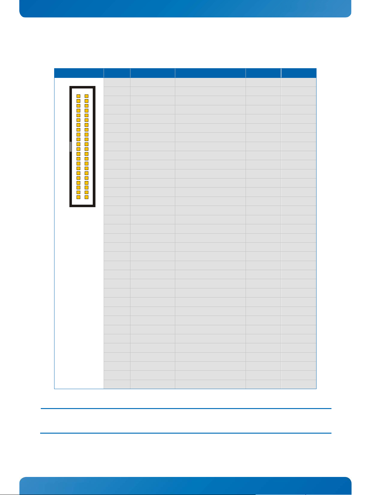
KTT30/mITX Users Guide
UART1 J3
UART3 J6
ccTalk J29
Fan J15
Power J17
Power J2
(External)
Recovery J37
Frontpanel J7
Touch J30
SATA J28
SPI J35
USB2
J24
USB3
HDMI
LAN
J8
LineIn
J11
LineOut
J10
Mic
J9
USB Client
LVDS J1
Feature J36
Modem J27
mPCIe/mSATA
J36
mPCIe J5
S/PDIF-In J31
S/PDIF-Out J26
Headphone J32
SDcard1 J20
SDcard2 J19
SIM socket J33
JTAG (only on EFT)
5 Connectors Location
(Internal)
J24
J18
J12
Page 17

KTD-N0857-A Page 14 Connector Signal Definitions
KTT30/mITX Users Guide
6 Connector Signal Definitions
The following sections provide pin definitions and detailed description of all onboard connectors.
The connector definitions follow the following notation:
Column Name Description
Pin
Signal
Type
Ioh/Iol
The abbreviation tbd is used for specifications which are not available yet or which are not sufficiently
specified by the component vendors.
Shows the pin numbers in the connector.
The mnemonic name of the signal at the current pin. The notation “#” states that the signal
is active low.
AI: Analogue Input
AO: Analogue Output
I: Digital Input
IO: Digital Input / Output
IOD: Input / Open Drain output
O: Digital Output
DSO: Differential Signaling Output with complementary signals on two paired wires
DSI: Differential Signaling Input with complementary signals on two paired wires
DSIO: Differential Signaling Input / Output (combined DSO and DSI)
PWR: PoWeR supply or ground reference pins
NC: Pin Not Connected
Additional notations:
-5.0 +5.0V signal voltage level, e.g. I-5.0
-3.3 +3.3V signal voltage level, e.g. O-3.3
-1.8 +1.8V signal voltage level, e.g. IO-1.8
Ioh: Typical current in mA flowing out of an output pin through a grounded load while the
output voltage has high level.
Iol: Typical current in mA flowing into an output pin from a VCC connected load while the
output voltage has low level.
Page 18

KTD-N0857-A Page 15 Rear Connectors
KTT30/mITX Users Guide
1
1
7 Rear IO Connectors
7.1 DC Power Connector
The KTT30/mITX board has a power input voltage range from +4.5V to +5.5V. All other voltages are generated onboard (e.g. +3.3V / +1.8V system voltage).
The power supply is supplied via the connector J2 (3 pins, DC power jacket 2.1mm).
Header Pin Signal Description
Alternative through the internal Power connector J17 (4 pin Micro-Fit). Notice that the +5V power lines on
J2 and on J17 are connected on the board.
1
2
3
VCC5 1)
GND
GND
Power supply +5V
Ground
Ground
Note: 1) To protect the external power lines of peripheral devices make sure that
- the wires have the right diameter to withstand the maximum available current.
- to enclosure of the peripheral device fulfills the fire-protecting conditions of IEC/EN 60950.
7.2 USB Connectors (Standard USB2.0)
The USB interface comes with three USB ports which follow the EHCI specification (USB 2.0 compliant). You
can expand the amount of USB connections by adding external hubs. Two ports are available on a standard
connector and one (client) port on a micro USB connector. All ports support USB 1.1 low and full speed
devices without a companion USB 1.1 host controller.
Two USB ports are available through the standard USB connectors J23 and J24.
Header Pin Signal Description Type
1
2
3
4
VCC5 1)
USB-
USB+
GND
Power +5V PWR
USB port (negative) DSIO-3.3
USB port (positive) DSIO-3.3
Ground PWR
Notes: 1) To protect the external power lines of peripheral devices make sure that
- the wires have the right diameter to withstand the maximum available current.
- to enclosure of the peripheral device fulfills the fire-protecting conditions of IEC/EN 60950.
The contacts for USB devices are protected and suitable to supply USB devices with a maximum input current of 500mA. Do
not supply external USB devices with higher power dissipation through these pins
Page 19

KTD-N0857-A Page 16 Rear Connectors
KTT30/mITX Users Guide
1
2
7.3 HDMI® Connector
Graphics Processing Unit
The graphics accelerator supports a HDMI® interface with Full HD resolution, a variety of LVDS LCD panels
with double clock, color depths of 18/24 bit and resolutions up to 1920 x 1200 pixels.
The HDMI
®
interface is available through the standard 19 pin Type A HDMI® connector J18.
Header Pin Signal Description Type
1
2
3
4
5
6
7
8
9
10
11
12
13
14
15
16
17
18
19
TMDS2+
GND
TMDS2-
TMDS1+
GND
TMDS1-
TMDS0+
GND
TMDS0-
TMDS_CLK+
GND
TMDS_CLK-
CEC
N.C.
DDC_CLK
DDC_DATA
GND
VCC5 1)
TMDS_HPD
TMDS data 2 (positive) DSO-3.3
Ground PWR
TMDS data 2 (negative) DSO-3.3
TMDS data 1 (positive) DSO-3.3
Ground PWR
TMDS data 1 (negative) DSO-3.3
TMDS data 0 (positive) DSO-3.3
Ground PWR
TMDS data 0 (negative) DSO-3.3
TMDS clock (positive) DSO-3.3
Ground PWR
TMDS clock (negative) DSO-3.3
Consumer Electronics Control IO-5.0
Not connected NC
DDC clock IO-5.0
DDC data IO-5.0
Ground PWR
Power +5V PWR
Hotplug detect I-5.0
Note: 1) To protect the external power lines of peripheral devices make sure that
- the wires have the right diameter to withstand the maximum available current.
- to enclosure of the peripheral device fulfills the fire-protecting conditions of IEC/EN 60950.
Page 20

KTD-N0857-A Page 17 Rear Connectors
KTT30/mITX Users Guide
1
7.4 LAN Connector
The KTT30 uses an Intel® 82574 Gigabit PCI Express® LAN controller which supports 10/100/1000 Base-T
interfaces. The controller auto-negotiates the management of a 10, 100 or 1000 Mbps connection. Additionally you can boot up the board via a network connection from a PXE server.
The LAN interface is available through the standard RJ45 connector J8 (8 pins).
Header Pin Signal Description Type
1
2
3
4
5
6
7
8
TXD+ / MDIO1+
TXD- / MDIO1-
RXD+ / MDIO2+
MDIO3+
MDIO3-
RXD- / MDIO2-
MDIO4+
MDIO4-
10/100 transmit / 1000 pair 1 (positive) DSO / DSIO
10/100 transmit / 1000 pair 1 (negative) DSO / DSIO
10/100 receive / 1000 pair 2 (positive) DSI / DSIO
1000 pair 3 (positive) DSIO
1000 pair 3 (negative) DSIO
10/100 receive / 1000 pair 2 (negative) DSI / DSIO
1000 pair 4 (positive) DSIO
1000 pair 4 (negative) DSIO
7.5 Audio Interface
The SoC supports an Inter-IC Sound (I2S) codec with 24 bit resolution and 96 kHz sample rate (the
maximum rate of 96 kHz only unidirectional). The analogue-to-digital part of the codec uses 24 bit, 128x
oversampled sigma-delta ADCs. The digital-to-analogue part contains two 24 bit sigma-delta DACs. The
interface includes LINE OUT, LINE IN, MICROPHONE IN and a digital S/PDIF output.
Output resolution (LINE OUT, S/PDIF) 16/20/24 bit
Output sample rate (LINE OUT, S/PDIF) 44.1/48/96 kHz
Output signal-to-noise ratio (LINE OUT) 96 dB
Input signal-to-noise ratio (LINE IN) 92 dB
Parameter Values Units
Input resolution (LINE IN) 16/20/24 bit
Input sample rate (LINE IN) 44.1/48/96 kHz
7.6 Analog Connectors
The analog audio interface uses three TRS (Tip, Ring, Sleeve) connectors J9 to J11 (3 pins).
Header Pin J11
BLUE
Tip
Ring
Sleeve
LINEIN-L LINEOUT-L MIC-L
LINEIN-R LINEOUT-R MIC-R
GND GND GND
J10
LIME
J9
PINK
Type
IA resp. OA (J10)
IA resp. OA (J10)
PWR
Page 21

KTD-N0857-A Page 18 Rear Connectors
KTT30/mITX Users Guide
1
7.7 Micro USB Connector
The connector J12 (5 pins) provides the USB Client functionality (default setting).
You need the client functionality for changing the bootloader or update a corrupted bootloader. Together
with the recovery pin (see chapter “Debug/Design Tools”) and dedicated software on a desktop computer
as well as a standard USB cable the upload.
Header Pin Signal Description Type
1
2
3
4
5
VCC5 1)
USB-
USB+
ID
GND
Power +5V PWR
USB port (negative) DSIO-3.3
USB port (positive) DSIO-3.3
Host / slave detection
(grounded or opened)
Ground PWR
I
Notes: 1) To protect the external power lines of peripheral devices make sure that
- the wires have the right diameter to withstand the maximum available current.
- to enclosure of the peripheral device fulfills the fire-protecting conditions of IEC/EN 60950.
The contacts for USB devices are protected and suitable to supply USB devices with a maximum input current of 500mA. Do
not supply external USB devices with higher power dissipation through these pins
Page 22

KTD-N0857-A Page 19 Pin Connectors
KTT30/mITX Users Guide
8 Pin Connectors
8.1 LVDS Flat Panel Connector
The J1 connector (40 pins) provides the LVDS interface for flat panels on the top side of the board.
Header Pin Signal Description Type
1 - 5
6
7
8
9 - 10
11
12
13
14
15
16
17
18
19
20
21
22
23
24
25
26
27 - 28
29
30
31
32
33
34
35
36
37
38
39 - 40
VCC5 1)
GND
VCC5 1)
GND
LCDVCC 1)
DDC_CLK
DDC_DATA
BKLTADJ
VCCENABLE
BKLTON
GND
LVDSA0-
LVDSA0+
LVDSA1-
LVDSA1+
LVDSA2-
LVDSA2+
LVDSAC-
LVDSAC+
LVDSA3-
LVDSA3+
GND
LVDSB0-
LVDSB0+
LVDSB1-
LVDSB1+
LVDSB2-
LVDSB2+
LVDSBC-
LVDSBC+
LVDSB3-
LVDSB3+
GND
First channel data 0 output (negative) DSO-3.3
First channel data 0 output (positive) DSO-3.3
First channel data 1 output (negative) DSO-3.3
First channel data 1 output (positive) DSO-3.3
First channel data 2 output (negative) DSO-3.3
First channel data 2 output (positive) DSO-3.3
First channel clock output (negative) DSO-3.3
First channel clock output (positive) DSO-3.3
First channel data 3 output (negative) DSO-3.3
First channel data 3 output (positive) DSO-3.3
Second channel data 0 output (negative) DSO-3.3
Second channel data 0 output (positive) DSO-3.3
Second channel data 1 output (negative) DSO-3.3
Second channel data 1 output (positive) DSO-3.3
Second channel data 2 output (negative) DSO-3.3
Second channel data 2 output (positive) DSO-3.3
Second channel clock output (negative) DSO-3.3
Second channel clock output (positive) DSO-3.3
Second channel data 3 output (negative) DSO-3.3
Second channel data 3 output (positive) DSO-3.3
Power +5V PWR
Ground PWR
Power +5V PWR
Ground PWR
Panel power +3.3V or +5V PWR
DDC clock IO-3.3
DDC data IO-3.3
Brightness control PWM-3.3
Panel power enable O-3.3
Backlight on/off O-3.3
Ground PWR
Ground PWR
Ground PWR
Page 23

KTD-N0857-A Page 20 Pin Connectors
KTT30/mITX Users Guide
!
Warning
connector Fan might be damaged.
Note: The backlight adjust signal uses the Pulse Width Modulation (PWM) technique. A proto- type cable
with open ends is shippable from KONTRON (part number 821515).
Note: 1) To protect the external power lines of peripheral devices make sure that
- the wires have the right diameter to withstand the maximum available current.
- to enclosure of the peripheral device fulfills the fire-protecting conditions of IEC/EN 60950.
Warning: Check the U-Boot Setup for correct settings for your panel – not doing so might cause permanent damage to your panel.
Connecting a Flat Panel
Check if you have the correct panel cable. Inspect the cable for damages.
Switch on the power supply and activate/save the desired settings with help of the U-Boot
bootloader (for further details see the 'Software Guide' chapter 'U-Boot Setup'). Switch off
the power supply.
Connect an external power supply for the correct backlight voltage (except the power supply
complies with the backlight voltage).
Connect the cable to the flat panel connector J1 on the KTT30 and connect the other end to
your display.
Switch on the power supply. If you only see a blank screen contact your distributor for tech-
nical support.
8.2 Fan Connector
For an optional fan use the connector J15 (4 pins). The interface only supports +5V fans and operates with
a PWM output (Control) which allows the control of fan speed.
Note: 1) To protect the external power lines of peripheral devices make sure that
- the wires have the right diameter to withstand the maximum available current.
- to enclosure of the peripheral device fulfills the fire-protecting conditions of IEC/EN 60950.
Header Pin Signal Description Type
: Do not mix the Fan Connector and the ccTalk connector. If mounting Fan into ccTalk
1
2
3
4
Control
Sence
VCC5 1)
GND
PWM output O-5.0
Tacho signal (open drain) I
Power +5V PWR
Ground PWR
Page 24

KTD-N0857-A Page 21 Pin Connectors
KTT30/mITX Users Guide
!
Warning
1
8.3 COM ports (RS232)
Two serial ports provide asynchronous serial communication with RS-232 interfaces. They are 16450/
16550 UART compatible and support 16-byte FIFO buffers for transfer rates from 50 Baud to 115.2 kBaud.
UARTC/UART3 can be configured as a standard serial or as a ccTalk interface. With a solder jumper it is
possible to activate the ccTalk interface, often used in automatic payment equipment.
Connector assignment:
J3 UARTA/UART1
J6 UARTC/UART3
The serial ports are available through the connectors J3 and J6 (10 pins).
Header Pin Signal J3 J6 Description Type
1
2
3
4
5
6
7
8
9
10
DCD#
DSR#
RXD
RTS#
TXD
CTS#
DTR#
RI#
GND
VCC5 1) 2)
Data carrier detect I
Data set ready I
Receive serial data I
Request to send O
Transmit serial data O
Clear to send I
Data terminal ready O
Ring indicator I
Ground PWR
Power +5V PWR
8.4 ccTalk Connector
The ccTalk interface uses the fan connector J29 (4 pins).
Header Pin Signal Description Type
Notes: 1) To protect the external power lines of peripheral devices make sure that
- the wires have the right diameter to withstand the maximum available current.
- to enclosure of the peripheral device fulfills the fire-protecting conditions of IEC/EN 60950.
2) The +5V supply voltage is protected with a common 1.5A resetable fuse.
Connector then ccTalk device and or mother board might be damaged.
: Do not mix the ccTalk Connector with the Fan Connector. If mounting ccTalk device into Fan
1
2
3
4
VCC5 1)
N.C.
GND
DATA
Power +5V PWR
Not connected NC
Ground PWR
Serial data line (RXD/TXD) IO
Page 25

KTD-N0857-A Page 22 Pin Connectors
KTT30/mITX Users Guide
1
8.5 Serial Console
Most operating systems have a defined serial console. The KTT30/mITX board uses the first serial port
(UARTA/ UART1) on connector J3 for this purpose. Normally the serial console needs only three signal lines
(TXD, RXD and GND). The serial port is assigned to the environment variables stdin, stdout and stderr. If
you use U-Boot as bootloader you can interact with U-Boot via a USB keyboard and a standard terminal
program on a desktop computer. The following overview shows the default serial settings:
Baudrate 115 kBaud
Data bits 8
Stop bits 1
Parity No
8.6 Digital Connectors (S/PDIF)
The digital audio interface is available through the connectors J26 and J31 (2 pins).
Header Pin J26 J31 Type
1
2
SPDIF_OUT SPDIF_IN
GND GND
O resp. I (J31)-3.3
PWR
8.7 Headphone Connector
The headphone interface is available through the connector J32 (4 pins).
Header Pin Signal Type
1
2
3
4
GND
HPOUT-L
GND
HPOUT-R
PWR
AO
PWR
AO
Page 26

KTD-N0857-A Page 23 Pin Connectors
KTT30/mITX Users Guide
1
8.8 Front Panel Header (FRONTPNL)
The power button and other power signals are available through the pin header J7 (16 pins).
Header Pin Signal Description Type Ioh/Iol
1
2
3
4
5
6
7
8
9
10
11
12
13
14
15
16
GND
GND
BKLTADJ_DWN
BKLTADJ_UP
VCC5 1)
VCC5 1)
SATA_LED+
DEEP_SLEEP
GND
PWR_BTN+ 2)
RESET_IN
PWR_BTN-
VCC3 1)
GND
GND
GND
Ground
Ground
Backlight brightness down
Backlight brightness up
Power supply +5V
Power supply +5V
S-ATA® LED
Indicates deep sleep mode
Ground
Power button (positive)
Board reset input
Power button (negative) = GND
Power supply +3.3V
Ground
Ground
Ground
PWR
PWR
I-1.8
I-1.8
PWR
PWR
O-3.3
O-5.0
PWR
I-5.0
I
PWR
PWR
PWR
PWR
PWR
Notes: 1) To protect the external power lines of peripheral devices make sure that
- the wires have the right diameter to withstand the maximum available current.
- to enclosure of the peripheral device fulfills the fire-protecting conditions of IEC/EN 60950.
2) The label PWR_BTN (power button) is identical with NVIDIAs® 'ONKEY' button.
Page 27
KTD-N0857-A Page 24 Pin Connectors
KTT30/mITX Users Guide
Header
Pin
Signal
Description
Type
Ioh/Iol
N.C.
EXT_BAT
VCC5 1)
GPIO2
GPIO6
GPIO8
GPIO11
GPIO15
GND
N.C.
1
8.9 Feature Connector
The General Purpose I/O ‘s and a few other signals are available through the Feature connector J36.
1 CASE_OPEN# Case opened detection I
2
3 CORE_PWR_ON T30 core rail enabled O-5.0
4
5 DEEP_SLEEP Indicates deep sleep mode O-5.0
6
7 - 8 N.C. Not connected NC
9
10
11
12 GPIO1 General purpose I/O 1 IO-3.3
13
14 GPIO3 General purpose I/O 3 IO-3.3
15
16 GPIO5 General purpose I/O 5 IO-3.3
17
18 GPIO7 General purpose I/O 7 IO-3.3
19 - 20
21
22
23 GPIO10 General purpose I/O 10 IO-3.3
24
25 GPIO12 General purpose I/O 12 IO-3.3
26
27 GPIO14 General purpose I/O 14 IO-3.3
28
29 GPIO16 General purpose I/O 16 IO-3.3
30
31 - 32
33 - 37
38 GND Ground PWR
39 - 40
41 - 43 GND Ground PWR
44
N.C.
VCC3 1)
GPIO0
GPIO4
GND
GPIO9
GPIO13
GPIO17
N.C.
CPU_PWR_ON
Not connected NC
Not connected NC
External battery input PWR
Power +3.3V PWR
Power +5V PWR
General purpose I/O 0 IO-3.3
General purpose I/O 2 IO-3.3
General purpose I/O 4 IO-3.3
General purpose I/O 6 IO-3.3
Ground PWR
General purpose I/O 8 IO-3.3
General purpose I/O 9 IO-3.3
General purpose I/O 11 IO-3.3
General purpose I/O 13 IO-3.3
General purpose I/O 15 IO-3.3
General purpose I/O 17 IO-3.3
Ground PWR
Not connected NC
Not connected NC
T30 CPU rail enabled O-5.0
Note: 1) To protect the external power lines of peripheral devices make sure that
- the wires have the right diameter to withstand the maximum available current.
- to enclosure of the peripheral device fulfills the fire-protecting conditions of IEC/EN 60950.
Page 28

KTD-N0857-A Page 25 Pin Connectors
KTT30/mITX Users Guide
that the T30 CPU rail has been enabled. The signal is
The General Purpose I/O‘s and a few other signals are available through the Feature connector J36.
Signal Description
CASE_OPEN#
CORE_PWR_ON
DEEP_SLEEP
EXT_BAT
CPU_PWR_ON
The three signals for LED usage assume the following states during power management:
This signal is used to detect if the system case has been opened.
This signal is an active high indication that the T30 CORE rail has been enabled. The signal is
buffered for LED usage.
This signal is an active high indication that the system has entered the deep sleep mode. The
signal is buffered for LED usage.
EXTernal BATtery option for connecting the plus pin or terminal of an external primary cell battery
(2.5 to 4.0V). The minus pin or terminal should be connected to a GND pin. The external battery is
protected against charging and can be used with or without the onboard battery installed.
This signal is an active high indication
buffered for LED usage.
Signal ACTIVE SUSPEND DEEP SLEEP
CORE_PWR_ON
CPU_PWR_ON
DEEP_SLEEP
High High Low
High Low Low
Low Low High
General Purpose I/O Interface
The General Purpose I/O interface is a subset of a multifunction part from NVIDIAs® Tegra® 3 SoC. All I/O
pins have additional functionalities which can be changed by software.
The I/O signals are decoupled to 3.3V voltage level by voltage level translators. With one I/O line (NVIDIA
label: Q.00) you can enable or disable all voltage level translators:
Active state high level
Tri-state low level
Electrical Specifications
Digital Input Min. Typ. Max. Units
Input LOW voltage +1.1 V
Input HIGH voltage +2.2 3.3 +3.8 V
Input rate (Linux) tbd. kHz
®
Digital Outputr Min. Typ. Max. Units
Output LOW voltage +0.4 V
Output HIGH voltage +2.9 +3.3 V
Continuous output current per pin 8 mA
Switching rate (Linux) tbd. kHz
Page 29

KTD-N0857-A Page 26 Pin Connectors
KTT30/mITX Users Guide
I/O Pin
NVIDIA® Label
Second Function
GPIO2
GPIO5
GPIO9
GPIO12
GPIO15
Header
Pin
Signal
Description
GND
Multifunction Overview
The following table informs about the dependencies.
GPIO0
GPIO1
GPIO3
GPIO4
GPIO6
GPIO7
GPIO8
GPIO10
GPIO11
GPIO13
GPIO14
GPIO16
GPIO17
Q.01
Q.02
Q.03
Q.04
Q.05
Q.06
Q.07
R.00
R.01
R.02
R.03
R.04
R.05
S.01
S.02
S.03
S.04
S.05
8.10 DC Power Connector Internal
Keyboard column 1
Keyboard column 2
Keyboard column 3
Keyboard column 4
Keyboard column 5
Keyboard column 6
Keyboard column 7
Keyboard row 0
Keyboard row 1
Keyboard row 2
Keyboard row 3
Keyboard row 4
Keyboard row 5
Keyboard row 9
Keyboard row 10
Keyboard row 11
Keyboard row 12
Keyboard row 13
The KTT30/mITX board has a power input voltage range from +4.5V to +5.5V. The power supply is connected
via the connector J17 (4 pin Micro-Fit) or alternatively the external Power connector J2 (3 pins, DC power
jacket 2.1mm). Notice that the +5V power lines on J2 and on J17 are connected on the board.
1
2
3
4
VCC5 1)
GND
VCC5 1)
Power supply +5V
Ground
Ground
Power supply +5V
Warning: Do not overload the onboard system voltage +3.3V resp. 1.8V (SDTM card socket, digital I/O connector). The maximum
current should not exceed 250mA.
Note: 1) To protect the external power lines of peripheral devices make sure that
- the wires have the right diameter to withstand the maximum available current.
- to enclosure of the peripheral device fulfills the fire-protecting conditions of IEC/EN 60950.
Page 30

KTD-N0857-A Page 27 Pin Connectors
KTT30/mITX Users Guide
1
8.11 Touch Interface
By default the touch screen interface supports an I2CTM connection. Alternative a stuffing option allows the
usage of a standard SPI
The touch screen interface is available through the connector J30 (12 pins).
Header Pin Signal Description Type
TM
port. The complete interface is 3.3V compatible.
1
2
3
4
5
6
7
8
9
10
11
12
AVCC3 1)
AVCC3 1)
AVCC3 1)
VCC3 1)
SPI_CLK
SPI_CS#
TS_IRQ#
I2C_SDA
SPI_MOSI
I2C_SCL
SPI_MISO
TS_RST#
GND
VCC1 1)
SPITM clock (alternative) O-3.3
SPITM slave select (alternative) O-3.3
SPITM master output (alternative)
SPITM master input (alternative)
Analog power +3.3V PWR
Analog power +3.3V PWR
Analog power +3.3V PWR
Digital power +3.3V PWR
Interrupt (optional) I-3.3
I2CTM data
I2CTM clock
Reset (optional) O-3.3
Ground PWR
Digital power +1.8V PWR
IO-3.3
O-3.3
IO-3.3
I-3.3
Note: 1) To protect the external power lines of peripheral devices make sure that
- the wires have the right diameter to withstand the maximum available current.
- to enclosure of the peripheral device fulfills the fire-protecting conditions of IEC/EN 60950.
Page 31

KTD-N0857-A Page 28 Pin Connectors
KTT30/mITX Users Guide
1
2
9
10
8.12 SPITM Interface
The KTT30 provides one synchronous full duplex Serial Peripheral Interface Bus (SPITM) for customer requirements. All four SPITM signals are 5V tolerant.
Two things should be considered:
1. An onboard SPITM flash coexists on the same interface lines. You must disable this component with a
3.3V power connection to the ADDIN signal (e.g. a short circuit jumper between pin 2 and 4).
TM
2. The four SPI
output enable pin. For normal operation this signal should be high.
The SPI
TM
interface is available on connector J35 (pin header, 10 pins).
lines are protected with an additional bus driver and the ISOLATE# signal controls the
Header Pin Signal Description Type
1
2
3
4
5
6
7
8
9
10
SPI_CLK
VCC3 1)
SPI_CS#
ADDIN
RSVD
N.C.
SPI_MOSI
ISOLATE#
SPI_MISO
GND
SPITM clock O-3.3
Power +3.3V PWR
SPITM slave select O-3.3
Disable onboard SPI flash I-3.3
Reserved (10k pullup to 3.3V) PWR
Not connected NC
SPITM master output O-3.3
Disable the SPI interface I-3.3
SPITM master input I-3.3
Ground PWR
CAUTION!
If you permanently disable the onboard SPITM flash then you disable the
standard boot device which contains the U-Boot bootloader. In this case
please contact your local Distributor or Field Application Engineer (FAE).
Note: 1) To protect the external power lines of peripheral devices make sure that
- the wires have the right diameter to withstand the maximum available current.
- to enclosure of the peripheral device fulfills the fire-protecting conditions of IEC/EN 60950.
Page 32

KTD-N0857-A Page 29 Slot Connectors
KTT30/mITX Users Guide
9
1
8
1
9 Standard Slot Connectors
9.1 SATA Connector
Only one S-ATA® 2.0 port is available. Serial-ATA® connections boost the data rate theoretically up to 300
MB/sec. In addition it changes the parallel interface requiring 40 separate wires to a serial interface requiring only 6 wires. The controller supports the Advanced Host Controller Interface (AHCI).
Note that SATA connector shares the internal SATA port with mSATA connector. If mSATA card is plugged in,
then hardware automatically switches from the SATA connector to the mSATA card socket.
The S-ATA® interface is available through the standard L-type connector J28 (7 pins).
Header Pin Signal Description Type
1
2
3
4
5
6
7
GND
TX+
TX-
GND
RXRX+
GND
Ground PWR
Transmit (positive) DSO
Transmit (negative) DSO
Ground PWR
Receive (negative) DSI
Receive (positive) DSI
Ground PWR
9.2 Secure Digital and Multimedia Card
The SD/MMC interface uses two standard SDTM card sockets as well as an onboard SanDisk® 16 GByte
TM
embedded flash drive with an e.MMC interface. The controller supports the SD
(implies the SDSC, SDHC and SDXC families) and the MMC specification revision 4.4. The data bus width
accounts 4 bits for the standard sockets and 8 bits for the flash drive, the SDTM card transfer rate can be up
to 50 MHz and MMC rate up to 52 MHz. The onboard SanDisk
®
16 GByte embedded flash drive is bootable.
The SDTM card sockets are named J19 and J20 (9 pins).
Header Pin Signal Description Type
1
2
3
4
5
6
7
8
9
CD / DATA3
CMD
GND
VCC3 1)
CLK
GND
DATA0
DATA1
DATA2
Card detect / Data bit 3 IO-3.3
Command line IO-3.3
Ground PWR
Power +3.3V PWR
Clock O-3.3
Ground PWR
Data bit 0 IO-3.3
Data bit 1 IO-3.3
Data bit 2 IO-3.3
specification revision 3.0
Page 33

KTD-N0857-A Page 30 Slot Connectors
KTT30/mITX Users Guide
1
9.3 Mini PCI Express® Connector
NVIDIAs® Tegra® 3 supports the PCI Express® specification 1.1 with 2.5 GT/s (GigaTransfers/s - identical
with Gigabits/s by one lane). Two ports with one lane are provided for free usage. The first port has no
®
additional features, the second port allows the switching between mini PCI Express
®
The pure mini PCI Express
port is available through the connector J5 (52 pins).
Header Pin Signal Description Type Pin Signal Description Type
1
3
5
7
9
11
13
15
17
19
21
23
25
27
29
31
33
35
37
39
41
43
45
47
49
51
WAKE#
N.C.
N.C.
CLKREQ#
GND
PE_CLK-
PE_CLK+
GND
N.C.
N.C.
GND
PE_RX-
PE_RX+
GND
GND
PE_TX-
PE_TX+
GND
GND
VCC3 1)
VCC3 1)
GND
N.C.
N.C.
N.C.
N.C.
Wake event I-3.3 2
Not connected NC 4
Not connected NC 6
PCIe® clock request I-3.3 8
Ground PWR 10
PCIe® clock (neg.) DSO 12
PCIe® clock (pos.) DSO 14
Ground PWR 16
Not connected NC 18
Not connected NC 20
Ground PWR 22
PCIe® receive (neg.) DSI 24
PCIe® receive (pos.) DSI 26
Ground PWR 28
Ground PWR 30
PCIe® transmit (neg.) DSO 32
PCIe® transmit (pos.) DSO 34
Ground PWR 36
Ground PWR 38
Power +3.3V PWR 40
Power +3.3V PWR 42
Ground PWR 44
Not connected NC 46
Not connected NC 48
Not connected NC 50
Not connected NC 52
VCC3 1)
GND
VCC1 1)
N.C.
N.C.
N.C.
N.C.
N.C.
GND
W_DISABLE#
PE_RST#
VCC3 1)
GND
VCC1 1)
I2C_CLK
I2C_DATA
GND
N.C.
N.C.
GND
N.C.
N.C.
N.C.
VCC1 1)
GND
VCC3 1)
and mini S-ATA®.
Power +3.3V PWR
Ground PWR
Power +1.5V PWR
Not connected NC
Not connected NC
Not connected NC
Not connected NC
Not connected NC
Ground PWR
Wireless disable O-3.3
PCIe® reset O-3.3
Power +3.3V PWR
Ground PWR
Power +1.5V PWR
I2CTM clock O-3.3
I2CTM data IO-3.3
Ground PWR
Not connected NC
Not connected NC
Ground PWR
Not connected NC
Not connected NC
Not connected NC
Power +1.5V PWR
Ground PWR
Power +3.3V PWR
Page 34

KTD-N0857-A Page 31 Slot Connectors
KTT30/mITX Users Guide
1
9.4 m PCIe / mSATA Connector
The mPCIe / mSATA port is available through the connector J4 (52 pins).
Header
Pi
11
13
15
17
19
21
23
25
27
29
31
33
35
37
39
41
43
45
47
49
51
Signal Description Type Pin Signal Description Type
n
WAKE#
1
3
5
7
9
N.C.
N.C.
CLKREQ#
GND
PE_CLK-
PE_CLK+
GND
N.C.
N.C.
GND
PE_RX-
SATA_RX+
PE_RX+
SATA_RX-
GND
GND
PE_TX-
SATA_TX-
PE_TX+
SATA_TX+
GND
GND
VCC3 1)
VCC3 1)
GND
N.C.
N.C.
N.C.
SEL_SATA#
Wake event I-3.3 2
Not connected NC 4
Not connected NC 6
PCIe® clock request I-3.3 8
Ground PWR 10
PCIe® clock (neg.) DSO 12
PCIe® clock (pos.) DSO 14
Ground PWR 16
Not connected NC 18
Not connected NC 20
Ground PWR 22
PCIe® receive (neg.)
S-ATA® receive (pos.)
PCIe® receive (pos.)
S-ATA® receive (neg.)
Ground PWR 28
Ground PWR 30
PCIe® transmit (neg.)
S-ATA® transmit (neg.)
PCIe® transmit (pos.)
S-ATA® transmit (pos.)
Ground PWR 36
Ground PWR 38
Power +3.3V PWR 40
Power +3.3V PWR 42
Ground PWR 44
Not connected NC 46
Not connected NC 48
Not connected NC 50
S-ATA® identification I-1.8 52
DSI 24
DSI 26
DSO 32
DSO 34
VCC3 1)
GND
VCC1 1)
N.C.
N.C.
N.C.
N.C.
N.C.
GND
W_DISABLE#
PE_RST#
VCC3 1)
GND
VCC1 1)
I2C_CLK
I2C_DATA
GND
N.C.
N.C.
GND
N.C.
N.C.
N.C.
VCC1 1)
GND
VCC3 1)
Power +3.3V PWR
Ground PWR
Power +1.5V PWR
Not connected NC
Not connected NC
Not connected NC
Not connected NC
Not connected NC
Ground PWR
Wireless disable O-3.3
PCIe® reset O-3.3
Power +3.3V PWR
Ground PWR
Power +1.5V PWR
I2CTM clock IO-3.3
I2CTM data IO-3.3
Ground PWR
Not connected NC
Not connected NC
Ground PWR
Not connected NC
Not connected NC
Not connected NC
Power +1.5V PWR
Ground PWR
Power +3.3V PWR
Note that SATA connector shares the internal SATA port with mSATA connector. If mSATA card is plugged in,
then hardware automatically switches from the SATA connector to the mSATA card socket.
Page 35

KTD-N0857-A Page 32 Slot Connectors
KTT30/mITX Users Guide
1
9.5 Modem Card Connector
The second host port (named USB2) can also be configured as a miniPCI Express® USB modem interface.
With an USB 2.0 switch the host port supports either the standard connector J24 or the USB modem
interface on connector J27. One I/O line (NVIDIA® label: L.05) enables the switching between the
interfaces:
Standard connector J24 low level
Modem card connector J27 high level
The modem card interface is available through the connector J27 (52 pins).
Header Pin Signal Description Type Pin Signal Description Type
1
3
5
7
9
11
13
15
17
19
21
23
25
27
29
31
33
35
37
39
41
43
45
47
49
51
WAKE#
N.C.
N.C.
N.C.
GND
N.C.
N.C.
GND
USIM_USB-
USIM_USB+
GND
N.C.
N.C.
GND
GND
N.C.
N.C.
GND
GND
VCC3 1)
VCC3 1)
GND
MODEM_CLK
MODEM_DIN
MODEM_DOUT
MODEM_CS
Wake event I-3.3 2
Not connected NC 4
Not connected NC 6
Not connected NC 8
Ground PWR 10
Not connected NC 12
Not connected NC 14
Ground PWR 16
USIM USB (neg.) DSIO 18
USIM USB (pos.) DSIO 20
Ground PWR 22
Not connected NC 24
Not connected NC 26
Ground PWR 28
Ground PWR 30
Not connected NC 32
Not connected NC 34
Ground PWR 36
Ground PWR 38
Power +3.3V PWR 40
Power +3.3V PWR 42
Ground PWR 44
Modem clock O 46
Modem data in O 48
Modem data out I 50
Modem chip sel. O 52
VCC3 1)
GND
VCC1 1)
USIM_VCC
USIM_IO
USIM_CLK
USIM_RST
USIM_VPP
GND
W_DISABLE#
PE_RST#
VCC3 1)
GND
VCC1 1)
I2C_CLK
I2C_DATA
GND
USB-
USB+
GND
N.C.
N.C.
N.C.
VCC1 1)
GND
VCC3 1)
Power +3.3V PWR
Ground PWR
Power +1.5V PWR
USIM power PWR
USIM data IO
USIM clock O
USIM reset O
USIM progr. volt. PWR
Ground PWR
Wireless disable O-3.3
PCIe® reset O-3.3
Power +3.3V PWR
Ground PWR
Power +1.5V PWR
I2CTM clock O-3.3
I2CTM data IO-3.3
Ground PWR
USB port (neg.) DSIO
USB port (pos.) DSIO
Ground PWR
Not connected NC
Not connected NC
Not connected NC
Power +1.5V PWR
Ground PWR
Power +3.3V PWR
Page 36

KTD-N0857-A Page 33 Appendix
KTT30/mITX Users Guide
Appendix A: System Resources
A.1 Memory Area
All registers of the Tegra® 3 processor are memory-mapped. Do not write to the register range if you have
no knowledge about the register function.
Memory Range Used for Available Comment
00000000h - 3FFFFFFFh
40000000h - 4003FFFFh
50000000h - 7FFFFFFFh
80000000h - FFEFFFFFh
PCI Express® memory No Reserved for operating systems
Internal RAM (IRAM) No Normally do not access the IRAM
Processor registers No
External SDRAM Yes Read- and writeable
Page 37

KTD-N0857-A Page 34 Appendix
KTT30/mITX Users Guide
(External)
PN
Qty.
Description
821017
2
Cable, COM, 2.54mm, 100mm
821515
1
Cable, LVDS Open-End
821035
1
Cable, SATA, 500mm
1052-5885
1
Cable, Feature 44pol 1 to1, 300mm
1055-5493
1
Cable, Front Panel 16pol, Open-End
1052-5080
1
Cable ATX Power for KTT30
Appendix B: Mating Connectors
The Mating connectors / Cables are connectors or cable kits which are fitting the On-board connector.
Connector
Onboard Connectors Mating Connectors
Manufacturer P/N Manufacturer P/N
Power
Power
(Internal)
LVDS J1
Fan J15
ccTalk J29
UART1/UART3 J3/J6
Frontpanel J7
Touch J30 MOLEX 54550-1294
Feature J36
S/PDIF-In J31
S/PDIF-Out J26
Headphone J32
J2 Kycon KLDHCX-0202-A-LT
J17
Molex 0430450402 MOLEX 43025-0400
Kontron KT 1052-5080 (cable kit)
SAMTEC SHF-120-01-F-D-SM-K-TR
Hon Kon Technology HB12-220-VFS-20R
WIESON TECHNOLOGIES G2124-03200101-00
DON CONNEX C44-40BSBC1-G
MOLEX 22-05-3041 MOLEX 22-01-2045
FOXCONN HF1804E-K
MOLEX 22-05-3041 MOLEX 22-01-2045
FOXCONN HF1804E-K
PINREX 511-90-10GB00
FOXCONN HL8605V
PINREX 511-90-16GB00
FOXCONN HL8608V
PINREX 52C-90-44GB00
FOXCONN HS5422F
MOLEX
MOLEX
MOLEX
53047-0210
53047-0210
53047-0410
Don Connex A32-40-C-G-B-1
Kontron KT 910000005
Kontron KT 821515 (cable kit)
Kontron KT 821155 (cable kit)
Molex 90635-1103
Kontron KT 821016 (cable kit)
Kontron KT 821017 (cable kit)
Molex 90635-1243
Kontron KT 1055-5493 (cable kit)
Don Connex A05c-44-B-G-A-1-G
MOLEX
MOLEX
MOLEX
KTT30 Cable kit PN 826604:
51021-0200
51021-0200
51021-0400
Page 38

KTD-N0857-A Page 35 Appendix
KTT30/mITX Users Guide
Appendix C: Reference Documents
KONTRON Technology A/S can't guarantee the availability of internet addresses.
Document Internet Address
NVIDIA® Development http://developer.nvidia.com/tools/Development
Linux® for Tegra® http://developer.nvidia.com/linux-tegra
Digital Visual Interface (DVI®) http://www.ddwg.org
Open LVDS Display Interface Standard Spec. (Open LDITM) http://www.national.com/analog/displays/open_ldi
IEEE 802.3® Specification (Ethernet) http://standards.ieee.org/getieee802
Universal Serial Bus Specification (USB) http://www.usb.org/developers/docs
PCI Express® Base Specification (PCI Express®) http://www.pcisig.com/specifications
High Speed Serialized AT Attachment (S-ATA) ® http://www.sata-io.org/developers
SD Specification (SD Card) http://www.sdcard.org/developers/tech/sdio/sdio_spec
Corporate Offices
Europe, Middle East & Africa
Oskar-von-Miller-Str. 1
85386 Eching/Munich
Germany
Tel.: +49 (0) 8165/ 77 777
Fax: +49 (0) 8165/ 77 219
info@kontron.com
North America
14118 Stowe Drive
Poway, CA 92064-7147
USA
Tel.: +1 888 294 4558
Fax: +1 858 677 0898
info@us.kontron.com
Asia Pacific
17 Building,Block #1,ABP
188 Southern West 4th Ring Road
Beijing 100070, P.R.China
Tel.: + 86 10 63751188
Fax: + 86 10 83682438
info@kontron.cn
 Loading...