

Page 1
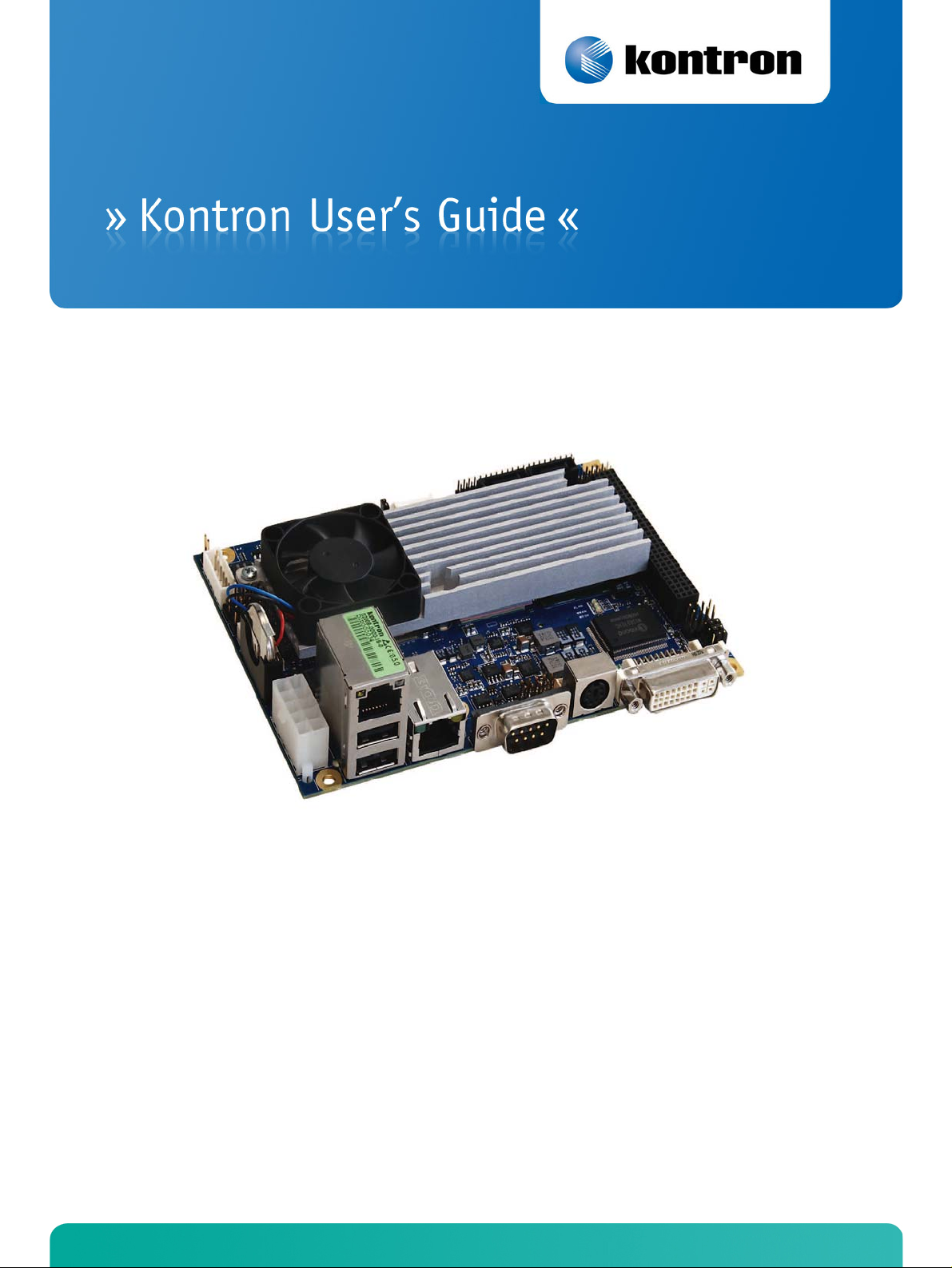
JRexplus-DC
KTD-S0008-F
Page 2

User Information
Table of Contents
» Table of Contents «
1 User Information .............................................................................1
1.1 About This Document.................................................................................................... 1
1.2 Copyright Notice.......................................................................................................... 1
1.3 Trademarks................................................................................................................. 1
1.4 Standards................................................................................................................... 1
1.5 Warranty .................................................................................................................... 1
1.6 Life Support Policy ....................................................................................................... 2
1.7 Technical Support ........................................................................................................ 2
2 Introduction ...................................................................................3
2.1 JRex Embedded Line Family ........................................................................................... 3
2.2 JRexplus-DC Overview ................................................................................................... 3
3 Specifications .................................................................................4
3.1 Functional Specifications .............................................................................................. 4
3.2 Block Diagram............................................................................................................. 7
3.3 Mechanical Specifications.............................................................................................. 8
3.4 Electrical Specifications ................................................................................................ 8
3.5 Real-Time Clock Battery................................................................................................. 9
3.6 Environmental Specifications ........................................................................................10
3.7 MTBF ........................................................................................................................10
4 Getting Started.............................................................................. 11
5 System Memory ............................................................................. 12
6 PCI Bus Expansion.......................................................................... 12
7 Graphics Interface.......................................................................... 13
7.1 DVI or CRT Connector ...................................................................................................13
7.2 DDC Interpretation......................................................................................................14
7.2.1 Jumper Setting ....................................................................................................................... 14
7.3 Flat Panel Connector....................................................................................................14
7.3.1 JILI30 Connector..................................................................................................................... 15
7.4 Panel Power...............................................................................................................16
7.5 Connecting a Flat Panel................................................................................................17
7.6 Available Video Modes .................................................................................................17
7.7 Extended VESA Modes ..................................................................................................18
7.8 Backlight Connector ....................................................................................................18
7.8.1 Jumper Settings ...................................................................................................................... 19
JRexplus-DC User's Guide
Page 3

User Information
Table of Contents
8 Serial Port Interfaces ...................................................................... 20
8.1 Connectors ................................................................................................................20
9 PS/2 Keyboard and Mouse Interface................................................... 22
9.1 Connector .................................................................................................................22
10 USB Interface................................................................................ 23
10.1 Standard Connector.....................................................................................................23
10.2 Extension Connectors ..................................................................................................23
10.3 USB Limitations..........................................................................................................24
11 EIDE Interface (P-ATA) .................................................................... 25
11.1 Connector .................................................................................................................25
11.2 Compact Flash Card Interface ........................................................................................26
11.2.1 Connector .............................................................................................................................. 26
11.2.2 Jumper Setting ....................................................................................................................... 27
12 Serial-ATA Interface (S-ATA) ............................................................ 28
12.1 Connector .................................................................................................................28
13 LAN Controllers ............................................................................. 29
13.1 Gigabit LAN Controller .................................................................................................29
13.1.1 Connector .............................................................................................................................. 29
13.2 Fast LAN Controller......................................................................................................30
13.2.1 Connector .............................................................................................................................. 30
14 PCI Express MiniCard....................................................................... 31
14.1 Connector .................................................................................................................31
15 Audio Interface ............................................................................. 32
15.1 Hardware Features ......................................................................................................32
15.2 Connector .................................................................................................................32
15.3 Digital Connector (S/PDIF) ...........................................................................................32
16 Digital I/O Interface ....................................................................... 33
16.1 Electrical Specifications ...............................................................................................33
16.2 Connector .................................................................................................................33
17 Parallel Port Interface ..................................................................... 34
17.1 Connector .................................................................................................................34
18 Power Supply ................................................................................ 35
18.1 Connector .................................................................................................................35
18.2 Power Pins.................................................................................................................35
18.3 Power Front Panel Header.............................................................................................36
17.3.1 Power LED .............................................................................................................................. 36
JRexplus-DC User's Guide
Page 4

User Information
Table of Contents
19 Common Front Panel Pins ................................................................ 37
19.1 Pin Strip....................................................................................................................37
18.1.1 Harddisk LED .......................................................................................................................... 37
20 Crisis Management ......................................................................... 38
21 Autostart Function ......................................................................... 38
22 Power and Thermal Management ....................................................... 39
22.1 SpeedStep Technology .................................................................................................39
22.2 C-State Control...........................................................................................................39
22.3 Hyper-Threading Technology.........................................................................................39
22.4 Fan Interface .............................................................................................................39
22.4.1 Connector .............................................................................................................................. 39
23 Setup Guide .................................................................................. 40
23.1 Determining the BIOS Version .......................................................................................40
23.2 Start AMI® BIOS Setup Utility .......................................................................................40
23.3 Menu Bar...................................................................................................................42
23.4 Main Menu.................................................................................................................42
22.4.1 Module Info Submenu .............................................................................................................. 42
23.5 Advanced Menu ..........................................................................................................43
22.5.1 CPU Configuration Submenu ...................................................................................................... 43
22.5.2 Onboard Device Configuration Submenu ...................................................................................... 44
22.5.2.1 North Bridge Submenu ..............................................................................................................................44
22.5.2.2 South Bridge Submenu.............................................................................................................................. 45
22.5.2.3 PCI Express Submenu ................................................................................................................................45
22.5.2.4 IDE Configuration Submenu ....................................................................................................................... 46
22.5.2.4.1 Primary/Secondary/Third Master/Slave Submenu........................................................................................... 47
22.5.2.5 Ethernet Configuration Submenu ................................................................................................................48
22.5.2.6 USB Configuration Submenu ......................................................................................................................48
22.5.2.6.1 USB Mass Storage Device Configuration Submenu ..........................................................................................49
22.5.2.7 SuperIO Configuration Submenu .................................................................................................................49
22.5.2.8 Trusted Computing Submenu ......................................................................................................................50
22.5.3 Display Control Submenu .......................................................................................................... 50
22.5.4 ACPI Configuration Submenu ..................................................................................................... 51
22.5.4.1 General ACPI Configuration Submenu...........................................................................................................51
22.5.4.2 Advanced ACPI Configuration Submenu ........................................................................................................52
22.5.4.3 Chipset ACPI Configuration Submenu ...........................................................................................................52
22.5.4.4 ACPI Cooling Options Submenu ...................................................................................................................53
22.5.5 Miscellaneous Configuration Submenu......................................................................................... 53
22.5.5.1 Hardware Health Configuration Submenu ..................................................................................................... 54
22.5.5.2 Watchdog Configuration Submenu...............................................................................................................54
22.5.5.3 MPS Configuration Submenu ......................................................................................................................54
22.5.5.4 SMBIOS Configuration Submenu ................................................................................................................. 55
22.5.5.5 Remote Access Configuration Submenu ........................................................................................................55
23.6 PCIPnP Menu..............................................................................................................56
23.7 Boot Menu.................................................................................................................57
22.7.1 Boot Settings Configuration Submenu ......................................................................................... 57
23.8 Security Menu ............................................................................................................58
23.9 Exit Menu ..................................................................................................................58
JRexplus-DC User's Guide
Page 5

User Information
Table of Contents
Appendix A: System Resources ................................................................... 59
A.1 Interrupt Request (IRQ) Lines........................................................................................59
A.2 Direct Memory Access (DMA) Channels ............................................................................61
A.3 Memory Area..............................................................................................................61
A.4 I/O Address Map .........................................................................................................62
A.5 PCI Devices................................................................................................................63
A.6 System Management Bus (SMBus)..................................................................................63
Appendix B: Connector Layout.................................................................... 64
B.1 Connector Locations....................................................................................................64
B.1.1 Top Side................................................................................................................................. 64
B.1.2 Bottom Side ........................................................................................................................... 65
B.2 Mechanical Dimensions................................................................................................66
B.3 Mating Connectors ......................................................................................................67
B.4 Pinout Tables .............................................................................................................68
Appendix C: Reference Documents .............................................................. 71
Appendix D: Document Revision History .......................................................72
JRexplus-DC User's Guide
Page 6

KTD-S0008-F Page 1 User Information
1 User Information
1.1 About This Document
This document provides information about products from KONTRON Technology A/S and/or its subsidiaries.
No warranty of suitability, purpose or fitness is implied. While every attempt has been made to ensure that
the information in this document is accurate the information contained within is supplied 'as-is' - no
liability is taken for any inaccuracies. Manual is subject to change without prior notice.
KONTRON assumes no responsibility for the circuits, descriptions and tables indicated as far as patents or
other rights of third parties are concerned.
1.2 Copyright Notice
Copyright © 2009 - 2013, KONTRON Technology A/S, ALL RIGHTS RESERVED.
No part of this document may be reproduced or transmitted in any form or by any means, electronically or
mechanically, for any purpose without the express written permission of KONTRON Technology A/S.
1.3 Trademarks
Brand and product names are trademarks or registered trademarks of their respective owners.
1.4 Standards
KONTRON Technology A/S is certified to ISO 9000 standards.
1.5 Warranty
This product is warranted against defects in material and workmanship for the warranty period from the
date of shipment. During the warranty period KONTRON Technology A/S will at its discretion decide to
repair or replace defective products.
Within the warranty period the repair of products is free of charge as long as warranty conditions are
observed.
The warranty does not apply to defects resulting from improper or inadequate maintenance or handling by
the buyer, unauthorized modification or misuse, operation outside of the product’s environmental specifications or improper installation or maintenance.
KONTRON Technology A/S will not be responsible for any defects or damages to third party products that
are caused by a faulty KONTRON Technology A/S product.
JRexplus-DC User's Guide
Page 7

KTD-S0008-F Page 2 User Information
1.6 Life Support Policy
KONTRON Technology's products are not for use as critical components in life support devices or systems
without express written approval of the general manager of KONTRON Technology A/S.
As used herein:
Life support devices or systems are devices or systems which
a) are intended for surgical implant into body or
b) support or sustain life and whose failure to perform, when properly used in accordance with instructions
for use provided in the labelling, can be reasonably expected to result in significant injury to the user.
A critical component is any component of a life support device or system whose failure to perform can be
reasonably expected to cause the failure of the life support device or system or to affect its safety or
effectiveness.
1.7 Technical Support
Please consult our web site at http://www.kontron.com/support for the latest product documentation,
utilities, drivers and support contacts
technical problem. In any case you can always contact your board supplier for technical support.
Before contacting support please be prepared to provide as much information as possible:
Board identification:
Board configuration:
System environment:
Type
Part number (find PN on label)
Serial number (find SN on label)
DRAM type and size
BIOS revision (find in the BIOS Setup)
BIOS settings different than default settings (refer to the BIOS Setup section)
O/S type and version
Driver origin and version
Attached hardware (drives, USB devices, LCD panels ...)
or use the special e-mail address sbc-support@kontron.com for a
JRexplus-DC User's Guide
Page 8
KTD-S0008-F Page 3 Introduction
2 Introduction
2.1 JRex Embedded Line Family
Each JRex is a member of the 3.5" SBC family of KONTRON Technology A/S.
JRex embedded line modules are characterized by the same surface pinouts and interfaces for reset logic
and ATX power supply feature, 2 x USB, Fast LAN, PS/2 keyboard and mouse connector, Compact-Flash
socket, CRT interface as well as one serial port. These embedded line family features allow the use of the
same chassis over the whole product line and maximize design reuse. JRex modules allow the use of
standard laptop memories and full ATX power supplies.
These homogeneous features facilitate easy upgrades within the JRex embedded line product family. Connection of LCD panels is simplified when using the onboard standard JILI30 interface.
As part of the standard features package all JRex modules come with a JIDA interface which is integrated
into the BIOS of the SBC modules. This interface enables hardware independent access to the JRex features
that can't be accessed via standard APIs. Functions such as watchdog timer, brightness of panel backlight
and user bytes in EEPROM can be configured with ease by taking advantage of this standard JRex module
feature.
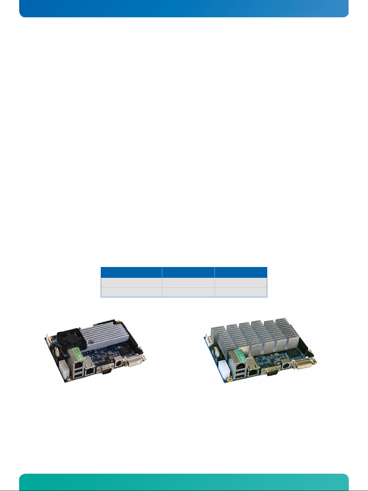
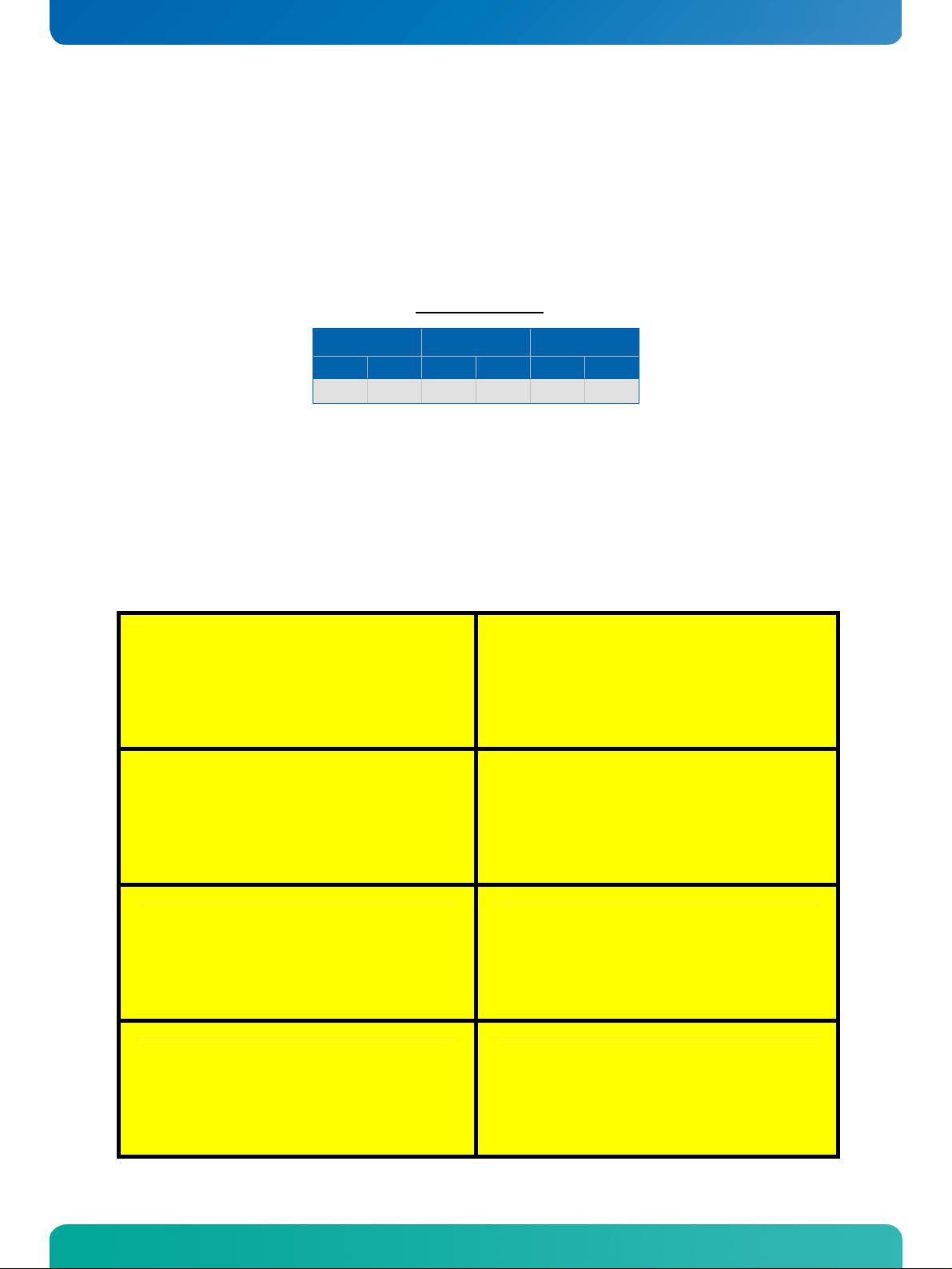
2.2 JRexplus-DC Overview
Please refer to the following matrix to choose the product that suits your needs best.
Article Number Active Cooling Passive Cooling
02008-0000-16-0
02008-0000-16-3
02008-0000-16-0 02008-0000-16-3
JRexplus-DC User's Guide
Page 9

KTD-S0008-F Page 4 Specifications
3 Specifications
3.1 Functional Specifications
Processor: Intel® ATOM™ N270
512 kB L2 cache
1.6 GHz clock frequency
Northbridge: Intel® 945GSE
533 MHz Front Side Bus (FSB)
One DDR2-533 unbuffered DDR-SDRAM (SODIMM form factor) up to 2 GB
Integrated Intel® GMA950 graphic controller with dual independent display support
Southbridge: Intel® ICH7M
Two channel Serial-ATA interface
Parallel-ATA PCI IDE controller
Eight USB channels (UHCI/EHCI) (seven channels available, one channel as PCI Express
MiniCard interface)
One LAN controller with LAN Connect Interface (LCI)
Two PCI Express ports (x1 lanes)
Integrated Intel® High Definition audio controller (HD audio)
External PCI bus with 32 bit / 33 MHz operation (PCI V2.3 compliant)
Onchip Video Graphics Array (VGA): Intel® GMA950
Intel® Gen 3.5 graphics engine
Dynamic Video Memory Technology (DVMT 3.0)
DirectX 9.0c support
Low Voltage Differential Signaling (LVDS) 18 bit dual channel interface up to UXGA display
resolution
Intel® Serial Digital Video Out (SDVO) with DVI monitor interface (maximal 160 MHz pixel
clock)
Analogue Video Graphics Array output (VGA/CRT) up to WUXGA resolution (DVI-I connector)
Onchip Parallel-ATA (P-ATA)
Supports PIO mode, Multiword DMA and Ultra DMA up to UDMA5
Compact Flash (CF) socket useable as master or slave
JRexplus-DC User's Guide
Page 10

KTD-S0008-F Page 5 Specifications
Onchip Serial-ATA (S-ATA)
Complies with Serial-ATA specification rev. 1.0a (Serial-ATA II)
Onchip Universal Serial Bus (USB)
Six ports are capable to handle USB 1.1 (UHCI) and USB 2.0 (EHCI)
Onchip High Definition Audio
Up to 24 bit sample resolution with 192 kHz sample rate
Onboard HD audio codec ALC888 (Realtek)
Supports LINE OUT, LINE IN, MICROPHONE IN and S/PDIF output
Onchip Fast Ethernet: Phy Intel® 82562ET
Fully compatible with IEEE 802.3
Gigabit Ethernet (PCI Express): Intel® 82574L
Full duplex operation at 10/100/1000 Mbps
Fully compliant with IEEE 802.3, IEEE 802.3u and IEEE 802.3ab
PCI Express MiniCard
One PCIe MiniCard slot on the bottom of the board allows the use of similar add-on devices
(PCI Express and USB interface)
PCI-104 Interface
33 MHz PCI clock and 32 bit data bus width
Only 3.3V PCI cards are supported
Super I/O (LPC): Winbond W83627EHG
One onchip thermal sensor and one remote temperature sensor (CPU)
One parallel port configurable as enhanced parallel port (EPP) and extended capabilities
One PS/2 keyboard and mouse controller
Two serial ports (RS232) COM1 and COM2
First serial port optionally as RS-422 or RS-485
Fan controller
Watchdog timer
JRexplus-DC User's Guide
Page 11

KTD-S0008-F Page 6 Specifications
Trusted Platform Module (LPC): Infineon SLB9635TT
Chipset LPC bus supports TPM 1.2 devices
Digital I/O (CPLD)
Eight bidirectional I/O lines, +3.3V signal level
BIOS: AMI®, 1 MB Flash BIOS
Real-Time Clock (RTC) with CMOS RAM and Battery
JRexplus-DC User's Guide
Page 12
KTD-S0008-F Page 7 Specifications
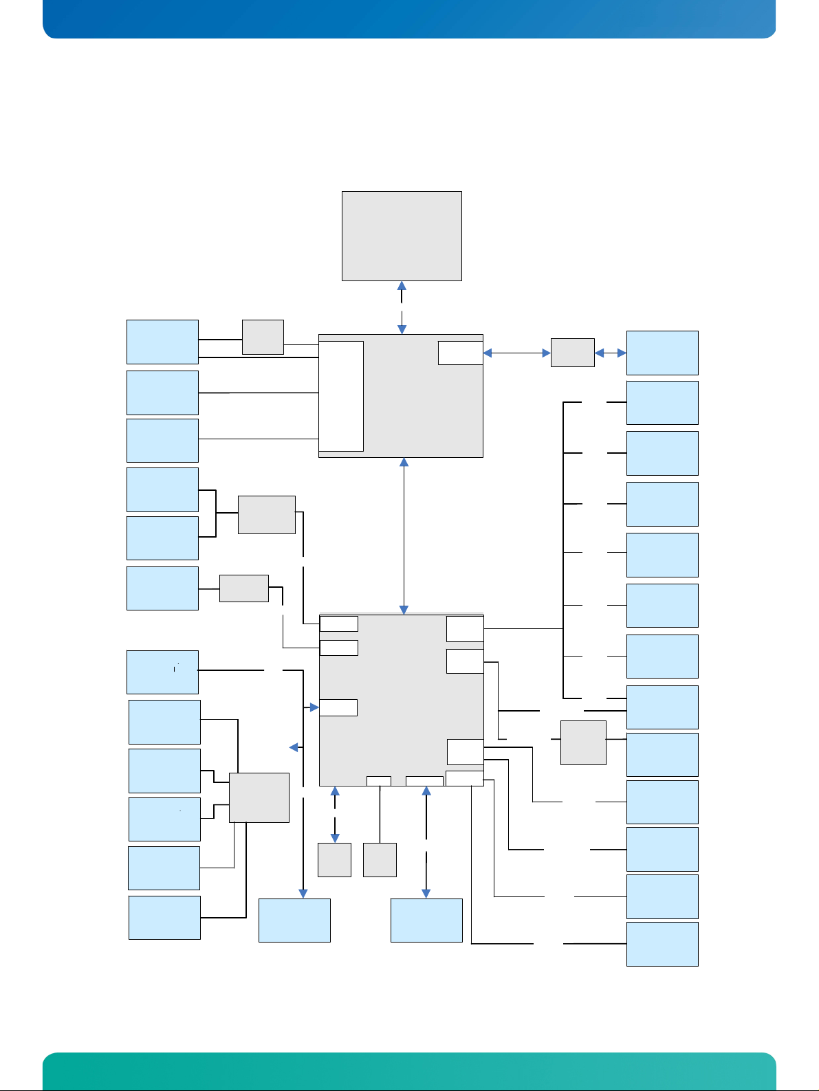
3.2 Block Diagram
JRexplus
J11
DVI-I
connector
J4
JILI30
connector
J96
backlight
connector
J23
Audio
Header
J98
SPDIF
connector
J20A
RJ45
connector
J33
Digital I/O
Header
J29
FAN
connector
J28
COM1
connector
J30
COM2
connector
J26
PS2
connector
(KB + MS)
J32
LPT
connector
SDVO to
HDA Codec
Ethernet
PHY
MAC/
Intel 82562ET
Super I
Controller
W83627DHG
-
DVI
CH7307C
ALC888
Eth 10/100
I/O
Winbond
DC
SDVO
VGA
LVDS
HDA
/
O
LPC
Trusted
Platform
Module
Graphic
Controller
HD Audio
Controller
Ethernet
Controller
LPC Bus
SPI
BIOS
Flash
CPU
N270
Diamondville
FSB 533
North Bridge
Intel 82945 GSE
South Bridge
Intel 82801 GBM
(ICH 7 M)
RTC
RTC
Battery
PCI Bus
PCI
J22
PC 104 Plus
connector
Memory
Controller
USB
Controller
PCI
Express
Ports
IDE
Controller
SATA
Controller
DDR 533
PCIe Port 0
DDR2
SDRAM
PCIe Port 1
Second IDE
SATA 0
SATA 1
USB 1
USB 2
USB 3
USB 4
USB 5
USB 6
USB 0
Gigabit
Ethernet
MAC / PHY
Intel 82574L
First IDE
7
J
SODIM-
Front USB
Front USB
USB Header
USB Header
USB Header
USB Header
MiniCard
connector
CF-Card
Pin Header
socket
J20B
J20B
J24
J24
J25
J25
J18
PCIe
J21
RJ45
J97
socket
J13
IDE
J15
SATA 0
J14
SATA 1
JRexplus-DC User's Guide
Page 13
KTD-S0008-F Page 8 Specifications
3.3 Mechanical Specifications
Dimensions
102 x 147 mm (4.0" x 5,8")
Height on top approx. 31 mm
Height on bottom approx. 6 mm
3.4 Electrical Specifications
Supply Voltage
The power supply connector (10 pins) requires +5V, +12V and +5V standby - alternative +5V only mode is
possible.
+5V DC ± 5%
+12V DC ± 5% (only necessary for LCD panel)
+5V DC standby ± 5%
Supply Voltage Ripple
Maximum 100mV peak to peak 0 – 20 MHz
Supply Current (DOS prompt)
Power consumption tests were executed during the DOS prompt with 1 GB DDR2 SDRAM, DVI monitor, USB
keyboard and CF card as boot device (default BIOS settings). The +12VDC line was not measured as this
voltage is only used to supply backlights through the backlight connector J96.
Article number 02008-0000-16-0
Supply voltage 5V
DOS Prompt
[A] [W] [A] [W]
1,74 8,7 0,15 0,76
Soft Off S5
JRexplus-DC User's Guide
Page 14
KTD-S0008-F Page 9 Specifications
Supply Current (Windows® XP SP3)
The power consumption tests were executed during Windows® 7 by using a tool to stress the CPU (100%
load) and extensive 3D graphic. The test was performed with 1 GB DDR2 SDRAM, DVI monitor, USB keyboard
& mouse and a S-ATA harddrive as boot device (default BIOS settings). The harddrive power consumption
was not measured within this test.
Article number 02008-0000-16-0
Supply voltage 5V
Full Load Idle Standby S3
[A] [W] [A] [W] [A] [W]
2,5 12,5 1,7 8,5 0,25 1,25
3.5 Real-Time Clock Battery
Voltage range: +2.4V - +3.6V (typ. +3.0V)
Maximum current 5μA @ +3.0V
Lithium battery precautions
CAUTION!
Danger of explosion if battery is incorrectly replaced. Replace only with same or equivalent t ype
recommended by manufacturer. Dispose of used
batteries according to the manufacturer’s instructions.
ATTENTION!
Risque d'explosion avec l'échange inadéquat de
la batterie. Remplacement seulement par le
même ou un type équivalent recommandé par le
producteur. L'évacuation des batteries usagées
conformément à des indications du fabricant.
ADVARSEL!
Lithiumbatteri – Eksplosionsfare ved fejlagtig
håndtering. Udskiftning må kun ske med batteri af
samme fabrikat og type. Levér det brugte batteri
tilbage til leverandøren.
VORSICHT!
Explosionsgefahr bei unsachgemäßem Aust ausch
der Batterie. Ersatz nur durch den selben oder
einen vom Hersteller empfohlenen gleichwertigen
Typ. Entsorgung gebrauchter Batterien nach Angaben des Herstellers.
PRECAUCION!
Peligro de explosión si la batería se sustituye
incorrectamente. Sustituya solamente por el
mismo o tipo equivalente recomendado por el
fabricante. Disponga las baterías usadas según
las instrucciones del fabricante.
ADVARSEL!
Eksplosjonsfare ved feilaktig skifte av batteri.
Benytt samme batteritype eller en tilsvarende type
anbefalt av apparatfabrikanten. Brukte batterier
kasseres i henhold til fabrikantens instruksjoner.
VARNING!
Explosionsfara vid felaktigt batteribyte. Använd
samma batterityp eller en ekvivalent typ som
rekommenderas av apparattillverkaren. Kassera
använt batteri enligt fabrikantens instruktion.
VAROITUS!
Paristo voi räjähtää, jos se on virheellisesti
asennettu. Vaihda paristo ainoastaan laltevalmistajan suosittelemaan tyyppiln. Hävitä käytetty
paristo valmistajan ohjeiden mukaisesti.
JRexplus-DC User's Guide
Page 15
KTD-S0008-F Page 10 Specifications
3.6 Environmental Specifications
Temperature
Operating:
Ambient temperature: 0 to +40°C (passive cooler with no airflow)
Ambient temperature: 0 to +60°C
Non operating:
Ambient temperature: -10 to +85°C
Note: 1) It is the customer's responsibility to provide sufficient airflow around each of the components to keep them within the
allowed temperature range.
1)
(active cooler with appropriate airflow)
Humidity
Operating: 10% to 90% (non condensing)
Non operating: 5% to 95% (non condensing)
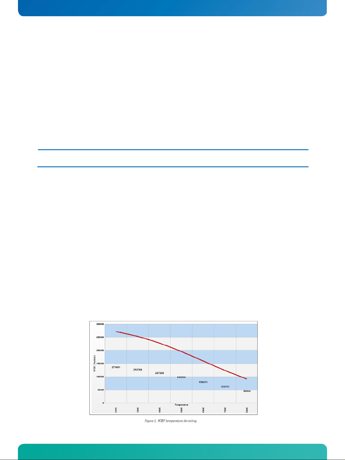
3.7 MTBF
The following MTBF (Mean Time Before Failure) values were calculated using a combination of
manufacturer’s test data, if the data was available, and the Telcordia (Bellcore) issue 2 calculation for the
remaining parts. The Telcordia calculation used is “Method 1 Case 3” in a ground benign, controlled
environment (GB,GC). This particular method takes into account varying temperature and stress data and
the system is assumed to have not been burned in. Figure 1 below shows MTBF de-rating for the E1
temperature range in an office or telecommunications environment. Other environmental stresses
(extreme altitude, vibration, salt water exposure etc.) lower MTBF values.
»System MTBF(hours) = 227228 @ 40°C
JRexplus-DC User's Guide
Page 16

KTD-S0008-F Page 11 Getting Started
Fans usually shipped with KONTRON Technology A/S products have 50,000-hour typical operating life. The
above estimates assume no fan, but a passive heat sinking arrangement. Estimated RTC battery life (as
opposed to battery failures) is not accounted for in the above figure and needs to be considered for
separately. Battery life depends on both temperature and operating conditions. When the Kontron unit has
external power; the only battery drain is from leakage paths.
All data is for information purposes only and not guaranteed for legal purposes. Subject to change without
notice. Information in this datasheet has been carefully checked and is believed to be accurate; however,
no responsibility is assumed for inaccuracies.
4 Getting Started
Getting started with the JRexplus-DC is very easy. Take the following steps:
Connect the ATX-adapter (KAB-ATX-10) or the delivered 5V adapter (KAB-ADAPT-ATXto5V) to
the JRexplus-DC 10pin ATX power connector J35. The location of connector J35 can be found
in the Appendix B.
Plug a suitable DDR2-SDRAM memory module into the RAM socket.
Connect a DVI monitor to the DVI connector (the use of a VGA monitor with a DVItoVGA
adapter is also possible).
Plug a keyboard and/or mouse to the PS/2 or USB connector(s).
Plug a Compact Flash card into the CF socket on the bottom of the board.
Connect an ATX power supply
Make sure all your connections have been made correctly. Turn on the power by shortening
the power button pins on the Front Panel Pin Header 1 (J36).
Enter the BIOS by pressing the Del key during boot-up. Make all changes in the BIOS Setup.
See the BIOS Setup chapter of this manual for details.
JRexplus-DC User's Guide
Page 17

KTD-S0008-F Page 12 System Memory
5 System Memory
The JRexplus-DC uses only 200 pin Small Outline Dual Inline Memory Modules (SODIMMs). One socket is
available for 1.8V unbuffered DDR2-533 SDRAM of up to 2 GB.
Memory modules with 667 MHz clock frequency can also be used. In this case the memory module is driven
with 533 MHz. It is recommended to use RAM modules which have been approved by KONTRON. Please
contact the board vendor to receive a list of approved memory modules.
The total amount of memory available on the SDRAM module is used for main memory and graphic memory
on the JRexplus-DC. S
graphic controller and processor. Therefore the full memory size is not available for software applications.
Up to 128 MB of system memory are used as graphic memory. Depending on system memory the graphic
driver may allocate more.
Attention: KONTRON Technology A/S can't guarantee the correct functionality of theJRexplus-DC when a DDR2-module with
another frequency than 533 Mhz is used.
hared Memory Architecture (SMA) manages the sharing of system memory between
6 PCI Bus Expansion
A quad-row socket trough-hole connector with a 2 x 2 mm (0.79" x 0.79") pitch implements the standard
32 bit PCI bus signals. The PCI-104 bus is available through the standard connector J22.
A description of signals, including electrical characteristics and timings, is beyond the scope of this document. Please refer to the official PCI bus and PC/104-plus specifications for more details.
Under no circumstances 5V PCI cards may be used on the JRexplus-DC board. Only Universal and 3.3V addon cards are permitted. V
JRexplus board due to a short curcuit with V
that this card is conform to these requirements.
Some PCI-104 extension cards might interfere mechanically with the CPU cooler. To avoid this and to
Note:
achieve the best possible cooling perfomance the usage of a PCI-104 spacer is recommended.
The usage of a PCI-104 to PCI adapter or riser card is not generally recommended. Due to consider-
Note:
able differences in between these third party adapter cards (e.g. different circuit path routing) the signal
integrity may suffer.
is set to 3.3V on the PCI bus. 5V PCI add-on cards can irretrievably damage the
I/O
. Before using a PCI add-on card please make absolutely sure
I/O
Attention: 5V PCI expansion cards can damage the board.
JRexplus-DC User's Guide
Page 18
KTD-S0008-F Page 13 Graphics Interface
7 Graphics Interface
The graphics interface supports DVI or CRT monitors and a variety of LCD panels with dual channels, color
depth of 18 bit and resolutions up to 1920x1200 for DVI/CRT and UXGA (1600x1200) for LCD.
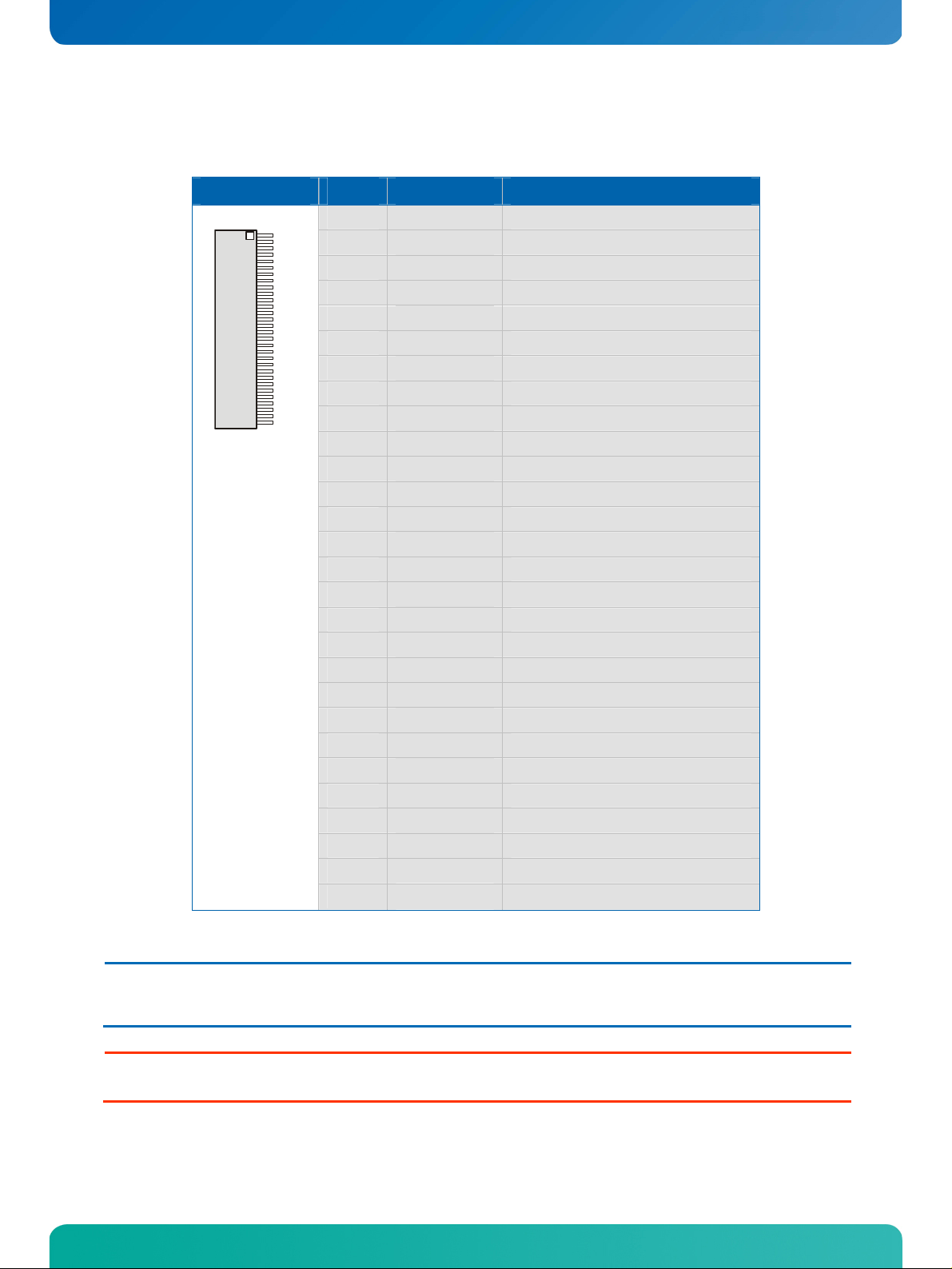
7.1 DVI or CRT Connector
The DVI and CRT interface are available through the standard 29 pin I style DVI connector J11.
Header Pin Signal Name Function
9
1
17
C3
C4
C1
C2
1 TMDS2- TMDS data 2 (negative)
2 TMDS2+ TMDS data 2 (positive)
3 GND Ground
4 N.C. Not connected
5 N.C. Not connected
6 DDC_CLK DDC clock
7 DDC_DATA DDC data
8 VSYNC Analog vertical sync
9 TMDS1- TMDS data 1 (negative)
10 TMDS1+ TMDS data 1 (positive)
11 GND Ground
12 N.C. Not connected
13 N.C. Not connected
14
15 GND Ground
16 TMDS_HPD Hot plug detect
17 TMDS0- TMDS data 0 (negative)
18 TMDS0+ TMDS data 0 (positive)
19 GND Ground
20 N.C. Not connected
21 N.C. Not connected
22 GND Ground
23 TMDS_CLK+ TMDS clock (positive)
24 TMDS_CLK- TMDS clock (negative)
C1 RED Analog red
C2 GRN Analog green
C3 BLU Analog blue
C4 HSYNC Analog horizontal sync
C5 GND Analog ground
VCC 1)
Power +5V
Note: 1) To protect the external power lines of peripheral devices make sure that
- the wires have the right diameter to withstand the maximum available current.
- to enclosure of the peripheral device fulfills the fire-protecting conditions of IEC/EN 60950.
JRexplus-DC User's Guide
Page 19
KTD-S0008-F Page 14 Graphics Interface
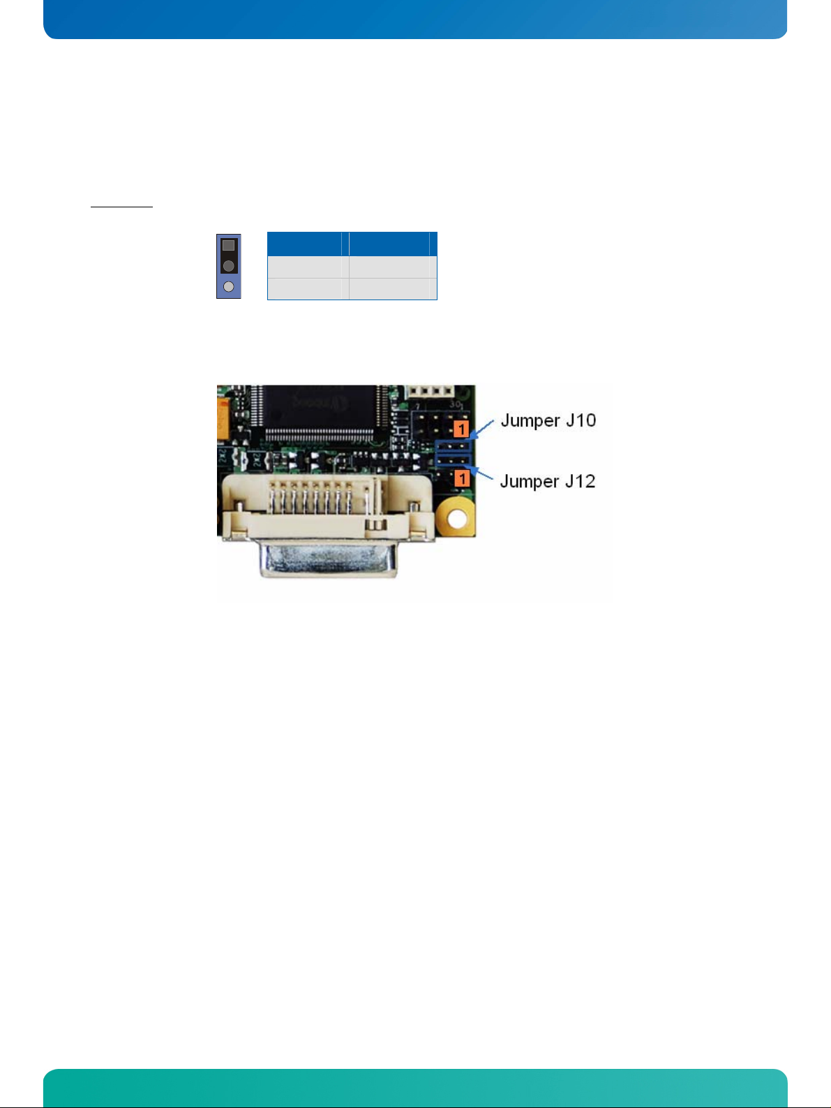
7.2 DDC Interpretation
Depending on the jumper settings of J10 and J12 the DDC data delivered by the display is either interpreted for the CRT channel or for the DVI channel.
Important
7.2.1 Jumper Setting
: Both jumpers (J10 and J12) must be set to the same position.
1
Pins DDC Signal
1 - 2 DVI
2 - 3 CRT
7.3 Flat Panel Connector
The LVDS interface for the flat panel is available through the JILI30 connector (30 pins) J4 on the bottom
side of the board. This connector represents the JILI interface. The implementation of this subsystem complies with the JILI specification of KONTRON Technology A/S. A variety of cables for different display types
are available from KONTRON.
JRexplus-DC User's Guide
Page 20
KTD-S0008-F Page 15 Graphics Interface
1
0
7.3.1 JILI30 Connector
Header Pin Signal Name Function
3
Note: 1) To protect the external power lines of peripheral devices make sure that
- the wires have the right diameter to withstand the maximum available current.
- to enclosure of the peripheral device fulfills the fire-protecting conditions of IEC/EN 60950.
1 FTX0- First channel data output 0 (negative)
2 FTX0+ First channel data output 0 (positive)
3 FTX1- First channel data output 1 (negative)
4 FTX1+ First channel data output 1 (positive)
5 FTX2- First channel data output 2 (negative)
6 FTX2+ First channel data output 2 (positive)
7 GND Ground
8 FTXC- First channel clock output (negative)
9 FTXC+ First channel clock output (positive)
10 FTX3- First channel data output 3 (negative)
11 FTX3+ First channel data output 3 (positive)
12 STX0- Second channel data output 0 (negative)
13 STX0+ Second channel data output 0 (positive)
14 GND Ground
15 STX1- Second channel data output 1 (negative)
16 STX1+ Second channel data output 1 (positive)
17 GND Ground
18 STX2- Second channel data output 2 (negative)
19 STX2+ Second channel data output 2 (positive)
20 STXC- Second channel clock output (negative)
21 STXC+ Second channel clock output (positive)
22 STX3- Second channel data output 3 (negative)
23 STX3+ Second channel data output 3 (positive)
24 GND Ground
25 SDA I2C data line
26 DATAENA Data enable output
27 SCL I2C clock line
28 - 30
VCC 1)
Power +3.3V or +5V
Warning: Check jumper J2 (panel power) for correct settings for your panel – not doing so might cause permanent damage
to your panel.
JRexplus-DC User's Guide
Page 21
KTD-S0008-F Page 16 Graphics Interface
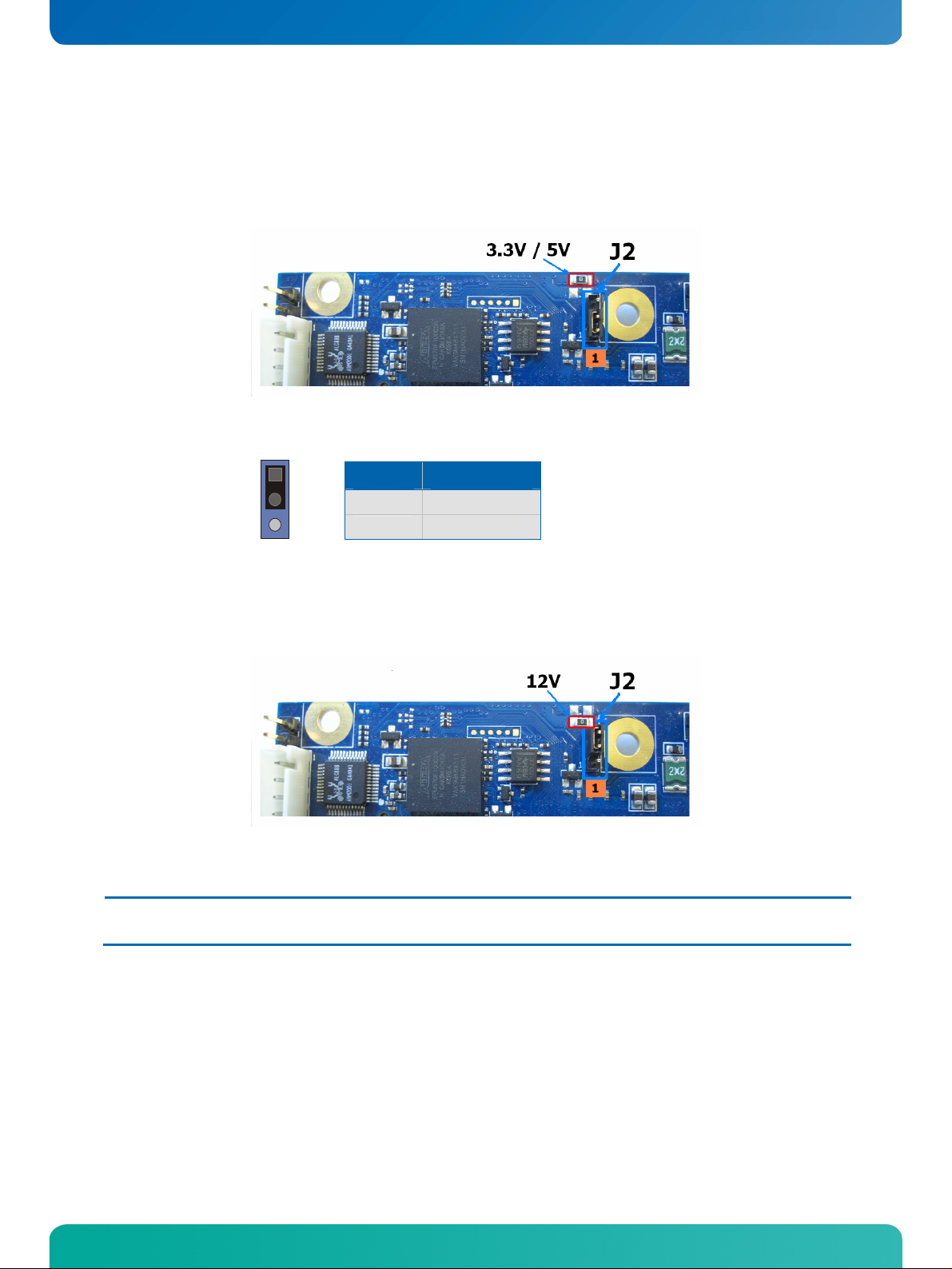
7.4 Panel Power
The panel power jumper J2 sets the panel supply voltage. For this setting a solder jumper is important. The
board is delivered with the solder jumper equipped as shown on the following picture.
In this case the board is configured so that 3.3V or 5V panel supply voltage can be selected with jumper J2.
1
Pins Supply Voltage
1 - 2
2 - 3
5V
3.3V
When a panel supply voltage of 12V is needed the solder jumper has to be set to the red marked position of
the following picture. It is important that only one of those two solder jumpers is equipped. When the 12V
solder jumper is set the 3.3V solder jumper has to be removed.
In this case the jumper setting (2-3) for 3.3V leads to a panel supply voltage of 12V.
Note: All soldering works must be done in a professional production environment. To avoid loosing the guarantee for your product
please contact the board vendor before you make any solder modification on the JRexplus-DC.
JRexplus-DC User's Guide
Page 22
KTD-S0008-F Page 17 Graphics Interface
7.5 Connecting a Flat Panel
To determine whether your flat panel is supported check the KONTRON website for panel lists. We regularly
update the list of panels that have been tested with the JRexplus-DC.
If you use one of those adapters supplied by KONTRON configuration is easy:
Check whether you have the correct adapter and cable for the panel you plan to use. Inspect
the cable for damages. Disconnect the power from your system.
Check jumper J2 for correct panel voltage.
Check jumper J5 for correct backlight voltage.
Check jumper J3 for correct backlight on/off polarity.
Connect the cable to the flat panel connector J4 on the JRexplus-DC and connect the other
end to your display.
Connect the backlight converter.
Supply power to your system.
If no image appears on your display connect a DVI monitor to the DVI connector.
If you still do not see improvement consider contacting the dealer for technical support.
7.6 Available Video Modes
The following list shows the video modes supported by the graphics controller with maximum frame buffer
size. When configured for saller frame buffers and/or using a flat panel on the JILI30 interface not all of
the video modes listed below may be available. Capability depends on system configuration and on display
capabilities. Different operating systems also may not support all listed modes by the available drivers.
Video Mode Type Characters/Pixels Colors
00h/01h Text 40 x 25 16
02h/03h Text 80 x 25 16
04h/05h Graphic 320 x 200 4
06h Graphic 640 x 200 2
07h Text 80 x 25 2
0Dh Graphic 320 x 200 16
0Eh Graphic 640 x 200 16
0Fh Graphic 640 x 350 2
10h Graphic 640 x 350 4
11h Graphic 640 x 480 2
12h Graphic 640 x 480 16
13h Graphic 320 x 200 256
JRexplus-DC User's Guide
Page 23
KTD-S0008-F Page 18 Graphics Interface
7.7 Extended VESA Modes
VESA Mode Type Pixels Colors
101h Graphic 640 x 480 256
103h Graphic 800 x 600 256
105h Graphic 1024 x 768 256
107h Graphic 1280 x 1024 256
111h Graphic 640 x 480 64k
112h Graphic 640 x 480 16M
114h Graphic 800 x 600 64k
115h Graphic 800 x 600 16M
117h Graphic 1024 x 768 64k
118h Graphic 1024 x 768 16M
11Ah Graphic 1280 x 1024 64k
11Bh Graphic 1280 x 1024 16M
7.8 Backlight Connector
Backlight is available through the J96 connector (7 pins). Backlight voltage and backlight on/off polarity
are controlled through the jumper J5 and J3. The backlight brightness (adjust voltage) can be set in the
BIOS Setup.
Header Pin Signal Name Function
Note: 1) To protect the external power lines of peripheral devices make sure that
- the wires have the right diameter to withstand the maximum available current.
- to enclosure of the peripheral device fulfills the fire-protecting conditions of IEC/EN 60950.
1 N.C. Not connected
2 BKLTADJ Brightness control (0V - 5V)
3 GND Ground
4
5
6 GND Ground
7 BKLTON Backlight on/off
VCC 1)
VCC 1)
Power +5V or +12V
Power +5V or +12V
JRexplus-DC User's Guide
Page 24
KTD-S0008-F Page 19 Graphics Interface
7.8.1 Jumper Settings
The jumper J5 can be used to set the backlight supply voltage to 5V or 12V.
1
Pins Backlight Voltage
1 - 2
2 - 3
5V
12V
The jumper J3 can be used to invert the backlight-on signal of the backlight inverter.
1
Pins Backlight-On
1 - 2
2 - 3
High
Low
JRexplus-DC User's Guide
Page 25

KTD-S0008-F Page 20 Serial Port Interfaces
6
6
8 Serial Port Interfaces
Two fully functional serial ports (COMA and COMB) provide asynchronous serial communications. COMA and
COMB support RS-232 operation modes. They are 16550 high-speed UART compatible and support 16-byte
FIFO buffers for transfer rates from 50 Baud to 115.2 kBaud. A programmable baud rate generator allows
transfer rates up to 1 MBaud.
One serial port is available as RS-232 on the JRex front panel and can be used as well as RS-422 or RS-485
interface, the second serial port COMB is available through a 10 pin header.
8.1 Connectors
COMA is available through the standard DSUB9 connector J28 (9 pins).
Header Pin Signal Name Function DSUB25
5
1
The same
connector J28 can be used as a RS-422 or RS-485 interface. The configuration is changeable in
the BIOS Setup.
5
1
9
Header Pin RS-422 RS-485 Function
9
1 /DCD Data carrier detect 8
2 RXD Receive data 3
3 TXD Transmit data 2
4 /DTR Data terminal ready 20
5 GND Ground 7
6 /DSR Data set ready 6
7 /RTS Request to send 4
8 /CTS Clear to send 5
9 /RI Ring indicator 22
1 TX- TX- / RX- Transmit data - / Receive data -
2 N.C. N.C. Not connected
3 TX+ TX+ / RX+ Transmit data + / Receive data +
4 N.C. N.C. Not connected
5 GND GND Ground
6 RX+ N.C. Receive data + / Not connected
7 N.C. N.C. Not connected
8 RX- N.C. Receive data - / Not connected
9 N.C. N.C. Not connected
Attention: A RS-422/RS-485 terminating resistor is not equipped on the JRexplus-DC.
JRexplus-DC User's Guide
Page 26

KTD-S0008-F Page 21 Serial Port Interfaces
COMB is available through the connector J30 (10 pins). A DSUB9 adapter cable is deliverable from KONTRON (KAB-DSUB9-3, part number 96061-0000-00-0).
Header Pin Signal Name Function DSUB9
1
Note: 1) To protect the external power lines of peripheral devices make sure that
- the wires have the right diameter to withstand the maximum available current.
- to enclosure of the peripheral device fulfills the fire-protecting conditions of IEC/EN 60950.
1 /DCD Data carrier detect 1
2 /DSR Data set ready 6
3 RXD Receive data 2
4 /RTS Request to send 7
5 TXD Transmit data 3
6 /CTS Clear to send 8
7 /DTR Data terminal ready 4
8 /RI Ring indicator 9
9 GND Ground 5
10
VCC 1)
Power +5V ---
JRexplus-DC User's Guide
Page 27
KTD-S0008-F Page 22 PS/2 Keyboard and Mouse Interface
9 PS/2 Keyboard and Mouse Interface
The Super-I/O of the JRexplus-DC supports a PS/2 keyboard and mouse. A PS/2 keyboard can be directly
connected to this interface. If you intend to use a PS/2 mouse connect a Y-cable to this interface. There are
many different Y-cables available on the market. Some cables have reverse keyboard/mouse signals. If your
keyboard and mouse do not work connect the keyboard to the mouse side and vice versa.
9.1 Connector
The keyboard/mouse interface is available through the standard miniDIN connector J26 (6 pins). A Y-cable
is deliverable from KONTRON (KAB-PS/2Y-1, part number 96001-0000-00-4)
Header Pin Signal Name Function
5
6
3
4
21
Note: 1) To protect the external power lines of peripheral devices make sure that
- the wires have the right diameter to withstand the maximum available current.
- to enclosure of the peripheral device fulfills the fire-protecting conditions of IEC/EN 60950.
1 KBDAT Keyboard data
2 MSDAT Mouse data
3 GND Ground
4
5 KBCLK Keyboard clock
6 MSCLK Mouse clock
VCC 1)
Power +5V (fused)
JRexplus-DC User's Guide
Page 28

KTD-S0008-F Page 23 USB Interface
10 USB Interface
The USB interface comes with six USB ports which follow the UHCI/EHCI specification and are USB 2.0
compliant. You can expand the amount of USB connections by adding external hubs. Two ports are available on a standard connector and four more ports on two pin strips.
10.1 Standard Connector
Two USB ports are available through the standard USB connector J20 (8 pins).
Header Pin Signal Name Function
1
5
1
2 USB1- USB port 1 (negative)
3 USB1+ USB port 1 (positive)
4 GND Ground
5
6 USB2- USB port 2 (negative)
7 USB2+ USB port 2 (positive)
8 GND Ground
VCC 1)
VCC 1)
Power +5V
Power +5V
10.2 Extension Connectors
The other USB ports are available through the standard pin strip connectors J24 and J25 (10 pins).
Header Pin Signal Name Function
Note: 1) To protect the external power lines of peripheral devices make sure that
- the wires have the right diameter to withstand the maximum available current.
- to enclosure of the peripheral device fulfills the fire-protecting conditions of IEC/EN 60950.
1
2
3 USB3/5- USB port 3 or 5 (negative)
4 USB4/6- USB port 4 or 6 (negative)
5 USB3/5+ USB port 3 or 5 (positive)
6 USB4/6+ USB port 4 or 6 (positive)
7 GND Ground
8 GND Ground
9 KEY (N.C.) Key pin
10 GND Ground
VCC 1)
VCC 1)
Power +5V
Power +5V
JRexplus-DC User's Guide
Page 29

KTD-S0008-F Page 24 USB Interface
An USB interface cable is available from KONTRON (KAB-DUSB, part number 821401).
10.3 USB Limitations
The power contacts for USB devices are protected. They are suitable to supply connected USB devices with a
maximum current of 500 mA. Do not supply external USB devices with higher power consumption through
these pins.
JRexplus-DC User's Guide
Page 30

KTD-S0008-F Page 25 EIDE Interface (P-ATA)
11 EIDE Interface (P-ATA)
The JRexplus-DC features one EIDE interface (up to UDMA5 mode) that can drive two hard disks. When two
devices share a single adapter they are connected in a master/slave, daisy-chain configuration. If only one
drive is connected you must set it as master. Alternatively the same interface can be used for Compact Flash
card applications.
The connector of the JRexplus-DC was intended for the use with a cable link. When a KONTRON chip-
Note:
disk or a CF card adapter is used the PCB's of these components point away from the board.
11.1 Connector
The EIDE interface is available through connector J13 (44 pins). It is designed in 2 mm grid for connectivity
to a 2.5” hard disk. You can use two cables to directly connect a disk in a 2.5” form factor (KAB-IDE-2MM,
part number 96021-0000-00-0) or a 3.5” form factor (KAB-IDE-25, part number 96020-0000-00-0).
Header Pin Signal Name Function Pin Signal Name Function
Note: 1) To protect the external power lines of peripheral devices make sure that
- the wires have the right diameter to withstand the maximum available current.
- to enclosure of the peripheral device fulfills the fire-protecting conditions of IEC/EN 60950.
2) Pin 28 is connected with 470
1 /RESET Reset 2 GND Ground
3 D7 Data 7 4 D8 Data 8
5 D6 Data 6 6 D9 Data 9
7 D5 Data 5 8 D10 Data 10
9 D4 Data 4 10 D11 Data 11
11 D3 Data 3 12 D12 Data 12
13 D2 Data 2 14 D13 Data 13
15 D1 Data 1 16 D14 Data 14
17 D0 Data 0 18 D15 Data 15
19 GND Ground 20 Key (N.C.) Key pin
21 DRQ DMA request 22 GND Ground
23 /IOW I/O write 24 GND Ground
25 /IOR I/O read 26 GND Ground
27 IOCHRDY I/O channel ready 28
29 /DACK DMA acknowledge 30 GND Ground
31 IRQ Interrupt request 32 N.C. Not connected
33 SA1 Address 1 34 ATAD UDMA detection
35 SA0 Address 0 36 SA2 Address 2
37 /CS1 Chip select 1 38 /CS3 Chip select 3
39 ACT Drive activity 40 GND Ground
41
43 GND Ground 44 N.C. Not connected
VCC 1)
Ω
to Ground for Cable Select IDE devices.
Power +5V 42
CSEL 2)
VCC 1)
Cable select
Power +5V
JRexplus-DC User's Guide
Page 31

KTD-S0008-F Page 26 EIDE Interface (P-ATA)
11.2 Compact Flash Card Interface
The same primary IDE channel is realized as a CF card interface, also capable of UDMA. The interface has
jumper options to be either a master or slave device. If for example the Compact Flash card is set to master
only a slave device can be connected to the 44 pin IDE connector.
11.2.1 Connector
The CF card interface is available through the standard CF connector J97 (50 pins).
Pin Signal Name Function Pin Signal Name Function
1 GND Ground 2 D3 Data 3
3 D4 Data 4 4 D5 Data 5
5 D6 Data 6 6 D7 Data 7
7 /CS1 Chip select 1 8 GND Ground
9 GND Ground 10 GND Ground
11 GND Ground 12 GND Ground
13
15 GND Ground 16 GND Ground
17 GND Ground 18 SA2 Address 2
19 SA1 Address 1 20 SA0 Address 0
21 D0 Data 0 22 D1 Data 1
23 D2 Data 2 24 N.C. Not connected
25 GND Ground 26 GND Ground
27 D11 Data 11 28 D12 Data 12
29 D13 Data 13 30 D14 Data 14
31 D15 Data 15 32 /CS3 Chip select 3
33 GND Ground 34 /IOR I/O read
35 /IOW I/O write 36
37 IRQ Interrupt 38
39 GND Ground 40 N.C. Not connected
41 /RESET Reset 42 IOCHRDY I/O channel ready
43 /DRQ DMA request 44 /DACK DMA acknowledge
45 ACT Drive activity 46 ATAD UDMA detection
47 D8 Data 8 48 D9 Data 9
49 D10 Data 10 50 GND Ground
VCC3 1)
Power +3.3V 14 GND Ground
VCC3 1)
VCC3 1)
Power +3.3V
Power +3.3V
JRexplus-DC User's Guide
Page 32

KTD-S0008-F Page 27 EIDE Interface (P-ATA)
11.2.2 Jumper Setting
Jumper J16 allows the configuration for master/slave mode.
1
Pins Signal
1 - 2
2 - 3
Master
Slave
Note: 1) To protect the external power lines of peripheral devices make sure that
- the wires have the right diameter to withstand the maximum available current.
- to enclosure of the peripheral device fulfills the fire-protecting conditions of IEC/EN 60950.
Warning: Inserting or removing the Compact Flash card while in operation can cause serious damage and must be avoided.
JRexplus-DC User's Guide
Page 33

KTD-S0008-F Page 28 Serial-ATA Interface (S-ATA)
12 Serial-ATA Interface (S-ATA)
The JRexplus-DC has two S-ATA ports. Serial-ATA connections boost the data rate theoretically up to 300
MB/sec. In addition it changes the parallel interface requiring 40 separate wires to a serial interface requiring only 6 wires. A RAID (R
12.1 Connector
The S-ATA interface is available through the standard L-type connectors J14 and J15 (7 pins).
Header Pin Signal Name Function
1
edundant Array of Independent Disks) configuration is not possible.
1 GND Ground
2 TX+ Transmit (positive)
3 TX- Transmit (negative)
4 GND Ground
5 RX- Receive (negative)
6 RX+ Receive (positive)
7 GND Ground
JRexplus-DC User's Guide
Page 34

KTD-S0008-F Page 29 LAN Controllers
13 LAN Controllers
The JRexplus-DC supports a Fast LAN PCI and a Gigabit PCI Express LAN controller.
13.1 Gigabit LAN Controller
The Gigabit LAN interface uses an Intel® 82574L PCI Express LAN controller. The controller support 10/
100/1000 Base-T interfaces. The devices auto-negotiates the use of a 10, 100 or 1000 Mbps connection.
Additionally it is possible to enable the LAN PXE Boot in the BIOS Setup to allow the system to boot up via a
network connection from a PXE server.
13.1.1 Connector
The LAN interface is available through the standard RJ45 connector J21 (8 pins).
Header Pin Signal Name Function
1
1 TXD+ / BI_D1+ 10/100 transmit / 1000 pair 1 (positive)
2 TXD- / BI_D1- 10/100 transmit / 1000 pair 1 (negative)
3 RXD+ / BI_D2+ 10/100 receive / 1000 pair 2 (positive)
4 BI_D3+ 1000 pair 3 (positive)
5 BI_D3- 1000 pair 3 (negative)
6 RXD- / BI_D2- 10/100 receive / 1000 pair 2 (negative)
7 BI_D4+ 1000 pair 4 (positive)
8 BI_D4- 1000 pair 4 (negative)
JRexplus-DC User's Guide
Page 35

KTD-S0008-F Page 30 LAN Controllers
13.2 Fast LAN Controller
The Fast LAN interface uses the ICH7 integrated PCI LAN controller in combination with the Intel® 82562V
LAN connect device. The controller support 10 and 100 Base-T interfaces. The devices auto-negotiates the
use of a 10 and 100 Mbps connection.
Additionally it is possible to enable the LAN PXE Boot in the BIOS Setup to allow the system to boot up via a
network connection from a PXE server.
13.2.1 Connector
The LAN interface is available through the RJ45 connector J20 (8 pins) that is combined with USB port 1/2.
Header Pin Signal Name Function
1
1 TXD+ 10/100 transmit (positive)
2 TXD- 10/100 transmit (negative)
3 RXD+ 10/100 receive (positive)
4 GND Ground
5 GND Ground
6 RXD- 10/100 receive (negative)
7 GND Ground
8 GND Ground
JRexplus-DC User's Guide
Page 36

KTD-S0008-F Page 31 PCI Express MiniCard
1
14 PCI Express MiniCard
PCI Express MiniCard (also known as Mini PCI Express, Mini PCIe and Mini PCI-E) is a replacement for the
Mini PCI form factor based on PCI Express. It is developed by the PCI-SIG. The host device supports both PCI
Express and USB 2.0 connectivity.
14.1 Connector
The interface is available through the standard PCI Express MiniCard connector J18 (52 pins).
Header Pin Signal Name Function Pin Signal Name Function
Note: 1) To protect the external power lines of peripheral devices make sure that
- the wires have the right diameter to withstand the maximum available current.
- to enclosure of the peripheral device fulfills the fire-protecting conditions of IEC/EN 60950.
1 /WAKE Wake event 2
3 N.C. Not connected 4 GND Ground
5 N.C. Not connected 6
7 /CLKREQ PCIe clock request 8 N.C. Not connected
9 GND Ground 10 N.C. Not connected
11 REFCLK- PCIe clock (neg.) 12 N.C. Not connected
13 REFCLK+ PCIe clock (pos.) 14 N.C. Not connected
15 GND Ground 16 N.C. Not connected
17 N.C. Not connected 18 GND Ground
19 N.C. Not connected 20 /W_DISABLE Wireless disable
21 GND Ground 22 /PERST PCIe reset
23 PERn0 PCIe receive (neg.) 24
25 PERp0 PCIe receive (pos.) 26 GND Ground
27 GND Ground 28
29 GND Ground 30 SMB_CLK SMBus clock
31 PETn0 PCIe transmit (neg.) 32 SMB_DATA SMBus data
33 PETp0 PCIe transmit (pos.) 34 GND Ground
35 GND Ground 36 USB- USB port 0 (neg.)
37 GND Ground 38 USB+ USB port 0 (pos.)
39
41
43 GND Ground 44 /LED_WLAN LED output
45 N.C. Not connected 46 /LED_WPAN LED output
47 N.C. Not connected 48
49 N.C. Not connected 50 GND Ground
51 N.C. Not connected 52
VCC3 1)
VCC3 1)
Power +3.3V 40 GND Ground
Power +3.3V 42 /LED_WWAN LED output
VCC3 1)
VCC1 1)
VCC3AUX 1)
VCC1 1)
VCC1 1)
VCC3 1)
Power +3.3V aux
Power +3.3V
Power +1.5V
Power +1.5V
Power +1.5V
Power +3.3V
JRexplus-DC User's Guide
Page 37

KTD-S0008-F Page 32 Audio Interface
15 Audio Interface
The JRexplus-DC supports a HD audio codec with 24 bit resolution and 192 kHz sample rate. The interface
includes LINE OUT, LINE IN, MICROPHONE IN and a digital S/PDIF output. The HD audio controller is a bus
mastering PCI device which is physically connected to one or more codecs via the HD Audio link. It contains
®
one or more DMA engines. For signal levels see the High Definition audio specification (Intel
15.1 Hardware Features
Parameter Values Units
Output resolution (LINE OUT, S/PDIF) 16/20/24 bit
Output sample rate (LINE OUT, S/PDIF) 44.1/48/96/192 kHz
Output Signal-to-Noise Ratio (LINE OUT) 97 dB
Output current (S/PDIF)
Input resolution (LINE IN) 16/20 bit
Input sample rate (LINE IN) 44.1/48/96 kHz
Input Signal-to-Noise Ratio (LINE IN) 90 dB
12 @ 75Ω
).
mA
15.2 Connector
The analog audio interface is available through the connector J23 (6 pins). A prototype adapter cable
(open ended) is deliverable from KONTRON (KAB-SOUND-CMP-2, part number 96063-0000-00-1).
Header Pin Signal Name Function
1 LINE_OUT_R Line output right
2 GND Ground
3 LINE_OUT_L Line output left
4 LINE_IN_R Line input right
5 MIC_IN Microphone input
6 LINE_IN_L Line input left
15.3 Digital Connector (S/PDIF)
The digital audio output is available through the pin strip J98 (2 pins).
Header Pin Signal Name Function
1
1 SPDIF_OUT S/PDIF output
2 GND Ground
JRexplus-DC User's Guide
Page 38

KTD-S0008-F Page 33 Digital I/O Interface
0
16 Digital I/O Interface
The JRexplus-DC features eight bidirectional I/O lines. All I/O lines are TTL tolerant. Inputs can be driven
from either +3.3V or +5V devices. This feature allows a mixed +3.3V / +5V system environment.
16.1 Electrical Specifications
Digital Inputs
Parameter Min. Typ. Max. Units
Input LOW voltage +0.8 V
Input HIGH voltage +1.7 +5.5 V
Input rate (direct access) 100 kHz
Digital Outputs
Parameter Min. Typ. Max. Units
Output LOW voltage +0.45 V
Output HIGH voltage +2.4 +3.3 V
Output LOW/HIGH current 16 mA
Switching rate (direct access) 100 kHz
16.2 Connector
The digital I/O interface is available through the connector J33 (10 pins).
Header Pin Signal Name Function
1 2
91
1
2 GPIO0 Bidirectional I/O 0
3 GPIO1 Bidirectional I/O 1
4 GPIO2 Bidirectional I/O 2
5 GPIO3 Bidirectional I/O 3
6 GPIO4 Bidirectional I/O 4
7 GPIO5
8
9
10 GND Ground
VCC 1)
GPIO6
GPIO7
Power +3.3V
Bidirectional I/O 5
Bidirectional I/O 6
Bidirectional I/O 7
Note: 1) To protect the external power lines of peripheral devices make sure that
- the wires have the right diameter to withstand the maximum available current.
- to enclosure of the peripheral device fulfills the fire-protecting conditions of IEC/EN 60950.
2) The voltage level is not specified by the manufacturer
JRexplus-DC User's Guide
Page 39

KTD-S0008-F Page 34 Parallel Port Interface
2
17 Parallel Port Interface
The JRexplus-DC incorporates a parallel port that can be set to uni-/bidirectional and supports EPP/ECP
operating modes.
17.1 Connector
The parallel port is available through the connector X20 (32 pins). A DSUB25 adapter cable is deliverable
from KONTRON (KAB-DSUB25-2, part number 61033).
Header Pin Signal Name Function DSUB25
1
3
Note: 1) To protect the external power lines of peripheral devices make sure that
- the wires have the right diameter to withstand the maximum available current.
- to enclosure of the peripheral device fulfills the fire-protecting conditions of IEC/EN 60950.
1
12 /AFD Autofeed 14
13 /STB Strobe 1
14 /ERR Error 15
15 D0 Data 0 2
16 /INIT Init 16
18 D1 Data 1 3
19 /SLIN Select in 17
20 D2 Data 2 4
21 D3 Data 3 5
23 D4 Data 4 6
24 D5 Data 5 7
25 D6 Data 6 8
26 D7 Data 7 9
28 /ACK Acknowledge 10
29 /BUSY Busy 11
30 PE Paper out 12
31 /SLCT Select out 13
2, 11 GND Ground 18 - 25
17, 22 GND Ground 18 - 25
27,32 GND Ground 18 - 25
VCC 1)
Power +5V N.C.
JRexplus-DC User's Guide
Page 40
KTD-S0008-F Page 35 Power Supply
6
18 Power Supply
The JRexplus-DC supports the ATX power supply mode and 5V only mode.
18.1 Connector
The power connector is available as J35 (10 pins). For both the ATX and the 5V only mode an adapter cable
is deliverable from KONTRON. For the ATX mode this is KAB-ATX-10 (part number 96072-0000-00-0). For
the 5V only mode the adapter cable KAB-ADAPT-ATXto5V (P/N96072-0000-05-2) can be used. This cable is
delivered with every JRexplus-DC. This cable allows to supply the board with 5V and 12V DC.
Header Pin Signal Name Function
1
1 PS_ON Power supply on
2 GND Ground
3 GND Ground
4
5 NC Not connected
6
7
8
9
10 GND Ground
VCC12 1)
VCC5SB 1)
VCC5 1)
VCC5 1)
VCC12# 1)
+12V
+5V standby
+5V
+5V
-12V
Note: 1) To protect the external power lines of peripheral devices make sure that
- the wires have the right diameter to withstand the maximum available current.
- to enclosure of the peripheral device fulfills the fire-protecting conditions of IEC/EN 60950.
18.2 Power Pins
Every power pin on the power connector supplement is limited to a maximum current and the following
limitations apply.
Power Number of Pins Max. Current per Pin
VCC5 2 Tbd
VCC12 1 Tbd
VCC5SB 1 Tbd
JRexplus-DC User's Guide
Page 41

KTD-S0008-F Page 36 Power Supply
0
18.3 Power Front Panel Header
The power button and other power signals are available through the pin strip J36 (10 pins).
Header Pin Signal Name Function
1 2
91
1 PWR_LED+ Power LED (positive)
2 PWR_BTN+ Power button (positive)
3 N.C. Not connected
4 PWR_BTN- Power button (negative)
5 PWR_LED- Power LED (negative)
6 N.C. Not connected
7 KBD_LOCK Keyboard lock
8 RSVD Reserved
9 GND Ground
10 RSVD Reserved
17.3.1 Power LED
The following picture illustrates the onboard wiring.
Power LED
+5V
470R
+
Connector
JRexplus-DC User's Guide
Page 42

KTD-S0008-F Page 37 Common Front Panel Pins
19 Common Front Panel Pins
The Common Front Panel provides some special functions (e.g. reset button and speaker).
19.1 Pin Strip
The Common Front Panel is available through the pin strip J37 (8 pins).
Header Pin Signal Name Function
1
7
2
8
The reset signal of the JRexplus-DC is edge-controlled. This means the board can not be hold within the
reset.
1 RST_BTN+ Reset button (positive)
2 SPKR+ Speaker (positive)
3 RST_BTN- Reset button (negative)
4 N.C. Not connected
5 HDD_LED+ Harddisk LED (positive)
6 N.C. Not connected
7 HDD_LED- Harddisk LED (negative)
8 SPKR- Speaker (negative)
18.1.1 Harddisk LED
The following picture illustrates the onboard wiring.
Harddisk LED
+3.3V
1k0
+
Connector
JRexplus-DC User's Guide
Page 43

KTD-S0008-F Page 38 Crisis Management
20 Crisis Management
Modifying parameters in the BIOS Setup implies the risk of leaving your system in an unbootable state. In
case this happens one jumper exists to reset the settings to 'Fail-Safe' values.
To Reset to 'Fail-Safe' values please take the following steps:
Power down the board
Jumper J101 must be set
Power up the board - BIOS Setup enters automatically
Before saving your new settings with 'Save Changes and Exit' remove the jumper
The board should be functional again now
21 Autostart Function
When the JRexplus-DC should start directly when the power is applied (without a power button signal) the
autostart jumper J102 must be set.
JRexplus-DC User's Guide
Page 44

KTD-S0008-F Page 39 Power and Thermal Management
22 Power and Thermal Management
22.1 SpeedStep Technology
The Intel® Atom processor offers the Intel® Enhanced SpeedStepTM technology that automatically switches
between maximum performance mode and battery optimized mode depending on the needs of the application being run. When powered by a battery or running in idle mode the processor drops to lower frequencies conserving battery life while maintaining a high level of performance. The previous frequency is
set back automatically when the operating mode changes.
22.2 C-State Control
The Intel® chipset has been implemented the control for dynamically starting and stopping system clocks
and power. The states are passing through C0 (full on) to C4 one after another. The C-state ends when a
break event occurs (e.g. an IRQ or SMI).
22.3 Hyper-Threading Technology
Intels® Hyper-Threading technology boosts system performance without higher clock rates or adding more
processors which is also an optimization of the power consumption. Hyper-Threading works by duplicating
instructions streams, called threads. This allows a CPU to pretend to be two logical processors on the
operating system which must support this technology. Individually the logical processors can be halted or
interrupted or can execute a thread independently of the other logical unit.
22.4 Fan Interface
If a fan is added use this interface to connect a fan to cool off the CPU. The connector only supports 5V
fans. A three pin fan includes a pulse output (sense) which allows the control of fan speed.
22.4.1 Connector
The fan interface is available through connector J29.
Header Pin Signal Name Function
1 SENSE Speed monitoring
2
3 GND Ground
VCC 1)
Power +5V
Note: 1) To protect the external power lines of peripheral devices make sure that
- the wires have the right diameter to withstand the maximum available current.
- the enclosure of the peripheral device fulfills the fire-protecting conditions of IEC/EN 60950.
JRexplus-DC User's Guide
Page 45

KTD-S0008-F Page 40 Setup Guide
23 Setup Guide
The module is equipped with AMI® BIOS which is located in an onboard flash memory. You can update the
BIOS using a flash utility.
23.1 Determining the BIOS Version
Whenever you contact technical support about BIOS issues providing a BIOS version <BDCPR???> is espe-
®
cially helpful. To determine the AMI
looks at main menu (additional information are available with submenu Module Info):
Bios Info
BIOS Version : BDCPR???
Build Date : ??/??/??
BIOS version press the DEL key on your keyboard during boot-up and
23.2 Start AMI® BIOS Setup Utility
To start the AMI® BIOS Setup utility press <DEL> when the following string appears during boot-up.
Press <DEL> to run Setup
The main menu then appears.
The Setup screen is composed of several sections:
Setup Screen Location Function
Menu Bar
Legend Bar
Item Specific Help Window
Menu Window
General Help Window
Menu Bar
The menu bar at the top of the window lists different menus. Use the left/right arrow keys to make a selection.
Top Lists and selects all top level menus
Right side bottom Lists Setup navigation keys
Right side top Help for selected item
Left center Selection fields for current menu
Overlay (center) Help for selected menu
JRexplus-DC User's Guide
Page 46

KTD-S0008-F Page 41 Setup Guide
Legend Bar
Use the keys listed in the legend bar on the bottom to make your selections or exit the current menu. The
table below describes the legend keys and their alternates.
Key Function
<F1> or <Alt-H>
<Esc>
← or → Arrow key
↑ or ↓ Arrow key
<Home> or <End>
<PgUp> or <PgDn>
<F9>
<F10>
<Enter>
<Alt-R>
Selecting an Item
Use the ↑ or ↓ key to move the cursor to the field you want. Then use the + and – keys to select a value for
that field.
Displaying Submenus
Use the ← or → key to move the cursor to the submenu you want. Then press <Enter>. A pointer ()
marks all submenus.
Item Specific Help Window
The help window on the right side of each menu displays the help text for the selected item. It updates as
you move the cursor to each field.
General Help Window
Pressing <F1> or <Alt-F1> on a menu brings up the general help window that describes the legend keys and
their alternates. Press <Esc> to exit the general help window.
General help window
Exit menu
Select a menu
Select fields in current menu
Move cursor to top or bottom of current window
Move cursor to next or previous page
Load the default configuration values for this menu
Save and exit
Execute command or select submenu
Refresh screen
JRexplus-DC User's Guide
Page 47

KTD-S0008-F Page 42 Setup Guide
23.3 Menu Bar
Feature Description
Main Define time and date and show service information
Advanced Configuration of all onboard devices (e.g. CPU, IDE, LAN, USB, Display)
PCIPnP Define PCI/Legacy IRQs and other PnP settings
Boot Define the boot sequence and special boot settings
Security Change, set or disable supervisor/user passwords
Exit Exit Setup with/without saving or set default values
23.4 Main Menu
Feature Option Description
BIOS Version N / A Show the actual BIOS release
AMI Core8 Version N / A Show the AMI® core version
Build Date N / A Show the BIOS build date
Module Info Submenu Show additional service information
8
System Time HH:MM:SS Set the system time
System Date MM/DD/YYYY Set the system date
22.4.1 Module Info Submenu
Feature Option Description
Board Name N / A Show the KONTRON specific board name
Board Class N / A Show the KONTRON specific board class
Serial Number N / A Show the KONTRON specific serial number
Manufacturing Date N / A Show the KONTRON specific manufacturing date
Hardware Version N / A Show the KONTRON specific hardware version
Boot Counter N / A Display the boot counter
Processor Name N / A Show the processor identifier
Processor Speed N / A Show the actual CPU boot speed
Processor Count N / A Show the number of CPU's
CPU Stepping N / A Show the CPU silicon stepping
CPU Microcode Rev. N / A Show the CPU microcode revision
System Memory Size
NB Stepping
SB Stepping
N / A Display amount of conventional memory detected during
boot-up
N / A Show the North Bridge (945GSE) silicon stepping
N / A Show the South Bridge (ICH7M) silicon stepping
JRexplus-DC User's Guide
Page 48

KTD-S0008-F Page 43 Setup Guide
23.5 Advanced Menu
Feature Option Description
CPU Configuration Submenu
8
Onboard Device
8
Configuration
Display Control Submenu
8
ACPI Configuration Submenu
8
Miscellaneous
8
Configuration
Submenu Configure most onboard devices (e.g. IDE, LAN, USB)
Submenu Configure additional important settings
22.5.1 CPU Configuration Submenu
Feature Option Description
Manufacturer
Processor Name
Frequency
FSB Speed
Cache L1
Cache L2
Ratio Actual Value
Max CPUID Value Limit Disabled
Execute-Disable Bit
Capability
Hyper-Threading
Technology
DTS-based Thermal
Management
DTS Calibration
Intel(R) SpeedStep(tm)
tech
Intel(R) C-STATE tech
Enhanced C-States
N / A
N / A
N / A
N / A
N / A
N / A
N / A
Enabled
Disabled
Enabled
Disabled
Enabled
Disabled
Enabled
Disabled
Enabled
Disabled
Enabled
Disabled
Enabled
Disabled
Enabled
Configure special CPU features
Set the display features (including panel parameters)
Set some ACPI defaults
Show the processor manufacturer
Show the processor identifier
Show the actual CPU boot speed
Show the speed of the Front Side Bus
Show the L1 cache size
Show the L1 cache size
Show the actual CPU ratio
Limit CPUID functions
This option can help to prevent certain classes of buffer
overflow errors (AMD® NX-bit or Intel® XD-bit)
Enable or disable the two logical processor mode
Enable or disable the thermal management utilizing the CPU
Digital Thermal Sensor
During POST the BIOS calibrate the Digital Thermal Sensor
Let customize performance computing. The processor can
drop to a lower frequency and voltage
Enable or disable power saving modes (a C-STATE is an idle
state). C0 is the operational state, C1 to C4 represents the
saving modes
Enable or disable the enhanced power saving modes (C1E to
C4E)
JRexplus-DC User's Guide
Page 49
KTD-S0008-F Page 44 Setup Guide
22.5.2 Onboard Device Configuration Submenu
Feature Option Description
North Bridge
8
Configuration
South Bridge
8
Configuration
PCI Express
8
Configuration
IDE Configuration
8
Ethernet Configuration
8
USB Configuration
8
SuperIO Configuration
8
Trusted Computing
8
Submenu Configure the North Bridge (945GSE) features
Submenu Configure the South Bridge (ICH7M) features
Submenu Configure the PCI Express support
Submenu Configure the IDE devices (P-ATA, S-ATA)
Submenu Configure the LAN controllers
Submenu Configure the USB support
Submenu Configure the Super-I/O (PS/2, serial and parallel port)
Submenu Configure the Trusted Computing (TPM)
22.5.2.1 North Bridge Submenu
Feature Option Description
DRAM Frequency Auto, 400 MHz
Configure DRAM Timing
by SPD
DRAM CAS# Latency 5, 4, 3
DRAM RAS# to CAS# Delay
DRAM RAS# Precharge
DRAM RAS# Activate to
Precharge
Memory Hole Disabled
Chipset Thermal
Throttling
DT in SPD Disabled
TS on DIMM Disabled
533 MHz
Disabled
Enabled
2 DRAM Clocks
3 DRAM Clocks
4 DRAM Clocks
5 DRAM Clocks
6 DRAM Clocks
7 DRAM Clocks
4 DRAM Clocks
to
15 DRAM Clocks
15MB-16MB
Disabled
Enabled
Enabled
Enabled
Define the maximum memory speed (DDR2-400 or DDR2-
533)
Disabled allows the manual configuration of DRAM timing
Configure the DRAM CAS latency
Configure the DRAM RAS to CAS delay and the DRAM RAS precharge value
Configure the DRAM RAS activate to precharge value
Enable or disable the memory hole at 15 MB
Enable or disable the thermal throttling. Initialize thermal
management with default trip point temperatures
Support the Delta Temperature in the DRAM SPD thermal
management algorithm
Support the Thermal Sensor on DIMM thermal management
functionality
JRexplus-DC User's Guide
Page 50

KTD-S0008-F Page 45 Setup Guide
22.5.2.2 South Bridge Submenu
Feature Option Description
Audio Controller Auto
Azalia
AC'97 Audio and
Modem
All Disabled
SMBUS Controller Enabled
Disabled
Reserved Page Route
SLP_S4# Min. Assertion
Width
Restore on AC Power Loss Power Off
PCI
LPC
4 to 5 Seconds
3 to 4 Seconds
2 to 3 Seconds
1 to 2 Seconds
Power On
Last State
Allow the fixed selection of 24 bit HD audio (Azalia) or 16 bit
AC'97 audio
Enable or disable the SMBus controller (interact with digital
I/O and DRAM SPD)
Determine the route of port 80h, 84h-86h, 88h and 8Ch-8Eh
to LPC or PCI
Power management feature
Power management feature. Select behavior after AC power
loss
22.5.2.3 PCI Express Submenu
Feature Option Description
Active State Power
Management
PCIE Port 0
PCIE Port 1
PCIE Port 0 IOxAPIC
Enable
PCIE Port 1 IOxAPIC
Enable
Disabled
Enabled
Auto
Enabled
Disabled
Disabled
Enabled
Enable or disable PCI Express L0s and L1 link power state
Enable or disable PCI Express ports and the associated devices
Enable or disable the I/O APIC feature
JRexplus-DC User's Guide
Page 51

KTD-S0008-F Page 46 Setup Guide
22.5.2.4 IDE Configuration Submenu
Feature Option Description
ATA/IDE Configuration
Legacy IDE Channels
Configure SATA as Disabled
Configure SATA as IDE
Configure SATA Channels Before PATA
Primary IDE Master
8
Primary IDE Slave
8
Secondary IDE Master
8
Secondary IDE Slave
8
Third IDE Master
8
Third IDE Slave
8
Hard Disk Write Protect Disabled
IDE Detect Time Out (Sec)
ATA(PI) 80Pin Cable
Detection
Disabled
Compatible
Enhanced
SATA Only
SATA Pri, PATA Sec
PATA Only
RAID
RAID
AHCI
Behind PATA
Submenu Display the status of autodetection
Submenu Display the status of autodetection
Submenu Display the status of autodetection
Submenu Display the status of autodetection
Submenu Display the status of autodetection
Submenu Display the status of autodetection
Enabled
0, 5, 10, 15
20, 25, 30, 35
Host&Device
Host
Device
The entry 'Enhanced' allow more detailed SATA settings
Only visible if 'ATA/IDE Configuration' is set to 'Compatible'. Enable or disable the PATA or SATA controller
Only visible if 'Legacy IDE Channels' is set to 'PATA Only'
Only visible if 'ATA/IDE Configuration' is set to 'Enhanced'.
Configure the SATA controller in native (IDE), RAID or AHCI
mode
Only visible if 'ATA/IDE Configuration' is set to 'Enhanced'
and 'Configure SATA as' is set to 'IDE'. Define the detection
order
Allow the write protection of harddisk devices. Only valid if
the device is accessed through the BIOS
Select the time out value for the detection of ATA(PI)
devices
Select the mechanism for detecting 80 pin cable
JRexplus-DC User's Guide
Page 52

KTD-S0008-F Page 47 Setup Guide
22.5.2.4.1 Primary/Secondary/Third Master/Slave Submenu
Feature Option Description
Device
Vendor
Size
LBA Mode
Block Mode
PIO Mode
Async DMA
Ultra DMA
S.M.A.R.T.
Type Not Installed, Auto
LBA/Large Mode
Block (Multi-Sector
Transfer)
PIO Mode Auto
DMA Mode Auto
S.M.A.R.T. Auto
32Bit Data Transfer Disabled
Not Detected
Hard Disk
ATAPI CDROM
ARMD
N / A Show the IDE drive manufacturer and drive name
N / A Display the calculated size of the drive
Supported
Not Supported
N / A Display the block size (in sectors) or 'Not Supported'
Not Supported,
0, 1, 2, 3, 4
Not Supported
SingleWord DMA0 - 2
MultiWord DMA0 - 2
Not Supported
Ultra DMA0 - 6
Supported
Not Supported
CD/DVD, ARMD
Disabled
Auto
Disabled
Auto
0, 1, 2, 3, 4
SWDMA0 - 2
MWDMA0 - 2,
UDMA0 - 6
Disabled
Enabled
Enabled
Show the type of IDE drive
ARMD = ATAPI Removable Media Device
Show whether a disk uses LBA
Display the highest supported PIO mode
Display the highest supported Async DMA mode
Display the highest supported Ultra DMA mode
Show whether a disk uses S.M.A.R.T. (Self Monitoring,
Analysis and Reporting Technology)
Define the type of the IDE drive
LBA causes Logical Block Addressing
Block mode enables multi-sector transfer and increase the
performance
Define the PIO mode if DMA not possible. Auto selects the
optimum transfer mode
Define the Async or Ultra DMA mode. Auto selects the
optimum transfer mode
Show if the device is capable of using the error predediction tool
Enable 32 bit communication between CPU and IDE
controller
JRexplus-DC User's Guide
Page 53

KTD-S0008-F Page 48 Setup Guide
22.5.2.5 Ethernet Configuration Submenu
Feature Option Description
Gigabit Ethernet Port Enabled
Fast Ethernet Port Enabled
Enable GbE Ethernet PXE
Rom
Enable Fast Ethernet PXE
Rom
22.5.2.6 USB Configuration Submenu
Feature Option Description
Module Version N / A
USB Devices Enabled N / A
USB Functions
2 USB Ports
4 USB Ports
6 USB Ports
8 USB Ports
USB 2.0 Controller Enabled
Legacy USB Support
Port 64/60 Emulation
USB 2.0 Controller Mode
BIOS EHCI Hand-Off
Hotplug USB FDD Support
USB Mass Storage
8
Device Configuration
Disabled
Disabled
Enabled
Disabled
Enabled
Disabled
Disabled
Disabled
Disabled
Enabled
Auto
Disabled
Enabled
FullSpeed
HiSpeed
Disabled
Enabled
Disabled
Enabled
Auto
Submenu Display the status of USB mass storage devices
Enable or disable the Gigabit Ethernet controller
Enable or disable the Fast Ethernet controller
Enable or disable the option ROM to allow LAN boot functionality for the Gigabit Ethernet controller
Enable or disable the option ROM to allow LAN boot functionality for the Fast Ethernet controller
Show USB module version
Show detected USB devices
Enable or disable the USB ports
Enable or disable the USB 2.0 controller (EHCI)
Enable support for legacy USB devices (e.g. keyboard and
mouse). 'Auto' disables legacy support if no devices are connected
Allow the complete USB keyboard legacy support
Set the USB 2.0 controller to HiSpeed (480 Mbps) or FullSpeed (12 Mbps) for legacy mode
This patch must be allied for operating systems before WIN
XP which have problems gaining control over USB 2.0 ports.
If enabled this provides a simple semaphore based mechanism for exchanging EHCI ownership
A dummy FDD device is created that will be associated with a
hot-plugged FDD later. 'Auto' creates this device only if
there is no USB FDD present
JRexplus-DC User's Guide
Page 54

KTD-S0008-F Page 49 Setup Guide
22.5.2.6.1 USB Mass Storage Device Configuration Submenu
Feature Option Description
USB Mass Storage Reset
Delay
Device N / A
Emulation Type Auto
10 Sec.
20 Sec.
30 Sec.
40 Sec.
Floppy
Forced FDD
Hard Disk
CDROM
22.5.2.7 SuperIO Configuration Submenu
Set the initialization delay time
Show the device identifier
Define the emulation type. Forced FDD can be used to force a
HDD formatted drive to boot as FDD
Feature Option Description
Serial Port1 Address
Serial Port1 Mode RS232
Serial Port2 Address Disabled
Parallel Port Address
Parallel Port Mode Normal
Parallel Port IRQ
EPP Version 1.9, 1.7
ECP Mode DMA Channel
PS/2 Mouse Support
Disabled
3F8/IRQ4
3E8/IRQ4
2E8/IRQ3
RS422
RS485
2F8/IRQ3
3E8/IRQ4
2E8/IRQ3
Disabled
378
278
Bi-Directional
ECP, EPP
ECP & EPP
IRQ5
IRQ7
DMA0, DMA1
DMA3
Disabled
Enabled
Auto
Select I/O base and IRQ of serial port 1
The first serial port supports three different interfaces
RS422 = four wire differential interface
RS485 = two wire differential interface
Select I/O base and IRQ of serial port 2
Select I/O base and IRQ of parallel port
Select the parallel port mode
EPP = Enhanced Parallel Port specification
ECP = Extended Capabilities Port specification
Select the parallel port IRQ
Select the EPP specification
Select the DMA channel for ECP specification
Enabled forces the mouse port to be enabled regardless if a
mouse is present. 'Auto' frees IRQ12 if no mouse is present.
JRexplus-DC User's Guide
Page 55

KTD-S0008-F Page 50 Setup Guide
22.5.2.8 Trusted Computing Submenu
Feature Option Description
TCG/TPM Support No
Yes
Execute TPM Command Don't change
Disabled
Enabled
Clearing the TPM
TPM Enable/Disable
Status
TPM Owner Status
Press Enter Initiate a process of returning the TPM to factory defaults
N / A Show the TPM status
N / A Show the TPM owner status
Enable or disable TPM (Trusted Platform Module) support
Enable or disable the TPM activation
22.5.3 Display Control Submenu
Feature Option Description
JDA Revision
VBIOS Revision
Boots Graphic Adapter
Priority
Internal Graphics Mode
Select
DVMT Mode Select
DVMT/FIXED Memory
Boot Display Device
Flat Panel Mode Auto
Flat Panel Type
N / A Show the JDA revision (JILI Data Area)
N / A Show the VGA BIOS revision
IGD
PCI/IGD
Disabled
Enabled, 1MB
Enabled, 8MB
Fixed Mode
DVMT Mode
Combo Mode
64MB
128MB
Maximum DVMT
CRT, DVI
CRT + DVI
LVDS, CRT + LVDS
DVI + LVDS
Fixed Mode
PAID
FPID
VGA 640x480
SVGA 800x600
XGA 1024x768
SXGA 1280x1024
Define the search strategy for the primary graphic controller
Select the amount of system memory used by the onchip
graphic controller
DVMT (Dynamic Video Memory Technology) is an enhancement of the UMA concept - ensures the most efficient use of
available memory. Fixed mode disables dynamic allocation
Maximum DVMT dynamically allocates the maximum amount
of memory that may need, more than the usual 128MB of
graphics memory
Control the boot display
Use PAID (Panel Adapter ID) or FPID (Flat Panel ID) to
manually enter a panel record (KONTRON specific). If Auto
the board is searching for a JILI3 (KONTRON), EDID (VESA)
or a DisplayID (VESA) record
Select a predefined flat panel resolution
JRexplus-DC User's Guide
Page 56

KTD-S0008-F Page 51 Setup Guide
UXGA 1600x1200
WXGA 1280x768
WXGA+ 1440x900
WVGA 800x480
WXGA1366x768
WXGA 1280x800
PAID/FPID
Channels Single Channel
Local Flat Panel Scaling
Backlight Control Type
Backlight Brightness 0 ... 255
N / A Enter the wanted number
Define the number of flat panel channels
Dual Channel
Centered
Stretched
Disabled
None/External
I2C
PWM
Stretched display the screen content at the maximum size
otherwise the content is centered
Define the backlight control interface
Set the backlight value (0 = 0V, 255 = +5V)
22.5.4 ACPI Configuration Submenu
Feature Option Description
General ACPI
8
Configuration
Advanced ACPI
8
Configuration
Chipset ACPI
8
Configuration
ACPI Cooling Options
8
22.5.4.1 General ACPI Configuration Submenu
Feature Option Description
Suspend Mode
Repost Video on S3
Resume
Submenu Configure the general ACPI settings
Submenu Configure the advanced ACPI settings
Submenu Configure the South Bridge ACPI settings
Submenu Configure the ACPI cooling options
S1 (POS)
S3 (STR)
Auto
No
Yes
Define the power down mode
POS = Power On Standby
STR = Suspend To RAM
Determine whether to invoke the VGA BIOS post on suspend
event (resume)
JRexplus-DC User's Guide
Page 57

KTD-S0008-F Page 52 Setup Guide
22.5.4.2 Advanced ACPI Configuration Submenu
Feature Option Description
ACPI Version Features
ACPI APIC Support
AMI OEMB Table
Headless Mode Disabled
ACPI V1.0
ACPI V2.0
ACPI V3.0
Disabled
Enabled
Disabled
Enabled
Enabled
Select the desired ACPI specification (OS depending)
APIC supports more IRQs and faster interrupt handling
Include the AMI® OEMB table pointer to ACPI pointer lists
Indicate support for headless operation that means without
keyboard, mouse and/or monitor. The OS must support the
headless mode
22.5.4.3 Chipset ACPI Configuration Submenu
Feature Option Description
Energy Lake Feature
APIC ACPI SCI IRQ Disabled
USB Device Wakeup from
S3/S4
High Performance Event
Timer
HPET Memory Address FED00000h
Enabled
Disabled
Enabled
Disabled
Enabled
Disabled
Enabled
FED01000h
FED02000h
FED03000h
Enables Intels® Energy Lake power management technology
(e.g. the 'Consumer Electronics'-like device power behavior)
If disabled the ACPI SCI use IRQ9, otherwise any APIC IRQ is
valid
An USB device can wake up the operating system from S3 or
S4
Enables a set of timers (3 timer) that can be used by the operating system. Each timer can be configured to cause a separate interrupt
Define HPET (High Precision Event Timer) memory address
JRexplus-DC User's Guide
Page 58

KTD-S0008-F Page 53 Setup Guide
22.5.4.4 ACPI Cooling Options Submenu
Feature Option Description
Active Trip Point
Passive Trip Point Disabled
Passive TC1 Value 1, 2, 3, … 15, 16
Passive TC2 Value 1, 2, 3, ... 5, …
Passive TSP Value 2, 4, 6, 8, 10, …
Critical Trip Point 40°C ... 110°C
Disabled
40°C ... 45°C ...
110°C
40°C ... 110°C
15, 16
28, 30
Determines the temperature of the ACPI active trip point the point at which the OS will turn on/off the CPU fan
Determines the temperature of the ACPI passive trip point the point at which the OS will turn on/off CPU clock
throttling
Determines the TC1 (temperature coefficient 1) value for the
ACPI passive cooling formula
Determines the TC2 (temperature coefficient 2) value for the
ACPI passive cooling formula
Determines the TSP (sampling period) value for the ACPI
passive cooling formula
This value controls the temperature of the ACPI critical trip
point - the point at which the OS will shut off the system
22.5.5 Miscellaneous Configuration Submenu
Feature Option Description
Hardware Health
8
Configuration
Watchdog
8
Configuration
MPS Configuration
8
SMBIOS Configuration
8
Remote Access
8
Configuration
Submenu Show hardware health information
Submenu Configure the watchdog feature
Submenu Configure the Multi Processor table
Submenu Configure the System Management BIOS
Submenu Configure remote access
JRexplus-DC User's Guide
Page 59

KTD-S0008-F Page 54 Setup Guide
22.5.5.1 Hardware Health Configuration Submenu
Feature Option Description
CPU Temperature
CPU Fan Voltage
Fan Speed Divisor 1, 2, 4, 8, 16
CPU Fan Speed
VcoreA
+1.05Vin
+1.8Vin
+3.3Vin
+5.0VSB
+3.3VSB
VBAT
N / A Show the CPU diode temperature
12.5% ... 25%
87.5% ... 100%
32, 64, 128
N / A Show the CPU fan speed
N / A Show a system voltage
N / A see above
N / A see above
N / A see above
N / A see above
N / A see above
N / A see above
Define CPU fan PWM duty cycle
Select the CPU fan divisor
22.5.5.2 Watchdog Configuration Submenu
Feature Option Description
Watchdog Mode Disabled
Enabled
Initial Delay Disabled
1s, 5s, 10s, 30s
1:00m, 5:30m
10:30m, 30:30m
Trigger Timeout Disabled
1s, 5s, 10s, 30s
1:00m, 5:30m
10:30m, 30:30m
22.5.5.3 MPS Configuration Submenu
Feature Option Description
MPS Revision 1.1
1.4
Select operation mode
Select time until the watchdog counter starts the counting.
Useful to handle longer boot times
Select maximum trigger period
Select MPS (Multi Processor Specification) revision
JRexplus-DC User's Guide
Page 60

KTD-S0008-F Page 55 Setup Guide
22.5.5.4 SMBIOS Configuration Submenu
Feature Option Description
SMBIOS SMI Support
Disabled
Enabled
22.5.5.5 Remote Access Configuration Submenu
Feature Option Description
Remote Access
Serial Port Number COM1
Base Address, IRQ
Serial Port Mode 115200,8,n,1
Flow Control None
Redirection after BIOS
POST
Terminal Type ANSI
VT-UTF8 Combo Key
Support
Sredir Memory Display
Delay
Disabled
Enabled
COM2
N / A Show the actual port settings
57600,8,n,1
38400,8,n,1
19200,8,n,1
9600,8,n,1
Hardware
Software
Disabled
Boot Loader
Always
VT100
VT-UTF8
Disabled
Enabled
No Delay
Delay 1 Sec
Delay 2 Sec
Delay 4 Sec
SMI wrapper support for PnP function 50h-54h
Enable or disable the remote connection
Select the serial port for console redirection
Select the serial port settings
Select the flow control mode
Disabled = turns off redirection after POST
Boot Loader = redirection is enabled during POST and boot
process
Always = redirection is always enabled
Define the target terminal type. VT-UTF8 adds some special
ESC-sequences to VT100
Support for ANSI/VT100 terminals
Gives the delay to display memory information
JRexplus-DC User's Guide
Page 61

KTD-S0008-F Page 56 Setup Guide
23.6 PCIPnP Menu
Feature Option Description
Clear NVRAM No
Yes
Plug & Play OS No
Yes
PCI Latency Timer 32, 64, ..., 224,
248
Allocate IRQ to PCI VGA Yes
No
Palette Snooping Disabled
Enabled
PCI IDE Busmaster Disabled
Enabled
Offboard PCI/ISA IDE Card Auto
PCI Slot1, ...
PCI Slot6
Offboard PCI IDE Primary
IRQ
Offboard PCI IDE
Secondary IRQ
IRQ3
IRQ4
IRQ5
IRQ7
IRQ9
IRQ10
IRQ11
IRQ14
IRQ15
DMA Channel 0
DMA Channel 1
DMA Channel 3
DMA Channel 5
DMA Channel 6
DMA Channel 7
Reserved Memory Size Disabled
Reserved Memory Address
Disabled
INTA, INTB
INTC, INTD
Hardwired
Available
Reserved
Available
Reserved
16k, 32k, 64k
C0000, C4000
C8000, ...
D8000, DC000
Clear NVRAM during POST
'No' lets the BIOS configure all board devices, otherwise the
operating system should do this configuration
Define the value for all PCI latency timer registers
Assign an IRQ to a PCI VGA card
Enabled informs the PCI devices that an ISA graphics card is
installed
Enables the IDE busmastering for read/write operations
Some PCI cards require this setting to be set the PCI slot.
'Auto' works for most applications
INTx = assign an IRQ to the interrupt pin used by this
channel
Hardwired = hardwires a fixed INTx into interrupt pin
Reserved means that this interrupt is a legacy IRQ (not
shared). Available defines that this interrupt can be used as
a PCI IRQ
Reserved means that this DMA channel is a legacy channel
(not shared). Available defines that this DMA channel can
be used as a PCI DMA
Memory size to reserve for legacy ISA devices
Base address of memory to reserve for legacy ISA devices
JRexplus-DC User's Guide
Page 62

KTD-S0008-F Page 57 Setup Guide
23.7 Boot Menu
Feature Option Description
Boot Settings
8
Configuration
1st Boot Device
2nd Boot Device
...
n Boot Device
22.7.1 Boot Settings Configuration Submenu
Feature Option Description
Quick Boot
Quiet Boot Disabled
Addon ROM Display Mode Force BIOS
Bootup Num-Lock
Wait For 'F1' if Error
'Press DEL' Message
Display
Interrupt 19h Capture Disabled
Flash Write Protection Disabled
Submenu Define some special boot settings
N / A Show the boot devices
Disabled
Enabled
Enabled
Keep Current
Off
On
Disabled
Enabled
Disabled
Enabled
Enabled
Enabled
Allow the BIOS to skip certain tests during POST
If disabled the BIOS generates the normal messages otherwise an OEM logo can be displayed
Set the display mode for option ROMs
Off doesn't enable the keyboard Num-Lock automatically
Enabled allows the BIOS to wait for any error. If an error is
detected pressing <F1> will enter the Setup and the BIOS
settings can be adjusting to fix the problem
Enabled allows the BIOS to display the message Press DEL to
run Setup after memory initialization otherwise this message is suppressed
If enabled 'Addon ROMs' can be trapped interrupt 19h (boot
IRQ)
Write-protect the BIOS flash chip
JRexplus-DC User's Guide
Page 63

KTD-S0008-F Page 58 Setup Guide
23.8 Security Menu
Feature Option Description
Supervisor Password
User Password
Change Supervisor
Password
Change User Password
Boot Sector Virus
Protection
Not Installed
Installed
Not Installed
Installed
N / A Press 'Enter' to change the supervisor password
N / A Press 'Enter' to change the user password
Disabled
Enabled
Show state of supervisor password
Show state of user password
If a program or a virus accesses the boot sector a warning
appears if the option is enabled
23.9 Exit Menu
Feature Option Description
Save Changes and Exit Ok
Discard Changes and Exit Ok
Discard Changes Ok
Load Optimal Defaults Ok
Load Failsafe Defaults Ok
Cancel
Cancel
Cancel
Cancel
Cancel
Save selections and exits Setup. The next time the system
boots the BIOS configures the system according to the Setup
selection stored in CMOS
Exit Setup without storing in CMOS any new selections you
may have made
If during a Setup session you change your mind about changes you have made and have not yet saved the values to
CMOS you can restore the values you saved to CMOS
Load the optimal default values
Load the failsafe default values
JRexplus-DC User's Guide
Page 64

KTD-S0008-F Page 59 Appendix A: System Resources
Appendix A: System Resources
A.1 Interrupt Request (IRQ) Lines
Please ensure that the chosen interrupt is not already in use by PCI devices. This table is only valid in legacy
mode (e.g. DOS) - most operating systems are using the APIC assignment.
Legacy mode
IRQ # Used for Available Comment
0 Timer 0 No
1 Keyboard No
2 8259 Slave (Cascade) No
3 Yes Possible IRQ of COM2
4 Serial Port 1 (COM1) No Note (1)
5 PCI IRQ for PCI Dynamic
6 PCI IRQ for PCI Dynamic
7 Parallel Port (LPT) No Note (1)
8 Real Time Clock (RTC) No
9 ACPI Power Management No
10 PCI IRQ for PCI Dynamic
11 PCI IRQ for PCI Dynamic
12 PS/2 Mouse No Note (1)
13 Floating Point Unit (FPU) No
14 IDE Controller (Primary) No Note (1)
15 IDE Controller (Secondary) No
Note (1)
JRexplus-DC User's Guide
Page 65

KTD-S0008-F Page 60 Appendix A: System Resources
APIC mode
IRQ # Used for Available Comment
0 Timer 0 No
1 Keyboard No
2 8259 Slave (Cascade) No
3 Yes Possible IRQ of COM2
4 Serial Port 1 (COM1) No Note (1)
5 Yes
6 Yes
7 Parallel Port (LPT) No Note (1)
8 Real Time Clock (RTC) No
9 ACPI Power Management No
10 Yes
11 Yes
12 PS/2 Mouse No Note (1)
13 Floating Point Unit (FPU) No
14 IDE Controller (Primary) No Note (1)
15 IDE Controller (Secondary) No Note (1)
16 PCI IRQ for PCI
17 PCI IRQ for PCI
18 PCI IRQ for PCI
19 PCI IRQ for PCI
20 Yes
21 Yes
22 Yes
23 PCI IRQ for PCI
Note: 1) If the Used for device is disabled in the BIOS Setup the corresponding interrupt is free.
JRexplus-DC User's Guide
Page 66

KTD-S0008-F Page 61 Appendix A: System Resources
A.2 Direct Memory Access (DMA) Channels
DMA # Used for Available Comment
0 Yes Possible channel of LPT - Note (1)
1 Yes Possible channel of LPT - Note (1)
2 Yes
3 Yes Possible channel of LPT - Note (1)
4 Cascade No
5 Yes
6 Yes
7 Yes
Note: 1) Possible setting for LPT if configured for ECP mode.
A.3 Memory Area
The first 640 kB of DRAM are used as main memory. DOS can address 1 MB of memory directly. Memory area
above 1 MB (high memory, extended memory) is accessed under DOS via special drivers such as HIMEM.SYS.
®
Other operating systems (Linux or Windows
Memory Range Used for Available Comment
C0000h - CFFFFh VGA BIOS No
D0000h - DFFFFh Yes
E0000h - FFFFFh System BIOS No
versions) allow you to address the full memory area directly.
JRexplus-DC User's Guide
Page 67

KTD-S0008-F Page 62 Appendix A: System Resources
A.4 I/O Address Map
The I/O-port addresses of the JRexplus-DC are functionally identical to a standard PC/AT. All addresses not
mentioned in this table should be available. We recommend that you do not use I/O addresses below 0100h
with additional hardware for compatibility reasons even though they are available.
I/O Address Used for Available Comment
01F0h - 01F7h IDE Controller (P-ATA) No Note (1)
0278h - 027Fh Yes Possible address of LPT2
02E8h - 02EFh Yes Possible address of COM4
02F8h - 02FFh Yes Possible address of COM2
0376h IDE Controller (P-ATA) No Note (1)
0378h - 037Fh Parallel Port No Note (1)
03B0h - 03DFh Graphic Controller No
03E8h - 03EFh Yes Possible address of COM3
03F6h IDE Controller (P-ATA) No Note (1)
03F8h - 03FFh Serial Port 1 No Note (1)
0400h - 041Fh SMBus No Chipset
04D0h - 04D1h PIC Extension No Chipset
0500h - 053Fh GPIO No Chipset
0800h - 087Fh Power Management No Chipset
0A00h - 0A07h Hardware Monitor No Super-I/O
0A80h - 0A83h System Extension No CPLD
0CF8h - 0CFFh PCI Configuration No Chipset
C480h - C49Fh USB Controller No Chipset Note (1)
C800h - C81Fh USB Controller No Chipset Note (1)
C880h - C89Fh USB Controller No Chipset Note (1)
CC00h - CC1Fh USB Controller No Chipset Note (1)
CC80h - CC87h Graphics Controller No Chipset
DC80h - DC87h Gigabit Ethernet Controller No Onboard PCI Express device
EC80h - ECBFh Fast Ethernet Controller No Chipset Note (1)
FFA0h - FFAFh IDE Controller No Chipset Note (1)
Note: 1) If the Used for device is disabled in the BIOS Setup the corresponding address is free.
JRexplus-DC User's Guide
Page 68

KTD-S0008-F Page 63 Appendix A: System Resources
A.5 PCI Devices
All devices follow the Peripheral Component Interconnect 2.3 (PCI 2.3) specification. Please see the specification for more details.
PCI Device PCI IRQ Comment
Host Bridge None Chipset
VGA Graphics INTA Chipset
Graphics Controller None Chipset
HD Audio Controller INTA Chipset
PCI Express Bridge 1 INTA Chipset
USB 1.1 Controller 1 INTA Chipset
USB 1.1 Controller 2 INTB Chipset
USB 1.1 Controller 3 INTC Chipset
USB 1.1 Controller 4 INTD Chipset
USB 2.0 Controller (EHCI) INTA Chipset
PCI Express Bridge 2 None Chipset
ISA Bridge / LPC Controller None Chipset
IDE Controller INTB Chipset
SMBus Controller INTB Chipset
Fast Ethernet Controller INTA Chipset
Gigabit Ethernet Controller INTA Onboard PCI Express device
A.6 System Management Bus (SMBus)
The JRexplus-DC uses an onboard System Management Bus (SMBus). This bus is not available on a peripheral connector and therefore cannot be used for external SMBus devices.
SMBus Address Device Comment
A0h / A1h SPD Eeprom (DDR-SDRAM) Part of the DDR RAM module
E2h / E3h GPIO Controller PHILIPS I/O controller PCA9538
Warning: There are more devices connected to the SMBus than listed in this table but access to these devices is not
permitted. Don’t access any other device addresses except those listed above.
JRexplus-DC User's Guide
Page 69

KTD-S0008-F Page 64 Appendix B: Connector Layout
Appendix B: Connector Layout
B.1 Connector Locations
B.1.1 Top Side
JRexplus-DC User's Guide
Page 70

KTD-S0008-F Page 65 Appendix B: Connector Layout
B.1.2 Bottom Side
JRexplus-DC User's Guide
Page 71

KTD-S0008-F Page 66 Appendix B: Connector Layout
101.6
B.2 Mechanical Dimensions
98.3
94.9
78.9
49
14.9
3.2
0
0
8.9
55.3
64
125
142.8
146
1.6
0
33
31.7
50.2
56.3
93
81.5
103.5
146
136.1
JRexplus-DC User's Guide
Page 72

KTD-S0008-F Page 67 Appendix B: Connector Layout
B.3 Mating Connectors
The table notes mating connectors.
Identifier Mating Connector Comment
J23
J29
J30
J96
2.50 mm 6 pin
(JST SXH-002T-P0.6 or comp.)
1.25 mm 3 pin
(MOLEX 51021-0300 or comp.)
1.25 mm 10 pin
(MOLEX 51021-1000 or comp.)
1.25 mm 7 pin
(MOLEX 51021-0700 or comp.)
for audio support (Line In, Line Out
and Microphone)
fan interface
for DSUB9 adaption (COMB)
for backlight connector
JRexplus-DC User's Guide
Page 73

KTD-S0008-F Page 68 Appendix B: Connector Layout
B.4 Pinout Tables
Pin PCI-104 (A) PCI-104 (B) PCI-104 (C) PCI-104 (D)
1 N.C. Reserved VCC5 1) AD0
2 V
3 AD5 GND AD4 AD3
4 C/BE0 AD7 GND AD6
5 GND AD9 AD8 GND
6 AD11 V
7 AD14 AD13 GND AD12
8 VCC3 1) C/BE1 AD15 VCC3 1)
9 SERR GND N.C. PAR
10 GND PERR VCC3 1) N.C.
11 STOP VCC3 1) LOCK GND
12 VCC3 1) TRDY GND DEVSEL
13 FRAME GND IRDY VCC3 1)
14 GND AD16 VCC3 1) C/BE2
15 AD18 VCC3 1) AD17 GND
16 AD21 AD20 GND AD19
17 VCC3 1) AD23 AD22 VCC3 1)
18 IDSEL0 (AD20) GND IDSEL1 (AD21) IDSEL2 (AD22)
19 AD24 C/BE3 V
20 GND AD26 AD25 GND
21 AD29 VCC5 1) AD28 AD27
22 VCC5 1) AD30 GND AD31
23 REQ0 GND REQ1 V
24 GND REQ2 VCC5 1) GNT0
25 GNT1 V
26 VCC5 1) CLK0 GND CLK1
27 CLK2 VCC5 1) CLK3 GND
28 GND INTD VCC5 1) RST
29 VCC12 (+12V) 1) INTA INTB INTC
30 VCC12# (-12V) 1) REQ3 GNT3 GND
1)
AD2 AD1 VCC5 1)
I/O
1) AD10 Reserved
I/O
1) IDSEL3 (AD23)
I/O
1) GNT2 GND
I/O
1)
I/O
JRexplus-DC User's Guide
Page 74

KTD-S0008-F Page 69 Appendix B: Connector Layout
Pin
1 /RESET GND /WAKE TMDS2- FTX02 GND D3 VCC3 1) TMDS+ FTX0+
3 D7 D4 N.C. GND FTX14 D8 D5 GND N.C. FTX1+
5 D6 D6 N.C. N.C. FTX26 D9 D7 VCC1 1) DDC_CLK FTX2+
7 D5 /CS1 /CLKREQ DDC_DATA GND
8 D10 GND N.C. VSYNC FTXC-
9 D4 GND GND TMDS1- FTXC+
10 D11 GND N.C. TMDS1+ FTX311 D3 GND REFCLK- GND FTX3+
12 D12 GND N.C. N.C. STX013 D2 VCC3 1) REFCLK+ N.C. STX0+
14 D13 GND N.C. VCC5 1) GND
15 D1 GND GND GND STX116 D14 GND N.C. TMDS_HPD STX1+
17 D0 GND N.C. TMDS0- GND
18 D15 SA2 GND TMDS0+ STX219 GND SA1 N.C. GND STX2+
20 KEY (N.C.) SA0 /W_DISABLE N.C. STXC21 DRQ D0 GND N.C. STXC+
22 GND D1 /PERST GND STX323 /IOW D2 PERn0 TMDS_CLK+ STX3+
24 GND N.C. VCC3AUX 1) TMDS_CLK- GND
25 / C1 /IOR GND PERp0 RED SDA
26 / C2 GND GND GND GRN DATAENA
27 / C3 IOCHRDY D11 GND BLU SCL
28 / C4 CSEL D12 VCC1 1) HSYNC PANEL_VCC 1)
29 / C5 /DACK D13 GND GND PANEL_VCC 1)
30 GND D14 SMB_CLK PANEL_VCC 1)
31 IRQ D15 PETn0
32 N.C. /CS3 SMB_DATA
33 SA1 GND PETp0
34 ATAD /IOR GND
35 SA0 /IOW GND
36 SA2 VCC3 1) USB-
37 /CS1 IRQ GND
38 /CS3 VCC3 1) USB+
39 ACT GND VCC3 1)
40 GND N.C. GND
41 VCC5 1) /RESET VCC3 1)
42 VCC5 1) IOCHRDY /LED_WWAN
43 GND DRQ GND
44 N.C. /DACK /LED_WLAN
45 ACT N.C.
46 ATAD /LED_WPAN
47 D8 N.C.
48 D9 VCC1 1)
49 D10 N.C.
50 GND GND
51 N.C.
52 VCC3 1)
P-ATA
J13
CF-Card
J97
PCIe MiniCard
J18
DVI
J11
JILI30
J4
JRexplus-DC User's Guide
Page 75

KTD-S0008-F Page 70 Appendix B: Connector Layout
Pin
1 KBDAT /DCD TX- (TX-/RX-) /DCD VCC5 1) VCC5 1)
2 MSDAT RXD N.C. /DSR USB1- VCC5 1)
3 GND TXD TX+ (TX+/RX+) RXD USB1+ USB3/54 VCC5 1) /DTR N.C. /RTS GND USB4/65 KBCLK GND GND TXD VCC5 1) USB3/5+
6 MSCLK /DSR RX+ /CTS USB2- USB4/6+
7 /RTS N.C. /DTR USB2+ GND
8 /CTS RX- /RI GND GND
9 /RI N.C. GND KEY (N.C.)
10 VCC5 1) GND
PS/2 KB+MS
J26
COM A
RS-232
J28
Pin
1 N.C. GND TXD+ / BI_D1+ TXD+ LINE_OUT_R
2 BKLTADJ TX+ TXD- / BI_D1- TXD- GND
3 GND TX- RXD+ / BI_D2+ RXD+ LINE_OUT_L
4 BKL_VCC 1) GND BI_D3+ GND LINE_IN_R
5 BKL_VCC 1) RX- BI_D3- GND MIC_IN
6 GND RX+ RXD- / BI_D2- RXD- LINE_IN_L
7 BKLTON GND BI_D4+ GND
8 BI_D4- GND
9
10
Backlight
J96
S-ATA
J14 / J15
Pin
1 SPDIF_OUT VCC3 1) RST_BTN+ PWR_LED+ PS_ON
2 GND GPIO0 SPKR+ PWR_BTN+ GND
3 GPIO1 RST_BTN- N.C. GND
4 GPIO2 N.C. PWR_BTN- VCC12 1)
5 GPIO3 HDD_LED+ PWR_LED- NC
6 GPIO4 N.C. N.C. VCC5SB 1)
7 GPIO5 HDD_LED- KBD_LOCK VCC5 1)
8 GPIO6 SPKR- RSVD VCC5 1)
9 GPIO7 GND VCC12# 1)
10 GND RSVD GND
Audio S/PDIF
J98
Digital I/O
J33
COM A
RS-422/485
J28
Gigabit LAN
Common Front
Panel J37
J21
COM B
J30
USB A
J20
Fast LAN
J20
Power Front
Panel J36
USB B / C
J24 / J25
Audio
J23
Main Power
J35
Note: 1) To protect the external power lines of peripheral devices make sure that
- the wires have the right diameter to withstand the maximum available current.
- to enclosure of the peripheral device fulfills the fire-protecting conditions of IEC/EN 60950.
JRexplus-DC User's Guide
Page 76

KTD-S0008-F Page 71 Appendix C: Reference Documents
Appendix C: Reference Documents
KONTRON Technology A/S can't guarantee the availability of internet addresses.
Document Internet Address
Advanced Configuration and Power Interface (ACPI) http://www.acpi.info/spec.htm
AT Attachment Storage Interface Specification (ATA) http://t13.org
Digital Visual Interface (DVI) http://www.ddwg.org
High Definition Audio Specification (HD Audio) http://www.intel.com/standards/hdaudio
High Speed Serialized AT Attachment (S-ATA) http://www.sata-io.org/developers
IEEE 802.3 Specification (Ethernet) http://standards.ieee.org/getieee802
Low Pin Count Interface Specification (LPC-Bus) http://developer.intel.com/design/chipsets/industry/lpc.htm
Open LVDS Display Interface Standard Spec. (Open LDI) http://www.national.com/analog/displays/open_ldi
PCI Express Base Specification (PCI Express) http://www.pcisig.com/specifications
SD Specification (SD Card) http://www.sdcard.org/developers/tech/sdio/sdio_spec
System Management Bus Specification (SMBus) http://www.smbus.org/specs
Universal Serial Bus Specification (USB) http://www.usb.org/developers/docs
JRexplus-DC User's Guide
Page 77

KTD-S0008-F Page 72 Appendix D: Document Revision History
Appendix D: Document Revision History
Revision Date Author Changes
S0008-F 05/16/13 MHU Changed backlight pin 1
S0008-E 11/27/12 MHU Changed in chapter Panel Power the jumper J2 pin assignment
S0008-D 07/04/12 MHU Added chapter 'Fan Interface' and change GPIO connector
S0008-C 08/17/11 MHU Changed the battery precaution
S0008-2 07/19/11 HAM Added MTBF information
S0008-1 06/24/11 HAM Updated for redesigned hardware with 5V only mode and crisis management
S0008-0 02/03/10 HAM Adapted to KONTRON Technology A/S guidelines
0.1 06/10/09 HAM Initial release
Corporate Offices
Europe, Middle East & Africa
Oskar-von-Miller-Str. 1
85386 Eching/Munich
Germany
Tel.: +49 (0)8165/ 77 777
Fax: +49 (0)8165/ 77 219
info@kontron.com
North America
14118 Stowe Drive
Poway, CA 92064-7147
USA
Tel.: +1 888 294 4558
Fax: +1 858 677 0898
info@us.kontron.com
JRexplus-DC User's Guide
Asia Pacific
17 Building,Block #1,ABP
188 Southern West 4th Ring Road
Beijing 100070, P.R.China
Tel.: + 86 10 63751188
Fax: + 86 10 83682438
info@kontron.cn
 Loading...