

Page 1
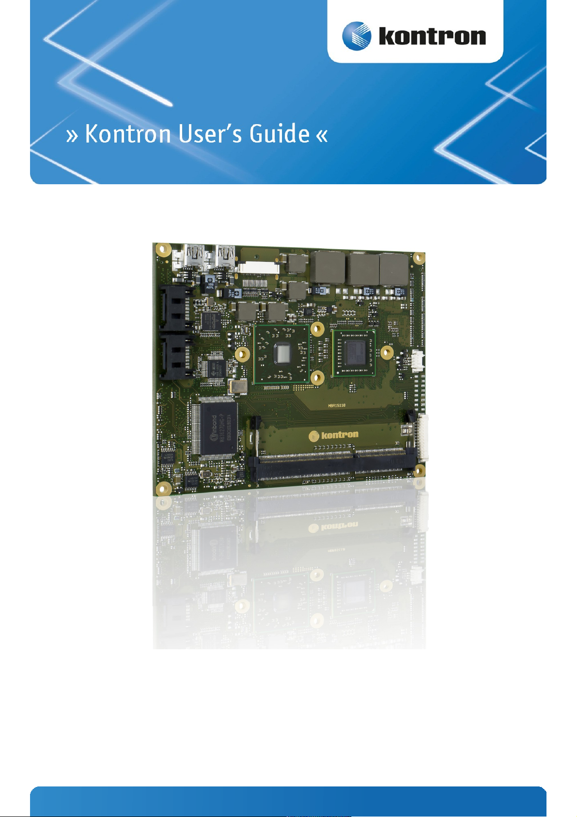
ETX-OH
Document Revision 130
www.kontron.com
Page 2

Page 3

» Table of Contents «
1 User Information..................................................................................5
1.1 About This Document.................................................................................................................... 5
1.2 Copyright Notice.......................................................................................................................... 5
1.3 Trademarks................................................................................................................................. 5
1.4 Standards................................................................................................................................... 5
1.5 Warranty.................................................................................................................................... 6
1.6 Technical Support......................................................................................................................... 6
2 Introduction........................................................................................7
2.1 Product Description...................................................................................................................... 7
2.2 ETX® Documtentation................................................................................................................... 7
2.3 ETX® Benefits.............................................................................................................................. 7
3 Specification.......................................................................................8
3.1 Modules & Accessories................................................................................................................... 8
3.2 Functional Specification................................................................................................................ 9
3.3 Block Diagram............................................................................................................................ 12
3.4 Electrical Specification................................................................................................................ 13
3.4.1 Supply Voltage........................................................................................................................... 13
3.4.2 Power Supply Rise Time................................................................................................................ 13
3.4.3 Supply Voltage Ripple.................................................................................................................. 13
3.4.4 Power Consumption..................................................................................................................... 13
3.5 Environmental Specification......................................................................................................... 14
3.5.1 Temperature Specification............................................................................................................ 14
3.5.2 Humidity................................................................................................................................... 14
3.6 Standards and Certifications.........................................................................................................15
3.7 MTBF........................................................................................................................................ 17
3.8 Mechanical Specification.............................................................................................................. 18
3.9 Module Dimensions..................................................................................................................... 18
3.10 Thermal Management, Heatspreader and Cooling Solutions..................................................................19
3.11 Onboard Connectors....................................................................................................................20
3.11.1 FAN.......................................................................................................................................... 20
3.11.2 SATA........................................................................................................................................ 21
3.11.3 USB......................................................................................................................................... 21
3.11.4 DisplayPort................................................................................................................................ 21
3.11.5 CPU Debug & CPLD....................................................................................................................... 21
4 Features and Interfaces.......................................................................22
4.1 Onboard SSD.............................................................................................................................. 22
4.2 S5 Eco Mode.............................................................................................................................. 23
4.3 M.A.R.S.................................................................................................................................... 24
4.4 Fast I2C.................................................................................................................................... 25
4.5 EAPI, JIDA & PLD Driver................................................................................................................ 26
www.kontron.com
Page 4

ETX-OH /
4.6 K-Tools..................................................................................................................................... 27
4.7 K-Station 2 GUI.......................................................................................................................... 27
4.8 KeAPI....................................................................................................................................... 28
4.9 Watchdog Timer.......................................................................................................................... 29
4.10 C-States.................................................................................................................................... 30
4.11 ACPI Suspend Modes and Resume Events.......................................................................................... 31
5 System Resources...............................................................................32
5.1 Interrupt Request (IRQ) Lines........................................................................................................ 32
5.2 Memory Area............................................................................................................................. 32
5.3 I/O Address Map......................................................................................................................... 33
6 ETX® Connectors................................................................................34
6.1 General Signal Description............................................................................................................ 34
6.2 Connector X1 (PCI bus, USB, Audio)................................................................................................ 35
6.2.1 Connector X1 Signal Levels........................................................................................................... 36
6.3 Connector X2 (ISA Bus)................................................................................................................ 38
6.3.1 Connector X2 Signal Levels........................................................................................................... 39
6.3.2 Connector X3 (Signal Levels)......................................................................................................... 41
6.4 Connector X4 Subsystems............................................................................................................. 43
6.4.1 Connector X4 (IDE 1, IDE 2, Ethernet, Miscellaneous).........................................................................43
6.4.2 Connector X4 (Signal Levels).........................................................................................................44
7 BIOS Operation...................................................................................46
7.1 Determining the BIOS Version....................................................................................................... 46
7.2 BIOS Update.............................................................................................................................. 46
7.3 Setup Guide............................................................................................................................... 48
7.4 POST Codes................................................................................................................................ 48
7.4.1 Start AMI® Aptio Setup Utility....................................................................................................... 48
7.5 BIOS Setup................................................................................................................................ 49
7.5.1 Main........................................................................................................................................ 49
7.5.2 Advanced.................................................................................................................................. 51
7.5.3 Chipset..................................................................................................................................... 83
7.5.4 Boot........................................................................................................................................ 93
7.5.5 Security.................................................................................................................................... 98
7.5.6 Save & Exit................................................................................................................................ 99
4
Page 5

ETX-OH / User Information
1 User Information
1.1 About This Document
This document provides information about products from Kontron Europe GmbH and/or its subsidiaries. No warranty of
suitability, purpose, or fitness is implied. While every attempt has been made to ensure that the information in this
document is accurate, the information contained within is supplied “as-is” and is subject to change without notice.
For the circuits, descriptions and tables indicated, Kontron assumes no responsibility as far as patents or other rights of
third parties are concerned.
1.2 Copyright Notice
Copyright © 2003-2014 Kontron Europe GmbH
All rights reserved. No part of this document may be reproduced, transmitted, transcribed, stored in a retrieval system, or
translated into any language or computer language, in any form or by any means (electronic, mechanical, photocopying,
recording, or otherwise), without the express written permission of Kontron Europe GmbH.
DIMM-PC®, PISA®, ETX®, ETXexpress®, microETXexpress®, X-board®, DIMM-IO® and DIMM-BUS® are trademarks or
registered trademarks of Kontron Europe GmbH. Kontron is trademark or registered trademark of Kontron AG.
1.3 Trademarks
The following lists the trademarks of components used in this board.
» IBM, XT, AT, PS/2 and Personal System/2 are trademarks of International Business Machines Corp.
» Microsoft is a registered trademark of Microsoft Corp.
» Intel is a registered trademark of Intel Corp.
» All other products and trademarks mentioned in this manual are trademarks of their respective owners.
1.4 Standards
Kontron Europe GmbH is certified to ISO 9000 standards.
5
Page 6

ETX-OH / User Information
1.5 Warranty
For this Kontron Europe GmbH product warranty for defects in material and workmanship exists as long as the warranty
period, beginning with the date of shipment, lasts. During the warranty period, Kontron Europe GmbH will decide on its
discretion if defective products are to be repaired or replaced.
Within the warranty period, the repair of products is free of charge as long as warranty conditions are observed.
Warranty does not apply for defects arising/resulting from improper or inadequate maintenance or handling by the buyer,
unauthorized modification or misuse, as well as the operation outside of the product´s environmental specifications and
improper installation and maintenance.
Kontron Europe GmbH will not be responsible for any defects or damages to other products not supplied by Kontron
Europe GmbH that are caused by a faulty Kontron Europe GmbH product.
1.6 Technical Support
Technicians and engineers from Kontron Europe GmbH and/or its subsidiaries are available for technical support. We are
committed to make our product easy to use and will help you use our products in your systems.
Please consult our Website at http://www.kontron.com/support for the latest product documentation, utilities, drivers
and support contacts. Consult our customer section http://emdcustomersection.kontron.com for the latest BIOS
downloads, Product Change Notifications, Board Support Packages, DemoImages, 3D drawings and additional tools and
software. In any case you can always contact your board supplier for technical support.
6
Page 7

ETX-OH / Introduction
2 Introduction
2.1 Product Description
Kontron's ETX®-OH extends availabiltiy and reliability of the established form factor ETX®. It is a successor product for
existing ETX® designs. ETX®-OH raises your investment protection for your ETX® designs.
This Computer-on-Module is populated with AMD's Fusion technology and brings new graphic performance for
userfriendly interfaces or HD video onto your designs.
2.2 ETX® Documtentation
This product manual serves as one of three principal references for an ETX® design. It documents the specifications and
features of ETX®-CD. The other two references, which are available from the Kontron Europe GmbH Web site, include:
» The ETX® Specification defines the ETX® module form factor, pinout, and signals.
» The ETX® Design Guide serves as a general guide for baseboard design, with a focus on maximum flexibility to
accommodate a wide range of ETX® modules.
Some of the information contained within this product manual applies only to certain
product revisions (CE: xxx). If certain information applies to specific product revisions (CE:
xxx) it will be stated. Please check the product revision of your module to see if this
information is applicable.
2.3 ETX® Benefits
Embedded technology extended (ETX) modules are very compact (114 x 95 mm), highly integrated computers. All ETX®
modules feature a standardized form factor and a standardized connector layout that carry a specified set of signals. This
standardization allows designers to create a single-system baseboard that can accept present and future ETX® modules.
ETX® modules include common personal computer (PC) peripheral functions such as:
» Graphics
» Parallel, Serial, and USB ports
» Keyboard/mouse
» Ethernet
» Sound
» IDE (and SATA)
The baseboard designer can optimize exactly how each of these functions implements physically. Designers can place
connectors precisely where needed for the application on a baseboard designed to optimally fit a system’s packaging.
Peripheral PCI or ISA buses can be implemented directly on the baseboard rather than on mechanically unwieldy
expansion cards. The ability to build a system on a single baseboard using the computer as one plug-in component
simplifies packaging, eliminates cabling, and significantly reduces system-level cost. A single baseboard design can use a
range of ETX® modules. This flexibility can differentiate products at various price/performance points, or to design future
proof systems that have a builtin upgrade path. The modularity of an ETX® solution also ensures against obsolescence as
computer technology evolves. A properly designed ETX® baseboard can work with several successive generations of ETX®
modules. An ETX® baseboard design has many advantages of a custom, computer-board design but delivers better
obsolescence protection, greatly reduced engineering effort, and faster time to market.
7
Page 8
ETX-OH / Specification
3 Specification
3.1 Modules & Accessories
The Computer-on-Module ETX®-OH (MBR1) based on AMD's Brazos platform is available in different variants to cover the
demand of different performance, price and power:
Commercial grade modules (0°C to 60°C operating)
Product Number Product Name Processor Chipset and Features
18040-0000-16-2 ETX-OH T56N AMD G-Series T56N 2×1.65GHz AMD A55E FCH
18040-0000-16-4 ETX-OH T56E AMD G-Series T56E 2×1.65GHz AMD A55E FCH
18040-0000-10-2 ETX-OH T40E AMD G-Series T40E 2×1.0GHz AMD A55E FCH
18040-0000-15-1 ETX-OH T52R AMD G-Series T52R 1.5GHz AMD A55E FCH
18040-0000-10-1 ETX-OH T40R AMD G-Series T40R 1.0GHz AMD A55E FCH
18040-0000-06-1 ETX-OH T16R AMD G-Series T16R 615MHz AMD A55E FCH
Extended temperature modules (E1, -25°C to 75°C operating)
Product Number Product Name Processor Chipset and Features
18040-0000-16-2EXT ETX-OH T56N E1 AMD G-Series T56N 2×1.65GHz AMD A55E FCH, E1
18040-0000-16-4EXT ETX-OH T56E E1 AMD G-Series T56E 2×1.65GHz AMD A55E FCH, E1
18040-0000-10-2EXT ETX-OH T40E E1 AMD G-Series T40E 2×1.0GHz AMD A55E FCH, E1
18040-0000-10-1EXT ETX-OH T40R E1 AMD G-Series T40R 1.0GHz AMD A55E FCH, E1
18040-0000-06-1EXT ETX-OH T16R E1 AMD G-Series T16R 615MHz AMD A55E FCH, E1
Optional hardware features:
» TPM
» DP connector instead of FlatFoil
» Onboard SATA NANDrive
» Onboard miniUSB connector
Accessories
Product Number Carrier Boards
18010-0000-00-0 ETX® Eval
18028-0000-00-0 ETX® miniBaseboard
Product Number Memory
97015-1024-16-0 DDR3-1600 SODIMM 1GB
97015-2048-16-0 DDR3-1600 SODIMM 2GB
97015-4096-16-0 DDR3-1600 SODIMM 4GB
97015-1024-16-2 DDR3-1600 SODIMM 1GB E2
97015-2048-16-2 DDR3-1600 SODIMM 2GB E2
97015-4096-16-2 DDR3-1600 SODIMM 4GB E2
Product Number Cooling & Mounting
18040-0000-99-0 ETX®-OH, Heatspreader, threaded
18040-0000-99-1 ETX®-OH, Heatspreader, through hole
18099-0000-99-0 ETX® Active Uni Cooler (5V FAN)
36099-0000-99-0 COMe Active Uni Cooler (12V FAN)
36099-0000-99-1 COMe Passive Uni Cooler
Product Number Adapter & Cables
96085-0000-00-0 KAB-ADAPT-FF-DP (22pin Flatfoil to DisplayPort adapter cable)
96006-0000-00-8 ADA-DP-LVDS (DP to LVDS converter)
9-5000-0352 ADA-LVDS-DVI 18bit (LVDS to DVI converter)
9-5000-0353 ADA-LVDS-DVI 24bit (LVDS to DVI converter)
96082-0000-00-0 KAB-ADAPT-DP-DVI (DP to DVI adapter cable)
96083-0000-00-0 KAB-ADAPT-DP-VGA (DP to VGA adapter cable)
96084-0000-00-0 KAB-ADAPT-DP-HDMI (DP to HDMI adapter cable)
96079-0000-00-0 KAB-HSP 200mm (Cable adapter to connect FAN to module)
96079-0000-00-2 KAB-HSP 40mm (Cable adapter to connect FAN to module)
8
Page 9
ETX-OH / Specification
3.2 Functional Specification
Processor
The 40nm AMD™ embedded G-Series APU Rev C0 (eOntario) with FT1 (413-BGA) Package CPU supports:
» AMD64
» AMD PowerNow!
» DMX: AMD Digital Media Xpress™ technology (SSE, SSE2, SSE3, SSE4a, MMX instructions)
» AMD-V™: AMD Virtualization™ technology
» EVP: AMD Enhanced Virus Protection
Processor Cores Clock L2 Cache Memory GPU Core GPU Clock (Turbo) AMD Turbo Core Max TDP
AMD G-Series T56N 2 1.65GHz 2x512kB DDR3-1333 Radeon HD6320 500MHz (600MHz) Yes 18W
AMD G-Series T56E 2 1.65GHz 2x512kB DDR3-1333 Radeon HD6250 280MHz No 18W
AMD G-Series T40E 2 1.00GHz 2x512kB DDR3-1066 Radeon HD6250 280MHz No 6.4W
AMD G-Series T52R 1 1.50GHz 512kB DDR3-1333 Radeon HD6310 500MHz No 18W
AMD G-Series T40R 1 1.00GHz 512kB DDR3-1066 Radeon HD6250 280MHz No 5.5W
AMD G-Series T16R 1 615MHz 512kB DDR3-1066 Radeon HD6250 280MHz No 4.5W
Memory
Sockets
1x DDR3 SO-DIMM
Memory Type
DDR3-1066/1333
Maximum Size
4GB
Technology
Single Channel
Graphics Core
The integrated Mobility Radeon HD6320/6310/6250 supports:
» UVD: Unified Video Decoder for hardware decode of high definition video
» 80 Stream Processing Units (SPs)
» 8 Texture Mapping Units (TMUs)
» 4 Raster Operation Processors (ROPs)
Graphics Core Render Clock
HD6320/10: 500MHz (T56N, T52R), HD6250: 280MHz (T40E, T40R, T16R)
Execution Units / Pixel Pipelines
4 with 80 unified shader
Max Graphics Memory
512MB
GFX Memory Bandwidth (GB/s)
17.1
GFX Memory Technology
UMA
API (DirectX/OpenGL)
11 / 4.1 + OCL 1.1
Shader Model
5.0
Hardware accelerated Video
ATI Avivo HD: H.264, VC-1, Blu-ray
Independent/Simultaneous Displays
2
Display Interfaces
CRT max Resolution
2560x1600 / 1920x1200
TV out:
-
Digital Display:
DP++ (FFC22 or optional DP connector)
LVDS
LVDS Bits/Pixel
1x18, 2x18, 1x24, 2x24
LVDS Bits/Pixel with dithering
-
LVDS max Resolution:
1920x1200
PWM Backlight Control:
YES
9
Page 10
ETX-OH / Specification
Chipset & IOH
# of USB:
4x USB 1.1/2.0
USB onboard Connector:
2x miniUSB optional
Audio:
Realtek ALC886GR HDAudio
PCI Bus:
PCI Rev 2.3 (33MHz/3.3V)
ISA Bus:
PCI2ISA ITE8888
SuperI/O Controller
Winbond 83627DHG-P
COM Ports:
2x RS232
IrDA Support:
IrDA 1.0 (SIR) or ASK-IrDA (COM2)
LPT Support:
EPP, ECP, bi-dir.
Max TDP:
4.7W
Storage
Primary IDE:
JMB368 PCIe2PATA
Secondary IDE:
JMB368 PCIe2PATA
SATA onboard connector:
2x SATA 3Gb/s
SATA features:
Raid0/1, NCQ, HotPlug, eSATA
SATA RAID support:
-
onboard SSD:
2-32GB SLC or 2-64GB MLC optional
onboard CF Card:
-
Onboard devices
Audio
Realtek ALC886GR HDAudio
Trusted Platform Module
Infineon TPM 1.2 SLB9635TT optional
Ethernet
The Broadcom BCM54610 ethernet supports:
» Jumbo Frames
» Time Sync Protocol Indicator
» WOL (Wake On LAN)
» PXE (Preboot eXecution Environment)
10
Page 11
ETX-OH / Specification
Kontron Features
I2C/SMB support:
YES/YES
M.A.R.S. support
YES
Embedded API
PICMG EAPI / JIDA32
Custom BIOS Settings / Flash Backup
YES
Watchdog support
YES
Power Features
ACPI
ACPI 3.0
S-States
S0, S3, S4, S5
Graphic States
D0,D3
Misc Power Management
DPST 6.0
Power Consumption and Performance
Full Load Power Consumption
9 - 19.4W
Kontron Performance Index
5920 - 15443
Kontron Performance/Watt
661 - 997
Detailed Power Consumption measurements in all states and bechmarks for CPU, Graphics
and Memory performance are available in Application Note KEMAP054 at EMD Customer
Section.
Supported Operating Systems
The ETX®-OH supports:
» Microsoft Windows CE6
» Microsoft Windows embedded Compact 7 (WEC7)
» Microsoft Windows embedded Standard 7 (WES7)
» Microsoft Windows XP
» Microsoft Windows 7
» Linux
» VxWorks
11
Page 12
ETX-OH / Specification
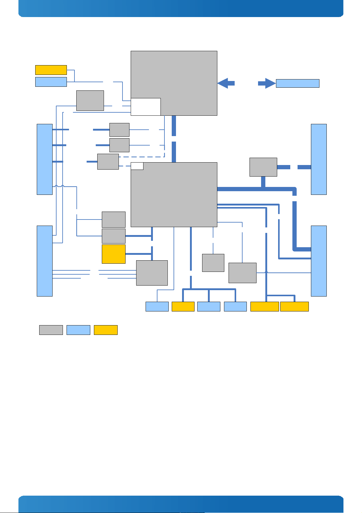
3.3 Block Diagram
12
0
4xUMI
AMD Fusion APU
Embedded G-Series
Processor (eOntario)
SC/DC 5-18W
X3
280MHz Radeon
HD6250
500MHz Radeon
HD6310
HDA
Codec
ALC886GR
I2C
VGA
LPT
PS/2
COM1/COM2
HDA
PCI
ISA
LPC
SPI
USB 0-3
FAN
Connector
Primary IDE
DDR3-SODIMM
DDR3-1066
DDR3-1333
EEPROM
(CMOS
Setup Data)
USB 4/5
miniUSB
Connector
SATA
PCIe
TPM
Infineon
SLB9655TT
PCIe
PCI to ISA
Bridge
ITE8888
X1
X2
EC
fastI2C,
sWD
SATA
Connector
Hudson-E1 A55E
Fusion Controller Hub FCH
Super I/O
Controller
Winbond
W83627DHG-P
5 1
Secondary IDE
SPI
BIOS
Flash
PCIe to
PATA
JMB368
PCIe to
PATA
JMB368
SATA
Connector
miniUSB
Connector
DDI0
DPtoLVDS
Analogix
ANX3110
2x18/24
LVDS
DisplayPort
Connector
DDI1
SATA SSD
10/100 LAN
Ethernet
Contr.
X4
MAC
DisplayPort
Flatfoil
Connector Option
Standard
component
Page 13

ETX-OH / Specification
3.4 Electrical Specification
3.4.1 Supply Voltage
Following supply voltage is specified at the ETX® connector:
Supply Voltage:
5V +/- 5%
5V_Stb:
5V DC +/- 5%
3.4.2 Power Supply Rise Time
» The input voltages shall rise from ≤10% of nominal to within the regulation ranges within 0.1ms to 20ms.
» There must be a smooth and continuous ramp of each DC input voltage from 10% to 90% of its final set-point
following the ATX specification
3.4.3 Supply Voltage Ripple
» Maximum 100 mV peak to peak 0 – 20 MHz
3.4.4 Power Consumption
The maximum Power Consumption of the different ETX®-OH modules is 9 - 19.4W (100% CPU load; 90°C CPU
temperature). Further details with measurements and TDP values of the single variants can be found in our customer
section. Information there is available after registration.
13
Page 14
ETX-OH / Specification
3.5 Environmental Specification
3.5.1 Temperature Specification
Kontron defines following temperature grades for Computer-on-Modules in general. Please see chapter 'Product
Specification' for available temperature grades for the ETX®-OH
Temperature Specification Operating Non-operating Validated Input Voltage
Commercial grade 0°C to +60°C -30°C to +85°C VCC:
Extended Temperature (E1) -25°C to +75°C -30°C to +85°C VCC: 12V
Industrial grade by Screening (XT)
-40°C to +85°C -40°C to +85°C VCC: 12V
Industrial grade by Design (E2)
-40°C to +85°C -40°C to +85°C VCC:
Operating with Kontron heatspreader plate assembly
The operating temperature defines two requirements:
» the maximum ambient temperature with ambient being the air surrounding the module.
» the maximum measurable temperature on any spot on the heatspreader's surface
Test specification:
Temperature Grade Validation requirements
Commercial grade at 60°C HSP temperature the CPU @ 100% load needs to run at nominal frequency
Extended Temperature (E1) at 75°C HSP temperature the CPU @ 75% load is allowed to start speedstepping for thermal protection
Industrial grade by Screening (XT)
at 85°C HSP temperature the CPU @ 50% load is allowed to start throttling for thermal protection
Industrial grade by Design (E2)
at 85°C HSP temperature the CPU @ 50% load is allowed to start throttling for thermal protection
Operating without Kontron heatspreader plate assembly
The operating temperature is the maximum measurable temperature on any spot on the module's surface.
3.5.2 Humidity
» 93% relative Humidity at 40°C, non-condensing (according to IEC 60068-2-78)
14
Page 15

ETX-OH / Specification
3.6 Standards and Certifications
RoHS II
The ETX®-OH is compliant to the directive 2011/65/EU on the Restriction of the use of certain Hazardous Substances
(RoHS II) in electrical and electronic equipment
Component Recognition UL 60950-1
The ETX® 3.0 form factor Computer-on-Modules are Recognized by Underwriters Laboratories Inc. Representative
samples of this component have been evaluated by UL and meet applicable UL requirements.
UL Listings:
» NWGQ2.E304278
» NWGQ8.E304278
WEEE Directive
WEEE Directive 2002/96/EC is not applicable for Computer-on-Modules.
Conformal Coating
Conformal Coating is available for Kontron Computer-on-Modules and for validated SO-DIMM memory modules. Please
contact your local sales or support for further details.
15
Page 16

ETX-OH / Specification
Shock & Vibration
The ETX® 3.0 form factor Computer-on-Modules successfully passed shock and vibration tests according to
» IEC/EN 60068-2-6 (Non operating Vibration, sinusoidal, 10Hz-4000Hz, +/-0.15mm, 2g)
» IEC/EN 60068-2-27 (Non operating Shock Test, half-sinusoidal, 11ms, 15g)
EMC
Validated in Kontron reference housing for EMC the ETX®-OH follows the requirements for electromagnetic compatibility
standards
» EN55022
16
Page 17

ETX-OH / Specification
3.7 MTBF
The following MTBF (Mean Time Before Failure) values were calculated using a combination of manufacturer’s test data, if
the data was available, and the Telcordia (Bellcore) issue 2 calculation for the remaining parts.
The calculation method used is “Bellcore Method 1 Case 1” in a ground benign, controlled environment (GB,GC). This
particular method takes into account varying temperature and stress data and the system is assumed to have not been
burned in.
Other environmental stresses (extreme altitude, vibration, salt water exposure, etc) lower MTBF values.
System MTBF (hours): 212866 @ 40°C
Fans usually shipped with Kontron Europe GmbH products have 50,000-hour typical
operating life. The above estimates assume no fan, but a passive heat sinking arrangement
Estimated RTC battery life (as opposed to battery failures) is not accounted for in the above
figures and need to be considered separately. Battery life depends on both temperature
and operating conditions. When the Kontron unit has external power; the only battery
drain is from leakage paths.
17
Page 18
ETX-OH / Specification
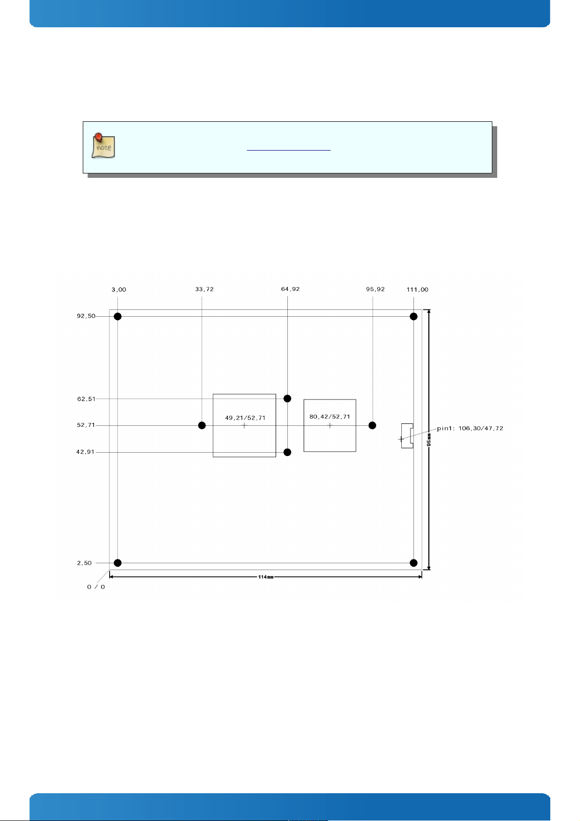
3.8 Mechanical Specification
» 95.0 mm x 114.0 mm
» Hight approx. 12mm (0.4”)
CAD drawings are available at EMD CustomerSection
3.9 Module Dimensions
» Height on Top Standard: 5.50mm (SATA connector)
» Max Height on Top: 6.50mm (DisplayPort connector instead FlatFoil)
» Height on Bottom: 2mm
18
Page 19

ETX-OH / Specification
3.10 Thermal Management, Heatspreader and Cooling Solutions
A heatspreader plate assembly is available from Kontron Europe GmbH for the ETX®-OH. The heatspreader plate on top of
this assembly is NOT a heat sink. It works as a ETX® 3.0-standard thermal interface to use with a heat sink or external
cooling devices.
External cooling must be provided to maintain the heatspreader plate at proper operating temperatures. Under worstcase conditions, the cooling mechanism must maintain an ambient air and heatspreader plate temperature on any spot of
the heatspreader's surface according the module specifications:
» 60°C for commercial grade modules
» 75°C for extended temperature grade modules (E1)
» 85°C for industrial temperature grade modules (E2/XT)
The aluminum slugs and thermal pads or the heat-pipe on the underside of the heatspreader assembly implement thermal
interfaces between the heatspreader plate and the major heat-generating components on the ETX®-OH. About 80 percent
of the power dissipated within the module is conducted to the heatspreader plate and can be removed by the cooling
solution.
You can use many thermal-management solutions with the heatspreader plates, including active and passive approaches.
The optimum cooling solution varies, depending on the ETX® 3.0 application and environmental conditions. Active or
passive cooling solutions provided from Kontron Europe GmbH for the ETX®-OH are usually designed to cover the power
and thermal dissipation for a commercial grade temperature range used in a housing with proper air flow.
Documentation and CAD drawings of ETX®-OH heatspreader and cooling solutions are provided at
http://emdcustomersection.kontron.com.
19
Page 20
ETX-OH / Specification
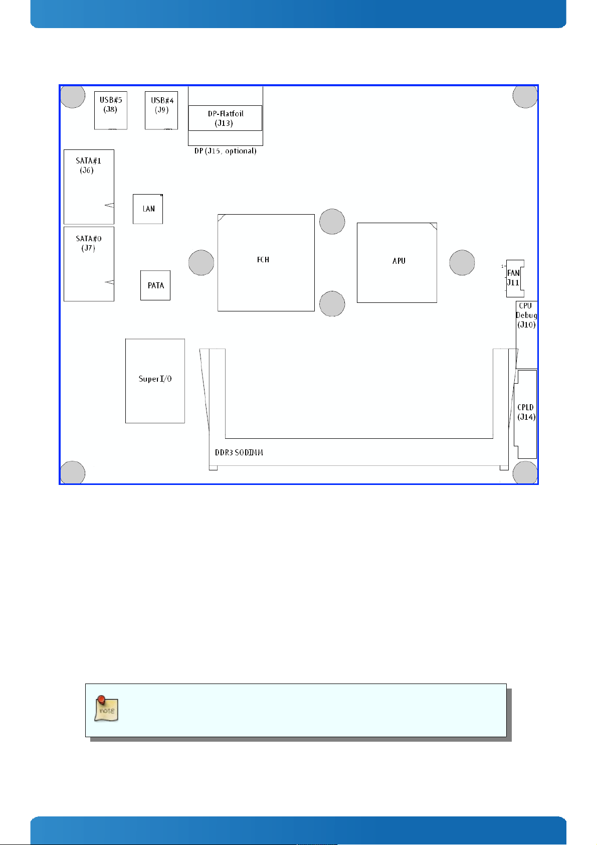
3.11 Onboard Connectors
3.11.1 FAN
With certain BIOS-settings it is possible to control the fan depending on the Active Trip Point temperature. The fan
switches on/off depending on the adjusted Active Trip Point temperature. In order for this feature to function properly an
ACPI compliant OS is necessary.
The onboard fan connector (J11) has following Pin assignment:
» Pin1: Tacho
» Pin2: VCC
» Pin3: GND
Electrical Characteristics
» FAN VCC = 5 V
To connect a standard FAN with 3pin connector to the module please use adaptor cable
KAB-HSP 200mm (96079-0000-00-0) or KAB-HSP 40mm (96079-0000-00-2)
20
Page 21
ETX-OH / Specification
3.11.2 SATA
According the latest ETX® specification 3.0 the ETX®-OH provides two onboard SATA 3Gbps Ports with standard SATA pinout
SATA PIN Signal
1 Ground
2 Transmit+
3 Transmit-
4 Ground
5 Receive-
6 Receive+
7 Ground
3.11.3 USB
The ETX®-OH optionally supports two onboard USB 2.0 Mini-AB connectors J8 & J9. The Mini-AB USB On-The-Go (OTG)
allows additional Hi-Speed USB support for external devives.
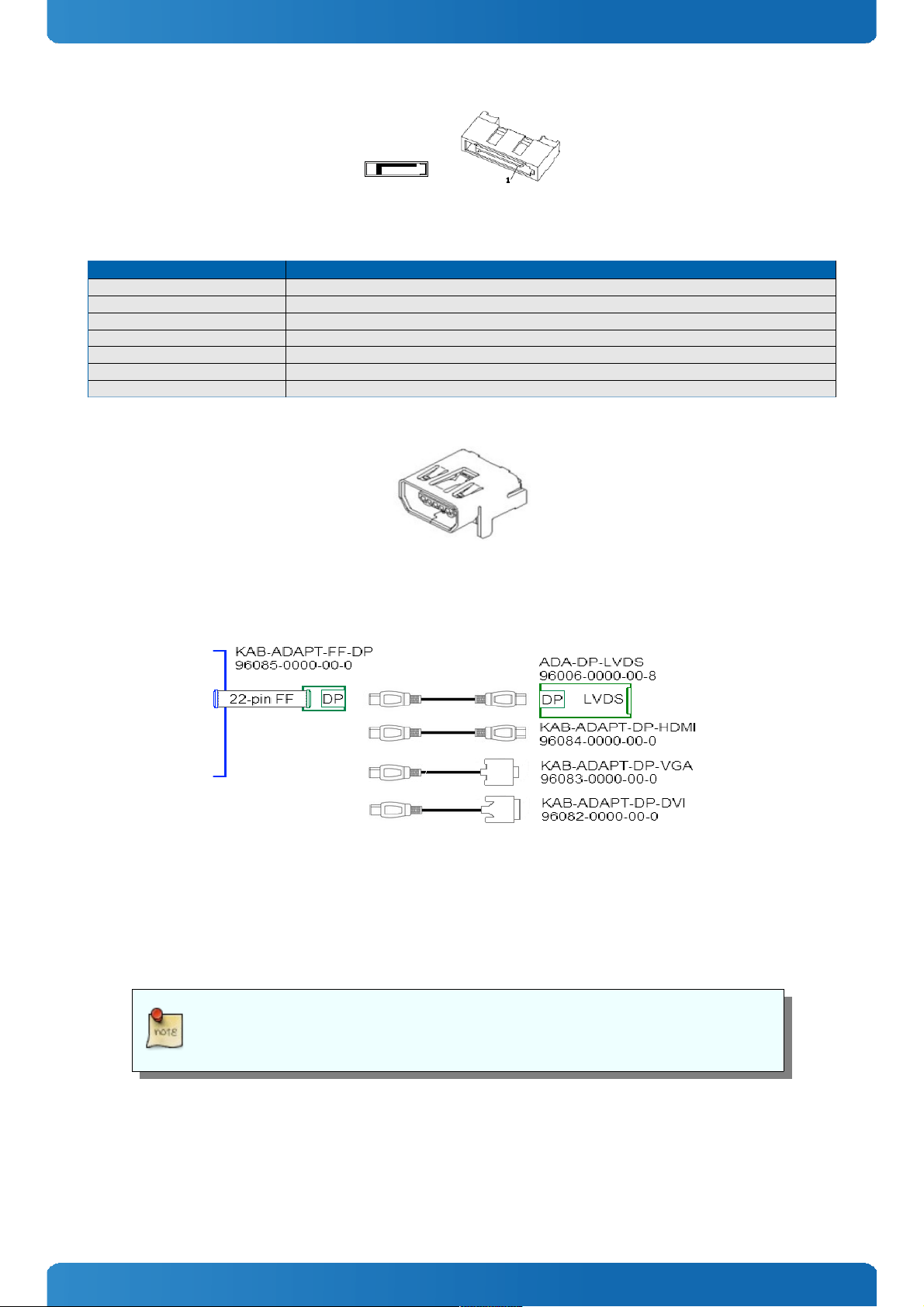
3.11.4 DisplayPort
For external high-resolution displays the ETX®-OH supports an onboard connection for DisplayPort additionally to VGA
and LDVS. By default the module is equipped with the 22-pin FlatFoil solution for best compatibility to existing ETX®
carrier boards without having mechanical connectivity problems. The Flatfoil-to-DisplayPort cable KAB-ADAPT-FF-DP
allows connectivity of standard DisplayPort, HDMI, DVI, VGA or LVDS via the Kontron DisplayPort-to-LVDS Konverter:
Alternatively, a combination shape allows the usage of a standard DisplayPort connector (J15) instead of the 22-pin
Flatfoil directly on the module.
Please contact your local sales or support for customized variants with mini USB ports or
DisplayPort
3.11.5 CPU Debug & CPLD
The CPU Debug connector J10 and the CPLD programming interface J14 are for internal use only and should not be used.
21
Page 22
ETX-OH / Features and Interfaces
4 Features and Interfaces
4.1 Onboard SSD
The ETX®-OH features an onboard Greenliant SATA NAND flash drive with capacities of 2-32GB SLC or 2-64GB MLC
optional. Due to performance and longevity reasons standard variants with onboard flash use SLC type only. The following
SATA NANDrives are available:
Basic features of the SATA NANDrives
» ATA/ATAPI-8 compliant Host interface with 48-bit address feature set and SMART support
» RoHS compliant NAND flash type
» SATA 1.5Gb/s Host transfer rate
» Hardware error detection, correction ECC and advanced wear leveling
» Bad block management
» TRIM support
» SMART support
» 0°C to +70°C temperature range for MLC types A-M-C/B-M-C
» -40°C to +85°C temperature range for MLC types B-M-I
» -40°C to +85°C temperature range for all SLC types
Single-level Cell (SLC) NANDrive™
Flash Part No. GLS85LS
Flash Part No. 1002P-S-I-FZJE-ND104 1004P-S-I-FZJE-ND104 1008P-S-I-FZJE-ND104 1016P-S-I-FZJE-ND104 1032P-S-I-FZJE-ND104
Product Revision
CC1 CC1 CC1 CC1 CC1
Flash Size 2GByte 4GByte 8GByte 16GByte 32GByte
Burst Read/Write Speed
35/20 MB/s 70/35 MB/s 70/50 MB/s 70/55 MB/s 120/80 MB/s
Total Bytes
2,000,388,096 4,001,292,288 8,012,390,400 16,013,942,784 32,017,047,552
Active Mode Power
450mW 560mW 750mW 590mW 855mW
Typical P/E Cycles per
block
100,000 100,000 60,000 60,000 60,000
(Data based on Datasheet S71432 Rev. 03.100 from 11-2013 and S71445 Rev. 01.400 from 11-2013)
Multi-level Cell (MLC) NANDrive™
Flash Part No. GLS85LS
Flash Part No. 1002A-M-C-FZJE-
ND103
1002A-M-I-FZJEND103
1004A-M-C-FZJEND103
1004A-M-I-FZJEND103
1008B-M-C-FZJEND103
1008B-M-I-FZJEND103
1016B-M-C-FZJEND103
1016B-M-I-FZJEND103
1032B-M-C-FZJEND103
1032B-M-I-FZJEND103
1064B-M-C-FZJEND103
1064B-M-I-FZJEND103
Product Revision
CB2 CB2 CB2 CB2 CB2 CB2
Flash Size 2GByte 4GByte 8GByte 16GByte 32GByte 64GByte
Burst Read/Write
Speed
35/10 MB/s 35/10 MB/s 35/10 MB/s 70/20 MB/s 70/30 MB/s 110/60 MB/s
Total Bytes
1,941,553,152 3,941,941,248 8,012,390,400 16,013,942,784 32,017,047,552 64,023,257,088
Active Mode Power
360mW 360mW 360mW 440mW 565mW 820mW
Typical P/E Cycles per
block
5,000 5,000 5,000 5,000 5,000 5,000
(Data based on Datasheet S71430 Rev 02.00 from 10-2013)
22
Page 23

ETX-OH / Features and Interfaces
4.2 S5 Eco Mode
Kontron’s new high-efficient power-off state S5 Eco enables lowest power-consumption in soft-off state – less than 1 mA
compared to the regular S5 state this means a reduction by at least factor 200!
In the “normal” S5 mode the board is supplied by 5V_Stb and needs usually up to 300mA just to stay off. This mode allows
to be switched on by power button, RTC event and WakeOnLan, even when it is not necessary. The new S5 Eco mode
reduces the current enormous.
The S5 Eco Mode can be enabled in BIOS Setup, when the BIOS supports this feature.
Following prerequisites and consequences occur when S5 Eco Mode is enabled
» The power button must be pressed at least for 200ms to switch on.
» Wake via Power button only.
» “Power On After Power Fail”/“State after G3”: only “stay off” is possible
23
Page 24

ETX-OH / Features and Interfaces
4.3 M.A.R.S.
The Smart Battery implementation for Kontron Computer-on-Modules called Mobile Application for Rechargeable Systems
is a BIOS extension for external Smart Battery Manager or Charger. It includes support for SMBus charger/selector (e.g.
Linear Technology LTC1760 Dual Smart Battery System Manager) and provides ACPI compatibility to report battery
information to the Operating System.
Reserved SM-Bus addresses for Smart Battery Solutions on the carrier:
8-bit Address 7-bit Address Device
12h 0x09 SMART_CHARGER
14h 0x0A SMART_SELECTOR
16h 0x0B SMART_BATTERY
24
Page 25

ETX-OH / Features and Interfaces
4.4 Fast I2C
The ETX®-OH supports a CPLD implemented LPC to I2C bridge using the WISHBONE I2C Master Core provided from
opencores.org. The I2C Interface supports transfer rates up to 40kB/s and can be configured in Setup
Specification for external I2C:
» Speed up to 400kHz
» Compatible to Philips I2C bus standard
» Multi-Master capable
» Clock stretching support and wait state generation
» Interrupt or bit-polling driven byte-by-byte data-transfers
» Arbitration lost interrupt with automatic transfer cancellation
» Start/Stop signal generation/detection
» Bus busy detection
» 7bit and 10bit addressing
25
Page 26
ETX-OH / Features and Interfaces
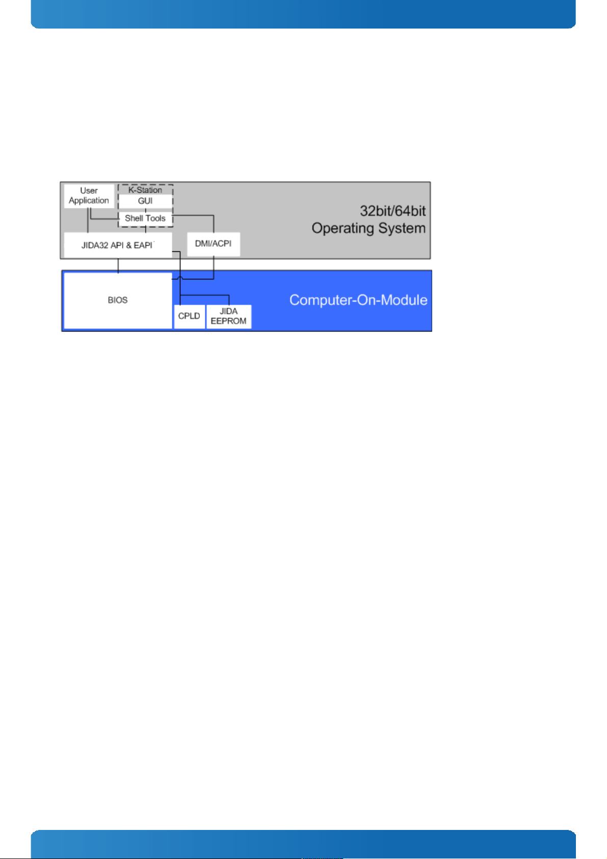
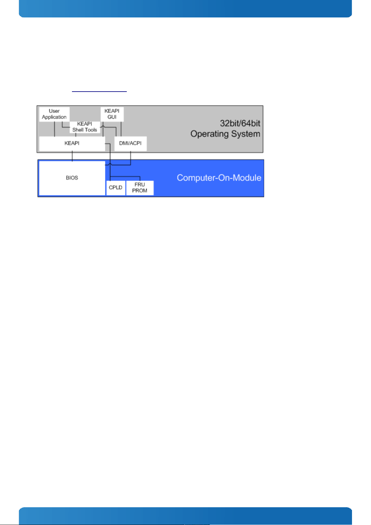
4.5 EAPI, JIDA & PLD Driver
K-Station 2 including the Kontron PLD / Board Driver for new generation modules with UEFI is a replacement for former
JIDA16/JIDA32 BIOS implementations. It consists of hardware drivers providing access to features like Watchdog, I2C Bus
or GPIO implemented in the onboard Programmable Logic Device (CPLD). The Board Driver supports the official PICMG
embedded API (EAPI) and for backwards compatibility the former used Kontron JIDA32 API. The driver (Cpld.sys) and API
(Eapi.dll/Jida.dll) is available for Windows and for Linux.
Usage Model
26
Page 27

ETX-OH / Features and Interfaces
4.6 K-Tools
For easy access to the API Kontron provides Windows Shell Utilities, the so called K-Tools, for direct access to the JIDA32
interface via the Windows command line.
Available K-Station 2 Shell Tools:
» KEthernet.exe (LAN Information)
» KGenInfo.exe (Module Information)
» KHWMon.exe (Hardware Monitoring)
» KI2CBus.exe (I2C and SMBus access)
» KIOPort.exe (GPIO control)
» KStorage.exe (JIDA EEPROM access to user bytes)
» KSystemSummary.exe (System Information)
» KVGATool.exe (LVDS Backlight control)
» KWDog.exe (Watchdog control)
K-Station 2 is available on EMD Customer Section. The Installer allows following installation methods:
» Light Target Installation for JIDA32 and EAPI driver only
» Medium Target Installation for JIDA32 and EAPI with K-Tools
» Host Installation with Sources and Documentation
For silent installation use command
» msiexec /quiet /i K-Station_2xxx_xxx.msi
4.7 K-Station 2 GUI
As an example utility Kontron provides the K-Station 2 GUI for 32 and 64bit Windows. K-Station 2 GUI is a JAVA based
example Graphical User Interface using the K-Tools in Remote Mode. It allows easy and fast evaluation of board specific
features supported by the API and PLD Driver.
27
Page 28
ETX-OH / Features and Interfaces
4.8 KeAPI
The Kontron embedded API (KeAPI) is an extension of the PICMG EAPI mainly with additional remote functionality. It
consists of hardware drivers providing access to features like Watchdog, I2C Bus or GPIO and a QT based user interface
KEAPI GUI. KeAPI is part of standard BSPs for modules based on AMI APTIO (UEFI).
Please refer to EMD Customer Section for detailed documentation and downloads.
Usage of KeAPI
28
Page 29

ETX-OH / Features and Interfaces
4.9 Watchdog Timer
You can configure the Watchdog Timer (WDT) in BIOS setup to start after a set amount of time after power-on boot. The
WDT can also be controlled by the JIDA32 Library API. The application software should strobe the WDT to prevent its
timeout. Upon timeout, the WDT resets and restarts the system. This provides a way to recover from program crashes or
lockups.
Configuration
You can program the timeout period for the watchdog timer in two ranges:
» 1-second increments from 1 to 255 seconds
» 1-minute increments from 1 to 255 minutes
Contact Kontron Embedded Modules technical support for information on programming and operating the WDT.
29
Page 30

ETX-OH / Features and Interfaces
4.10 C-States
New generation platforms include power saving features like SuperLFM, EIST (P-States) or C-States in O/S idle mode.
Activated C-States are able to dramatically decrease power consumption in idle mode by reducing the Core Voltage or
switching of parts of the CPU Core, the Core Clocks or the CPU Cache.
Following C-States are defined:
C-State Description Function
C0 Operating CPU fully turned on
C1 Halt State Stops CPU main internal clocks via sof tware
C1E Enhanced Halt Similar to C1, additionally reduces CPU voltage
C2 Stop Grant Stops CPU internal and external clocks via hardware
C2E Extended Stop Grant Similar to C2, additionally reduces CPU voltage
C3 Deep Sleep Stops all CPU internal and external clock s
C3E Extended Stop Grant Similar to C3, additionally reduces CPU voltage
C4 Deeper Sleep Reduces CPU voltage
C4E Enhanced Deeper Sleep Reduces CPU voltage even more and turns off the memory cache
C6 Deep Power Down Reduces the CPU internal voltage to any value, including 0V
C7 Deep Power Down Similar to C6, additionally LLC (LastLevelCache) is switched off
C-States are usually enabled by default for low power consumption, but active C-States my influence performance
sensitive applications or real-time systems.
» Active C6-State may influence data transfer on external Serial Ports
» Active C7-State may cause lower CPU and Graphics performance
It's recommended to disable C-States / Enhanced C-States in BIOS Setup if any problems occur.
30
Page 31

ETX-OH / Features and Interfaces
4.11 ACPI Suspend Modes and Resume Events
The ETX®-OH supports the S-states S0, S3, S4, S5. S5eco Support: -
The following events resume the system from S3:
» USB Keyboard (1)
» USB Mouse (1)
» Power Button
» WakeOnLan (2)
The following events resume the system from S4:
» Power Button
» WakeOnLan (2)
The following events resume the system from S5:
» Power Button
» WakeOnLan (2)
The following events resume the system from S5Eco:
» Power Button
(1) OS must support wake up via USB devices and baseboard must power the USB Port with
StBy-Voltage
(2) Depending on the Used Ethernet MAC/Phy WakeOnLan must be enabled in BIOS setup
and driver options
31
Page 32

ETX-OH / System Resources
5 System Resources
5.1 Interrupt Request (IRQ) Lines
IRQ # Used For Available Comment
0 Timer0 No -
1 Keyboard No -
2 Cascade No -
3 COM2 Dynamic Onboard SIO (Note 1)
4 COM1 Dynamic Onboard SIO (Note 1)
5 - YES -
6 FDC Dynamic Onboard SIO (Note 1)
7 LPT Dynamic Onboard SIO (Note 1)
8 RTC No -
9 ACPI No -
10 COM4 Dynamic External SIO (Note 1)
11 COM3 Dynamic External SIO (Note 1)
12 PS/2 Mouse No -
13 FPU No -
14 ATA Channel 0 No Note (3)
15 ATA Channel 1 No Note (3)
16 LNK A No PCIe RP 0 + HDAudio + PATA Ch#0; Note(4)
17 LNK B No PCIe RP 1 + USB EHCI (#1 #2 #3)+ PATA Ch#1 + SATA Legacy IDE; Note(4)
18 LNK C No AMD Radeon GFX + USB OHCI (#1 #2 #3 #4) + GbE; Note(4)
19 LNK D No SATA + HD Audio; Note(4)
20 LNK E Yes PCI INTA Note(4)
21 LNK F Yes PCI INTB Note(4)
22 LNK G Yes PCI INTC Note(4)
23 LNK H Yes PCI INTD Note(4)
(1) If the “Used For” device is disabled in setup, the corresponding interrupt is available
for other device.
(2) Only one of the two devices can be used at the same time as they share pins.
(3) Unavailable in SATA legacy mode.
(4) ACPI OS decides on particular IRQ usage
5.2 Memory Area
Upper Memory Used for Available Comment
A0000h – BFFFFh VGA Memory No Mainly used by graphic controller
C0000h – CFFFFh VGA BIOS No Used by onboard VGA ROM
E0000h – FFFFFh System BIOS No Fixed
B8000000h-CFFFFFFFh System No Fixed
D0000000h-DFFFFFFFh AMD Radeon GFX No Fixed
D0000000h–FEBFFFFFh PCIe Conf ig Space No Fixed
FEC00000h-FEC000EFh IOxAPIC No Fixed
FEC000F0h-FEC00FFFh System No Fixed
FEC100F0h-FEC10FFFh System No Fixed
FED00000h-FED003FFh HPET No Fixed
FED00400h-FED00FFFh System No Fixed
FED40000h FED44FFFh TPM No Fixed
FED45000h FED8FFFFh TPM No Fixed
FED61000h-FED70FFFh System No Fixed
FED80000h-FED80FFFh System No Fixed
FEE00000h-FEE00FFFh System No Fixed
FFC00000h-FFFFFFFFh BIOS Flash No Fixed
32
Page 33

ETX-OH / System Resources
5.3 I/O Address Map
The I/O-port addresses of the are functionally identical to a standard PC/AT. All addresses not mentioned in this table
should be available. We recommend that you do not use I/O addresses below 0100h with additional hardware for
compatibility reasons, even if available.
I/O Address Used for Available Comment
0000 - 001F System Ressources No Fixed
0020 - 0021 Interrupt Controller 1 No Fixed
0022 - 003F System Ressources No Fixed
002E - 002F SIO No Fixed
0040 - 0043 Timer, Counter No Fixed
0044 - 005F System Ressources No Fixed
004E - 004F TPM No Fixed
0060 - 0060 Keyboard controller No Fixed
0061 - 0061 System Speaker No Fixed
0062 - 0063 System Ressources No Fixed
0064 - 0064 Keyboard controller No Fixed
0065 - 006F System Ressources No Fixed
0070 - 007F RTC and CMOS Registers No Fixed
0080 BIOS Postcode No Fixed
0081 - 009F DMA Controller No Fixed
00A0 - 00BF Interrupt Controller No Fixed
00C0 - 00DF DMA Controller No Fixed
00E0 - 00EF System Ressources No Fixed
00F0 - 00FF Math Coprocessor No Fixed
0290 - 029F SIO No Fixed
02E8 - 02EF External SIO COM4 Not with ext. SIO Fixed
03B0 - 03DF VGA No Fixed
03E8 - 03EF External SIO COM3 Not with ext. SIO Fixed
040B - 040B Chipset No Fixed
04D0 - 04D1 Chipset No Fixed
04D6 - 04D6 Chipset No Fixed
0800 - 089F Chipset No Fixed
0900 - 090F Chipset No Fixed
0910 - 091F Chipset No Fixed
0B20 - 0B3F Chipset No Fixed
0C00 - 0C01 Chipset No Fixed
0C14 Chipset No Fixed
0C50 - 0C52 Chipset No Fixed
0C6C Chipset No Fixed
0C6F Chipset No Fixed
0CD0 - 0CDF Chipset No Fixed
33
Page 34

ETX-OH / ETX® Connectors
6 ETX® Connectors
The pinouts for ETX® Interface Connectors X1, X2, X3, and X4 are documented for convenient reference. Please see the
ETX® Specification and ETX® Design Guide for detailed, design-level information.
6.1 General Signal Description
Term Description
IO-3,3 Bi-directional 3,3 V IO-Signal
IO-5 Bi-directional 5 V IO-Signal
I-3,3 3,3 V Input
I-5 5 V Input
O-3,3 3,3 V Output
O-5 5 V Output
PU Pull-Up Resistor
PD Pull-Down Resistor
PWR Power Connection
Nc Not Connected / Reserved
34
Page 35

ETX-OH / ETX® Connectors
6.2 Connector X1 (PCI bus, USB, Audio)
Pin Signal Pin Signal Pin Signal Pin Signal
1 GND 2 GND 51 VCC * 52 VCC *
3 PCICLK3 4 PCICLK4 53 PAR 54 SERR#
5 GND 6 GND 55 GPERR# 56 RESERVED
7 PCICLK1 8 PCICLK2 57 PME# 58 USB2#
9 REQ3# 10 GNT3# 59 LOCK# 60 DEVSEL#
11 GNT2# 12 3V 61 TRDY# 62 USB3#
13 REQ2# 14 GNT1# 63 IRDY# 64 STOP#
15 REQ1# 16 3V 65 FRAME# 66 USB2
17 GNT0# 18 RESERVED 67 GND 68 GND
19 VCC * 20 VCC * 69 AD16 70 CBE2#
21 SERIRQ 22 REQ0# 71 AD17 72 USB3
23 AD0 24 3V 73 AD19 74 AD18
25 AD1 26 AD2 75 AD20 76 USB0#
27 AD4 28 AD3 77 AD22 78 AD21
29 AD6 30 AD5 79 AD23 80 USB1#
31 CBE0# 32 AD7 81 AD24 82 CBE3#
33 AD8 34 AD9 83 VCC * 84 VCC *
35 GND 36 GND 85 AD25 86 AD26
37 AD10 38 AUXAL 87 AD28 88 USB0
39 AD11 40 MIC 89 AD27 90 AD29
41 AD12 42 AUXAR 91 AD30 92 USB1
43 AD13 44 ASVCC 93 PCIRST# 94 AD31
45 AD14 46 SNDL 95 INTC# 96 INTD#
47 AD15 48 ASGND 97 INTA# 98 INTB#
49 CBE1# 50 SNDR 99 GND 100 GND
* To protect external power lines of peripheral devices, make sure that:
- the wires have the right diameter to withstand the maximum available current
- the enclosure of the peripheral device fulfils the fire-protection requirements of
IEC/EN60950
35
Page 36

ETX-OH / ETX® Connectors
6.2.1 Connector X1 Signal Levels
Pin Signal Descr iption Type Termination Comment
1 GND Ground PWR - -
2 GND Ground PWR - -
3 PCICLK3 PCI Clock Slot 3 O-3,3 - -
4 PCICLK4 PCI Clock Slot 4 O-3,3 - -
5 GND Ground PWR - -
6 GND Ground PWR - -
7 PCICLK1 PCI Clock Slot 1 O-3,3 - -
8 PCICLK2 PCI Clock Slot 2 O-3,3 - -
9 REQ3# PCI Bus Request 3 I-3,3 PU 15k 3.3V 15k Ohm Resistors
10 GNT3# PCI Bus Grant 3 O-3,3 - -
11 GNT2# PCI Bus Grant 2 O-3,3 - -
12 3V Power +3,3V PWR - -
13 REQ2# PCI Bus Request 2 I-3,3 - int. PU 15k in A55E
14 GNT1# PCI Bus Grant 1 O-3,3 - -
15 REQ1# PCI Bus Request 1 I-3,3 - int. PU 15k in A55E
16 3V Power +3,3V PWR - -
17 GNT0# PCI Bus Grant 0 O-3,3 - -
18 nc - nc - Reserved
19 VCC Power +5V PWR - -
20 VCC Power +5V PWR - -
21 SERIRQ Serial Interrupt Reqest IO-3,3 - int. PU 8k2 in A55E
22 REQ0# PCI Bus Request 0 I-3,3 - int. PU 15k in A55E
23 AD0 PCI Adress & Data Bus line IO-3,3 - -
24 3V Power +3,3V PWR - -
25 AD1 PCI Adress & Data Bus line IO-3,3 - -
26 AD2 PCI Adress & Data Bus line IO-3,3 - -
27 AD4 PCI Adress & Data Bus line IO-3,3 - -
28 AD3 PCI Adress & Data Bus line IO-3,3 - -
29 AD6 PCI Adress & Data Bus line IO-3,3 - -
30 AD5 PCI Adress & Data Bus line IO-3,3 - -
31 CBE0# PCI Bus Command and Byte enables 0 IO-3,3 - -
32 AD7 PCI Adress & Data Bus line IO-3,3 - -
33 AD8 PCI Adress & Data Bus line IO-3,3 - -
34 AD9 PCI Adress & Data Bus line IO-3,3 - -
35 GND Ground PWR - -
36 GND Ground PWR - -
37 AD10 PCI Adress & Data Bus line IO-3,3 - -
38 AUXAL Auxiliary Line Input Lef t I - -
39 AD11 PCI Adress & Data Bus line IO-3,3 - -
40 MIC Microphone Input I - -
41 AD12 PCI Adress & Data Bus line IO-3,3 - -
42 AUXAR Auxiliar y Line Input Right I - -
43 AD13 PCI Adress & Data Bus line IO-3,3 - -
44 ASVCC Analog Supply of Sound Controller O-5 - -
45 AD14 PCI Adress & Data Bus line IO-3,3 - -
46 SNDL Audio Out Lef t O - -
47 AD15 PCI Adress & Data Bus line IO-3,3 - -
48 ASGND Analog Ground of Sound Controller PWR - -
49 CBE1# PCI Bus Command and Byte enables 1 IO-3,3 - -
50 SNDR Audio Out Right O - -
51 VCC Power +5V PWR - -
52 VCC Power +5V PWR - -
53 PAR PCI Bus Parity IO-3,3 - -
54 SERR# PCI Bus System Error IO-3,3 - int. PU 8k2 in A55E
55 GPERR# PCI Bus Grant Error IO-3,3 - int. PU 8k2 in A55E
56 nc - nc - Reserved
57 PME# PCI Power Management Event IO-3,3 - int. PU 10k in A55E
58 USB2# USB Data- , Port2 IO-3,3 - -
59 LOCK# PCI Bus Lock IO-3,3 - int. PU 8k2 in A55E
60 DEVSEL# PCI Bus Device Select IO-3,3 - int. PU 8k2 in A55E
61 TRDY# PCI Bus Target Ready IO-3,3 - int. PU 8k2 in A55E
62 USB3# USB Data- , Port3 IO-3,3 - -
63 IRDY# PCI Bus Initiator Ready IO-3,3 - int. PU 8k2 in A55E
64 STOP# PCI Bus Stop IO-3,3 - int. PU 8k2 in A55E
36
Page 37

ETX-OH / ETX® Connectors
65 FRAME# PCI Bus Cycle Frame IO-3,3 - int. PU 8k2 in A55E
66 USB2 USB Data+ , Port2 IO-3,3 - -
67 GND Ground PWR - -
68 GND Ground PWR - -
69 AD16 PCI Adress & Data Bus line IO-3,3 - -
70 CBE2# PCI Bus Command and Byte enables 2 IO-3,3 - -
71 AD17 PCI Adress & Data Bus line IO-3,3 - -
72 USB3 USB Data+ , Port3 IO-3,3 - -
73 AD19 PCI Adress & Data Bus line IO-3,3 - -
74 AD18 PCI Adress & Data Bus line IO-3,3 - -
75 AD20 PCI Adress & Data Bus line IO-3,3 - -
76 USB0# USB Data- , Port0 IO-3,3 - -
77 AD22 PCI Adress & Data Bus line IO-3,3 - -
78 AD21 PCI Adress & Data Bus line IO-3,3 - -
79 AD23 PCI Adress & Data Bus line IO-3,3 - int. PU 15k in A55E
80 USB1# USB Data- , Port1 IO-3,3 - -
81 AD24 PCI Adress & Data Bus line IO-3,3 - int. PU 15k in A55E
82 CBE3# PCI Command and Byte enables 3 IO-3,3 - -
83 VCC Power +5V PWR - -
84 VCC Power +5V PWR - -
85 AD25 PCI Adress & Data Bus line IO-3,3 - -
86 AD26 PCI Adress & Data Bus line IO-3,3 - int. PU 15k in A55E
87 AD28 PCI Adress & Data Bus line IO-3,3 - -
88 USB0 USB Data+ , Port0 IO-3,3 - -
89 AD27 PCI Adress & Data Bus line IO-3,3 - int. PU 15k in A55E
90 AD29 PCI Adress & Data Bus line IO-3,3 - -
91 AD30 PCI Adress & Data Bus line IO-3,3 - -
92 USB1 USB Data+ , Port1 IO-3,3 - -
93 PCIRST# PCI Bus Reset O-3,3 - -
94 AD31 PCI Adress & Data Bus line IO-3,3 - -
95 INTC# PCI BUS Interrupt Request C I-3,3 - int. PU 8k2 in A55E
96 INTD# PCI BUS Interrupt Request D I-3,3 - int. PU 8k2 in A55E
97 INTA# PCI BUS Interrupt Request A I-3,3 - int. PU 8k2 in A55E
98 INTB# PCI BUS Interrupt Request B I-3,3 - int. PU 8k2 in A55E
99 GND Ground PWR - -
100 GND Ground PWR - -
The termination resistors in this table are already mounted on the ETX® board. Please refer
to the design guide for information about additional termination resistors.
PCI-Bus pins are 5V tolerant.
37
Page 38

ETX-OH / ETX® Connectors
6.3 Connector X2 (ISA Bus)
Pin Signal Pin Signal Pin Signal Pin Signal
1 GND 2 GND 51 VCC * 52 VCC 1)
3 SD14 4 SD15 53 SA6 54 IRQ5
5 SD13 6 MASTER# 55 SA7 56 IRQ6
7 SD12 8 DREQ7 57 SA8 58 IRQ7
9 SD11 10 DACK7# 59 SA9 60 SYSCLK
11 SD10 12 DREQ6 61 SA10 62 REFSH#
13 SD9 14 DACK6# 63 SA11 64 DREQ1
15 SD8 16 DREQ5 65 SA12 66 DACK1#
17 MEMW# 18 DACK5# 67 GND 68 GND
19 MEMR# 20 DREQ0 69 SA13 70 DREQ3
21 LA17 22 DACK0# 71 SA14 72 DACK3#
23 LA18 24 IRQ14 73 SA15 74 IOR#
25 LA19 26 IRQ15 75 SA16 76 IOW#
27 LA20 28 IRQ12 77 SA18 78 SA17
29 LA21 30 IRQ11 79 SA19 80 SMEMR#
31 LA22 32 IRQ10 81 IOCHRDY 82 AEN
33 LA23 34 IO16# 83 VCC * 84 VCC *
35 GND 36 GND 85 SD0 86 SMEMW#
37 SBHE# 38 M16# 87 SD2 88 SD1
39 SA0 40 OSC 89 SD3 90 NOWS#
41 SA1 42 BALE 91 DREQ2 92 SD4
43 SA2 44 TC 93 SD5 94 IRQ9 2)
45 SA3 46 DACK2# 95 SD6 96 SD7
47 SA4 48 IRQ3 97 IOCHK# 98 RSTDRV
49 SA5 50 IRQ4 99 GND 100 GND
1) To protect external power lines of peripheral devices, make sure that:
- The wires have the right diameter to withstand the maximum available current.
- The enclosure of the peripheral device fulfils the fire-protection requirements of
IEC/EN60950
2) IRQ9 is used for SCI in ACPI mode. Do not use for legacy ISA devices.
38
Page 39

ETX-OH / ETX® Connectors
6.3.1 Connector X2 Signal Levels
Pin Signal Description Type Termination Comment
1 GND Ground PWR - -
2 GND Ground PWR - -
3 SD14 ISA Data Bus IO-5 PU 8k2 5V -
4 SD15 ISA Data Bus IO-5 PU 8k2 5V -
5 SD13 ISA Data Bus IO-5 PU 8k2 5V -
6 MASTER# ISA 16-Bit Master I-5 PU 330R 5V -
7 SD12 ISA Data Bus IO-5 PU 8k2 5V -
8 DREQ7 ISA DMA Request 7 I-5 PD 8k2 -
9 SD11 ISA Data Bus IO-5 PU 8k2 5V -
10 DACK7# ISA DMA Acknowledge 7 O-5 - -
11 SD10 ISA Data Bus IO-5 PU 8k2 5V -
12 DREQ6 ISA DMA Request 6 I-5 PD 8k2 -
13 SD9 ISA Data Bus IO-5 PU 8k2 5V -
14 DACK6# ISA DMA Acknowledge 6 O-5 - -
15 SD8 ISA Data Bus IO-5 PU 8k2 5V -
16 DREQ5 ISA DMA Request 5 I-5 PD 8k2 -
17 MEMW# ISA Memor y Write IO-5 PU 8k2 5V -
18 DACK5# ISA DMA Acknowledge 5 O-5 - -
19 MEMR# ISA Memory Read IO-5 PU 8k2 5V -
20 DREQ0 ISA DMA Request 0 I-5 PD 8k2 -
21 LA17 ISA Adress Bus (SA17) IO-5 PU 8k2 5V -
22 DACK0# ISA DMA Acknowledge 0 O-5 - -
23 LA18 ISA Adress Bus (SA18) IO-5 PU 8k2 5V -
24 IRQ14 ISA Interrupt Request 14 / ROM Chip Select IO-5 PU 8k2 5V -
25 LA19 ISA Adress Bus (SA19) IO-5 PU 8k2 5V -
26 IRQ15 ISA Interrupt Request 15 I-5 PU 8k2 5V -
27 LA20 ISA Latchable Adress Bus IO-5 - -
28 IRQ12 ISA Interrupt Request 12 I-5 PU 8k2 5V -
29 LA21 ISA Latchable Adress Bus IO-5 - -
30 IRQ11 ISA Interrupt Request 11 I-5 PU 8k2 5V -
31 LA22 ISA Latchable Adress Bus IO-5 - -
32 IRQ10 ISA Interrupt Request 10 I-5 PU 8k2 5V -
33 LA23 ISA Latchable Adress Bus IO-5 - -
34 IO16# ISA 16-Bit I/O Access I-5 PU 330R 5V -
35 GND Ground PWR - -
36 GND Ground PWR - -
37 SBHE# ISA System Byte High Enable IO-5 PU 8k2 5V -
38 M16# ISA 16-Bit Memory Access IO-5 PU 330R 5V -
39 SA0 ISA Adress Bus IO-5 PU 8k2 5V -
40 OSC ISA Oscillator O-3,3 - 14.318MHz
41 SA1 ISA Adress Bus IO-5 PU 8k2 5V -
42 BALE ISA Buf fer Adress Latch Enable IO-5 PD 4k7 -
43 SA2 ISA Adress Bus IO-5 PU 8k2 5V -
44 TC ISA Terminal Count IO-5 PD 4k7 -
45 SA3 ISA Adress Bus IO-5 PU 8k2 5V -
46 DACK2# ISA DMA Acknowledge 2 O-5 - -
47 SA4 ISA Adress Bus IO-5 PU 8k2 5V -
48 IRQ3 ISA Interrupt Request 3 I-5 PU 8k2 5V -
49 SA5 ISA Adress Bus IO-5 PU 8k2 5V -
50 IRQ4 ISA Interrupt Request 4 I-5 PU 8k2 5V -
51 VCC Power +5V PWR - -
52 VCC Power +5V PWR - -
53 SA6 ISA Adress Bus IO-5 PU 8k2 5V -
54 IRQ5 ISA Interrupt Request 5 I-5 PU 8k2 5V -
55 SA7 ISA Adress Bus IO-5 PU 8k2 5V -
56 IRQ6 ISA Interrupt Request 6 I-5 PU 8k2 5V -
57 SA8 ISA Adress Bus IO-5 PU 8k2 5V -
58 IRQ7 ISA Interrupt Request 7 I-5 PU 8k2 5V -
59 SA9 ISA Adress Bus IO-5 PU 8k2 5V -
60 SYSCLK ISA Bus Clock O-5 - 8.25MHz
61 SA10 ISA Adress Bus IO-5 PU 8k2 5V -
62 REFSH# ISA System Refresh Control IO-5 PU 1k 5V -
63 SA11 ISA Adress Bus IO-5 PU 8k2 5V -
64 DREQ1 ISA DMA Request 1 I-5 PD 8k2 -
39
Page 40

ETX-OH / ETX® Connectors
65 SA12 ISA Adress Bus IO-5 PU 8k2 5V -
66 DACK1# ISA DMA Acknowledge 1 O-5 - -
67 GND Ground PWR - -
68 GND Ground PWR - -
69 SA13 ISA Adress Bus IO-5 PU 8k2 5V -
70 DREQ3 ISA DMA Request 3 I-5 PD 8k2 -
71 SA14 ISA Adress Bus IO-5 PU 8k2 5V -
72 DACK3# ISA DMA Acknowledge 3 O-5 - -
73 SA15 ISA Adress Bus IO-5 PU 8k2 5V -
74 IOR# ISA I/O Read IO-5 PU 8k2 5V -
75 SA16 ISA Adress Bus IO-5 PU 8k2 5V -
76 IOW# ISA I/O Write IO-5 PU 8k2 5V -
77 SA18 ISA Adress Bus IO-5 PU 8k2 5V -
78 SA17 ISA Adress Bus IO-5 PU 8k2 5V -
79 SA19 ISA Adress Bus IO-5 PU 8k2 5V -
80 SMEMR# ISA System Memory Read IO-5 PU 8k2 5V -
81 IOCHRDY ISA I/O Channel Ready IO-5 PU 1k 5V -
82 AEN ISA Adress Enable IO-5 PD 4k7 -
83 VCC Power +5V PWR - -
84 VCC Power +5V PWR - -
85 SD0 ISA Data Bus IO-5 PU 8k2 5V -
86 SMEMW# ISA System Memor y Write O-5 PU 8k2 5V -
87 SD2 ISA Data Bus IO-5 PU 8k2 5V -
88 SD1 ISA Data Bus IO-5 PU 8k2 5V -
89 SD3 ISA Data Bus IO-5 PU 8k2 5V -
90 NOWS# ISA No Wait Staits I-5 PU 330R 5V -
91 DREQ2 ISA DMA Request 2 I-5 PD 8k2 -
92 SD4 ISA Data Bus IO-5 PU 8k2 5V -
93 SD5 ISA Data Bus IO-5 PU 8k2 5V -
94 IRQ9 ISA Interrupt Request 9 I-5 PU 8k2 5V -
95 SD6 ISA Data Bus IO-5 PU 8k2 5V -
96 SD7 ISA Data Bus IO-5 PU 8k2 5V -
97 IOCHK# ISA I/O Channel Check I-5 PU 8k2 5V -
98 RSTDRV ISA Reset O-5 - -
99 GND Ground PWR - -
100 GND Ground PWR - -
The termination resistors in this table are already mounted on the ETX® board. Please refer
to the design guide for information about additional termination resistors.
40
Page 41

ETX-OH / ETX® Connectors
6.3.2 Connector X3 (Signal Levels)
Pin Signal Description Type Termination Comment
1 GND Ground PWR - -
2 GND Ground PWR - -
3 R Analog Video Out RGB - Red Channel O - -
4 B Analog Video Out RGB - Blue Channel O - -
5 HSY Horizontal Synchronization Pulse O-5 - -
6 G Analog Video Out RGB - Green Channel O - -
7 VSY Vertical Synchronization Pulse O-5 - -
8 DDCK Display Data Channel Clock IO-5 PU 2k2 5V -
9 DETECT# / nc Panel Hot-Plug Detection nc - Not supported
10 DDDA Display Data Channel Data IO-5 PU 2k2 5V -
11 LCDDO16 LVDS Channel Data O - -
12 LCDDO18 LVDS Channel Data O - -
13 LCDDO17 LVDS Channel Data O - -
14 LCDDO19 LVDS Channel Data O - -
15 GND Ground PWR - -
16 GND Ground PWR - -
17 LCDDO13 LVDS Channel Data O - -
18 LCDDO15 LVDS Channel Data O - -
19 LCDDO12 LVDS Channel Data O - -
20 LCDDO14 LVDS Channel Data O - -
21 GND Ground PWR - -
22 GND Ground PWR - -
23 LCDDO8 LVDS Channel Data O - -
24 LCDDO11 LVDS Channel Data O - -
25 LCDDO9 LVDS Channel Data O - -
26 LCDDO10 LVDS Channel Data O - -
27 GND Ground PWR - -
28 GND Ground PWR - -
29 LCDDO4 LVDS Channel Data O - -
30 LCDDO7 LVDS Channel Data O - -
31 LCDDO5 LVDS Channel Data O - -
32 LCDDO6 LVDS Channel Data O - -
33 GND Ground PWR - -
34 GND Ground PWR - -
35 LCDDO1 LVDS Channel Data O - -
36 LCDDO3 LVDS Channel Data O - -
37 LCDDO0 LVDS Channel Data O - -
38 LCDDO2 LVDS Channel Data O - -
39 VCC Power +5V PWR - -
40 VCC Power +5V PWR - -
41 JILI_DAT JILI I2C Data Signal IO-3,3 PU 2k2 3,3V -
42 LTGIO0 PWM Brightness control for LCD O-3,3 - -
43 JILI_CLK JILI I2C Clock Signal IO-3,3 PU 2k2 3,3V -
44 BLON# Display Backlight On O-3,3 - -
45 BIASON Display Contrast O-3,3 PU 4k7 3,3V Not supported
46 DIGON Display Power On O-3,3 - -
47 COMP Composite Video / SCART Blue nc - Not supported
48 Y S-Video Luminance / SCART Red nc - Not supported
49 SYNC - nc - Not supported
50 C S-Video Chrominance / SCART Green nc - Not suppor ted
51 LPT / FLPY# LPT / Floppy Interface Configuration Input I-3,3 PU 10k 3,3V High: LPT, Low: Floppy
52 nc - nc - Reserved
53 VCC Power +5V PWR - -
54 GND Ground PWR - -
55 STB# LPT Strobe Signal O-3,3 - -
56 AFD# / DENSEL LPT Automatic Feed / Floppy Density Select O-3,3 - -
57 nc - nc - Reserved
58 PD7 LPT Data Bus D7 IO-3,3 - -
59 IRRX Infrared Receive I-3,3 PU 100k 3,3V -
60 ERR# / HDSEL# LPT Error / Floppy Head Select IO-3,3 - -
61 IRTX Infrared Transmit O-3,3 - -
62 PD6 LPT Data Bus D6 IO-3,3 - -
63 RXD2 Data Receive COM2 I-3,3 PU 100k 5V -
64 INIT# / DIR# LPT Initiate / Floppy Direction O-3,3 - -
41
Page 42

ETX-OH / ETX® Connectors
65 GND Ground PWR - -
66 GND Ground PWR - -
67 RTS2# Request to Send COM2 O-3,3 PU 100k 3,3V -
68 PD5 LPT Data Bus D5 IO-3,3 - -
69 DTR2# Data Terminal Ready COM2 O-3,3 PU 100k 3,3V -
70 SLIN# / STEP# LPT Select / Floppy Motor Step O-3,3 - -
71 DCD2# Data Carrier Detect COM2 I-3,3 PU 4k7 5V -
72 PD4 / DSKCHG# LPT Data Bus D4 / Floppy Disk Change IO-3,3 - -
73 DSR2# Data Set Ready COM2 I-3,3 PU 4k7 5V -
74 PD3 / RDATA# LPT Data Bus D3 / Floppy Raw Data Read IO-3,3 - -
75 CTS2# Clear to Send COM2 I-3,3 PU 4k7 5V -
76 PD2 / WP# LPT Data Bus D2 / Floppy Write Protect Signal IO-3,3 - -
77 TXD2 Data Transmit COM2 O-3,3 - Bootstrap PU 1k 3,3V
78 PD1 / TRK0# LPT Dat a Bus D1 / Floppy Track Signal IO-3,3 - -
79 RI2# Ring Indicator COM2 I-3,3 PU 4k7 5V -
80 PD0 / INDEX# LPT Dat a Bus D0 / Floppy Index Signal IO-3,3 - -
81 VCC Power +5V PWR - -
82 VCC Power +5V PWR - -
83 RXD1 Data Receive COM1 I-3,3 PU 100k 3,3V 5V tolerant
84 ACK# / DRV LPT Acknowledge / Floppy Drive Select IO-3,3 - -
85 RTS1# Request to Send COM1 O-3,3 - Bootstrap PU 1k 3,3V
86 BUSY / MOT LPT Busy / Floppy Motor Select IO-3,3 - -
87 DTR1# Data Terminal Ready COM1 O-3,3 - Bootstrap PU 1k 3,3V
88 PE / WDATA# LPT Paper Empty / Floppy Raw Write Data IO-3,3 - -
89 DCD1# Data Carrier Detect COM1 I-3,3 PU 100k 3,3V -
90 SLCT#/WGATE# LPT Power On / Floppy Write Enable IO-3,3 - -
91 DSR1# Data Set Ready COM1 I-3,3 PU 100k 3,3V -
92 MSCLK Mouse Clock I-3,3 PU 4k7 3,3V -
93 CTS1# Clear to Send COM1 I-3,3 PU 100k 3,3V -
94 MSDAT Mouse Data I-3,3 PU 4k7 3,3V -
95 TXD1 Data Transmit COM1 O-3,3 - Bootstrap PU 1k 3,3V
96 KBCLK Keyboard Clock I-3,3 PU 4k7 3,3V -
97 RI1# Ring Indicator COM1 I-3,3 PU 100k 3,3V -
98 KBDAT Keyboard Data I-3,3 PU 4k7 3,3V -
99 GND Ground PWR - -
100 GND Ground PWR - -
The termination resistors in this table are already mounted on the ETX® board. Please refer
to the design guide for information about additional termination resistors.
LPC,Mouse, Keyboard and COM signals are 5V tolerant.
42
Page 43

ETX-OH / ETX® Connectors
6.4 Connector X4 Subsystems
6.4.1 Connector X4 (IDE 1, IDE 2, Ethernet, Miscellaneous)
Pin Signal Pin Signal Pin Signal Pin Signal
1 GND 2 GND 51 SIDE_IOW# 2) 52 PIDE_IOR#
3 5V_SB 4 PWGIN 53 SIDE_DRQ 2) 54 PIDE_IOW#
5 PS_ON 6 SPEAKER 55 SIDE_D15 2) 56 PIDE_DRQ
7 PWRBTN# 8 BATT 57 SIDE_D0 2) 58 PIDE_D15
9 KBINH# 10 LILED# 59 SIDE_D14 2) 60 PIDE_D0
11 RSMRST# 12 ACTLED# 61 SIDE_D1 2) 62 PIDE_D14
13 ROMKBCS# 2) 14 SPEEDLED# 63 SIDE_D13 2) 64 PIDE_D1
15 EXT_PRG 2) 16 I2CLK 65 GND 66 GND
17 VCC 1) 18 VCC 1) 67 SIDE_D2 2) 68 PIDE_D13
19 OVCR# 20 GPCS# 2) 69 SIDE_D12 2) 70 PIDE_D2
21 EXTSMI# 22 I2DAT 71 SIDE_D3 2) 72 PIDE_D12
23 SMBCLK 24 SMBDATA 73 SIDE_D11 2) 74 PIDE_D3
25 SIDE_CS3# 2) 26 RESERVED 75 SIDE_D4 2) 76 PIDE_D11
27 SIDE_CS1# 2) 28 DASP_S 2) 77 SIDE_D10 2) 78 PIDE_D4
29 SIDE_A2 2) 30 PIDE_CS3# 79 SIDE_D5 2) 80 PIDE_D10
31 SIDE_A0 2) 32 PIDE_CS1# 81 VCC 82 VCC 1)
33 GND 34 GND 83 SIDE_D9 2) 84 PIDE_D5
35 PDIAG_S 2) 36 PIDE_A2 85 SIDE_D6 2) 86 PIDE_D9
37 SIDE_A1 2) 38 PIDE_A0 87 SIDE_D8 2) 88 PIDE_D6
39 SIDE_INTRQ 2) 40 PIDE_A1 89 RESERVED 90 RESERVED
41 RESERVED 42 RESERVED 91 RXD# 92 PIDE_D8
43 SIDE_AK# 2) 44 PIDE_INTRQ 93 RXD 94 SIDE_D7
45 SIDE_RDY 2) 46 PIDE_AK# 95 TXD# 96 PIDE_D7
47 SIDE_IOR# 2) 48 PIDE_RDY 97 TXD 98 HDRST#
49 VCC 1) 50 VCC 1) 99 GND 100 GND
43
Page 44

ETX-OH / ETX® Connectors
6.4.2 Connector X4 (Signal Levels)
Pin Signal Description Type Termination Comment
1 GND Ground PWR - -
2 GND Ground PWR - -
3 5V_SB Supply of internal suspend Circuit PWR - -
4 PWGIN Power Good / Reset Input I-3,3 PU 4k7 3,3V_SB 5V tolerant
5 PS_ON Power Supply On O-5 PU 4k7 5V -
6 SPEAKER Speaker Output O-3,3 - -
7 PWRBTN# Power Button I-5 PU 5k 5V -
8 BATT Battery Supply PWR - -
9 KBINH Keyboard Inhibit Control Input nc - Not supported
10 LILED Ethernet Link LED O - Open collector
11 RSMRST# Resume Reset I-3,3 PU 4k7 3,3V 5V tolerant
12 ACTLED Ethernet Activity LED O - Open collector
13 ROMKBCS# - O-5 PU 10k 5V Not supported
14 SPEEDLED Ethernet Speed LED O - Open collector
15 EXT_PRG - nc - Not supported
16 I2CLK I2C Bus Clock O-5 PU 2k2 5V -
17 VCC Power +5V PWR - -
18 VCC Power +5V PWR - -
19 OVCR# Over Current Detect for USB I-3,3 PU 10k 3,3V -
20 GPCS# - O-5 PU 10k 5V Not supported
21 EXTSMI# System Management Interrupt Input I-3,3 PU 4k7 3,3V 5V tolerant
22 I2DAT I2C Bus Dat a IO-5 PU 2k2 5V -
23 SMBCLK SM Bus Clock O-3,3 PU 2k2 3,3V -
24 SMBDATA SM Bus Data IO-3,3 PU 2k2 3,3V -
25 SIDE_CS3# Secondary IDE Chip Select Channel 1 O-3,3 - -
26 SMBALRT# SMB Alert I-3,3 PU 2k2 3,3V -
27 SIDE_CS1# Secondary IDE Chip Select Channel 1 O-3,3 - -
28 DASP_S - nc - Not suppor ted
29 SIDE_A2 Secondary IDE Adress Bus O-3,3 - -
30 PIDE_CS3# Primary IDE Chip Select Channel 1 O-3,3 - -
31 SIDE_A0 Secondary IDE Adress Bus O-3,3 - -
32 PIDE_CS1# Primary IDE Chip Select Channel 0 O-3,3 - -
33 GND Ground PWR - -
34 GND Ground PWR - -
35 PDIAG_S Secondary IDE CBLID# I-3,3 PD 100k -
36 PIDE_A2 Primary IDE Adress Bus O-3,3 - -
37 SIDE_A1 Secondary IDE Adress Bus O-3,3 - -
38 PIDE_A0 Primary IDE Adress Bus O-3,3 - -
39 SIDE_INTRQ Secondary IDE Interrupt Reqeuest I-3,3 PD 10k -
40 PIDE_A1 Primary IDE Adress Bus O-3,3 - -
41 BATLOW# Battery Low I-3,3 PU 4k7 3,3V 5V tolerant
42 GPE1# General Purpose Power Event 1 I-3,3 - 5V tolerant, pin GEVENT5# with int. PU 8k2 in A55E
43 SIDE_AK# Secondar y IDE DMA Acknowledge O-3,3 - -
44 PIDE_INTRQ Primar y IDE Interrupt Reqeuest I-3,3 PD 10k -
45 SIDE_RDY Secondary IDE Ready I-3,3 PU 4k7 3,3V -
46 PIDE_AK# Pr imary IDE DMA Acknowledge O-3,3 - -
47 SIDE_IOR# Secondary IDE IO Read O-3,3 - -
48 PIDE_RDY Primary IDE Ready I-3,3 PU 4k7 3,3V -
49 VCC Power +5V PWR - -
50 VCC Power +5V PWR - -
51 SIDE_IOW# Secondary IDE IO Write O-3,3 - -
52 PIDE_IOR# Primary IDE IO Read O-3,3 - -
53 SIDE_DRQ Secondary IDE DMA Request I-3,3 PD 5k6 -
54 PIDE_IOW# Primary IDE IO Write O-3,3 - -
55 SIDE_D15 Secondar y IDE Data Bus IO-3,3 - -
56 PIDE_DRQ Primary IDE DMA Request I-3,3 PD 5k6 -
57 SIDE_D0 Secondar y IDE Data Bus IO-3,3 - -
58 PIDE_D15 Pr imary IDE Data Bus IO-3,3 - -
59 SIDE_D14 Secondar y IDE Data Bus IO-3,3 - -
60 PIDE_D0 Pr imary IDE Data Bus IO-3,3 - -
61 SIDE_D1 Secondar y IDE Data Bus IO-3,3 - -
62 PIDE_D14 Pr imary IDE Data Bus IO-3,3 - -
63 SIDE_D13 Secondar y IDE Data Bus IO-3,3 - -
64 PIDE_D1 Pr imary IDE Data Bus IO-3,3 - -
44
Page 45

ETX-OH / ETX® Connectors
65 GND Ground PWR - -
66 GND Ground PWR - -
67 SIDE_D2 Secondar y IDE Data Bus IO-3,3 - -
68 PIDE_D13 Pr imary IDE Data Bus IO-3,3 - -
69 SIDE_D12 Secondar y IDE Data Bus IO-3,3 - -
70 PIDE_D2 Pr imary IDE Data Bus IO-3,3 - -
71 SIDE_D3 Secondar y IDE Data Bus IO-3,3 - -
72 PIDE_D12 Pr imary IDE Data Bus IO-3,3 - -
73 SIDE_D11 Secondar y IDE Data Bus IO-3,3 - -
74 PIDE_D3 Pr imary IDE Data Bus IO-3,3 - -
75 SIDE_D4 Secondar y IDE Data Bus IO-3,3 - -
76 PIDE_D11 Pr imary IDE Data Bus IO-3,3 - -
77 SIDE_D10 Secondar y IDE Data Bus IO-3,3 - -
78 PIDE_D4 Pr imary IDE Data Bus IO-3,3 - -
79 SIDE_D5 Secondar y IDE Data Bus IO-3,3 - -
80 PIDE_D10 Pr imary IDE Data Bus IO-3,3 - -
81 VCC Power +5V PWR - -
82 VCC Power +5V PWR - -
83 SIDE_D9 Secondar y IDE Data Bus IO-3,3 - -
84 PIDE_D5 Pr imary IDE Data Bus IO-3,3 - -
85 SIDE_D6 Secondar y IDE Data Bus IO-3,3 - -
86 PIDE_D9 Pr imary IDE Data Bus IO-3,3 - -
87 SIDE_D8 Secondar y IDE Data Bus IO-3,3 - -
88 PIDE_D6 Pr imary IDE Data Bus IO-3,3 - -
89 GPE2# General Purpose Power Event 1 I-3,3 - 5V tolerant, pin RI# with int. PU 8k2 in A55E
90 CBLID_P# Primary IDE CBLID# I-3,3 PD 100k -
91 RXD# Ethernet Receive Differential Signal ( RXD-) I - -
92 PIDE_D8 Pr imary IDE Data Bus IO-3,3 - -
93 RXD Ethernet Receive Differential Signal ( RXD+) I - -
94 SIDE_D7 Secondar y IDE Data Bus IO-3,3 - int. PD in JMB368
95 TXD# Ethernet Transmit Differential Signal (TXD-) O - -
96 PIDE_D7 Pr imary IDE Data Bus IO-3,3 - int. PD in JMB368
97 TXD Ethernet Transmit Differential Signal (TXD+) O - -
98 HDRST# Hard Drive Reset O-3,3 - -
99 GND Ground PWR - -
100 GND Ground PWR - -
The termination resistors in this table are already mounted on the ETX® board. Please refer
to the design guide for information about additional termination resistors.
45
Page 46

ETX-OH / BIOS Operation
7 BIOS Operation
The module is equipped with AMI® Aptio, which is located in an onboard SPI serial flash memory.
7.1 Determining the BIOS Version
The AMI® Aptio version is displayed in the main menu of the setup utility.
» BIOS Vendor: American Megatrends
» Core Version: x.x.x.x
» BIOS Date: mm/dd/yyyy hh:mm:ss
» BIOS Version: MBR1RXXX
7.2 BIOS Update
Kontron provides continuous BIOS updates for Computer-on-Modules. The updates are provided for download on
http://emdcustomersection.kontron.com with a detailed change description within the according Product Change
Notification (PCN). Please register for EMD Customer Section to get access to BIOS downloads and PCN service.
Modules with BIOS Region/Setup only inside the flash can be updated with AFU utilities (usually 1-3MB BIOS binary file
size) directly. Modules with Intel® Management Engine, Ethernet, Flash Descriptor and other options additionally to the
BIOS Region (usually 4-8MB BIOS binary file size) requires a different update process with Intel Flash Utility FPT and a
wrapper to backup and restore configurations and the MAC address. Therefore it is strongly recommended to use the batch
file inside the BIOS download package available on EMD Customer Section.
» Boot the module to DOS/EFI Shell with access to the BIOS image and Firmware Update Utility provided on EMD
Customer Section
» Execute Flash.bat in DOS or Flash.nsh in EFI Shell
Any modification of the update process may damage your module!
46
Page 47

ETX-OH / BIOS Operation
Backup the BIOS / Create a BIOS with custom defaults:
» Change your BIOS settings according your needs
» Save and Exit Setup with option “Save as User Defaults”. Your customized settings are now stored inside the flash in
a second area additional to the manufacturer defaults
» Boot the module to DOS or EFI Shell with access to the update utilities
» Extract the BIOS region including your custom defaults with afuefix64.efi CBIOS.bin /O in EFI Shell or afudos.exe
CBIOS.rom /O in DOS
Now you can clone the BIOS with your customized default settings to other modules or external SPI flashes with above
mention AFU utilites. On modules with Management Engine and Ethernet inside the Flash the same BIOS core version
should already be programmed on the target.
AMI APTIO update utilities for DOS, EFI Shell and Windows are available for free at AMI.com:
http://www.ami.com/support/downloads/amiflash.zip
47
Page 48

ETX-OH / BIOS Operation
7.3 Setup Guide
The Aptio Setup Utility changes system behavior by modifying the Firmware configuration. The setup program uses a
number of menus to make changes and turn features on or off.
Functional keystrokes in POST:
Key Function
DEL
Enter Setup
F2
Enter Setup
F7
Boot Menu
7.4 POST Codes
Important POST codes during boot-up
AB
BIOS Setup
AD
EFI Shell
AE
Windows
7.4.1 Start AMI® Aptio Setup Utility
To start the AMI® BIOS setup utility, press <DEL> or <F2> when the following string appears during bootup.
Press <DEL> to enter Setup
The Info Menu then appears.
The Setup Screen is composed of several sections:
Setup Screen Location Function
Menu Bar Top Lists and selects all top level menus.
Legend Bar Right side Bottom Lists setup navigation keys.
Item Specific Help Window Right side Top Help for selected item.
Menu Window Left Center Selection fields for current menu.
Menu Bar
The menu bar at the top of the window lists different menus. Use the left/right arrow keys to make a selection.
Legend Bar
Use the keys listed in the legend bar on the bottom to make your selections or exit the current menu. The table below
describes the legend keys and their alternates.
Key Function
or Arrow key ← → Select a menu.
or Arrow key ↑ ↓ Select fields in current menu.
<Home> or <End> Move cursor to top or bottom of current window.
<PgUp> or <PgDn> Move cursor to next or previous page.
+/- Change Option
<Enter> Execute command or select submenu.
<F1> General Help window.
<F2> Previous Values
<F3> Load the optimized default conf iguration.
<F4> Save and exit.
<Esc> Exit menu.
Selecting an Item
Use the or key to move the cursor to the field you want. Then use the + and – keys to select a value for that field. The ↑ ↓
Save Value commands in the Exit menu save the values displayed in all the menus.
Displaying Submenus
Use the or key to move the cursor to the submenu you want. Then press <Enter>. A pointer ( ) marks all submenus. ← → ►
48
Page 49

ETX-OH / BIOS Operation
Item Specific Help Window
The Help window on the right side of each menu displays the Help text for the selected item. It updates as you move the
cursor to each field.
General Help Window
Pressing <F1> on a menu brings up the General Help window that describes the legend keys and their alternates. Press
<Esc> to exit the General Help window.
7.5 BIOS Setup
7.5.1 Main
Feature Options Description
System Language
English
Choose the system default language. English supported
only
System Date [mm/dd/yyyy] Set the Date. Use 'Tab' to switch between Date
elements
System Time [hh:mm:ss] Set the Time. Use 'Tab' to switch between Time
elements
49
Page 50

ETX-OH / BIOS Operation
50
Page 51

ETX-OH / BIOS Operation
7.5.2 Advanced
51
Page 52

ETX-OH / BIOS Operation
PCI Subsystem Settings
Feature Options Description
PCI Latency Timer
32 … 248 PCI Bus Clocks
Value to be programmed into PCI Latency Timer Register
VGA Palette Snoop
Disabled
Enabled
Enables or Disables VGA Palette Registers Snooping
PERR# Generation
Disabled
Enabled
Enables or Disables PCI Device to Generate PERR#
SERR# Generation
Disabled
Enabled
52
Page 53

ETX-OH / BIOS Operation
ACPI Settings
Feature Options Description
Enable ACPI Auto Configuration
Disabled
Enabled
Enables or Disables BIOS ACPI Auto Configuration
Enable Hibernation Disabled
Enabled
Enables or Disables System ability to Hibernate (OS/S4
Sleep State)
ACPI Sleep State Suspend Disabled
S3 only (StR)
Select the highest ACPI sleep state the system will enter
when the SUSPEND button is pressed
Lock Legacy Resources
Disabled
Enabled
Enables or Disables Lock of Legacy Resources
S3 Video Repost
Disabled
Enabled
Enable or Disable S3 Video Repost
Critical Trip Point Disabled
60 … 110
The Celsius Temperature of the ACPI Critical Trip Point.
At his Temperature, the ACPI OS shuts the system off
53
Page 54

ETX-OH / BIOS Operation
Trusted Computing
Feature Options Description
TPM Support
Disable
Enable
Enables or Disables BIOS support for security device.
O.S. will not show Security Device. TCG EFI protocol and
INT1A interface will not be available
TPM State
Disabled
Enabled
Enable/Disable Security Device. Note: Your Computer
will reboot during restar t in order to change Sate of the
Device
Pending Operation
None
Enable Take Ownership
Disable Take Ownership
TPM Clear
Schedule an Operation for the Security Device. Note:
Your Computer will reboot during restart in order to
change Sate of the Device
54
Page 55

ETX-OH / BIOS Operation
CPU Configuration
Feature Options Description
PSS Support Disabled Link
Enabled
Enable/disable the generation of ACPI_PPC, _PSS and
_PCI objects
PSTATE Adjustment
PState 0
PState 1
PState 2
Provide to adjust startup P-state level
PPC Adjustment
PState 0
PState 1
PState 2
Provide to adjust _PPC object
NX Mode Disable Link
Enabled
Enable/disable No-execute page protection Function
SVM Mode Disable Link
Enabled
Enable/disable CPU Virtualization
C6 Mode Disable Link
Enabled
Auto
Enable/disable C6
Core Performance Boost
Disabled
Auto
Enable/disable CPB
PSTATE (degraded) PState 0
PState 1
PState 2
Default
Select degraded P-state when HTC is active
HTC Temp. Limit 100 … 60
Default
Select HTC temperature limit (degree Celsius)
HTC Lock
Disabled
Enabled
Select whether HTC register shall be locked (read only)
55
Page 56

ETX-OH / BIOS Operation
Node 0 Information
56
Page 57

ETX-OH / BIOS Operation
Miscellaneous
Feature Options Description
Restore on AC Power Loss Disabled
Power On
Power Off
Last State
Select the module behavior after AC Power Loss
SB Clock Spread Spect
Disabled
Enabled
Enable or Disable Spread Spectrum
57
Page 58

ETX-OH / BIOS Operation
Watchdog
Feature Options Description
Auto-reload
Disabled
Enabled
Enable automatic reload of watchdog timers on timeout
Global Lock
Disabled
Enabled
If set to enabled, all Watchdog registers (except
WD_KICK) become read only until the board is reset
Stage 1 Mode
Disabled
Reset
NMI
SCI
Select Watchdog Action
Stage 1 Timeout 1s
5s
10s
30s
1m
3m
10m
30m
Select Watchdog Timeout value
58
Page 59

ETX-OH / BIOS Operation
Smart Battery Configuration
Feature Options Description
M.A.R.S. Disabled
AUTO
Charger
Manager
Preset M.A.R.S. Smart Battery System mode. System
must be restarted to reflect mode changes
59
Page 60

ETX-OH / BIOS Operation
Battery Information
60
Page 61

ETX-OH / BIOS Operation
SATA Information
Feature Options Description
SATA Port 0
SATA Port 1
SATA Port 2
- Shows the present devices on SATA0/1 = onboard SATA
Ports and SATA4 = optional SSD Flashdrive
61
Page 62

ETX-OH / BIOS Operation
USB Configuration
Feature Options Description
Legacy USB Support
Enabled
Disabled
AUTO
Enables Legacy USB support. AUTO option disables
legacy support if no USB devices are connected.
DISABLE option will keep USB devices available only for
EFI applications.
USB 2.0 Controller Mode
HiSpeed
FullSpeed
Configures the USB 2.0 controller in HiSpeed
(480Mbps) or FullSpeed (12Mbps)
EHCI Hand-off
Disabled
Enabled
This is a workaround for OSes without EHCI hand-off
Support. The EHCI ownership change should be claimed
by EHCI driver
USB Mass Storage Driver Disabled
Enabled
Enable/Disable USB Mass Storage Driver Support
USB transfer time-out 1sec
5sec
10sec
20sec
The time-out value for Control, Bulk and Interrupt
transfers
Device reset time-out 10sec
20sec
30sec
40sec
USB mass storage device Start Unit command time-out
Device power-up delay
AUTO
Manual
Maximum time the device will take before it properly
reports itself to the Host controller. 'AUTO' uses default
value: for a Root port it is 100ms, for a Hub port the
delay is taken from Hub descriptor
Mass Storage Devices
AUTO
Floppy
Forced FDD
Hard Disk
CD-ROM
Mass storage device emulation type
62
Page 63

ETX-OH / BIOS Operation
SMART Settings
Feature Options Description
SMART Self Test
Disabled
Enabled
Run SMART Self Test on all HDDs during Post
63
Page 64

ETX-OH / BIOS Operation
W83627H Super IO Configuration
Floppy Disk Controller Configuration
Feature Options Description
Floppy Disk Controller Enabled
Disabled
Enable or Disable Floppy Disk Controller. Attention: with
ETX Modules you can either select the onboard floppy
disk or parallel port with the corresponding hardware
strap
Change Settings
Auto
IO=3F0h;IRQ=6;DMA=2;
Select an optimal setting for Super IO device
64
Page 65

ETX-OH / BIOS Operation
Serial Port 0 Configuration
Feature Options Description
Serial Port
Enabled
Disabled
Enable or Disable Serial Port (COM)
Change Settings
Auto
IO=3F8h; IRQ=4
IO=3F8h;IRQ=3,4,5,6,7,9,10,11,12
IO=2F8h;IRQ=3,4,5,6,7,9,10,11,12
IO=3E8h;IRQ=3,4,5,6,7,9,10,11,12
IO=2E8h;IRQ=3,4,5,6,7,9,10,11,12
Select an optimal setting for Super IO device
65
Page 66

ETX-OH / BIOS Operation
Serial Port 1 Configuration
Feature Options Description
Serial Port
Enabled
Disabled
Enable or Disable Serial Port (COM)
Change Settings
Auto
IO=2F8h; IRQ=3
IO=3F8h;IRQ=3,4,5,6,7,9,10,11,12
IO=2F8h;IRQ=3,4,5,6,7,9,10,11,12
IO=3E8h;IRQ=3,4,5,6,7,9,10,11,12
IO=2E8h;IRQ=3,4,5,6,7,9,10,11,12
Select an optimal setting for Super IO device
Device Mode
Standard Serial Port Mode
IrDA 1.0 (HP SIR) Mode
ASKIR Mode
Change the Serial Port mode
66
Page 67

ETX-OH / BIOS Operation
Parallel Port Configuration
Feature Options Description
Parallel Port
Enabled
Disabled
Enable or Disable Parallel Port (LPT/LPTE). Attention:
with ETX Modules you can either select the onboard
floppy disk or parallel port with the corresponding
hardware strap
Change Settings
Auto
IO=378h; IRQ=7
IO=378h;IRQ=6,7,9,10,11,12
IO=278h;IRQ=6,7,9,10,11,12
IO=3BCh;IRQ=6,7,9,10,11,12
Select an optimal setting for Super IO device
Device Mode
Standard Printer Mode
EPP Mode
ECP Mode
EPP Mode & ECP Mode
Change the Parallel Port mode
67
Page 68

ETX-OH / BIOS Operation
Module H/W Health Monitor
CPU Fan Configuration
Feature Options Description
CPU Fan Control
Enabled
Disabled
Enable or Disable onboard CPU Fan Control
68
Page 69

ETX-OH / BIOS Operation
CPU Fan Control
Feature Options Description
CPU Fan Speed Mode Linear Mode
Step Mode
Select CPU Fan Speed Mode
Fan Frequency
28.64kHz
25.78kHz
23.44kHz
21.48kHz
19.83kHz
18.41kHz
100Hz
87Hz
58Hz
44Hz
35Hz
29Hz
22Hz
14Hz
11Hz
Select CPU Fan Frequency
Hysteresis
1…10…16
Select CPU Fan Hysteresis in K
PWM Step Rate
1…100
Select CPU Fan PWM Step Rate
Temp. Threshold 0
70
Temperature in °C at which PWM Rate 0 becomes active
Temp. Threshold 1
60
Temperature in °C at which PWM Rate 1 becomes active
Temp. Threshold 2
50
Temperature in °C at which PWM Rate 2 becomes active
Temp. Threshold 3
40
Temperature in °C at which PWM Rate 3 becomes active
Critical Temp.
85
Temperature in °C at which CPU fan will run at full speed
PWM Rate 0
100
CPU Fan PWM Rate 0 in %
PWM Rate 1
100
CPU Fan PWM Rate 1 in %
PWM Rate 2
0
CPU Fan PWM Rate 2 in %
PWM Rate 3
0
CPU Fan PWM Rate 3 in %
69
Page 70

ETX-OH / BIOS Operation
FDC37C669 Second Super IO Configuration
70
Page 71

ETX-OH / BIOS Operation
Serial Port 0 Configuration
Feature Options Description
Serial Port
Enabled
Disabled
Enable or Disable Serial Port (COM)
Change Settings
Auto
IO=3E8h; IRQ=11
IO=3F8h;IRQ=5,6,7,10,11
IO=2F8h;IRQ=5,6,7,10,11
IO=3E0h;IRQ=5,6,7,9,10,11
IO=2E8h;IRQ=5,6,7,9,10,11
Select an optimal setting for Super IO device
71
Page 72

ETX-OH / BIOS Operation
Serial Port 1 Configuration
Feature Options Description
Serial Port
Enabled
Disabled
Enable or Disable Serial Port (COM)
Change Settings
Auto
IO=2E8h; IRQ=10
IO=3F8h;IRQ=5,6,7,10,11
IO=2F8h;IRQ=5,6,7,10,11
IO=3E0h;IRQ=5,6,7,9,10,11
IO=2E8h;IRQ=5,6,7,9,10,11
Select an optimal setting for Super IO device
Device Mode
Standard Serial Port Mode
IrDA 1.0 (HP SIR) Mode
ASKIR Mode
Change the Serial Port mode
72
Page 73

ETX-OH / BIOS Operation
JMB36X ATA Controller Configuration
Feature Options Description
JMB 368 ATA Controller Disabled
IDE Mode
Select an operative mode for ATA controller
73
Page 74

ETX-OH / BIOS Operation
Serial Port Console Redirection
Feature Options Description
Console Redirection Enabled
Disabled
Enables or Disables Console Redirection for selected
Port
74
Page 75

ETX-OH / BIOS Operation
COM0/COM1 Console Redirection Settings
Feature Options Description
Terminal Type VT100
VT100+
VT_UTF8
ANSI
VT100: ASCII char set.
VT100+: Extends VT100 to support color, function keys,
etc.
VT-UTF8: Uses UTF8 encoding to map Unicode chars
onto 1 or more bytes
ANSI: Extended ASCII char set.
Bits per second 9600
19200
38400
57600
115200
Selects serial port transmission speed. The speed must
be matched on the other side. Long or noisy lines may
require lower speeds
Data Bits 7
8
Data Bits
Parity
None
Even
Odd
Mark
Space
A parity bit can be sent with the data bits to detect
some transmission errors. Even: parity bit is 0 if the
num of 1's in the data bits is even. Odd: parity bit is 0 if
num of 1's in the data bits is odd. Mark: parity bit is
always 1. Space: Parity bit is always 0. Mark and Space
Parity do not allow for error detection.
Stop Bits
1
2
Stop Bits indicate the end of a serial data packet. (A
Start bit indicates the beginning). The standard setting
is 1 stop bit. Communication with slow devices may
require more than 1 stop bit.
Flow Control
None
Hardware RTS/CTS
Flow control can prevent data loss from buffer overf low.
When sending data, if the receiving buffers are full, a
'stop' signal can be sent to stop the data flow. Once the
buffers are empty, a 'star t' signal can be sent to restart the flow. Hardware flow control uses two wires to
send start/stop signals
VT-UTF8 Combo Key Support Disabled
Enabled
Enable VT-UTF8 Combination Key Support for
ANSI/VT100 terminals
Recorder Mode
Disabled
Enabled
With this mode enabled only text will be sent. This is to
capture terminal data.
Resolution 100×31
Disabled
Enabled
Enables or disables extended terminal resolution
Legacy OS Redirection Resolution
80×24
80×25
On Legacy OS, the Number of Rows and Columns
supported redirection
Putty KeyPad
VT100
Linux
XTERMR6
SCO
ESCN
VT400
Select Function Key and KeyPad on Putty
Redirection After BIOS
Always Enable
Boot Loader
If Boot Loader is selected Legacy console redirection is
disabled before booting to legacy OS
75
Page 76

ETX-OH / BIOS Operation
Serial Port for Out-of-Band Management Redirection Settings
Feature Options Description
Out-of-Band Mgmt Port
COM0
COM1
COM2 (Disabled)
Microsoft Windows Emergency Management Services
(EMS) allows for remote management of a Windows
Server OS through a serial por t
Terminal Type VT100
VT100+
VT_UTF8
ANSI
VT100: ASCII char set.
VT100+: Extends VT100 to support color, function keys,
etc.
VT-UTF8: Uses UTF8 encoding to map Unicode chars
onto 1 or more bytes
ANSI: Extended ASCII char set.
Bits per second 9600
19200
38400
57600
115200
Selects serial port transmission speed. The speed must
be matched on the other side. Long or noisy lines may
require lower speeds
Flow Control
None
Hardware RTS/CTS
Flow control can prevent data loss from buffer overf low.
When sending data, if the receiving buffers are full, a
'stop' signal can be sent to stop the data flow. Once the
buffers are empty, a 'star t' signal can be sent to restart the flow. Hardware flow control uses two wires to
send start/stop signals
76
Page 77

ETX-OH / BIOS Operation
Network Stack
Feature Options Description
Network Stack
Disabled
Enabled
Enable/Disable UEFI network stack
IPv4 PXE Support Disabled
Enabled
Enable IPv4 PXE Boot Support. If disabled IPv4 PXE boot
option will not be created
IPv6 PXE Support Disabled
Enabled
Enable IPv6 PXE Boot Support. If disabled IPv6 PXE boot
option will not be created
77
Page 78

ETX-OH / BIOS Operation
ITE8888 Configuration
Feature Options Description
ITE8888 ISA Decode
Subtractive Decode
Positively Decode
Section for ISA Positively Decode or Subtractive Decode
Memory Hole 15MB-16MB
Disabled
Enabled
Memory Hole 15MB-16MB
Memory Hole D-Segment
Disabled
Enabled
Enable/Disable Memory Hole @ shadow address
D0000:0
78
Page 79

ETX-OH / BIOS Operation
Distributed DMA Channel
Feature Options Description
DDMA Slave Channel 0 - 7
Disabled
Enabled
Enable/Disable DDMA Slave Channels
79
Page 80

ETX-OH / BIOS Operation
ISA Decode IO Space
Feature Options Description
I/O Space 0 Disabled
Enabled
Positively Decode I/O Space Window
I/O Decoding Speed Subtractive Speed
Slow Speed
Medium Speed
Fast Speed
Select I/O Space Decoding Speed
I/O Decoding Base Address
100
Select I/O space Decoding Base Address A[15:0]
I/O Decoding Size
128 Byte
Select I/O space Decoding Size from 1 Byte to 128 Byte
I/O Space 1 Disabled
Enabled
Positively Decode I/O Space Window
I/O Decoding Speed Subtractive Speed
Slow Speed
Medium Speed
Fast Speed
Select I/O Space Decoding Speed
I/O Decoding Base Address
180
Select I/O space Decoding Base Address A[15:0]
I/O Decoding Size
64 Byte
Select I/O space Decoding Size from 1 Byte to 128 Byte
I/O Space 2 Disabled
Enabled
Positively Decode I/O Space Window
I/O Decoding Speed Subtractive Speed
Slow Speed
Medium Speed
Fast Speed
Select I/O Space Decoding Speed
I/O Decoding Base Address
1c0
Select I/O space Decoding Base Address A[15:0]
I/O Decoding Size
32 Byte
Select I/O space Decoding Size from 1 Byte to 128 Byte
I/O Space 3 Disabled
Enabled
Positively Decode I/O Space Window
I/O Decoding Speed Subtractive Speed
Slow Speed
Medium Speed
Fast Speed
Select I/O Space Decoding Speed
I/O Decoding Base Address
280
Select I/O space Decoding Base Address A[15:0]
I/O Decoding Size
128 Byte
Select I/O space Decoding Size from 1 Byte to 128 Byte
I/O Space 4 Disabled
Enabled
Positively Decode I/O Space Window
I/O Decoding Speed Subtractive Speed
Slow Speed
Medium Speed
Fast Speed
Select I/O Space Decoding Speed
I/O Decoding Base Address
300
Select I/O space Decoding Base Address A[15:0]
I/O Decoding Size
64 Byte
Select I/O space Decoding Size from 1 Byte to 128 Byte
I/O Space 5 Disabled
Enabled
Positively Decode I/O Space Window
I/O Decoding Speed Subtractive Speed
Slow Speed
Select I/O Space Decoding Speed
80
Page 81

ETX-OH / BIOS Operation
Medium Speed
Fast Speed
I/O Decoding Base Address
340
Select I/O space Decoding Base Address A[15:0]
I/O Decoding Size
32 Byte
Select I/O space Decoding Size from 1 Byte to 128 Byte
81
Page 82

ETX-OH / BIOS Operation
ISA Decode Memory Space
Feature Options Description
Memory Space 0 Disabled
Enabled
Positively Decode Memory Space Window
Memory Decoding Speed Subtractive Speed
Slow Speed
Medium Speed
Fast Speed
Select Memory Space Decoding Speed
Memory Decoding Base Address
d00
Select Memory space Decoding Base Address A[23:8]
Memory Decoding Size
64 KB
Select I/O space Decoding Size from 16 kByte to 2MB
Memory Space 1/2/3
Disabled
Enabled
Positively Decode Memory Space Window
Memory Decoding Speed Subtractive Speed
Slow Speed
Medium Speed
Fast Speed
Select Memory Space Decoding Speed
Memory Decoding Base Address
0
Select Memory space Decoding Base Address A[23:8]
Memory Decoding Size
32 Byte
Select I/O space Decoding Size from 16 kByte to 2MB
82
Page 83

ETX-OH / BIOS Operation
7.5.3 Chipset
83
Page 84

ETX-OH / BIOS Operation
North Bridge
Feature Options Description
Memory Clock
Auto
400MHz
533MHz
667MHz
Manual Memory clock selection from DDR3-800 to
DDR3-1333
Memory Clear
Not Cleared
Cleared
Memory Clear functionality control
84
Page 85

ETX-OH / BIOS Operation
Memory Configuration
Feature Options Description
Integrated Graphics
Auto
Disabled
Force
Enable Integrated Graphics controller
Bank Interleaving Disabled
Enabled
Bank Interleaving
UMA Frame buffer Sizee 32MB
64MB
128MB
256MB
512MB
1GB
2GB
Set UMA FB size
85
Page 86

ETX-OH / BIOS Operation
Socket 0 Information
86
Page 87

ETX-OH / BIOS Operation
North Bridge LVDS Panel Configuration
Feature Options Description
DP0 Output Mode
DP-to-LVDS
Disabled
Enable/Disable onboard Displayport to LVDS conversion
from APU DP0
DP1 Output Mode DP
DP-to-LVDS
Single Link DVI-I
Single Link DVI-D
HDMI
Disabled
Select DisplayPort mode for onboard DP connector
Flat Panel Type
Auto
640×480
800×480
800×600
1024×768
1280×720
1280×800
1280×1024
1366×768
1440×900
1600×900 18bit
1920×1080
Use VESA EDID to auto-configure LVDS Panel or select
predefined Timing
Panel Color Depth
18 Bit
24 Bit
For internal LVDS EDID 1.3 detection, select the Panel
Color Depth
LVDS Protocol LDI Mode
FPDI Mode
LVDS 24 bit protocol mode
LVDS Spread Spectrum
Disabled
Enabled
LVDS Spread Spectrum control
Backlight Control
None/External
PWM
PWM Inverted
Backlight Control setting
87
Page 88

ETX-OH / BIOS Operation
South Bridge
88
Page 89

ETX-OH / BIOS Operation
SB SATA Configuration
Feature Options Description
OnChip SATA Channel Disabled
Enabled
Enable/Disable Serial ATA
OnChip SATA Type Native IDE
RAID
AHCI
Legacy IDE
IDE AHCI →
AHCI as ID 0x4394
IDE AHCI as ID 0x4394 →
Native IDE, RAID, AHCI, AHCI Legacy, IDE, IDE AHCI →
HyperFlash
SATA Force Raid
No Function
Force Raid
No Function: Raid 5, Force Raid: Raid0/1
OnChip IDE mode
Legacy mode
Native mode
OnChip IDE mode Select
SATA IDE Combined Mode Enabled
Disabled
Enable or Disable SATA IDE Combined Mode
Combined Mode Option
SATA as primary
SATA as secondary
Combined Mode Option
PORT0 External
Disabled
Enabled
Enable or Disable SATA External Por t Mode on PORT0
PORT1 External
Disabled
Enabled
Enable or Disable SATA External Por t Mode on PORT1
SATA Power on Port0
Enabled
Power Down
Enable or Disable SATA SATA Power on PORT0
SATA Power on Port1
Enabled
Power Down
Enable or Disable SATA SATA Power on PORT1
SATA PORT0 Mode Auto
GEN1
GEN2
Select SATA Generation Mode for onboard SATA Port0
SATA PORT1 Mode Auto
GEN1
GEN2
Select SATA Generation Mode for onboard SATA Port1
SATA PORT4 Mode Auto
GEN1
GEN2
Select SATA Generation Mode for onboard SATA SSD on
Port4
89
Page 90

ETX-OH / BIOS Operation
SB USB Configuration
Feature Options Description
OHCI/EHCI Host Controller 1 Disabled
Enabled
Enable or Disable OHCI and EHCI Host Controller 1
controlling external USB Ports 0 to 3 (Bus 0 Dev 18 Fn 0
and 2)
OHCI/EHCI Host Controller 2 Disabled
Enabled
Enable or Disable OHCI and EHCI Host Controller 1
controlling onboard USB Ports 5 and 6 (Bus 0 Dev 19 Fn
0 and 2)
USB PORT 0 Disabled
Enabled
Enable/Disable USB PORT 0
USB PORT 1 Disabled
Enabled
Enable/Disable USB PORT 1
USB PORT 2 Disabled
Enabled
Enable/Disable USB PORT 2
USB PORT 3 Disabled
Enabled
Enable/Disable USB PORT 3
USB PORT 5 Disabled
Enabled
Enable/Disable USB PORT 5
USB PORT 6 Disabled
Enabled
Enable/Disable USB PORT 6
USB Device Wakeup From S3 or S4 Disabled
Enabled
Enable/Disable USB Device Wakeup From S3 or S4
90
Page 91

ETX-OH / BIOS Operation
SB LAN Configuration
Feature Options Description
In-Chip NIC
Enabled
Disabled
Enable/Disable Internal Gigabit Ethernet Controller
WOL Resume from S5
Disabled
Enabled
Enable or Disable Wake on LAN (WOL) Resume from S5
LAN OPROM
Disabled
Enabled
Enable/Disable LAN OPROM
91
Page 92

ETX-OH / BIOS Operation
SB HD Azalia Configuration
Feature Options Description
HD Audio Azalia Device Auto
Disabled
Enabled
Enable/Disable HD Audio Azalia Device
92
Page 93

ETX-OH / BIOS Operation
7.5.4 Boot
Feature Options Description
Setup Prompt Timeout
1
Number of seconds to wait for setup activation key.
65535 (0xFFF) means indefinite waiting
Bootup NumLock State
On
Off
Select the keyboard NumLock state
Quiet Boot
Disabled
Enabled
Enable/Disable Quiet boot option
Fast Boot
Disabled
Enabled
Enable/Disable boot with initialization of a minimal set
of devices required to launch active boot option. Has no
effect for BBS boot options. If enabled, System enters
BIOS setup when standard boot-up process fails
Bootmenu Type
Device Based
Port Based
Enables Device or Port based Bootmenu
Boot Port 1 … 4 Disabled
UEFI Shell
PATA 0 … 3
SATA 0 … 3
USB
OPROM 1
OPROM2
Any Device
USB devices behind hubs are not supported by Port
Based Bootmenu. Use Device Based Bootmenu for those
devices
Boot Option #
Device
Disabled
Select or Disable Boot Option to set the system boot
order
93
Page 94

ETX-OH / BIOS Operation
CSM16 Parameters
GateA20 Active
Upon Request
Always
UPON REQUEST - GA20 can be disabled using BIOS
services. ALWAYS - do not allow disabling GA20; this
option is useful when any RT code is executed above
1MB
Option ROM Messages
Force BIOS
Keep Current
Set display mode for Option ROM
INT19 Trap Response Immediate
Postponed
BIOS reaction on INT19 trapping by Option ROM:
IMMEDIATE - execute the trap right away; POSTPONED execute the trap during legacy boot
94
Page 95

ETX-OH / BIOS Operation
CSM Parameters
Feature Options Description
Launch CSM
Enabled
Disabled
This option controls if CSM will be launched
Boot option filter
UEFI and Legacy
Legacy only
UEFI only
This option controls what devices system can boot to
Launch PXE OpROM Do not launch
UEFI only
Legacy only
Legacy first
UEFI first
Controls the execution of UEFI and Legacy PXE OpROM
Launch Storage OpROM Do not launch
UEFI only
Legacy only
Legacy first
UEFI first
Controls the execution of UEFI and Legacy Storage
OpROM
Launch Video OpROM Do not launch
UEFI only
Legacy only
Legacy first
UEFI first
Controls the execution of UEFI and Legacy Video OpROM
Other PCI device ROM
UEFI OpROM
Legacy OpROM
For PCI devices other than Network, Mass Storage or
Video defines which OpROM to launch
95
Page 96

ETX-OH / BIOS Operation
Add New Boot Option
Feature Options Description
Add boot option - Specify name of new boot option
Path for boot option - Enter the path to the boot option in the format
fsx:\path\filename.efi
Path for boot option - Creates the newly formed boot option
96
Page 97

ETX-OH / BIOS Operation
Delete Boot Option
Feature Options Description
Delete Boot Option List of current boot options Remove an EFI boot option from the boot order
97
Page 98

ETX-OH / BIOS Operation
7.5.5 Security
Feature Options Description
Set Administrator Password - Set the Administrator Password for Setup Access
User Password - Set User Password
98
Page 99

ETX-OH / BIOS Operation
7.5.6 Save & Exit
Feature Options Description
Save Changes and Exit - Exit system setup af ter saving the changes
Discard Changes and Exit - Exit sys tem setup without saving any changes
Save Changes and Reset - Reset system after saving the changes
Discard Changes and Reset - Reset system without saving any changes
Save Changes - Save changes made so far to any of the setup options
Discard Changes - Discard changes made so far to any of the setup options
Restore Defaults - Restore/Load Def ault values for all the setup options
Save as User Defaults - Save the changes made so far as User Defaults
Restore User Defaults - Restore the User Defaults to all the setup options
Boot Override List of all boot options Boot directly from selected device
.
.
.
.
.
.
.
.
..
.
.
.
.
.
.
.
.
.
.
.
.
.
.
.
.
.
.
.
99
Page 100

ETX-OH / BIOS Operation
.
.
.
.
.
.
.
.
.
.
.
.
.
.
.
.
.
.
Corporate Offices
Europe, Middle East & Africa
Oskar-von-Miller-Str. 1
85386 Eching/Munich
Germany
Tel.: +49 (0)8165/ 77 777
Fax: +49 (0)8165/ 77 219
info@kontron.com
North America
14118 Stowe Drive
Poway, CA 92064-7147
USA
Tel.: +1 888 294 4558
Fax: +1 858 677 0898
info@us.kontron.com
Asia Pacific
17 Building,Block #1,ABP.
188 Southern West 4th Ring
Beijing 100070, P.R.China
Tel.: + 86 10 63751188
Fax: + 86 10 83682438
info@kontron.cn
100
 Loading...