

Page 1
ETX-DC®
Document Revision: 1.18
If it’s embedded, it’s Kontron
Page 2

Page 3

www.kontron.com
» Table of Contents «
1 User Information ............................................................................ 1
1.1 About This Document ................................................................................................................................. 1
1.2 Copyright Notice ....................................................................................................................................... 1
1.3 Trademarks .............................................................................................................................................. 1
1.4 Standards ................................................................................................................................................ 1
1.5 Warranty .................................................................................................................................................. 2
1.6 Technical Support ...................................................................................................................................... 2
2 Introduction ................................................................................. 3
2.1 ETX®-DC .................................................................................................................................................. 3
2.2 ETX® Documentation ................................................................................................................................. 3
2.3 ETX® Benefits ........................................................................................................................................... 4
3 Specifications ................................................................................ 5
3.1 Functional Specifications ............................................................................................................................ 5
3.2 Available Modules ETX®-DC 18bit ................................................................................................................. 6
3.3 Available Modules ETX®-DC 24bit ................................................................................................................. 6
3.4 Block Diagram .......................................................................................................................................... 7
3.5 Mechanical Specifications ........................................................................................................................... 8
3.6 Electrical Specifications .............................................................................................................................. 8
3.7 Environmental Specifications ...................................................................................................................... 9
3.8 MTBF ..................................................................................................................................................... 10
4 ETX® Connectors ........................................................................... 11
4.1 Connector Locations ................................................................................................................................ 11
4.2 General Signal Description ........................................................................................................................ 11
4.3 Connector X1 (PCI bus, USB, Audio) ............................................................................................................ 12
4.3.1 Connector X1 Signal Levels ...................................................................................................................... 13
4.3.2 Connector X1 Signal Description ............................................................................................................... 15
4.4 Connector X2 (ISA Bus) ............................................................................................................................ 16
4.4.1 Connector X2 Signal Levels ...................................................................................................................... 17
4.4.2 Connector X2 Signal Description ............................................................................................................... 19
4.5 Connector X3 (VGA, LCD, Video, COM1 and COM2, LPT/Floppy, Mouse, Keyboard) ................................................. 20
Page 4

www.kontron.com
4.5.1 Alternative pinning ................................................................................................................................ 20
4.5.2 Connector X3 (Signal Levels) .................................................................................................................... 22
4.6 Connector X3 Signal Description ................................................................................................................. 24
4.7 Connector X4 Subsystems.......................................................................................................................... 26
4.7.1 Connector X4 (IDE 1, IDE 2, Ethernet, Miscellaneous) ................................................................................... 26
4.7.2 Connector X4 (Signal Levels) .................................................................................................................... 27
4.7.3 Connector X4 Signal Description ............................................................................................................... 29
4.8 SDVO Connector J9 .................................................................................................................................. 31
4.8.1 Location of the connector ........................................................................................................................ 31
4.8.2 SDVO Output ......................................................................................................................................... 31
4.8.3 Connector and Flat Foil Cable ................................................................................................................... 32
4.8.4 Software Requirements ........................................................................................................................... 32
4.8.5 Pinout Feature Connector J9 .................................................................................................................... 33
5 Special Features ............................................................................ 34
5.1 Watchdog Timer ...................................................................................................................................... 34
5.2 SATA Support .......................................................................................................................................... 34
5.3 Restrictions ............................................................................................................................................ 34
5.3.1 ISA Bus ................................................................................................................................................ 34
5.3.2 ISA VGA ................................................................................................................................................ 34
5.3.3 LVDS .................................................................................................................................................... 34
6 Design Considerations .................................................................... 35
6.1 Thermal Management ............................................................................................................................... 35
6.2 Heat spreader ......................................................................................................................................... 36
6.3 ETX-DC® onboard fan connector ................................................................................................................. 36
6.3.1 Schematic of fan control .......................................................................................................................... 36
6.3.2 Location and Pinout of fan connector J8 ..................................................................................................... 37
7 Important Technology Information.................................................... 38
7.1 I/O APIC vs 8259 PIC Interrupt mode ........................................................................................................... 38
7.1.1 Method of interrupts transmission ............................................................................................................. 38
7.1.2 Interrupt priority ................................................................................................................................... 38
7.1.3 More interrupts ..................................................................................................................................... 38
7.2 Thermal Monitor and Catastrophic Thermal Protection .................................................................................... 38
7.3 ACPI Suspend Modes and Resume Events ...................................................................................................... 38
8 System Resources .......................................................................... 40
8.1 Interrupt Request (IRQ) Lines .................................................................................................................... 40
8.1.1 In 8259 PIC mode ................................................................................................................................... 40
Page 5

www.kontron.com
8.1.2 In APIC mode ........................................................................................................................................ 41
8.1.3 Direct Memory Access (DMA) Channels ....................................................................................................... 41
8.2 Memory Area .......................................................................................................................................... 42
8.3 I/O Address Map ...................................................................................................................................... 42
8.4 Peripheral Component Interconnect (PCI) Devices ......................................................................................... 42
8.5 Inter-IC (I2C) Bus .................................................................................................................................... 42
8.6 System Management (SM) Bus ................................................................................................................... 42
8.7 JILI-I2C Bus ........................................................................................................................................... 43
8.8 K-Station / JIDA32 resources ..................................................................................................................... 43
8.8.1 I2C ...................................................................................................................................................... 43
8.8.2 Storage ................................................................................................................................................ 43
8.8.3 GPIO .................................................................................................................................................... 43
8.8.4 Hardware Monitor .................................................................................................................................. 43
9 BIOS Operation ............................................................................. 44
9.1 Determining the BIOS Version .................................................................................................................... 44
9.2 Setup Guide............................................................................................................................................ 44
9.3 BIOS Setup Menus ................................................................................................................................... 46
9.3.1 Main Menu ............................................................................................................................................ 46
9.3.2 Module Info .......................................................................................................................................... 46
9.3.3 Advanced Menu ..................................................................................................................................... 48
9.3.4 Boot Menu ............................................................................................................................................ 67
9.3.5 Security Menu ....................................................................................................................................... 69
9.3.6 Chipset Configuration Menu ..................................................................................................................... 70
9.3.7 Exit Menu ............................................................................................................................................. 76
Page 6

ETX-DC®/ User Information
1
1 User Information
1.1 About This Document
This document provides information about products from Kontron Embedded Modules GmbH and/or its subsidiaries.
No warranty of suitability, purpose, or fitness is implied. While every attempt has been made to ensure that the
information in this document is accurate, the information contained within is supplied “as-is” and is subject to
change without notice.
For the circuits, descriptions and tables indicated, Kontron assumes no responsibility as far as patents or other rights
of third parties are concerned.
1.2 Copyright Notice
Copyright © 2003-2009 Kontron Embedded Modules GmbH
All rights reserved. No part of this document may be reproduced, transmitted, transcribed, stored in a retrieval
system, or translated into any language or computer language, in any form or by any means (electronic, mechanical,
photocopying, recording, or otherwise), without the express written permission of Kontron Embedded Modules
GmbH.
DIMM-PC®, PISA®, ETX®, ETXexpress®, microETXexpress™, X-board®, DIMM-IO® and DIMM-BUS® are trademarks or
registered trademarks of Kontron Embedded Modules GmbH. Kontron is trademark or registered trademark of Kontron
AG.
1.3 Trademarks
The following lists the trademarks of components used in this board.
» IBM, XT, AT, PS/2 and Personal System/2 are trademarks of International Business Machines Corp.
» Microsoft is a registered trademark of Microsoft Corp.
» Intel is a registered trademark of Intel Corp.
» All other products and trademarks mentioned in this manual are trademarks of their respective owners.
1.4 Standards
Kontron Embedded Modules GmbH is certified to ISO 9000 standards.
Page 7

ETX-DC®/ User Information
2
1.5 Warranty
This Kontron Embedded Modules GmbH product is warranted against defects in material and workmanship for the
warranty period from the date of shipment. During the warranty period, Kontron Embedded Modules GmbH will at its
discretion decide to repair or replace defective products.
Within the warranty period, the repair of products is free of charge as long as warranty conditions are observed.
The warranty does not apply to defects resulting from improper or inadequate maintenance or handling by the buyer,
unauthorized modification or misuse, operation outside of the product’s environmental specifications or improper
installation or maintenance.
Kontron Embedded Modules GmbH will not be responsible for any defects or damages to other products not supplied
by Kontron Embedded Modules GmbH that are caused by a faulty Kontron Embedded Modules GmbH product.
1.6 Technical Support
Technicians and engineers from Kontron Embedded Modules GmbH and/or its subsidiaries are available for technical
support. We are committed to making our product easy to use and will help you use our products in your systems.
Please consult our Web site at http://www.kontron.com/support for the latest product documentation, utilities, drivers
and support contacts. Consult our customer section http://emdcustomersection.kontron.com for the latest BIOS
downloads, Product Change Notifications and additional tools and software. In any case you can always contact your
board supplier for technical support.
Page 8

ETX-DC®/ Introduction
3
2 Introduction
2.1 ETX®-DC
The ETX®-DC module brings latest 45 nm technology to the well-established ETX® 3.0 form factor. The Intel® Atom™
N270 processor is well-balanced in terms of power consumption, performance and pricing. Especially, long-term
availability turns ETX®-DC to become a perfect successor for your existing ETX® designs.
With the ETX®-DC, your investments in ETX® designs can be sustained for years. Due to latest technology, your
products become more valuable.
With full support for 18 bit and 24 bit LVDS panels, the ETX®-DC is a full successor for ETX®-PM or ETX®-PM3
ETX® modules are like components, plugged into an application-specific carrier board. They have highly standardized
interfaces and ease scalability and interchangeability. Rapid development and short time-to-market are your benefits.
2.2 ETX® Documentation
This product manual serves as one of three principal references for an ETX® design. It documents the specifications
and features of ETX®-DC. The other two references, which are available from the Kontron Embedded Modules GmbH
Web site, include:
» The ETX® Component SBC™ Specification defines the ETX® module form factor, pinout, and signals. You
should read this first.
» The ETX® Component SBC™ Design Guide serves as a general guide for baseboard design, with a focus on
maximum flexibility to accommodate a range of ETX® modules.
Note: Some of the information contained within this product manual applies only to certain product revisions
(Prev: xxx). If certain information applies to specific product revisions (Prev: xxx) it will be stated. Please
check the product revision of your module to see if this information is applicable.
Page 9

ETX-DC®/ Introduction
4
2.3 ETX® Benefits
Embedded technology extended (ETX®) modules are very compact (~100mm square, 12mm thick), highly integrated
computers. All ETX® modules feature a standardized form factor and a standardized connector layout that carry a
specified set of signals. This standardization allows designers to create a single-system baseboard that can accept
present and future ETX® modules.
ETX® modules include common personal computer (PC) peripheral functions such as:
» Graphics
» Parallel, Serial, and USB ports
» Keyboard/mouse
» Ethernet
» Sound
» IDE
The baseboard designer can optimize exactly how each of these functions implements physically. Designers can place
connectors precisely where needed for the application on a baseboard designed to optimally fit a system’s packaging.
Peripheral PCI or ISA buses can be implemented directly on the baseboard rather than on mechanically unwieldy
expansion cards. The ability to build a system on a single baseboard using the computer as one plug-in component
simplifies packaging, eliminates cabling, and significantly reduces system-level cost.
A single baseboard design can use a range of ETX® modules. This flexibility can differentiate products at various
price/performance points, or to design future proof systems that have a built-in upgrade path. The modularity of an
ETX® solution also ensures against obsolescence as computer technology evolves. A properly designed ETX®
baseboard can work with several successive generations of ETX® modules.
An ETX® baseboard design has many advantages of a custom, computer-board design but delivers better
obsolescence protection, greatly reduced engineering effort, and faster time to market.
Page 10

ETX-DC®/ Specifications
5
3 Specifications
3.1 Functional Specifications
Processor: Intel® ATOM™ N270
» Cache: 512MB L2
» Clock Frequency: 1.6 GHz
Northbridge: Intel® 945GSE
» Memory: One DDR2 533 SODIMM up to 2048 MB
» Integrated Graphic: Intel® GMA950 with dual independent display support
Southbridge: Intel® ICH7M
» SATA: 2 Channels Serial ATA to extra connectors
» IDE: 1 Channel UDMA-100
» PCI-Bus: 32-bit/33Mhz
» USB: 4 Channels Universal Serial Bus (USB 2.0; UHCI/EHCI)
10/100MB Ethernet: Phy Intel® 82562V
» Fully compatible with IEEE 802.3
Onboard video graphics array (VGA): Intel® GMA950:
» Intel® Gen 3.5 Graphics engine
» Dynamic Video Memory Technology (DVMT 3.0)
» Cathode ray tube (CRT) up do QXGA
» low voltage differential signaling (LVDS) liquid-crystal display (LCD) in 18bit only with option to support
VESA 24 bit mapping
» interfaces up to UXGA
» SDVO
» Supports DX 9.0c
AC ’97 (Audio): Intel 945GSE;
» Up to 20 bit sample resolution
» Multiple sample rates up to 48bit
» Independent bus master logic for dual Microphone Input, dual PCM audio input, PCM audio input, modem
input, modem output and S/PDIF output.
Page 11
ETX-DC®/ Specifications
6
Product No
Productdescription
Supported LVDS displays
18039-0000-16-2
ETX-DC Standard
18bit and 24 bit oLDI (18 bit + dithering)
18039-0000-16-2EXT
ETX-DC extended Temperature E1
18bit and 24 bit oLDI (18 bit + dithering)
Product No
Productdescription
Supported LVDS displays
18039-0000-16-4
ETX-DC with 24 bit VESA mapping
24 bit VESA only (18 bit + dithering)
18039-0000-16-4EXT
ETX-DC with 24 bit VESA mapping
extended Temperature E1
24 bit VESA only (18 bit + dithering)
Trustes Platform Module (TPM)
» Can be equipped optionally
Super I/O: WINBOND W83627DHG-P LPC Super I/O
» Serial Ports (COM1 and COM2)
» Infrared Device Association (IrDA) 1.0 SIR interface
» Parallel Port (LPT1)
» Enhanced Parallel Port (EPP) and Extended Capabilities Port (ECP) with bi-directional capability
» Floppy (optional): shared with LPT signals
BIOS: AMI, 1 MB Flash BIOS
» BIOS support for external super I/O (COM3, COM4, LPT, and Floppy)
Watchdog timer (WDT)
Real-time clock with CMOS RAM
Standard ACPI Support
3.2 Available Modules ETX®-DC 18bit
3.3 Available Modules ETX®-DC 24bit
Page 12
ETX-DC®/ Specifications
7
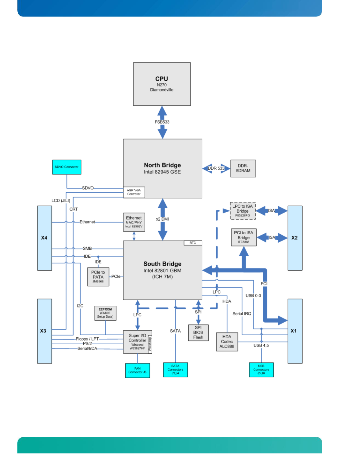
3.4 Block Diagram
Page 13

ETX-DC®/ Specifications
8
3.5 Mechanical Specifications
Dimensions
» 95.0 mm x 114.0 mm (3.75” x 4.5”)
» Height approx. 12 mm (0.4”)
3.6 Electrical Specifications
Supply Voltage
» VCC: 5V DC +/- 5%
» 5V_Stb: 5V DC +/- 5% but always equal or lower VCC
Note: It is recommended to follow the ATX specification for voltage rise times which claims: "The output voltage
shall rise from ≤ 10% of nominal to within the regulation ranges … within 0.1ms to 20ms".
Supply Voltage Ripple
» Maximum 100 mV peak to peak 0 – 20 MHz
Supply Current 5 V_SB
» Typical 50 mA, peak up to 350 mA (S3)
Power Consumption
Detailed Power Consumption measurements in all states and benchmarks for CPU, Graphics and Memory performance
are available in Application Note KEMAP054 at EMD Customer Section
Page 14

ETX-DC®/ Specifications
9
3.7 Environmental Specifications
Temperature
Operating: (with Kontron Embedded Modules GmbH heat-spreader plate assembly):
» Ambient temperature: 0 to +60 °C
» Maximum heatspreader-plate temperature: 0 to +60 °C (*)
» Non-operating: -30 to +85 °C
Note: *The maximum operating temperature with the heatspreader plate is the maximum measurable temperature
on any spot on the heatspreader’s surface. You must maintain the temperature according to the above
specification.
Operating (without Kontron Embedded Modules GmbH heat-spreader plate assembly):
» Maximum operating temperature: 0 to +60 °C (**)
» Non operating: -30 to +85 °C
Note: **The maximum operating temperature is the maximum measurable temperature on any spot on a module’s
surface. You must maintain the temperature according to the above specification.
Humidity
» Operating: 10% to 90% (non condensing)
» Non operating: 5% to 95% (non condensing)
Page 15

ETX-DC®/ Specifications
10
3.8 MTBF
The following MTBF (Mean Time Between Failure) values were calculated using a combination of manufacturer’s test
data, if the data was available, and a Bellcore calculation for the remaining parts.
The Bellcore calculation used is “Method 1 Case 1”. In that particular method the components are assumed to be
operating at a 50 % stress level in a 40° C ambient environment and the system is assumed to have not been burned
in. Manufacturer’s data has been used wherever possible. The manufacturer’s data, when used, is specified at 50° C,
so in that sense the following results are slightly conservative. The MTBF values shown below are for a 40° C in an
office or telecommunications environment. Higher temperatures and other environmental stresses (extreme altitude,
vibration, salt water exposure, etc.) lower MTBF values.
System MTBF (hours): 176102 @ 40°C
Notes: Fans usually shipped with Kontron Embedded Modules GmbH products have 50,000-hour typical operating
life. The above estimates assume no fan, but a passive heat sinking arrangement Estimated RTC battery life
(as opposed to battery failures) is not accounted for in the above figures and need to be considered for
separately. Battery life depends on both temperature and operating conditions. When the Kontron unit has
external power; the only battery drain is from leakage paths.
Page 16
ETX-DC®/ ETX® Connectors
11
IDE Ports
Ethernet
Power Good/Reset Input
ATX PS Control
Speaker
Battery
I2C-Bus
SM-Bus
ISA Bus
VGA
LVDS (JILI)
Serial Ports
PS/2 Keyboard/Mouse
IRDA
Parallel Port
Floppy
PCI Bus
USB
Audio
Serial IRQ
3.3 V for external use
(max. 500 mA)
side view
(connectors only)
top view
(connectors only)
X1
X2
X4
X3
Term
Description
IO-3,3
Bi-directional 3,3 V IO-Signal
IO-5
Bi-directional 5 V IO-Signal
I-3,3
3,3 V Input
I-5
5 V Input
O-3,3
3,3 V Output
O-5
5 V Output
PU
Pull-Up Resistor
PD
Pull-Down Resistor
PWR
Power Connection
Nc
Not Connected / Reserved
4 ETX® Connectors
The pinouts for ETX® Interface Connectors X1, X2, X3, and X4 are documented for convenient reference. Please see
the ETX® Specification and ETX® Design Guide for detailed, design-level information.
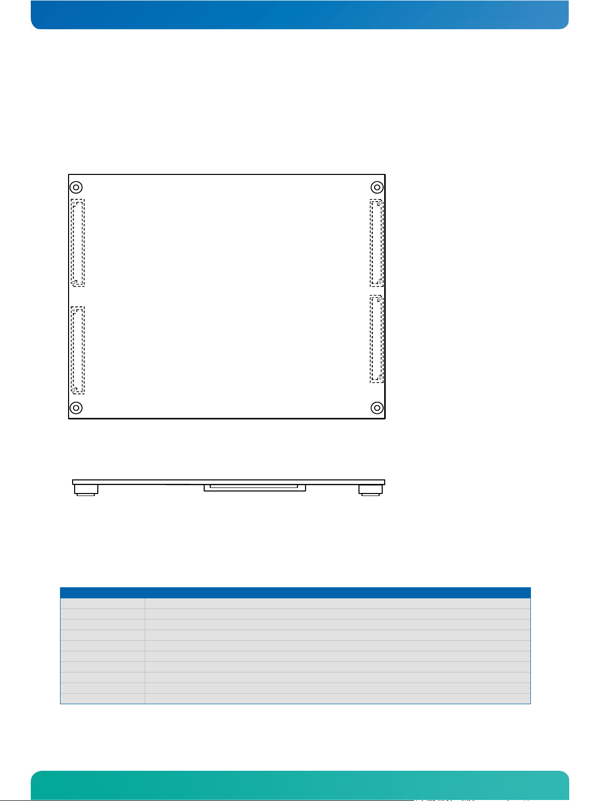
4.1 Connector Locations
4.2 General Signal Description
Page 17
ETX-DC®/ ETX® Connectors
12
Pin
Signal
Pin
Signal
Pin
Signal
Pin
Signal
1
GND 2 GND 51
VCC *
52
VCC *
3
PCICLK3
4
PCICLK4
53
PAR
54
SERR#
5
GND 6 GND 55
GPERR#
56
RESERVED
7
PCICLK1
8
PCICLK2
57
PME#
58
USB2#
9
REQ3#
10
GNT3#
59
LOCK#
60
DEVSEL#
11
GNT2#
12
3V 61
TRDY#
62
USB3#
13
REQ2#
14
GNT1#
63
IRDY#
64
STOP#
15
REQ1#
16
3V 65
FRAME#
66
USB2
17
GNT0#
18
RESERVED
67
GND
68
GND
19
VCC *
20
VCC *
69
AD16
70
CBE2#
21
SERIRQ
22
REQ0#
71
AD17
72
USB3
23
AD0
24
3V 73
AD19
74
AD18
25
AD1
26
AD2 75
AD20
76
USB0#
27
AD4
28
AD3 77
AD22
78
AD21
29
AD6
30
AD5 79
AD23
80
USB1#
31
CBE0#
32
AD7 81
AD24
82
CBE3#
33
AD8
34
AD9 83
VCC *
84
VCC *
35
GND
36
GND 85
AD25
86
AD26
37
AD10
38
AUXAL
87
AD28
88
USB0
39
AD11
40
MIC 89
AD27
90
AD29
41
AD12
42
AUXAR
91
AD30
92
USB1
43
AD13
44
ASVCC
93
PCIRST#
94
AD31
45
AD14
46
SNDL
95
INTC#
96
INTD#
47
AD15
48
ASGND
97
INTA#
98
INTB#
49
CBE1#
50
SNDR
99
GND
100
GND
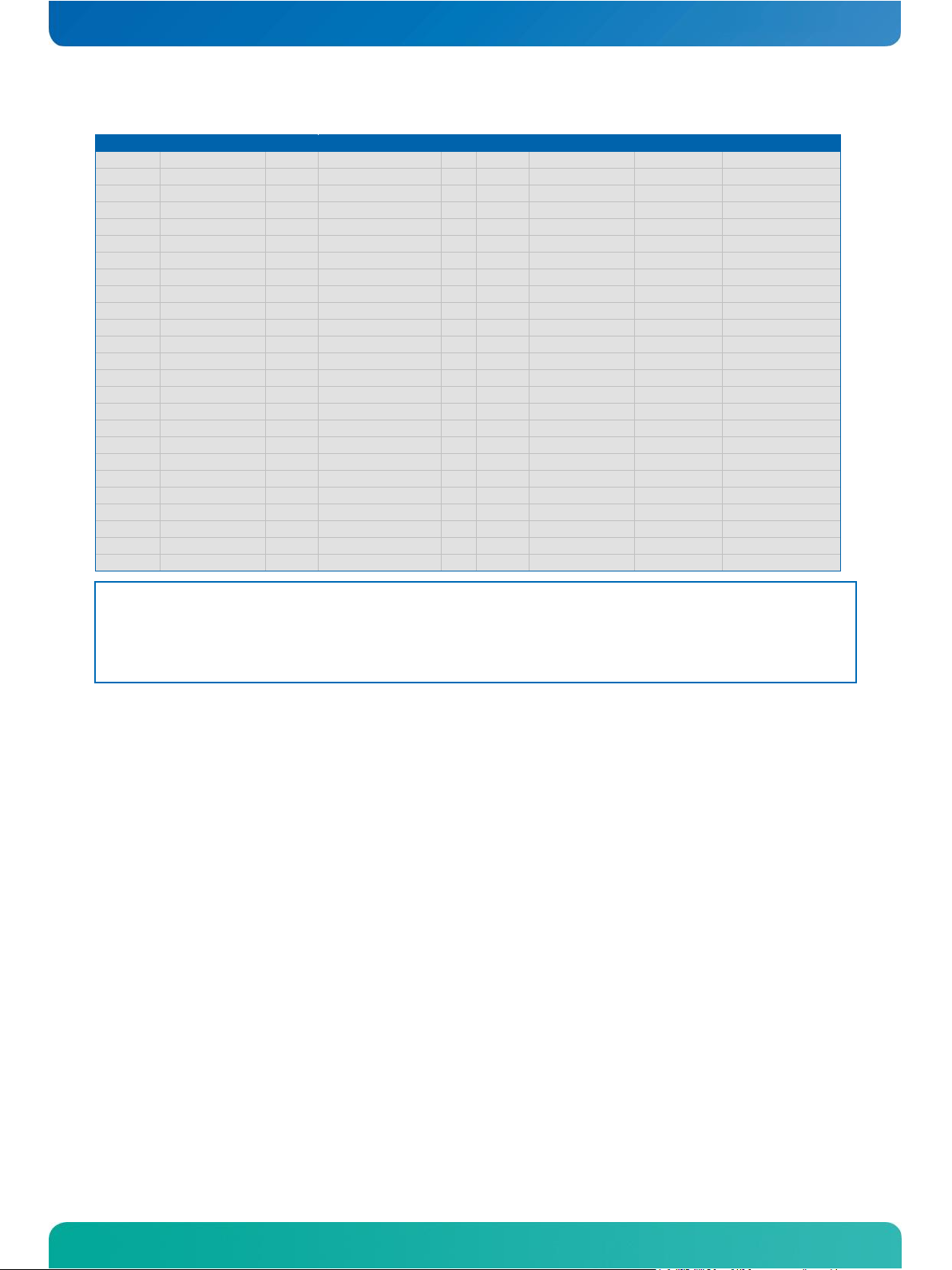
4.3 Connector X1 (PCI bus, USB, Audio)
Notes: * To protect external power lines of peripheral devices, make sure that:
- the wires have the right diameter to withstand the maximum available current
- the enclosure of the peripheral device fulfils the fire-protection requirements of IEC/EN60950
Page 18

ETX-DC®/ ETX® Connectors
13
Pin
Signal
Description
Type
Termination
Comment
1
GND
Ground
PWR - -
2
GND
Ground
PWR - -
3
PCICLK3
PCI Clock Slot 3
O-3,3
-
-
4
PCICLK4
PCI Clock Slot 4
O-3,3
-
-
5
GND
Ground
PWR - -
6
GND
Ground
PWR - -
7
PCICLK1
PCI Clock Slot 1
O-3,3
-
-
8
PCICLK2
PCI Clock Slot 2
O-3,3
-
-
9
REQ3#
PCI Bus Request 3
I-3,3
PU 8k2 3.3V
8k2 Ohm Resistors
10
GNT3#
PCI Bus Grant 3
O-3,3
-
-
11
GNT2#
PCI Bus Grant 2
O-3,3
-
-
12
3V
Power +3,3V
PWR - -
13
REQ2#
PCI Bus Request 2
I-3,3
PU 8k2 3.3V
8k2 Ohm Resistors
14
GNT1#
PCI Bus Grant 1
O-3,3
-
-
15
REQ1#
PCI Bus Request 1
I-3,3
PU 8k2 3.3V
8k2 Ohm Resistors
16
3V
Power +3,3V
PWR - -
17
GNT0#
PCI Bus Grant 0
O-3,3
-
-
18
nc - nc - Reserved
19
VCC
Power +5V
PWR - -
20
VCC
Power +5V
PWR - -
21
SERIRQ
Serial Interrupt Reqest
IO-3,3
PU 8k2
12mA Source sink
22
REQ0#
PCI Bus Request 0
I-3,3
PU 8k2 3.3V
8k2 Ohm Resistors
23
AD0
PCI Adress & Data Bus line
IO-3,3
-
24
3V
Power +3,3V
PWR - -
25
AD1
PCI Adress & Data Bus line
IO-3,3
-
-
26
AD2
PCI Adress & Data Bus line
IO-3,3
-
-
27
AD4
PCI Adress & Data Bus line
IO-3,3
-
-
28
AD3
PCI Adress & Data Bus line
IO-3,3
-
-
29
AD6
PCI Adress & Data Bus line
IO-3,3
-
-
30
AD5
PCI Adress & Data Bus line
IO-3,3
-
-
31
CBE0#
PCI Bus Command and Byte enables 0
IO-3,3
-
-
32
AD7
PCI Adress & Data Bus line
IO-3,3
-
-
33
AD8
PCI Adress & Data Bus line
IO-3,3
-
-
34
AD9
PCI Adress & Data Bus line
IO-3,3
-
-
35
GND
Ground
PWR - -
36
GND
Ground
PWR - -
37
AD10
PCI Adress & Data Bus line
IO-3,3
-
-
38
AUXAL
Auxiliary Line Input Left
I
PD 4k7 ASGND
1:2 bleeder
39
AD11
PCI Adress & Data Bus line
IO-3,3
-
-
40
MIC
Microphone Input
I - -
41
AD12
PCI Adress & Data Bus line
IO-3,3
-
-
42
AUXAR
Auxiliary Line Input Right
I
PD 4k7 ASGND
1:2 bleeder
43
AD13
PCI Adress & Data Bus line
IO-3,3
-
-
44
ASVCC
Analog Supply of Sound Controller
O-5 - -
45
AD14
PCI Adress & Data Bus line
IO-3,3
-
-
46
SNDL
Audio Out Left
O - -
47
AD15
PCI Adress & Data Bus line
IO-3,3
-
-
48
ASGND
Analog Ground of Sound Controller
P - -
49
CBE1#
PCI Bus Command and Byte enables 1
IO-3,3
-
-
50
SNDR
Audio Out Right
O - -
4.3.1 Connector X1 Signal Levels
Pin 1-50 [Power | PCI |USB | AUDIO]
Note: The termination resistors in this table are already mounted on the ETX®board. Please refer to the design
guide for information about additional termination resistors.
Page 19

ETX-DC®/ ETX® Connectors
14
Pin
Signal
Description
Type
Termination
Comment
51
VCC
Power +5V
PWR - -
52
VCC
Power +5V
PWR - -
53
PAR
PCI Bus Parity
IO-3,3
-
-
54
SERR#
PCI Bus System Error
IO-3,3
PU 8k2 3,3V
-
55
GPERR#
PCI Bus Grant Error
IO-3,3
PU 8k2 3,3V
-
56
nc - nc - Reserved
57
PME#
PCI Power Management Event
IO-3,3
-
int. PU 10k 3,3V
58
USB2#
USB Data- , Port2
IO-3,3
-
int. PD 15k in ICH7
59
LOCK#
PCI Bus Lock
IO-3,3
PU 8k2 3,3V
-
60
DEVSEL#
PCI Bus Device Select
IO-3,3
PU 8k2 3,3V
-
61
TRDY#
PCI Bus Target Ready
IO-3,3
PU 8k2 3,3V
-
62
USB3#
USB Data- , Port3
IO-3,3
-
int. PD 15k in ICH7
63
IRDY#
PCI Bus Initiator Ready
IO-3,3
PU 8k2 3,3V
-
64
STOP#
PCI Bus Stop
IO-3,3
PU 8k2 3,3V
-
65
FRAME#
PCI Bus Cycle Frame
IO-3,3
PU 8k2 3,3V
-
66
USB2
USB Data+ , Port2
IO-3,3
-
int. PD 15k in ICH7
67
GND
Ground
PWR - -
68
GND
Ground
PWR - -
69
AD16
PCI Adress & Data Bus line
IO-3,3
-
-
70
CBE2#
PCI Bus Command and Byte enables 2
IO-3,3
-
-
71
AD17
PCI Adress & Data Bus line
IO-3,3
-
-
72
USB3
USB Data+ , Port3
IO-3,3
-
int. PD 15k in ICH7
73
AD19
PCI Adress & Data Bus line
IO-3,3
-
-
74
AD18
PCI Adress & Data Bus line
IO-3,3
-
-
75
AD20
PCI Adress & Data Bus line
IO-3,3
-
-
76
USB0#
USB Data- , Port0
IO-3,3
-
int. PD 15k in ICH7
77
AD22
PCI Adress & Data Bus line
IO-3,3
-
-
78
AD21
PCI Adress & Data Bus line
IO-3,3
-
-
79
AD23
PCI Adress & Data Bus line
IO-3,3
-
-
80
USB1#
USB Data- , Port1
IO-3,3
-
int. PD 15k in ICH7
81
AD24
PCI Adress & Data Bus line
IO-3,3
-
-
82
CBE3#
PCI Command and Byte enables 3
IO-3,3
-
-
83
VCC
Power +5V
PWR - -
84
VCC
Power +5V
PWR - -
85
AD25
PCI Adress & Data Bus line
IO-3,3
-
-
86
AD26
PCI Adress & Data Bus line
IO-3,3
-
-
87
AD28
PCI Adress & Data Bus line
IO-3,3
-
-
88
USB0
USB Data+ , Port0
IO-3,3
-
int. PD 15k in ICH7
89
AD27
PCI Adress & Data Bus line
IO-3,3
-
-
90
AD29
PCI Adress & Data Bus line
IO-3,3
-
-
91
AD30
PCI Adress & Data Bus line
IO-3,3
-
-
92
USB1
USB Data+ , Port1
IO-3,3
-
int. PD 15k in ICH7
93
PCIRST#
PCI Bus Reset
O-3,3
-
PD 100k
94
AD31
PCI Adress & Data Bus line
IO-3,3
-
-
95
INTC#
PCI BUS Interrupt Request C
I-3,3
PU 8k2 3,3V
-
96
INTD#
PCI BUS Interrupt Request D
I-3,3
PU 8k2 3,3V
-
97
INTA#
PCI BUS Interrupt Request A
I-3,3
PU 8k2 3,3V
-
98
INTB#
PCI BUS Interrupt Request B
I-3,3
PU 8k2 3,3V
-
99
GND
Ground
PWR - -
100
GND
Ground
PWR - -
Pin 51–100: [Power | PCI |USB | AUDIO]
Note: The termination resistors in this table are already mounted on the ETX® board. Please refer to the design
guide for information about additional termination resistors.
Page 20

ETX-DC®/ ETX® Connectors
15
4.3.2 Connector X1 Signal Description
PCI Bus
The implementation of this subsystem complies with the ETX® Specification. Implementation information is provided
in the ETX® Design Guide. Refer to the documentation for additional information. The PCI bus with its signals:
AD[31:0], C/BE[3:0]#, DEVSEL#, FRAME#, IRDY#, PAR, GPERR#, REQ[3:0]#, SERR#, STOP#, TRDY#, INT[D:A]# is 5V
tolerant.
USB
Three USB host controllers (two 1.1 UHCI and one EHCI high-speed 2.0 controller) are on the Intel® 82801GB south
bridge device. The USB controllers comply with both versions 1.1 and 2.0 of the USB standard and are backward
compatible. The three controllers implement a root hub, which have two USB ports each.
Configuration
The USB controllers are PCI bus devices. The BIOS allocates required system resources during configuration of the PCI
bus.
Audio
The ETX®-DC PCI audio controller is integrated in the Intel® 82801GB southbridge. The audio codec is compatible
with AC97.
Configuration
The audio controller is a PCI bus device. The BIOS allocates required system resources during configuration of the PCI
device.
Serial IRQ
The serial IRQ pin offers a standardized interface to link interrupt request lines to a single wire.
Configuration
The serial IRQ machine is in “Continuous Mode” per default and can be changed in the BIOS setup, the frame size is 21
frames and the start frame pulse width is 4 clocks.
Page 21
ETX-DC®/ ETX® Connectors
16
Pin
Signal
Pin
Signal
Pin
Signal
Pin
Signal
1
GND 2 GND 51
VCC *
52
VCC *
3
SD14
4
SD15
53
SA6
54
IRQ5 5 SD13
6
MASTER#
55
SA7
56
IRQ6
7
SD12
8
DREQ7
57
SA8
58
IRQ7
9
SD11
10
DACK7#
59
SA9
60
SYSCLK
11
SD10
12
DREQ6
61
SA10
62
REFSH#
13
SD9
14
DACK6#
63
SA11
64
DREQ1
15
SD8
16
DREQ5
65
SA12
66
DACK1#
17
MEMW#
18
DACK5#
67
GND
68
GND
19
MEMR#
20
DREQ0
69
SA13
70
DREQ3
21
LA17
22
DACK0#
71
SA14
72
DACK3#
23
LA18
24
IRQ14
73
SA15
74
IOR#
25
LA19
26
IRQ15
75
SA16
76
IOW#
27
LA20
28
IRQ12
77
SA18
78
SA17
29
LA21
30
IRQ11
79
SA19
80
SMEMR#
31
LA22
32
IRQ10
81
IOCHRDY
82
AEN
33
LA23
34
IO16#
83
VCC *
84
VCC *
35
GND
36
GND 85
SD0
86
SMEMW#
37
SBHE#
38
M16#
87
SD2
88
SD1
39
SA0
40
OSC 89
SD3
90
NOWS#
41
SA1
42
BALE 91
DREQ2
92
SD4
43
SA2
44
TC 93
SD5
94
IRQ9**
45
SA3
46
DACK2#
95
SD6
96
SD7
47
SA4
48
IRQ3 97
IOCHK#
98
RSTDRV
49
SA5
50
IRQ4 99
GND
100
GND
3.3V Power Supply for External Components
The ETX®-DC offers the ability to connect external 3.3V devices to the onboard-generated supply voltage. Pin 12 and
Pin 16 of Connector X1 are used to connect to the +3.3V ±5% power supply. The maximum external load is 500mA.
Contact Kontron Embedded Systems Technical Support for help with this feature.
Warning: Do not connect 3.3 V pins to external 3.3 V supply.
For additional information, refer to the ETX® Design Guide, I2C application notes, and JIDA specifications, all of
which are available on the Kontron Embedded Systems Web site.
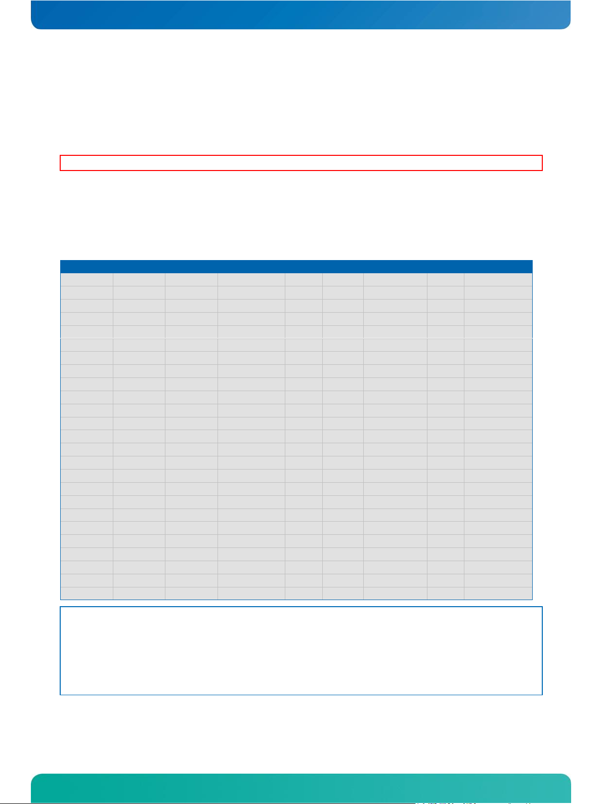
4.4 Connector X2 (ISA Bus)
Notes: *To protect external power lines of peripheral devices, make sure that:
- The wires have the right diameter to withstand the maximum available current.
- The enclosure of the peripheral device fulfils the fire-protection requirements of IEC/EN60950
** IRQ9 is used for SCI in ACPI mode. Do not use for legacy ISA devices.
Page 22
ETX-DC®/ ETX® Connectors
17
Pin
Signal
Description
Type
Termination
Comment
1
GND
Ground
PWR - -
2
GND
Ground
PWR - -
3
SD14
ISA Data Bus
IO-5
PU 8k2 5V
-
4
SD15
ISA Data Bus
IO-5
PU 8k2 5V
-
5
SD13
ISA Data Bus
IO-5
PU 8k2 5V
-
6
MASTER#
ISA 16-Bit Master
I-5
PU 330R 5V
-
7
SD12
ISA Data Bus
IO-5
PU 8k2 5V
-
8
DREQ7
ISA DMA Request 7
I-5
PU 8k2 5V
-
9
SD11
ISA Data Bus
IO-5
PU 8k2 5V
-
10
DACK7#
ISA DMA Acknowledge 7
IO-5 - 24mA source cap.
11
SD10
ISA Data Bus
IO-5
PU 8k2 5V
-
12
DREQ6
ISA DMA Request 6
I-5
PU 8k2 5V
-
13
SD9
ISA Data Bus
IO-5
PU 8k2 5V
-
14
DACK6#
ISA DMA Acknowledge 6
IO-5 - 24mA source cap.
15
SD8
ISA Data Bus
IO-5
PU 8k2 5V
-
16
DREQ5
ISA DMA Request 5
I-5
PU 8k2 5V
-
17
MEMW#
ISA Memory Write
IO-5
PU 8k2 5V
-
18
DACK5#
ISA DMA Acknowledge 5
IO-5 - 24mA source cap.
19
MEMR#
ISA Memory Read
IO-5
PU 8k2 5V
-
20
DREQ0
ISA DMA Request 0
I-5
PU 8k2 5V
-
21
LA17
ISA Adress Bus (SA17)
O-5 - -
22
DACK0#
ISA DMA Acknowledge 0
IO-5 - 24mA source cap.
23
LA18
ISA Adress Bus (SA18)
O-5 - -
24
IRQ14
ISA Interrupt Request 14 / ROM Chip Select
IO-5
PU 8k2 5V
-
25
LA19
ISA Adress Bus (SA19)
O-5 - -
26
IRQ15
ISA Interrupt Request 15
I-5
PU 8k2 5V
-
27
LA20
ISA Latchable Adress Bus
O-5 - -
28
IRQ12
ISA Interrupt Request 12
I-5
PU 8k2 5V
-
29
LA21
ISA Latchable Adress Bus
O-5 - -
30
IRQ11
ISA Interrupt Request 11
I-5
PU 8k2 5V
-
31
LA22
ISA Latchable Adress Bus
O-5 - -
32
IRQ10
ISA Interrupt Request 10
I-5
PU 8k2 5V
-
33
LA23
ISA Latchable Adress Bus
O-5 - -
34
IO16#
ISA 16-Bit I/O Access
I-5
PU 330R 5V
-
35
GND
Ground
PWR - -
36
GND
Ground
PWR - -
37
SBHE#
ISA System Byte High Enable
IO-5 - PU 8k2
38
M16#
ISA 16-Bit Memory Access
IO-5
PU 330R 5V
-
39
SA0
ISA Adress Bus
O-5
PU 8k2 5V
-
40
OSC
ISA Oscillator (CLK_ISA14#)
O-3,3
-
-
41
SA1
ISA Adress Bus
O-5
PU 8k2 5V
-
42
BALE
ISA Buffer Adress Latch Enable
IO-5 - PD 4k7 (Strap)
43
SA2
ISA Adress Bus
O-5
PU 8k2 5V
-
44
TC
ISA Terminal Count
IO-5 - PD 4k7 (Strap)
45
SA3
ISA Adress Bus
O-5
PU 8k2 5V
-
46
DACK2#
ISA DMA Acknowledge 2
IO-5 - -
47
SA4
ISA Adress Bus
O-5
PU 8k2 5V
-
48
IRQ3
ISA Interrupt Request 3
I-5
PU 8k2 5V
-
49
SA5
ISA Adress Bus
O-5
PU 8k2 5V
-
50
IRQ4
ISA Interrupt Request 4
I-5
PU 8k2 5V
-
4.4.1 Connector X2 Signal Levels
Pin 1–50: [Power | ISA]
Note: The termination resistors in this table are already mounted on the ETX® board. Please refer to the design
guide for information about additional termination resistors.
Page 23

ETX-DC®/ ETX® Connectors
18
Pin
Signal
Description
Type
Termination
Comment
51
VCC
Power +5V
PWR - -
52
VCC
Power +5V
PWR - -
53
SA6
ISA Adress Bus
O-3,3
PU 8k2 5V
-
54
IRQ5
ISA Interrupt Request 5
I-3,3
PU 8k2 5V
-
55
SA7
ISA Adress Bus
O-3,3
PU 8k2 5V
-
56
IRQ6
ISA Interrupt Request 6
I-3,3
PU 8k2 5V
-
57
SA8
ISA Adress Bus
O-3,3
PU 8k2 5V
-
58
IRQ7
ISA Interrupt Request 7
I-3,3
PU 8k2 5V
-
59
SA9
ISA Adress Bus
O-3,3
PU 8k2 5V
-
60
SYSCLK
ISA Bus Clock (CLK_SYS_ISA)
O-3,3
-
-
61
SA10
ISA Adress Bus
O-3,3
PU 8k2 5V
-
62
REFSH#
ISA System Refresh Control
IO-3,3
PU 1k 5V
-
63
SA11
ISA Adress Bus
O-3,3
PU 8k2 5V
-
64
DREQ1
ISA DMA Request 1
I-3,3
PU 8k2 5V
-
65
SA12
ISA Adress Bus
O-3,3
PU 8k2 5V
-
66
DACK1#
ISA DMA Acknowledge 1
IO-3,3
-
-
67
GND
Ground
PWR - -
68
GND
Ground
PWR - -
69
SA13
ISA Adress Bus
O-3,3
PU 8k2 5V
-
70
DREQ3
ISA DMA Request 3
I-3,3
PU 8k2 5V
-
71
SA14
ISA Adress Bus
O-3,3
PU 8k2 5V
-
72
DACK3#
ISA DMA Acknowledge 3
IO-3,3
-
-
73
SA15
ISA Adress Bus
O-3,3
PU 8k2 5V
-
74
IOR#
ISA I/O Read
IO-3,3
PU 8k2 5V
-
75
SA16
ISA Adress Bus
O-3,3
PU 8k2 5V
-
76
IOW#
ISA I/O Write
IO-3,3
PU 8k2 5V
-
77
SA18
ISA Adress Bus
O-3,3
PU 8k2 5V
-
78
SA17
ISA Adress Bus
O-3,3
PU 8k2 5V
-
79
SA19
ISA Adress Bus
O-3,3
PU 8k2 5V
-
80
SMEMR#
ISA System Memory Read
IO-3,3
PU 8k2 5V
-
81
IOCHRDY
ISA I/O Channel Ready
IO-3,3
PU 1k 5V
-
82
AEN
ISA Adress Enable
IO-3,3
-
-
83
VCC
Power +5V
PWR - -
84
VCC
Power +5V
PWR - -
85
SD0
ISA Data Bus
IO-3,3
PU 8k2 5V
-
86
SMEMW#
ISA System Memory Write
IO-3,3
PU 8k2 5V
-
87
SD2
ISA Data Bus
IO-3,3
PU 8k2 5V
-
88
SD1
ISA Data Bus
IO-3,3
PU 8k2 5V
-
89
SD3
ISA Data Bus
IO-3,3
PU 8k2 5V
-
90
NOWS#
ISA No Wait Staits
I-3,3
PU 330R 5V
-
91
DREQ2
ISA DMA Request 2
I-3,3
PU 8k2 5V
-
92
SD4
ISA Data Bus
IO-3,3
PU 8k2 5V
-
93
SD5
ISA Data Bus
IO-3,3
PU 8k2 5V
-
94
IRQ9
ISA Interrupt Request 9
I-3,3
PU 8k2 5V
-
95
SD6
ISA Data Bus
IO-3,3
PU 8k2 5V
-
96
SD7
ISA Data Bus
IO-3,3
PU 8k2 5V
-
97
IOCHK#
ISA I/O Channel Check
I-3,3
PU 8k2 5V
-
98
RSTDRV
ISA Reset
O-3,3
-
-
99
GND
Ground
PWR - -
100
GND
Ground
PWR - -
Pin 51-100: [Power | ISA]
Note: The termination resistors in this table are already mounted on the ETX® board. Please refer to the design
guide for information about additional termination resistors.
Page 24

ETX-DC®/ ETX® Connectors
19
4.4.2 Connector X2 Signal Description
ISA Bus Slot
The implementation of this subsystem complies with the ETX® Specification. Implementation information is provided
in the ETX® Design Guide. Refer to the documentation for additional information.
Restrictions:
DMA Transfer: According to the used PCI 2 ISA solution DMA Transfer is not possible.
Page 25
ETX-DC®/ ETX® Connectors
20
LVDS Interface Pinout (JILI)
Pin
Signal
Pin
Signal
1
GND 2 GND
3 R 4 B 5
HSY 6 G
7
VSY 8 DDCK
9
DETECT#**
10
DDDA
11
LCDDO16
12
LCDDO18
13
LCDDO17
14
LCDDO19
15
GND
16
GND
17
LCDDO13
18
LCDDO15
19
LCDDO12
20
LCDDO14
21
GND
22
GND
23
LCDDO8
24
LCDDO11
25
LCDDO9
26
LCDDO10
27
GND
28
GND
29
LCDDO4
30
LCDDO7
31
LCDDO5
32
LCDDO6
33
GND
34
GND
35
LCDDO1
36
LCDDO3
37
LCDDO0
38
LCDDO2
39
VCC *
40
VCC *
41
JILI_DAT
42
LTGIO0**
43
JILI_CLK
44
BLON#
45
BIASON**
46
DIGON
47
COMP**
48
Y**
49
SYNC**
50
C**
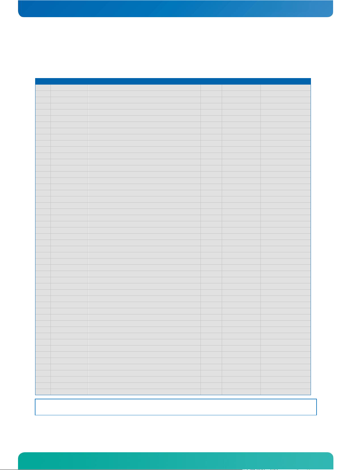
4.5 Connector X3 (VGA, LCD, Video, COM1 and COM2, LPT/Floppy, Mouse,
Keyboard)
4.5.1 Alternative pinning
Flat-Panel Interfaces
ETX®-DC modules can implement an LVDS flat-panel interface called JUMPtec Intelligent LVDS Interface (JILI). These
modules do not implement a parallel digital flat-panel interface called JUMPtec Intelligent Digital Interface (JIDI).
Notes: *To protect external power lines of peripheral devices, make sure that:
- the wires have the right diameter to withstand the maximum available current
- the enclosure of the peripheral device fulfils the fire-protection requirements of IEC/EN60950.
**This signal is not supported on the ETX®-DC.
Page 26

ETX-DC®/ ETX® Connectors
21
Parallel Port Mode Pinout
Floppy Support Mode Pinout
Pin
Signal
Pin
Signal
Pin
Signal
Pin
Signal
51
LPT/FLPY#
52
RESERVED
51
LPT/FLPY#
52
RESERVED
53
VCC *
54
GND 53
VCC *
54
GND
55
STB#
56
AFD# 55
RESERVED
56
DENSEL
57
RESERVED
58
PD7 57
RESERVED
58
RESERVED
59
IRRX
60
ERR# 59
IRRX
60
HDSEL#
61
IRTX
62
PD6 61
IRTX
62
RESERVED
63
RXD2
64
INIT#
63
RXD2
64
DIR#
65
GND
66
GND 65
GND
66
GND
67
RTS2#
68
PD5 67
RTS2#
68
RESERVED
69
DTR2#
70
SLIN#
69
DTR2#
70
STEP#
71
DCD2#
72
PD4 71
DCD2#
72
DSKCHG#
73
DSR2#
74
PD3 73
DSR2#
74
RDATA#
75
CTS2#
76
PD2 75
CTS2#
76
WP#
77
TXD2
78
PD1 77
TXD2
78
TRK0#
79
RI2#
80
PD0 79
RI2#
80
INDEX#
81
VCC *
82
VCC* 81
VCC *
82
VCC *
83
RXD1
84
ACK# 83
RXD1
84
DRV
85
RTS1#
86
BUSY
85
RTS1#
86
MOT
87
DTR1#
88
PE 87
DTR1#
88
WDATA#
89
DCD1#
90
SLCT#
89
DCD1#
90
WGATE#
91
DSR1#
92
MSCLK
91
DSR1#
92
MSCLK
93
CTS1#
94
MSDAT
93
CTS1#
94
MSDAT
95
TXD1
96
KBCLK
95
TXD1
96
KBCLK
97
RI1#
98
KBDAT
97
RI1#
98
KBDAT
99
GND
100
GND 99
GND
100
GND
Parallel Port / Floppy Interfaces
You can configure ETX®-DC’s parallel port interfaces as conventional PC parallel ports or as an interface for a floppydisk drive. You can select the operating mode in the BIOS settings and by a hardware mode-select pin.
If Pin X3-51 (LPT/FLPY#) is grounded at boot time, the floppy support mode is selected. If the pin is left floating or is
held high, parallel-port mode is selected. The mode selection is determined at boot time. It cannot be changed until
the next boot cycle.
Notes: *To protect external power lines of peripheral devices, make sure that:
- the wires have the right diameter to withstand the maximum available current
- the enclosure of the peripheral device fulfils the fire-protection requirements of IEC/EN60950
Page 27

ETX-DC®/ ETX® Connectors
22
Pin
Signal
Description
Type
Termination
Comment
1
GND
Ground
PWR - -
2
GND
Ground
PWR - -
3 R Analog Video Out RGB - Red Channel
O - -
4 B Analog Video Out RGB - Blue Channel
O - -
5
HSY
Horizontal Synchronization Pulse
O-3,3
-
-
6 G Analog Video Out RGB - Green Channel
O - -
7
VSY
Vertical Synchronization Pulse
O-3,3
-
-
8
DDCK
Display Data Channel Clock
IO-5
PU 2k2 5V
-
9
DETECT#
Panel Hot-Plug Detection
IO - ICHGPIO 10
10
DDDA
Display Data Channel Data
IO-5
PU 2k2 5V
-
11
LCDDO16
LVDS Channel Data
O - -
12
LCDDO18
LVDS Channel Data
O Only available on -4
13
LCDDO17
LVDS Channel Data
O - -
14
LCDDO19
LVDS Channel Data
O - Only available on -4
15
GND
Ground
PWR - -
16
GND
Ground
PWR - -
17
LCDDO13
LVDS Channel Data
O - -
18
LCDDO15
LVDS Channel Data
O - -
19
LCDDO12
LVDS Channel Data
O - -
20
LCDDO14
LVDS Channel Data
O - -
21
GND
Ground
PWR - -
22
GND
Ground
PWR - -
23
LCDDO8
LVDS Channel Data
O Only available on -4
24
LCDDO11
LVDS Channel Data
O - -
25
LCDDO9
LVDS Channel Data
O Only available on -4
26
LCDDO10
LVDS Channel Data
O - -
27
GND
Ground
PWR - -
28
GND
Ground
PWR - -
29
LCDDO4
LVDS Channel Data
O - -
30
LCDDO7
LVDS Channel Data
O - -
31
LCDDO5
LVDS Channel Data
O - -
32
LCDDO6
LVDS Channel Data
O - -
33
GND
Ground
PWR - -
34
GND
Ground
PWR - -
35
LCDDO1
LVDS Channel Data
O - -
36
LCDDO3
LVDS Channel Data
O - -
37
LCDDO0
LVDS Channel Data
O - -
38
LCDDO2
LVDS Channel Data
O - -
39
VCC
Power +5V
PWR - -
40
VCC
Power +5V
PWR - -
41
JILI_DAT
JILI I2C Data Signal
IO-3,3
PU 2k2 3,3V
-
42
LTGIO0
PWM Brightness control for LCD
O-3,3
-
-
43
JILI_CLK
JILI I2C Clock Signal
IO-3,3
PU 2k2 3,3V
-
44
BLON#
Display Backlight On
O-3,3
-
-
45
BIASON
Display Contrast
IO - SIO_GP35
46
DIGON
Display Power On
O-3,3
-
-
47
COMP
Composite Video / SCART Blue
O - -
48 Y S-Video Luminance / SCART Red
O - -
49
SYNC - nc - Not supported
50 C S-Video Chrominance / SCART Green
O - -
4.5.2 Connector X3 (Signal Levels)
Pin 1–50: [Power | VGA |LCD| TV]
Note: The termination resistors in this table are already mounted on the ETX® board. Please refer to the design
guide for information about additional termination resistors.
Page 28

ETX-DC®/ ETX® Connectors
23
Pin
Signal
Description
Type
Termination
Comment
51
LPT | FLPY#
LPT / Floppy Interface Configuration Input
I-5
PU 10K 3V
H: LPT, L: Floppy
52
nc - nc - Reserved
53
VCC
Power +5V
PWR - -
54
GND
Ground
PWR - -
55
STB# | nc
LPT Strobe Signal
O-5 - -
56
AFD# | DENSEL
LPT Automatic Feed / Floppy Density Select
O-5 - -
57
nc - nc - Reserved
58
PD7 | nc
LPT Data Bus D7
IO-5 - -
59
IRRX
Infrared Receive
I-5 - -
60
ERR# | HDSEL#
LPT Error / Floppy Head Select
IO-5 - -
61
IRTX
Infrared Transmit
O-5 - -
62
PD6 | nc
LPT Data Bus D6
IO-5 - -
63
RXD2
Data Receive COM2
I-5 - -
64
INIT# | DIR#
LPT Initiate / Floppy Direction
O-5 - -
65
GND
Ground
PWR - -
66
GND
Ground
PWR - -
67
RTS2#
Request to Send COM2
O-5
PU 100k 3,3V
-
68
PD5 | nc
LPT Data Bus D5
IO-5 - -
69
DTR2#
Data Terminal Ready COM2
O-5
PU 100k 3,3V
-
70
SLIN# | STEP#
LPT Select / Floppy Motor Step
O-5 - -
71
DCD2#
Data Carrier Detect COM2
I-5
PU 4k7 5V
-
72
PD4 | DSKCHG#
LPT Data Bus D4 / Floppy Disk Change
IO-5 - -
73
DSR2#
Data Set Ready COM2
I-5
PU 4k7 5V
-
74
PD3 | RDATA#
LPT Data Bus D3 / Floppy Raw Data Read
IO-5 - -
75
CTS2#
Clear to Send COM2
I-5
PU 4k7 5V
-
76
PD2 | WP#
LPT Data Bus D2 / Floppy Write Protect Signal
IO-5 - -
77
TXD2
Data Transmit COM2
O-5 - -
78
PD1 | TRK0#
LPT Data Bus D1 / Floppy Track Signal
IO-5 - -
79
RI2#
Ring Indicator COM2
I-5
PU 4k7 5V
-
80
PD0 | INDEX#
LPT Data Bus D0 / Floppy Index Signal
IO-5 - -
81
VCC
Power +5V
PWR - -
82
VCC
Power +5V
PWR - -
83
RXD1
Data Receive COM1
O-5
PU 100k 3,3V
-
84
ACK# | DRV
LPT Acknowledge / Floppy Drive Select
IO-5 - -
85
RTS1#
Request to Send COM1
O-5
PU 1k 3,3V
Bootstrap
86
BUSY# | MOT
LPT Busy / Floppy Motor Select
IO-5 - -
87
DTR1#
Data Terminal Ready COM1
O-5
PU 1k 3,3V
Bootstrap
88
PE | WDATA#
LPT Paper Empty / Floppy Raw Write Data
IO-5 - -
89
DCD1#
Data Carrier Detect COM1
I-5
PU 100k 3,3V
-
90
SLCT#|WGATE#
LPT Power On / Floppy Write Enable
IO-5 - -
91
DSR1#
Data Set Ready COM1
I-5
PU 100k 3,3V
-
92
MSCLK
Mouse Clock
O-5
PU 4k7 3,3V
-
93
CTS1#
Clear to Send COM1
I-5
PU 100k 3,3V
-
94
MSDAT
Mouse Data
IO-5
PU 4k7 3,3V
-
95
TXD1
Data Transmit COM1
O-5
PU 1k 3,3V
Bootstrap
96
KBCLK
Keyboard Clock
O-5
PU 4k7 3,3V
-
97
RI1#
Ring Indicator COM1
I-5
PU 100k 3,3V
-
98
KBDAT
Keyboard Data
IO-5
PU 4k7 3,3V
-
99
GND
Ground
PWR - -
100
GND
Ground
PWR - -
Pin 51–100: [Power | COM |LPT | Floppy | KB/MS/IR]
Note: The termination resistors in this table are already mounted on the ETX® board. Please refer to the design
guide for information about additional termination resistors.
Page 29

ETX-DC®/ ETX® Connectors
24
4.6 Connector X3 Signal Description
VGA Output
LVDS Flat Panel Interface (JILI)
The user interface for flat panels is the JUMPtec Intelligent LVDS Interface (JILI). The implementation of this
subsystem complies with the ETX® Specification. Implementation information is provided in the ETX® Design Guide.
Refer to the documentation for additional information.
Digital Flat Panel Interface (JIDI)
The ETX®-DC does not support the JUMPtec Intelligent Digital Interface (JIDI).
Serial Ports (1 and 2)
The ETX®-DC supports two serial interfaces (TTL). You can use COM2 for IrDA SIR operation. This feature is
implemented in the super I/O device, which is a Winbond 83627HF.
The implementation of the serial interface complies with the ETX® Specification. Implementation information is
provided in the ETX® Design Guide. Refer to the documentation for additional information.
Configuration:
The serial-communication interface uses I/O and IRQ resources. The resources are allocated by the BIOS during POST
configuration and are set to be compatible with common PC/AT settings. Use the BIOS setup to change some
parameters that relate to the serial-communication interface.
PS/2 Keyboard
The implementation of the keyboard interface complies with the ETX® Specification. Implementation information is
provided in the ETX® Design Guide. Refer to the documentation for additional information.
Configuration:
The keyboard uses I/O and IRQ resources. The BIOS allocates the resources during POST configuration. The resources
are set to be compatible with common PC/AT settings. Use the BIOS setup to change some keyboard-related
parameters.
PS/2 Mouse
The implementation of the mouse interface complies with the ETX® Specification. Implementation information is
provided in the ETX® Design Guide. Refer to the documentation for additional information.
Configuration:
Page 30

ETX-DC®/ ETX® Connectors
25
The mouse uses I/O and IRQ resources. The BIOS allocates the resources during POST configuration. The resources are
set to be compatible with common PC/AT settings. You can change some mouse-related parameters from the BIOS
setup.
IrDA
The ETX®-DC is capable of IrDA SIR operation. This feature is implemented in the Winbond 83627HF. Contact Kontron
Embedded Modules for help with this feature.
Parallel Port
The parallel-communication interface shares signals with the floppy-disk interface. The implementation of this
parallel port complies with the ETX® Specification. Implementation information is provided in the ETX® Design Guide.
Refer to the documentation for additional information.
Configuration:
The parallel-communication interface uses I/O, IRQ, and DMA resources. The resources are allocated by the BIOS
during POST configuration and are set to be compatible with common PC/AT settings. You can change some
parameters of the parallel-communication interface through the BIOS setup.
Floppy
The floppy-disk interface shares signals with the parallel-communication interface. The floppy interface is limited to
one drive (drive_1). A standard floppy cable has two connectors for floppy drives. One connector has a non-twisted
cable leading to it, the other has a twisted cable leading to it. When using the floppy interface you must connect the
floppy drive to the connector (drive_1) that has the non-twisted cable leading to it.
The implementation of this subsystem complies with the ETX® Specification. Implementation information is provided
in the ETX® Design Guide. Refer to the documentation for additional information.
Configuration:
The floppy-disk controller uses I/O, IRQ, and direct memory access (DMA) resources. These resources are allocated by
BIOS during POST configuration and are compatible with common PC/AT settings. You can change some parameters of
the parallel-communication interface through the BIOS setup.
Page 31

ETX-DC®/ ETX® Connectors
26
Pin
Signal
Pin
Signal
Pin
Signal
Pin
Signal
1
GND 2 GND 51
SIDE_IOW#
52
PIDE_IOR#
3
5V_SB
4
PWGIN
53
SIDE_DRQ
54
PIDE_IOW#
5
PS_ON
6
SPEAKER
55
SIDE_D15
56
PIDE_DRQ
7
PWRBTN#
8
BATT 57
SIDE_D0
58
PIDE_D15
9
KBINH#
10
LILED#
59
SIDE_D14
60
PIDE_D0
11
RSMRST#
12
ACTLED#
61
SIDE_D1
62
PIDE_D14
13
ROMKBCS#
14
SPEEDLED#
63
SIDE_D13
64
PIDE_D1
15
EXT_PRG
16
I2CLK
65
GND
66
GND
17
VCC*
18
VCC* 67
SIDE_D2
68
PIDE_D13
19
OVCR#
20
GPCS#
69
SIDE_D12
70
PIDE_D2
21
EXTSMI#
22
I2DAT
71
SIDE_D3
72
PIDE_D12
23
SMBCLK
24
SMBDATA
73
SIDE_D11
74
PIDE_D3
25
SIDE_CS3#
26
RESERVED
75
SIDE_D4
76
PIDE_D11
27
SIDE_CS1#
28
DASP_S
77
SIDE_D10
78
PIDE_D4
29
SIDE_A2
30
PIDE_CS3#
79
SIDE_D5
80
PIDE_D10
31
SIDE_A0
32
PIDE_CS1#
81
VCC
82
VCC
33
GND
34
GND 83
SIDE_D9
84
PIDE_D5
35
PDIAG_S
36
PIDE_A2
85
SIDE_D6
86
PIDE_D9
37
SIDE_A1
38
PIDE_A0
87
SIDE_D8
88
PIDE_D6
39
SIDE_INTRQ
40
PIDE_A1
89
GPE2#
90
CBLID_P#
41
RESERVED
42
RESERVED
91
RXD#
92
PIDE_D8
43
SIDE_AK#
44
PIDE_INTRQ
93
RXD
94
SIDE_D7
45
SIDE_RDY
46
PIDE_AK#
95
TXD#
96
PIDE_D7
47
SIDE_IOR#
48
PIDE_RDY
97
TXD
98
HDRST#
49
VCC*
50
VCC* 99
GND
100
GND
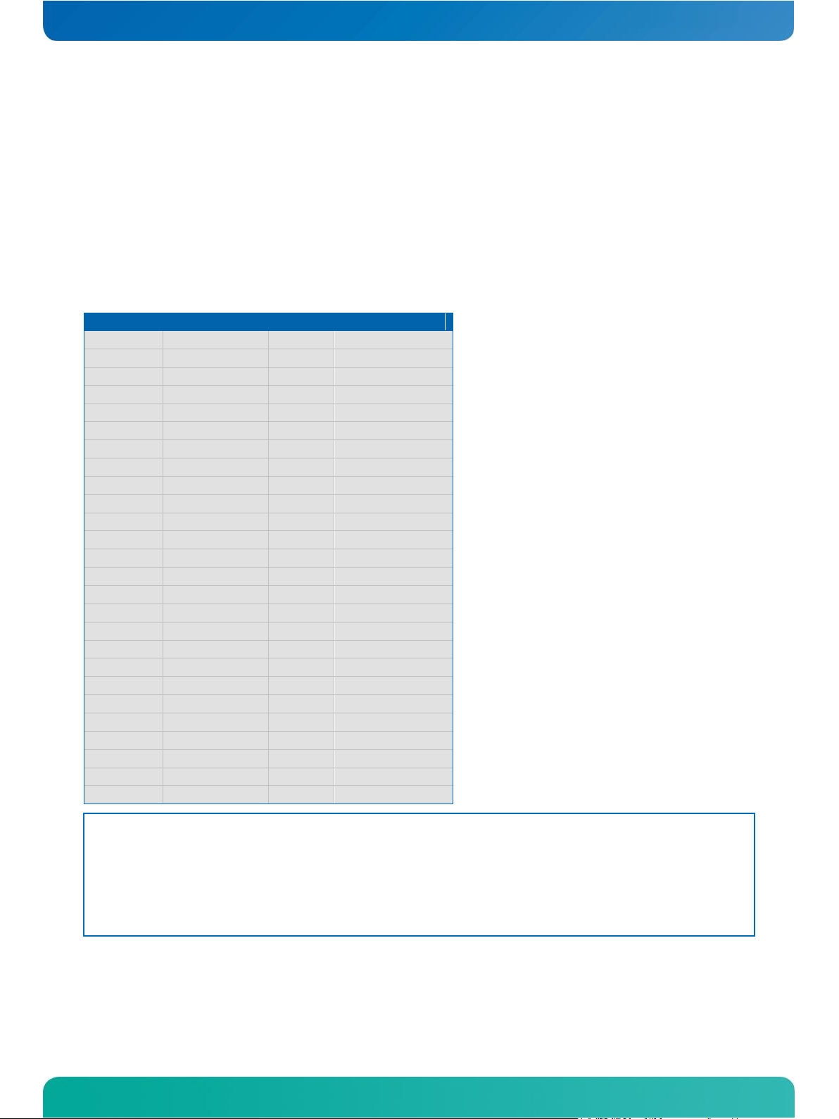
4.7 Connector X4 Subsystems
4.7.1 Connector X4 (IDE 1, IDE 2, Ethernet, Miscellaneous)
Notes: *To protect external power lines of peripheral devices, make sure that:
- the wires have the right diameter to withstand the maximum available current
- the enclosure of the peripheral device fulfils the fire-protection requirements of IEC/EN60950
Page 32

ETX-DC®/ ETX® Connectors
27
Pin
Signal
Description
Type
Termination
Comment
1
GND
Ground
PWR - -
2
GND
Ground
PWR - -
3
5V_SB
Supply of internal suspend Circuit
PWR - 5V_SB ≤ VCC
4
PWGIN
Power Good / Reset Input
I - -
5
PS_ON
Power Supply On
O-5V
-
-
6
SPEAKER
Speaker Output
O-3.3
-
int. PD 20k ( ICH7-M)
7
PWRBTN#
Power Button
I-5V
PU 10k 5V
-
8
BATT
Battery Supply
I - 3V
9
KBINH
Keyboard Inhibit Control Input
I-5 - not used
10
LILED
Ethernet Link LED
O-3,3
-
-
11
RSMRST#
Resume Reset
nc
PU 10k 3,3V
Not supported
12
ACTLED
Ethernet Activity LED
O-3,3
-
-
13
ROMKBCS#
- O -
PATA LED
14
SPEEDLED
Ethernet Speed LED
O-3,3
-
on at 100Mb/s
15
EXT_PRG
-
nc - not supported
16
I2CLK
I2C Bus Clock
O-5
PU 2k2 5V
-
17
VCC
Power +5V
PWR - -
18
VCC
Power +5V
PWR - -
19
OVCR#
Over Current Detect for USB
I-3,3
PU 10k 3,3V
-
20
GPCS#
-
nc - not supported
21
EXTSMI#
System Management Interrupt Input
I-3,3
PU 10k 3,3V
-
22
I2DAT
I2C Bus Data
IO-5
PU 2k2 5V
-
23
SMBCLK
SM Bus Clock
O-3,3
PU 2k2 3,3V
-
24
SMBDATA
SM Bus Data
IO-3,3
PU 2k2 3,3V
-
25
SIDE_CS3#
Secondary IDE Chip Select Channel 1
O-3,3
-
-
26
SMBALERT
SMB Alert
I-3,3
PU 10k 3,3V
-
27
SIDE_CS1#
Secondary IDE Chip Select Channel 0
O-3,3
-
-
28
DASP_S
-
nc - not supported
29
SIDE_A2
Seconary IDE Address Bus
O-3,3
-
-
30
PIDE_CS3#
Primary IDE Chip Select Channel 1
O-3,3
-
-
31
SIDE_A0
Seconary IDE Address Bus
O-3,3
-
-
32
PIDE_CS1#
Primary IDE Chip Select Channel 0
O-3,3
-
-
33
GND
Ground
PWR - -
34
GND
Ground
PWR - -
35
PDIAG_S
Secondary IDE Diagnosis Signal
I-3,3
PD 10k
-
36
PIDE_A2
Primary IDE Address Bus
O-3,3
-
-
37
SIDE_A1
Secondary IDE Address Bus
O-3,3
-
-
38
PIDE_A0
Primary IDE Address Bus
O-3,3
-
-
39
SIDE_INTRQ
Secondary IDE Interrupt Reqeuest
I-3,3
PD 10k
-
40
PIDE_A1
Primary IDE Address Bus
O-3,3
-
-
41
PM_BATLOW#
Battery Low
I-3,3
PU 8k2 3,3V
-
42
GPE1#
General Purpose Power Event 1
I-3,3
PU 10k 3,3V
GPIO15 on ICH7-M
43
SIDE_AK#
Secondary IDE DMA Acknowledge
O-3,3
-
-
44
PIDE_INTRQ
Primary IDE Interrupt Reqeuest
I-3,3
PU 8k2 3,3V
-
45
SIDE_RDY
Secondary IDE Ready
I-3,3
PU 4k7,3V
-
46
PIDE_AK#
Primary IDE DMA Acknowledge
O-3,3
-
-
47
SIDE_IOR#
Secondary IDE IO Read
O-3.3
-
-
48
PIDE_RDY
Primary IDE Ready
I-3,3
PU 4k7,3V
-
49
VCC
Power +5V
PWR - -
50
VCC
Power +5V
PWR - -
4.7.2 Connector X4 (Signal Levels)
Pin 1–50: [Power | IDE |Ethernet | Power control | Misc]
Note: The termination resistors in this table are already mounted on the ETX® board. Please refer to the design
guide for information about additional termination resistors.
Page 33

ETX-DC®/ ETX® Connectors
28
Pin
Signal
Description
Type
Termination
Comment
51
SIDE_IOW#
Secondary IDE IO Write
O-3,3
-
-
52
PIDE_IOR#
Primary IDE IO Read
O-3,3
-
-
53
SIDE_DRQ
Secondary IDE DMA Request
I-3,3
PD 5k6
-
54
PIDE_IOW#
Primary IDE IO Write
O-3,3
-
-
55
SIDE_D15
Secondary IDE Data Bus
IO - -
56
PIDE_DRQ
Primary IDE DMA Request
I-3,3 - -
57
SIDE_D0
Secondary IDE Data Bus
IO - -
58
PIDE_D15
Primary IDE Data Bus
IO - -
59
SIDE_D14
Secondary IDE Data Bus
IO - -
60
PIDE_D0
Primary IDE Data Bus
IO - -
61
SIDE_D1
Secondary IDE Data Bus
IO - -
62
PIDE_D14
Secondary IDE Data Bus
IO - -
63
SIDE_D13
Secondary IDE Data Bus
IO - -
64
PIDE_D1
Primary IDE Data Bus
IO - -
65
GND
Ground
PWR - -
66
GND
Ground
PWR - -
67
SIDE_D2
Secondary IDE Data Bus
IO - -
68
PIDE_D13
Primary IDE Data Bus
IO - -
69
SIDE_D12
Secondary IDE Data Bus
IO - -
70
PIDE_D2
Primary IDE Data Bus
IO - -
71
SIDE_D3
Secondary IDE Data Bus
IO - -
72
PIDE_D12
Primary IDE Data Bus
IO - -
73
SIDE_D11
Secondary IDE Data Bus
IO - -
74
PIDE_D3
Primary IDE Data Bus
IO - -
75
SIDE_D4
Secondary IDE Data Bus
IO - -
76
PIDE_D11
Primary IDE Data Bus
IO - -
77
SIDE_D10
Secondary IDE Data Bus
IO - -
78
PIDE_D4
Primary IDE Data Bus
IO - -
79
SIDE_D5
Secondary IDE Data Bus
IO - -
80
PIDE_D10
Primary IDE Data Bus
IO - -
81
VCC
Power +5V
PWR - -
82
VCC
Power +5V
PWR - -
83
SIDE_D9
Secondary IDE Data Bus
IO - -
84
PIDE_D5
Primary IDE Data Bus
IO - -
85
SIDE_D6
Secondary IDE Data Bus
IO - -
86
PIDE_D9
Primary IDE Data Bus
IO - -
87
SIDE_D8
Secondary IDE Data Bus
IO - -
88
PIDE_D6
Primary IDE Data Bus
IO - -
89
GPE2#
General Purpose Power Event 1
I-3,3
PU 10k 3,3V
RI of ICH7M
90
CBLID_P#
80-conductor IDE cable Channel 0
I-3,3
PD 10k
-
91
RXD#
Ethernet Receive Differential Signal ( RXD-)
I - 121R between RXD+/-
92
PIDE_D8
Primary IDE Data Bus
IO - -
93
RXD
Ethernet Receive Differential Signal ( RXD+)
I - 121R between RXD+/-
94
SIDE_D7
Secondary IDE Data Bus
IO - -
95
TXD#
Ethernet Transmit Differential Signal (TXD-)
O - 100R/C10p between
96
PIDE_D7
Primary IDE Data Bus
IO - int. PD 11k5 ICH7-M
97
TXD
Ethernet Transmit Differential Signal (TXD+)
O - 100R/C10p between
98
HDRST#
Hard Drive Reset
O-5 - -
99
GND
Ground
PWR - -
100
GND
Ground
PWR - -
Pin 51–100: [Power | IDE |Ethernet | Misc]
Note: The termination resistors in this table are already mounted on the ETX® board. Please refer to the design
guide for information about additional termination resistors.
Page 34

ETX-DC®/ ETX® Connectors
29
4.7.3 Connector X4 Signal Description
IDE Ports
The IDE host adapter is capable of DMA-100 operation and supports only one single IDE channel which is connected to
the primary channel of the ETX® connector X4. Per default it is set to DMA-33, to achieve the best compatibility to
most baseboard implementations. Implementation information is provided in the ETX® Design Guide. Refer to those
documents for additional information.
Configuration:
The IDE host adapter is a PCI bus device. It is configured by the BIOS during PCI device configuration. You can disable
it in setup. Resources used by the primary IDE host adapter are compatible with the PC/AT.
Ethernet
The Ethernet interface is based on the Intel® 82562 Fast Ethernet PCI controller. This 32-bit PCI controller is a fully
integrated 10/100BASE-TX LAN solution.
The Ethernet interface requires an external transformer. See the ETX® Design Guide for suggestions on transformer
selection.
Configuration:
The Ethernet interface is a PCI device. The BIOS setup automatically configures it during configuration of the PCI
device.
Note: Implementation and limitation information is provided in the ETX® Design Guide from document revision
2.1. Refer to the documentation for additional information.
Power Control
Power Good / Reset Input:
The ETX®-DC provides an external input for a power-good signal or a manual- reset pushbutton. The implementation
of this subsystem complies with the ETX® Specification. Implementation information is provided in the ETX® Design
Guide. Refer to the documentation for additional information.
Power Management
ATX PS Control:
The ETX®-DC can control the main power output of an ATX-style power supply. The implementation of this subsystem
complies with the ETX® Specification. Implementation information is provided in the ETX® Design Guide. Refer to the
documentation for additional information.
Page 35

ETX-DC®/ ETX® Connectors
30
BIOS Setup Selection
Measured I2C Speed
Very High
125 kHz
High
62.5 kHz
Medium
31.25 kHz
Slow
8 kHz
Very Slow
1.25 kHz
Ultra Slow
530 Hz
External SMI Interrupt:
Contact Kontron Embedded Modules GmbH technical support for information on this feature.
Miscellaneous Circuits
Speaker
The implementation of the speaker output complies with the ETX® Specification. Implementation information is
provided in the ETX® Design Guide. Refer to the documentation for additional information.
Battery
The implementation of the battery input complies with the ETX® Specification. Implementation information is
provided in the ETX® Design Guide. Refer to the documentation for additional information.
In compliance with EN60950, there are at least two current-limiting devices (resistor and diode) between the battery
and the consuming component.
I2C Bus
The external I2C provided via GPIOs on ETX® Connector Pin 16 and 22 on X4 offers full MultiMaster and Clock
Stretching support. See the tables below for measured values on ETX®-DC with BIOS MNP1R112.
You can access the I2C Bus via JUMPtec’s Intelligent Device Architecture (JIDA) BIOS functions.
For additional information, refer to the ETX® Design Guide, I2C application notes and JIDA specification which are
available at the Kontron Web site.
SM Bus
System Management (SM) bus signals are connected to the SM bus controller, which is located in the southbridge
(Intel 82801GBM) device. For more information about the SM bus, please see the System Management (SM) Bus
section in the Appendix A: System Resources chapter.
Page 36

ETX-DC®/ ETX® Connectors
31
4.8 SDVO Connector J9
4.8.1 Location of the connector
The feature connector J9 is on the bottom side of the module on the edge.
4.8.2 SDVO Output
The ETX®-DC Serial Digital Video Out port is integrated in the Intel® 945GSE northbridge. It has the following
features:
» Serial Digital Video Out Port (SDVOB only) support
» One 12-bit channel
» The SDVO B port can drive a variety of SDVO devices (TV-Out Encoders, TMDS and LVDS transmitters, etc.)
Page 37

ETX-DC®/ ETX® Connectors
32
4.8.3 Connector and Flat Foil Cable
Connector and flat foil cable information for the SDVO connector (J9) located on the bottom side.
Flat Foil Cable
» YOUNGSHIN MCAB45x150B05
» 45pos,150 mm length, 0.5mm pitch, both ends opposite sides
Connector
» Hirose - FH12-45S-0.5SH
» 0.50mm (.020") Pitch FFC/FPC Connector, Horizontal Right Angle, SMT, 45 Circuits
4.8.4 Software Requirements
SDVO Output during bootup
The BIOS must be set to enable the SDVO output during boot-up. Please enter the BIOS setup tool by pressing the
<del> button during boot-up and go into the menu
Chipset Control -> North Bridge Configuration -> Display Control
Please change the setting Boot Display Device to either "SDVO" or "CRT + SDVO".
SDVO Output during runtime
The regarding driver must enable the interface. This does not need an enabled boot up display set to SDVO.
Page 38

ETX-DC®/ ETX® Connectors
33
Pin
Pin on ETX®-CD
Description
1
GND1
Ground
2
SDVOC_CLKN
nc
3
SDVOC_CLKN
nc
4
GND2
Ground
5
SDVOC_GREENN
nc
6
SDVOC_GREENP
nc
7
GND3
Ground
8
SDVOB_CLKN
Channel B; Clock negative
9
SDVOB_CLKN
Channel B; Clock positive
10
GND4
Ground
11
SDVOB_GREENN
Channel B; Green negative
12
SDVOB_GREENP
Channel B; Green positive
13
GND5
Ground
14
SDVOC_INTN
nc
15
SDVOC_INTP
nc
16
GND6
Ground
17
SDVOB_INTN
Channel B; Interrupt negative
18
SDVOB_INTP
Channel B; Interrupt positive
19
GND7
Ground
20
SDVOC_BLUEN
nc
21
SDVOC_BLUEP
nc
22
GND8
Ground
23
SDVOC_REDN
nc
24
SDVOC_REDP
nc
25
GND9
Ground
26
SDVOB_BLUEN
Channel B; Blue negative
27
SDVOB_BLUEP
Channel B; Blue positive
28
GND10
Ground
29
SDVOB_REDN
Channel B; Red negative
30
SDVOB_REDP
Channel B; Red positive
31
GND11
Ground
32
SDVO_FLDSTALLN
Field Stall negative
33
SDVO_FLDSTALLP
Field Stall positive
34
GND12
Ground
35
SDVO_TVCLKINN
TV Clock Input negative
36
SDVO_TVCLKINP
TV Clock Input positive
37
GND13
Ground
38
SDVO_CTRCLK
I2C based control signal for SDVO devices; clock
39
SDVO_CTRLDATA
I2C based control signal for SDVO devices; data
40
RESET#
Reset signal
41
VCC
5V power
42
VCC
5V power
43
VCC
5V power
44
Reserved
Nc
45
Reserved
Nc
When you have as boot display device SDVO enabled and you have installed a windows operating system then after the
graphic driver installation your SDVO interface is disabled. You can enable it in blind mode by pressing the key
combination <CTRL><ALT><F4>.
4.8.5 Pinout Feature Connector J9
Page 39

ETX-DC®/ Special Features
34
5 Special Features
5.1 Watchdog Timer
The watchdog timer is implemented within the Winbond W83627HG. The WDT can also be controlled by the JIDA BIOS
support. The application software should strobe the WDT to prevent its timeout. Upon timeout, the WDT resets and
restarts the system. This provides a way to recover from program crashes or lockups.
Configuration
You can program the timeout period for the watchdog timer in two ranges:
» 1-second increments from 1 to 255 seconds
» 1-minute increments from 1 to 255 minutes
The watchdog can release a NMI or a reset.
Contact Kontron Embedded Modules technical support for information on programming and operating the WDT.
5.2 SATA Support
The ETX®-DC supports two SATA ports compliant to the ETX® 3.0 specification
5.3 Restrictions
The ETX-DC® has following restrictions compared to some other ETX® products:
5.3.1 ISA Bus
The ETX-DC® is usually equipped with a PCI2ISA bridge which does not support DMA transfers; therefore e.g. the
floppy interface of an external SuperI/O controller is not supported.
Optionally a LPC2ISA bridge can be equipped as a customized version of the product, but then there is only very
limited memory access on ISA bus possible.
5.3.2 ISA VGA
There is no support for ISA graphic cards on ETCX-DC®.
5.3.3 LVDS
The ETX-DC® supports only 18bit LVDS panels, because only 3 LVDS data pairs are supported by the chipset.
Page 40

ETX-DC®/ Design Considerations
35
6 Design Considerations
6.1 Thermal Management
A heat-spreader plate assembly is available from Kontron Embedded Modules GmbH for the ETX®-DC. The heatspreader plate on top of this assembly is NOT a heat sink. It works as an ETX®-standard thermal interface to use with a
heat sink or other cooling device.
External cooling must be provided to maintain the heat-spreader plate at proper operating temperatures. Under
worst-case conditions, the cooling mechanism must maintain an ambient air and heat-spreader plate temperature of
60° C or less.
The aluminum slugs and thermal pads on the underside of the heat-spreader assembly implement thermal interfaces
between the heat spreader plate and the major heat-generating components on the ETX®-DC. About 80 percent of the
power dissipated within the module is conducted to the heatspreader plate and can be removed by the cooling
solution.
The heat dissipated into the plate ranges from 12 watts. Design a cooling solution to dissipate the heat load on a
heat-spreader plate at a minimum of 25 watts to accommodate all ETX® modules.
You can use many thermal-management solutions with the heat-spreader plates, including active and passive
approaches. The optimum cooling solution varies, depending on the ETX® application and environmental conditions.
Please see the ETX® Design Guide for further information on thermal management.
Page 41

ETX-DC®/ Design Considerations
36
6.2 Heat spreader
Documentation of ETX-DC® Heatspreader and Cooling Solutions are provided at the customer section of the Kontron
Website.
6.3 ETX-DC® onboard fan connector
This section describes how to connect a fan to the connector located directly on the ETX®-DC. With certain BIOSsettings it is possible to control the fan depending on the Active Trip Point temperature. The fan switches on/off
depending on the adjusted Active Trip Point temperature. In order for this feature to function properly an ACPI
compliant OS is necessary.
Note: The ETX®-DC BIOS supports only turning the onboard FAN ON/OFF. For additional support 3rd party software
is necessary.
6.3.1 Schematic of fan control
» Part number (Molex) J8: 53261-0390
» Mates with: 51021-0300
» Crimp terminals: 50079-8100
Page 42

ETX-DC®/ Design Considerations
37
6.3.2 Location and Pinout of fan connector J8
Page 43

ETX-DC®/ Important Technology Information
38
7 Important Technology Information
The following technological information is designed to give the reader a better understanding of some of features of
the ETX®-DC. This information can be referenced when reading the System Resources and BIOS Operation sections
that follow. There are also references to additional documentation that will help to develop a better understanding of
the technical information described herein.
7.1 I/O APIC vs 8259 PIC Interrupt mode
The I/O APIC (Advanced Programmable Interrupt Controller) handles interrupts differently then the 8259 PIC. The
following information explains these differences.
7.1.1 Method of interrupts transmission
The I/O APIC transmits interrupts through the system bus and interrupts are handled without the needs for the
processor to run an interrupt acknowledge cycle.
7.1.2 Interrupt priority
The priority of interrupts in the I/O APIC is independent of the interrupt number.
7.1.3 More interrupts
The I/O APIC in the chipset of the ETX®-DC supports a total of 24 interrupts. The APIC is not supported by all operating
systems. The APIC mode must be enabled in the BIOS setup before the OS installation. APIC only works in ACPI mode.
Note: Enable the APIC mode if your OS supports it.
7.2 Thermal Monitor and Catastrophic Thermal Protection
The Thermal Monitor within the Intel® processor helps to control the processor temperature.
7.3 ACPI Suspend Modes and Resume Events
The ETX®-DC, supports the S1 (POS=Power On Suspend) state and S3 state (=Save to Ram). S4 (=Save to Disk) is not
supported by the BIOS (S4_BIOS) but it is supported by the following operating systems:
» WinME
» Win2k
» WinXP
» Vista
Page 44

ETX-DC®/ Important Technology Information
39
The following events resume the system from S1:
» Power Button
» USB Wake Events
» PCI Bus signal PME#
» LAN WOL
The following event resumes the system from S3:
» Power Button
» PCI Bus signal PME#
» LAN WOL
The following event resumes the system from S5:
» Power Button
» WOL
Note: LAN WOL must be enabled in the driver.
Page 45

ETX-DC®/ System Resources
40
IRQ #
Used For
Available
Comment
0
Timer0
No
1
Keyboard
No
2
Slave 8259
No 3
COM2
No
Note (1)
4
COM1
No
Note (1)
5
LPT2
Yes
Note (2)
6
Floppy Drive Controller
No
Note (1)
7
LPT1
No
Note (1)
8
RTC
No 9
SCI
No
Note (3)
10
COM3
Yes
Note (2)
11
COM4
Yes
Note (2)
12
PS/2 Mouse
No
Note (1)
13
FPU
No
14
IDE0
No
Note (1)
15
IDE1
No
Note (1)
8 System Resources
8.1 Interrupt Request (IRQ) Lines
8.1.1 In 8259 PIC mode
Note: 1 If the “Used For” device is disabled in setup, the corresponding interrupt is available for other devices.
2 Unavailable if baseboard is equipped with an I/O controller SMC FDC37C669, and the device is enabled in
setup.
3 Unavailable in Advanced Configuration and Power Interface (ACPI) mode. Used as System Control Interrupt
(SCI) in ACPI mode. Currently not free in Non-ACPI mode.
Page 46

ETX-DC®/ System Resources
41
IRQ #
Used For
Available
Comment
0
Timer0
No
1
Keyboard
No
2
Slave 8259
No 3
COM2
No
Note (1)
4
COM1
No
Note (1)
5
PCI/LPT2
Yes
Note (2)
6
Floppy Drive Controller
No
Note (1)
7
LPT1
No
Note (1)
8
RTC
No 9
SCI
No
System Control Interrupt (3)
10
COM3
Yes
Note (2)
11
COM4
Yes
Note (2)
12
PS/2 Mouse
No
Note (1)
13
FPU
No
14
IDE0
No
Note (4)
15
IDE1
No
Note (4)
16
PIRQ[A]
For PCI
PCI IRQ line 1 + Graphics controller + HD Audio Controller +
secondary IDE
17
PIRQ[B]
For PCI
PCI IRQ line 2 + AC97 Audio controller
18
PIRQ[C]
For PCI
PCI IRQ line 3 + USB UCHI controller #3 + SATA (native mode)
19
PIRQ[D]
For PCI
PCI IRQ line 4 + USB UCHI controller #2 + IDE (native mode)
20
PIRQ[E]
No
Lan Controller
21
PIRQ[F]
No
22
PIRQ[G]
No
23
PIRQ[H]
No
USB EHCI controller, USB UCHI controller #1
DMA #
Used for
Available
Comment
0 No
1 No
2
FDC
No
If the “used-for” device is disabled in setup, the corresponding DMA channel is
available for other devices.
3
LPT
No
Unavailable if LPT is used in ECP mode.
4
Cascade
No
5 No 6 No
7 No
8.1.2 In APIC mode
Note: 1 If the “Used For” device is disabled in setup, the corresponding interrupt is available for other devices.
2 Unavailable if baseboard is equipped with an I/O controller SMC FDC37C669, and the device is enabled in
setup. 3 Unavailable in Advanced Configuration and Power Interface (ACPI) mode. Used as System
Control Interrupt (SCI) in ACPI mode. Currently not free in Non-ACPI mode.
4 IRQs are available if IDE controller is either disabled in setup or if in Native IDE mode.
8.1.3 Direct Memory Access (DMA) Channels
Page 47

ETX-DC®/ System Resources
42
Upper Memory
Used for
Available
Comment
C0000h – CFFFFh
VGA BIOS
No
D0000h – DFFFFh
Yes
ISA bus or shadow RAM
E0000h – FFFFFh
System BIOS
No
I/O Address
Used for
Available
Comment
2E8-2Efh
COM4
No
Available if external I/O controller not used.
370-371h
Configuration
space for SMC
controller
No
Available if external I/O controller not used.
3E8-3Efh
COM3
No
Available if external I/O controller not used.
480-4BFh
Chipset
No
Always used by chipset.
800-87Fh
Chipset
No
Always used by chipset.
A00-A10h
Chipset
No
Always used by chipset.
1000h >
PCI
No
I/O ports 1000h and above might be allocated by PCI devices or
onboard hardware.
PCI Device
Busmaster
PCI Interrupt
Comment
Audio, USB and
Ethernet
See IRQ resource
tables above
Integrated in the Intel chipset. No REQx/GNTx pair needed.
I2C Address
Used For
Available
Comment
A0h
JIDA-EEPROM
No
EEPROM for CMOS data.
A2h
JIDA-EEPROM
No
SM Bus Address
SM Device
Comment
10h
SMB Host
Do not use under any circumstances.
12h
SMART_CHARGER
Not to be used with any SM bus device except a charger
14h
SMART_SELECTOR
Not to be used with any SM bus device except a selector
16h
SMART_BATTERY
Not to be used with any SM bus device except a battery
A0h
SPD
SDRAM EEPROM
D2h
Clock generator
Do not use under any circumstances.
8.2 Memory Area
8.3 I/O Address Map
The I/O-port addresses of the ETX®-DC are functionally identical with a standard PC/AT.
The following I/O ports are used:
8.4 Peripheral Component Interconnect (PCI) Devices
You can use REQ0/GNT0, REQ1/GNT1, REQ2/GNT2, and REQ3/GNT3 pairs for external PCI devices.
8.5 Inter-IC (I2C) Bus
8.6 System Management (SM) Bus
Following SM bus addresses are reserved.
Page 48

ETX-DC®/ System Resources
43
I2C Address
Used For
Available
Comment
A0h
JILI-EEPROM
No
EEPROM for JILI-Data
BUS
Function
I2C 0
Internal / JIDA I2C
I2C 1
SM-Bus
I2C 2
JILI I2C
I2C 3
SDVO I2C
I2C 4
CRT I2C
Device
Function
EEPROM 0
JIDA EEPROM Area1 with 32 Bytes free
EEPROM 1
JIDA EEPROM Area 2 with 33 Bytes (reserved)
Port
Function
Sensor
Function
Temp 0
CPU diode via onboard Winbond W83627
Temp 1
CPU DTS via onboard Winbond W83627
FAN 0
Onboard fan connector via Winbond W83627
Voltage 0
onboard Winbond W83627: CoreA
Voltage 1
onboard Winbond W83627: +3.3V
Voltage 2
onboard Winbond W83627: +5V
The standard ETX®-DC Power management BIOS does support MARS (Mobile Application platform for Rechargeable
Systems). Further details about MARS are available at Embedded Modules Division - Kontron.
8.7 JILI-I2C Bus
8.8 K-Station / JIDA32 resources
8.8.1 I2C
8.8.2 Storage
8.8.3 GPIO
GPIOs are not supported on ETX-DC®.
8.8.4 Hardware Monitor
Page 49

ETX-DC®/ BIOS Operation
44
Setup Screen
Location
Function
Menu Bar
Top
Lists and selects all top level menus.
Legend Bar
Right side Bottom
Lists setup navigation keys.
Item Specific Help Window
Right side Top
Help for selected item.
Menu Window
Left Center
Selection fields for current menu.
General Help Window
Overlay (center)
Help for selected menu.
9 BIOS Operation
The module is equipped with AMI® BIOS, which is located in an onboard SPI serial flash memory. You can update the
BIOS using a Flash utility.
9.1 Determining the BIOS Version
To determine the AMI® BIOS version, immediately press the Pause key on your keyboard as soon as you see the
following text display in the upper left corner of your screen:
AMIBIOS © 2006 American Megatrends, Inc.
BIOS Date: 06/16/08 10:52:49 Ver: 08.00.14
Kontron® BIOS Version <MNP1RXXX>
© Copyright 2002-2009 Kontron Embedded Modules GmbH
9.2 Setup Guide
The AMIBIOS Setup Utility changes system behavior by modifying the BIOS configuration. The setup program uses a
number of menus to make changes and turn features on or off.
Note: Selecting incorrect values may cause system boot failure. Load setup default values to recover by pressing
<F9>.
Start AMI® BIOS Setup Utility
To start the AMI® BIOS setup utility, press <DEL> when the following string appears during bootup.
Press <DEL> to enter Setup
The Info Menu then appears.
The Setup Screen is composed of several sections:
Menu Bar
The menu bar at the top of the window lists different menus. Use the left/right arrow keys to make a selection.
Page 50

ETX-DC®/ BIOS Operation
45
Key
Function
<F1> or <Alt-H>
General Help window.
<Esc>
Exit menu.
or Arrow key
Select a menu.
or Arrow key
Select fields in current menu.
<Home> or <End>
Move cursor to top or bottom of current window.
<PgUp> or <PgDn>
Move cursor to next or previous page.
<F9>
Load the default configuration values for this menu.
<F10>
Save and exit.
<Enter>
Execute command or select submenu.
<Alt-R>
Refresh screen.
Legend Bar
Use the keys listed in the legend bar on the bottom to make your selections or exit the current menu. The table below
describes the legend keys and their alternates.
Selecting an Item
Use the or key to move the cursor to the field you want. Then use the + and – keys to select a value for that field.
The Save Value commands in the Exit menu save the values displayed in all the menus.
Displaying Submenus
Use the or key to move the cursor to the submenu you want. Then press <Enter>. A pointer () marks all
submenus.
Item Specific Help Window
The Help window on the right side of each menu displays the Help text for the selected item. It updates as you move
the cursor to each field.
General Help Window
Pressing <F1> or <Alt-F1> on a menu brings up the General Help window that describes the legend keys and their
alternates. Press <Esc> to exit the General Help window.
Page 51

ETX-DC®/ BIOS Operation
46
Feature
Option
Description
System Time
[hh:mm:ss]
<Tab>, <Shift-Tab>, or <Enter> selects
field
System Date
[mm-dd-yyyy]
<Tab>, <Shift-Tab>, or <Enter> selects
field
9.3 BIOS Setup Menus
9.3.1 Main Menu
9.3.2 Module Info
Page 52

ETX-DC®/ BIOS Operation
47
Module Component Steppings
Module Software Revisions
Page 53

ETX-DC®/ BIOS Operation
48
Current LVDS Configuration
9.3.3 Advanced Menu
Page 54

ETX-DC®/ BIOS Operation
49
Feature
Option
Description
MAX CPUID Value Limit
Enabled
Disabled
Enables the MAX CPUID Value Limit. Should be disabled for
Windows XP
Execute-Disable Bit Capability
Enabled
Disabled
Enables and Disables the Execute-Disable Bit Capability
Hyper Threading Technology
Enabled
Disabled
Enables and Disables the Hyper Threading Feature
DTS-based Thermal Management
Enabled
Disabled
Enables and Disables the DTS-based Thermal Management
SpeedStep
Enabled
Disabled
Enables and Disables the Speed Stepping Feature
C-States
Enabled
Disabled
Enables and Disables the C - States
Enhanced C-States
Enabled
Disabled
Enables and Disables the enhanced C - States
CPU Performance
High
Middle
Low
High: The processor works up to 1600MHz (Speedstep enabled)
Middle: 1200 MHz (Speedstep setting removed and disabled)
Low: 800MHz (Speedstep setting removed and disabled)
CPU Configuration Menu
Page 55

ETX-DC®/ BIOS Operation
50
Feature
Option
Description
ATA/IDE Configuration
Disabled
Compatible
Enhanced
Disables or selects the mode for the
ATA/IDE interface
Legacy IDE Channels (Only when
Compatible)
SATA only
Reserved
SATA Pri, PATA Sec
PATA only
Selects the IDE channel behavior in
compatible mode
Configure SATA as (Only when Enhanced)
IDE
AHCI
Selects the SATA mode in compatible IDE
mode
Configure SATA channels (Only when
Enhanced)
Before PATA
Behind PATA
Configures when the SATA controller is
initialised
Hard Disk Write Protect
Disabled
Enabled
Enables and Disables the Hard Disk Write
Protection which only works, when the
HDD is accessed through BIOS
SpeedStep
Enabled
Disabled
Enables and Disables the Speed Stepping
Feature
IDE Detect Time Out (Sec)
0
5
..
35
Selects the time for the IDE Detect Time
Out in seconds
ATA(PI) 80 Pin Cable Detection
Host & Device
Host
Device
Selects the mechanism for detecting
ATA(PI) 80 pin cable
Secondary PATA
Enabled
Disabled
Enables and Disables the secondary IDE
channel
IDE Configuration Menu
Page 56

ETX-DC®/ BIOS Operation
51
Feature
Option
Description
Type
Not Installed
Auto
CD/DVD
ARMD
Selects the type of the IDE Device
LBA/Large Mode
Disabled
Auto
Disables the LBA mode or enables it,
when a device supports it
Block (Multi-Sector Transfer)
Disabled
Auto
Disables the Block mode or enables it,
when a device supports it
PIO Mode
Auto
0
1
2
3
4
(Auto) Configures the PIO Mode
DMA Mode
Auto
SWDMAn
MWDMAn
UDMAn
SWDMA: Single Word DMA
MWDMA: Multi Word DMA
UDMA: Ultra DMA
S.M.A.R.T.
Auto
Enabled
Disabled
Disables, Enables or automatically
enables the S.M.A.R.T feature
32Bit Data Transfer
Enabled
Disabled
Disables and Enables the 32Bit Data
Transfer Mode
IDE Device Configuration Menu
Page 57

ETX-DC®/ BIOS Operation
52
Feature
Option
Description
OnBoard Floppy Controller
Disabled
Enabled
N/A
Enables / Disables floppy controller.
Only accessable when jumpered to use
floppy
Serial Port1 Address
Disabled
3F8/IRQ4
2F8/IRQ3
3D8/IRQ4
2E8/IRQ3
Selects the COM1 base addressand
interrupt request line.
Serial Port2 Address
Disabled
2F8/IRQ3
3D8/IRQ4
2E8/IRQ3
Selects the COM1 base addressand
interrupt request line.
Parallel Port Adress
Disabled
378
279
3BC
N/A
Selects the base address of the onboard
parallel port.
Only accessable when jumpered to
parallel port
Parallel Port Mode
Normal
Bidirectional
ECP
EPP
ECP + EPP
Selects the mode of the onboard parallel
port.
Only accessable when jumpered to
parallel port
EPP Version
1.9
1.7
ECP Mode DMA Channel
DMA0
DMA1
DMA3
Delects the DMA Channel for ECP Mode
(only available when ECP mode is
selected)
Parallel Port IRQ
IRQ7
IRQ5
Selects the interrupt request line of the
onboard parallel port.
Only accessable when jumpered to
parallel port
SuperIO Configuration Menu
Page 58

ETX-DC®/ BIOS Operation
53
Feature
Option
Description
External COMA
Disabled
3F8h/IRQ10
3F8h/IRQ11
2F8h/IRQ10
2F8h/IRQ11
3E8h/IRQ10
3E8h/IRQ11
2E8h/IRQ10
2E8h/IRQ11
Selects the base addressand interrupt
request line of the external COM port A.
External COMB
Disabled
3F8h/IRQ10
3F8h/IRQ11
2F8h/IRQ10
2F8h/IRQ11
3E8h/IRQ10
3E8h/IRQ11
2E8h/IRQ10
2E8h/IRQ11
Selects the base addressand interrupt
request line of the external COM port B.
External LPT Address
Disabled
378
279
3BC
Selects the base address of the external
parallel port.
Parallel Port Mode
Normal
Bidirectional
Selects the mode of the external parallel
port.
Parallel Port IRQ
IRQ7
IRQ5
Selects the interrupt request line of the
external parallel port.
External SIO
Note: There is no floppy interface of the external SuperI/O controller supported, because there is no DMA possible
on ISA bus.
Page 59

ETX-DC®/ BIOS Operation
54
Feature
Option
Description
ACPI Version Features
ACPI v1.0
ACPI v2.0
ACPI v3.0
Selects the ACPI version features
ACPI APIC support
Enabled
Diabled
Enables Disables ACPI APIC support
Repost Video on S3 Resume
Yes
No
Selects, if the Video engine is initialized
again after wake up
Headless mode
Disabled
Enabled
Enable / Disable headless operation
mode through ACPI
High Performance Event Timer
Disabled
Enabled
Disables or enables the high
performance event timer
HPET Memory Address
FED00000h
FED01000h
FED02000h
FED03000h
Selects the memory address for the High
Performance Event Timer (only available
when High Performance Event Timer is
enabled)
ACPI Configuration Menu
Page 60

ETX-DC®/ BIOS Operation
55
Feature
Option
Description
Active Trip Point
Disabled
40°C
45°C
50°C
55°C
…
110°C
Set the active trip point temperature,
where the fan is activated
Passive Trip Point
Disabled
40°C
45°C
50°C
55°C
…
110°C
Disables or enables the APIC SCI IRQ
Passive TC1 Value
1
2
3
…
16
This value sets the TC1 value for the ACPI
Passive Cooling Formula. (only available
when Passive Trip Point is enabled)
Passive TC2 Value
1
…
5
…
16
This value sets the TC2 value for the ACPI
Passive Cooling Formula. (only available
when Passive Trip Point is enabled)
Passive TSP Value
2
4
…
10
…
30
This item sets the TSP value of the ACPI
Passive Cooling Formula. It represents in
thenths of a second how often the OS
will read the temperature when Passive
Cooling is enabled.
Critical Trip Point
Disabled
40°C
Set the critical trip point temperature,
where the fan is activated
ACPI Cooling Options Menu
Page 61

ETX-DC®/ BIOS Operation
56
45°C
50°C
55°C
…
110°C
Feature
Option
Description
Legacy USB Support
Enabled
Disabled
Auto
Enables and Disables the USB legacy
support
Port 64/60 Emulation
Enabled
Disabled
Enables and Disables the USB legacy
port 64/60h port emulation. Should be
enabled for non USB aware OSs.
USB 2.0 Controller Mode
FullSpeed
HiSpeed
Selects the SUB 2.0 Controller Mode
BIOS EHCI Hand-Off
Enabled
Disabled
This is a workaround for OSs without
EHCI hand-off support.
USB reset delay
Enabled
Disabled
Enable extra delay after reset during
USB initialization. This will give slow
devices more time to get ready after
they have been reset.
USB Configuration Menu
Page 62

ETX-DC®/ BIOS Operation
57
Feature
Option
Description
USB Mass Storage Reset Delay
10 Sec
20 Sec
30 Sec
40 Sec
Numnber of seconds POST waits for the
USB mass storage device after start unit
command.
Emulation Type
Auto
Floppy
Forced FDD
Hard Disk
CDROM
If Auto USB devices less than 530MB will
be emulated as floppy and remaining as
hard drive. Forced FDD option can be
used to force a HDD formatted drive to
boot as FDD (excl. ZIP drive).
USB Mass Storage Device Configuration
Page 63

ETX-DC®/ BIOS Operation
58
Feature
Option
Description
H/W Health Function
Disabled
Enabled
Enables and Disables the hardware
health function in BIOS setup
Fan Speed Divisor
1
2
4
6
18
32
64
128
Selects the register setting for the Fan
Speed Divisor
Hardware Health Configuration Menu
Page 64

ETX-DC®/ BIOS Operation
59
Feature
Option
Description
Restore on AC Power Loss
Power On
Power Off
Selects the behavior after a power loss
Power Up Delay
Disabled
4 to 5 seconds
3 to 4 seconds
2 to 3 seconds
1 to 2 seconds
Selects the delay before the power is
attached
Keyboard Crisis Recovery
Disabled
Enabled
Enables and disables the keyboard crisis
recovery to enable the <CTRL> <HOME>
function to start a crisis during boot up
Spread Spectrum
Disabled
PCI
CPU
Both
Disables or enables the spread spectrum
(clock jitter to reduce EMR)
Post User Delay
None
1 Sec
2 Sec
5 Sec
…
10 Min
Adds a delay in the POST to reserve more
time to USB devices during detection.
Miscellaneous menu
Page 65

ETX-DC®/ BIOS Operation
60
Feature
Option
Description
MARS
Disabled
Auto
SMB Charger
SMB Selector
Autodetect and disables the MARS
support or selects a single SMB Charger
or SMB Selector
MARS Interface Configuration Menu
Page 66

ETX-DC®/ BIOS Operation
61
Feature
Option
Description
JIDA I2C Bus Speed
Very high
High
Medium
Slow
Very slow
Ultra slow
Selects the speed of the I2C bus. The
regarding bus speed is mention in
chapter 4.7.3
Multi Master Support
Enabled
Disabled
Disables and enables the Multi Master
Support
Clock Stretching Support
Enabled
Disabled
Disables and enables the Clock
Stretching Support
Slow Device Support
Enabled
Disabled
Disables and enables the Slow Device
Support
I2C Busses Configuration Menu
Page 67

ETX-DC®/ BIOS Operation
62
Feature
Option
Description
Active Trip Point
Disabeled
Reset
NMI
Selects the Mode of the Watchdog
behaviour
Delay
Disabled
1s
5s
10s
…
30:30m
Sets the delay, when the watchdog
starts the 1st time. When you have an
operating systems which needs long
time to start set here an appropriate
value.
Timeout
Disabled
1s
5s
10s
…
30:30m
Sets the timeout, when the watchdog
must be triggered within that time.
Watchdog menu
Page 68

ETX-DC®/ BIOS Operation
63
Feature
Option
Description
Remote Access
Enabled
Disabled
Disables and Enables the AMI Remote
Access feature. It has no influence in
JRC connection.
Serial port number
COM1
COM2
Only enabled COMports while bootup are
supported
Serial Port Mode
115200 8,n,1
57600 8,n,1
38400 8,n,1
19200 8,n,1
09600 8,n,1
Selects the speed of the connection
Flow Control
None
Hardware
Software
Selects the flow control mode
Redirection After BIOS Post
Disabled
Boot Loader
Always
Turns off redirection after POST
Active during POST and boot loader
It is always active
Terminal Type
ANSI
VT100
VT-UTF8
Selects the target terminal type
VT-UTF8 Combo Key Support
Enabled
Disabled
Enable/Disable VT-UTF8 Combination
Key Support for ANSI/VT100 terminals
Sredir Memory Display Delay
No Delay
Delay 1 Sec
Delay 2 Sec
Delay 4 Sec
Selects the delay to display memory
information
Terminal Size
80x24
80x25
Selects terminal size type
Remote Access Configuration Menu
Page 69

ETX-DC®/ BIOS Operation
64
Feature
Option
Description
Ethernet Controller
Enabled
Disabled
Disable and Enables the onboard
ethernet controller
Ethernet Boot
Enabled
Disabled
Disable and Enable the PXE boot ROM
Ethernet Wake up From S5
Enabled
Disabled
Disable and Enable the WOL feature for
S5
LAN Controller
Page 70

ETX-DC®/ BIOS Operation
65
Feature
Option
Description
TCG/TPM SUPPORT
Yes
No
Enable /Disable TPM TCG support in BIOS
Trusted Computing
Page 71

ETX-DC®/ BIOS Operation
66
Feature
Option
Description
Plug & Play O/S
No
Yes
No: all devices are initialized by BIOS
Yes: OS has to initialize some devices
PCI Latency Timer
32
64
…
248
Value in units of PCI clocks for PCI device
latency register
Allocate IRQ to PCI VGA
Yes
No
Decided if PCI VGA card does get an IRQ
assigned if requested
Palette Snooping
Disabled
Enabled
Disables and enables Palette Snooping
PCI IDE BusMaster
Disabled
Enabled
Disables and enables PCI IDE Busmaster
OffBoard PCI/ISA IDE Card
Auto
PCISlot 1
PCISlot 2
…
PCISlot 6
Some IDE Cards needs this , with set to
Auto it works with most cards
IRQ3 … IRQ15
Available
Reserved
Available: IRQ useable by PCI/PnP
devices
Reserved: IRQ is reserved for ISA devices
DMA Channel 0 … DMA Channel 7
Available
Reserved
Available: DMA useable by PCI/PnP
devices
Reserved: IRQ is reserved for ISA devices
Reserved Memory Size
Disabled
16k
32k
64k
Size of memory block to reserve for
legacy ISA devices
PCIPnP Menu
Page 72

ETX-DC®/ BIOS Operation
67
Feature
Option
Description
1st Boot Device
Selects detected devices
2nd Boot Device
Selects detected devices
9.3.4 Boot Menu
Page 73

ETX-DC®/ BIOS Operation
68
Feature
Option
Description
Quick Boot
Enabled
Disabled
Disables or enables the quick boot
feature
Quiet Boot
Disabled
Enabled
Disabled: Shows normal POST messages
Enabled: Shows OEM Logo during boot
up
AddOn ROM Display Mode
Force BIOS
Keep Current
Set Display Mode for Option ROM
Bootup Num-Lock
On
Off
Select Power-On state for Num-Lock
PS/2 Mouse Support
Auto
Disabled
Enabled
Disables and enables or auto selects
PS/2 Mouse Support
Wait For 'F1' If Error
Disabled
Enabled
Wait for F1 key to be pressed, if error
Hit 'DEL' Message Display
Enabled
Disabled
Displays: "Hit 'DEL' to run setup"
during POST, if enabled
Boot USB devices first
Disabled
Enabled
If enabled newly inserted USB devices
will be added on top of the boot device
list, if disabled in the end of the list.
Interrupt 19 Capture
Disabled
Enabled
Allows option ROMs to trap INT19h if
enabled
Boot Settings Configuration Menu
Page 74

ETX-DC®/ BIOS Operation
69
Feature
Option
Description
Change Supervisor Password
Type in
Change User Password
Type in
Boot Sector Virus Protection
Disabled
Enabled
Enables or disables boot sector virus
protection.
9.3.5 Security Menu
Page 75

ETX-DC®/ BIOS Operation
70
9.3.6 Chipset Configuration Menu
Page 76

ETX-DC®/ BIOS Operation
71
Feature
Option
Description
DRAM Frequency
AUTO
400MHz
500 MHz
Selects the DRAM Frequency
Configure DRAM Timing by SPD
Disabled
Enabled
Enables or disables the SPD EEPROM
DRAM configuration
Memory Hole
Disabled
15MB-16MB
Disables or enables the extended
memory hole on ISA bus
Graphic Device Priority
PCI/IGD
IGD
Selects the graphic device priority
Internal Graphics Mode Select
Enabled 8MB
Disabled
Enabled 1MB
Selects the amount of system memory
used by the internal graphics device
Chipset Thermal Throttling
Disabled
Enabled
Disables or enables chipset thermal
throttling
DT in SPD
Disabled
Enabled
Disables or enables the delta
temperature in SPD thermal
management algorithm as specified by
JEDEC
TS on DIMM
Disabled
Enabled
Disables or enables the thermal sensor
on DIMM thermal management
functionality as specified by JEDEC
DMI PM
Disabled
Enabled
Disables or Enables DMI/FSB power
management. If disabled, PCI
performance will improve slightly.
North Bridge Configuration
Page 77

ETX-DC®/ BIOS Operation
72
Feature
Option
Description
DVMT Mode Select
DVMT Mode
Fixed Mode
Combo Mode
Selects the DVMT Mode
DVMT/Fixed Memory
64MB
128MB
Maximum DVMT
Selects the used memory for DVMT
Boot Display Device
CRT
TV
SDVO
CRT + SDVO
LVDS
CRT + LVDS
Selects the graphic device which is
present during boot up
TV Connector
Auto
Composite
Component
Composite & RGB
S-Video
SCART Composite
SCART Comp. & RGB
SCART Comp. & S-Video
SMPTE253 Compon. RGB
Selects the TV Connector signal mode
HDTV Output
Auto
480i60
480p60
576i50
576p60
720i60
1080i50
1080i60
1080p24
Selects the HDTV output mode
Display Control Menu
Page 78

ETX-DC®/ BIOS Operation
73
1080p25
1080p30
1080p50
1080p60
TV standard
NTSC
PAL
SECAM
SMPTE240M
ITU-R television
SMPTE295M
SMPTE296M
EIA-770.2
EIA-770.3
Selects the TV standard
TV subtype
Depends on TVstandard
Selects the TV standard subtype
Page 79

ETX-DC®/ BIOS Operation
74
Feature
Option
Description
Flat Panel Mode
Auto
Fixed Mode
PAID
FPID
Auto: checks if there is an external JILI
EEPROM, if not see Auto Fallback
Fixed Mode: uses Flat Panel Type
PAID/FPID: uses the PAID/FPID
Auto Fallback
Fixed Mode
Disabled
Select what happens, when no valid
EEPROM content is found
Flat Panel Type
(is only valid in Fixed Mode and when
set to Auto and no valid JILI EEPROM
content was found)
VGA 640x480
SVGA 800x600
XGA 1024x768
SXGA 1280x1024
…
WXGA 1366x768
WXGA 1280x800
Select the flat panel resolution
PAID/FPID (only valid in PAID or FPID
mode)
Enter ID
Enter the PAID or the FPID
Channels
Single Channel
Dual Channel
Selects the number of channels to drive
the display
Local Flat Panel Scaling
Streched
Centered
Disabled
Selects the scaling mode of the LVDS
interface
LVDS -> DVI ID
8
5
2x18
1x18
Backlight Control Type
None/External
I2C
PWM
Selects the mode of backlight control
Backlight Brightness
0-255
Selects the Backlight default brightness
Internal LVDS Configuration
Page 80

ETX-DC®/ BIOS Operation
75
Feature
Option
Description
USB Function
Disabled
2 USB Ports
4 USB Ports
6 USB Ports
Selects the number of enabled USB ports
USB 2.0 Controller
Enabled
Disabled
Enables or disables the USB 2.0 EHCI
controller
Audio Controller
Auto
Azalia
AC'97 Audio or Modem
All Disabled
Selects the mode of the used audio
controller
SMBUS Controller
Enabled
Disabled
Enables or disables the SMBUS
controller
Soutbridge Configuration Menu
Page 81

ETX-DC®/ BIOS Operation
76
Europe, Middle East & Afr i ca
Oskar-von-Miller-Str. 1
85386 Eching/Munich
Germany
Tel.: +49 (0)8165/ 77 777
Fax: +49 (0)8165/ 77 219
info@kontron.com
North America
14118 Stowe Drive
Poway, CA 92064-7147
USA
Tel.: +1 888 294 4558
Fax: +1 858 677 0898
info@us.kontron.com
Asia Pacific
17 Building,Block #1,ABP.
188 Southern West 4th Ring
Beijing 100070, P.R.China
Tel.: + 86 10 63751188
Fax: + 86 10 83682438
info@kontron.cn
9.3.7 Exit Menu
Corporate Offices
 Loading...