

Page 1
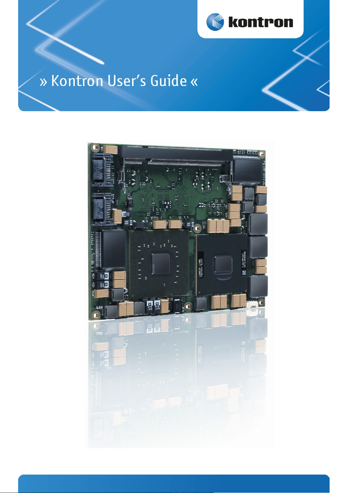
ETX®-CD
Document Revision 130
www.kontron.com
Page 2

Page 3

» Table of Contents «
1 User Information..................................................................................5
1.1 About This Document.................................................................................................................... 5
1.2 Copyright Notice.......................................................................................................................... 5
1.3 Trademarks................................................................................................................................. 5
1.4 Standards................................................................................................................................... 5
1.5 Warranty.................................................................................................................................... 6
1.6 Technical Support......................................................................................................................... 6
2 Introduction........................................................................................7
2.1 Product Description...................................................................................................................... 7
2.2 ETX® Documtentation................................................................................................................... 7
2.3 ETX® Benefits.............................................................................................................................. 8
3 Specification.......................................................................................9
3.1 Modules & Accessories................................................................................................................... 9
3.2 Functional Specification............................................................................................................... 10
3.3 Block Diagram............................................................................................................................ 13
3.4 Electrical Specification................................................................................................................ 14
3.4.1 Supply Voltage........................................................................................................................... 14
3.4.2 Power Supply Rise Time................................................................................................................ 14
3.4.3 Supply Voltage Ripple.................................................................................................................. 14
3.4.4 Power Consumption..................................................................................................................... 14
3.5 Environmental Specification......................................................................................................... 15
3.5.1 Temperature Specification............................................................................................................ 15
3.5.2 Humidity................................................................................................................................... 15
3.6 Standards and Certifications......................................................................................................... 16
3.7 MTBF........................................................................................................................................ 18
3.8 Mechanical Specification.............................................................................................................. 19
3.9 Module Drillhole Dimension.......................................................................................................... 19
3.10 Thermal Management.................................................................................................................. 20
3.11 Heatspreader............................................................................................................................. 20
3.12 Onboard Fan Connector................................................................................................................ 21
3.12.1 Electrical Characteristics.............................................................................................................. 23
4 Features and Interfaces.......................................................................24
4.1 LPC.......................................................................................................................................... 24
4.2 M.A.R.S.................................................................................................................................... 25
4.3 JIDA16 and JIDA32..................................................................................................................... 26
4.4 K-Station 1................................................................................................................................ 27
4.5 GPIO - General Purpose Input and Output.........................................................................................28
4.6 Watchdog Timer.......................................................................................................................... 29
4.7 Speedstep Technology................................................................................................................. 30
www.kontron.com
Page 4

ETX®-CD /
4.8 C-States.................................................................................................................................... 31
4.9 ACPI Suspend Modes and Resume Events..........................................................................................32
4.10 ISA Bus Limitation...................................................................................................................... 33
5 System Resources...............................................................................34
5.1 Interrupt Request (IRQ) Lines........................................................................................................ 34
5.2 Direct Memory Access (DMA) Channels............................................................................................. 36
5.3 Memory Area............................................................................................................................. 36
5.4 I/O Address Map......................................................................................................................... 36
5.5 Inter-IC (I2C) Bus....................................................................................................................... 36
5.6 System Management (SM) Bus....................................................................................................... 36
5.7 JILI-I2C Bus.............................................................................................................................. 36
6 ETX® Connectors................................................................................37
6.1 Connector Locations.................................................................................................................... 37
6.2 General Signal Description............................................................................................................ 37
6.3 Connector X1 (PCI bus, USB, Audio)................................................................................................ 38
6.3.1 Connector X1 Signal Levels........................................................................................................... 39
6.3.2 Connector X1 Signal Description..................................................................................................... 41
6.4 Connector X2 (ISA Bus)................................................................................................................ 42
6.4.1 Connector X2 Signal Levels........................................................................................................... 43
6.4.2 Connector X2 Signal Description.................................................................................................... 45
6.5 Connector X3 (VGA, LCD, Video, COM1 and COM2, LPT/Floppy, Mouse, Keyboard).......................................45
6.5.1 Connector X3 (Signal Levels).........................................................................................................47
6.5.2 Connector X3 Signal Description.................................................................................................... 49
6.6 Connector X4 Subsystems............................................................................................................. 51
6.6.1 Connector X4 (IDE 1, IDE 2, Ethernet, Miscellaneous).......................................................................... 51
6.6.2 Connector X4 (Signal Levels)......................................................................................................... 52
6.6.3 Connector X4 Signal Description.................................................................................................... 54
6.7 Feature Connector J11................................................................................................................. 56
6.7.1 SDVO Output.............................................................................................................................. 56
6.7.2 SDVO Connector and Flat Foil Cable.................................................................................................56
6.7.3 Pinout Feature Connector J11........................................................................................................ 56
7 BIOS Operation...................................................................................58
7.1 Determining the BIOS Version....................................................................................................... 58
7.1.1 Start Phoenix BIOS Setup Utility.................................................................................................... 58
7.2 BIOS Setup Menu........................................................................................................................ 60
7.2.1 Info Screen................................................................................................................................ 60
7.2.2 Main Menu................................................................................................................................. 61
7.2.3 Advanced.................................................................................................................................. 63
7.2.4 Security.................................................................................................................................... 82
7.2.5 Power....................................................................................................................................... 83
7.2.6 Boot........................................................................................................................................ 86
7.2.7 Exit Menu.................................................................................................................................. 87
4
Page 5

ETX®-CD / User Information
1 User Information
1.1 About This Document
This document provides information about products from Kontron Europe GmbH and/or its subsidiaries. No warranty of
suitability, purpose, or fitness is implied. While every attempt has been made to ensure that the information in this
document is accurate, the information contained within is supplied “as-is” and is subject to change without notice.
For the circuits, descriptions and tables indicated, Kontron assumes no responsibility as far as patents or other rights of
third parties are concerned.
1.2 Copyright Notice
Copyright © 2003-2012 Kontron Europe GmbH
All rights reserved. No part of this document may be reproduced, transmitted, transcribed, stored in a retrieval system, or
translated into any language or computer language, in any form or by any means (electronic, mechanical, photocopying,
recording, or otherwise), without the express written permission of Kontron Europe GmbH.
DIMM-PC®, PISA®, ETX®, ETXexpress®, microETXexpress®, X-board®, DIMM-IO® and DIMM-BUS® are trademarks or
registered trademarks of Kontron Europe GmbH. Kontron is trademark or registered trademark of Kontron AG.
1.3 Trademarks
The following lists the trademarks of components used in this board.
» IBM, XT, AT, PS/2 and Personal System/2 are trademarks of International Business Machines Corp.
» Microsoft is a registered trademark of Microsoft Corp.
» Intel is a registered trademark of Intel Corp.
» All other products and trademarks mentioned in this manual are trademarks of their respective owners.
1.4 Standards
Kontron Europe GmbH is certified to ISO 9000 standards.
5
Page 6

ETX®-CD / User Information
1.5 Warranty
This Kontron Europe GmbH product is warranted against defects in material and workmanship for the warranty period
from the date of shipment. During the warranty period, Kontron Europe GmbH will at its discretion decide to repair or
replace defective products.
Within the warranty period, the repair of products is free of charge as long as warranty conditions are observed.
The warranty does not apply to defects resulting from improper or inadequate maintenance or handling by the buyer,
unauthorized modification or misuse, operation outside of the product’s environmental specifications or improper
installation or maintenance.
Kontron Europe GmbH will not be responsible for any defects or damages to other products not supplied by Kontron
Europe GmbH that are caused by a faulty Kontron Europe GmbH product.
1.6 Technical Support
Technicians and engineers from Kontron Europe GmbH and/or its subsidiaries are available for technical support. We are
committed to making our product easy to use and will help you use our products in your systems.
Please consult our Web site at http://www.kontron.com/support for the latest product documentation, utilities, drivers
and support contacts. Consult our customer section http://emdcustomersection.kontron.com for the latest BIOS
downloads, Product Change Notifications, Board Support Packages, DemoImages, 3D drawings and additional tools and
software. In any case you can always contact your board supplier for technical support.
6
Page 7

ETX®-CD / Introduction
2 Introduction
2.1 Product Description
Based on the ETX® standard, Kontron’s ETX®-CD, powered by a variety of Intel Pentium core duo processors, is a nextgeneration embedded module that brings advanced technology to tomorrow’s applications, as well as continuing today’s
legacy devices. Built around serial differential signaling technologies, ETX®-CD modules incorporate the following
interfaces into a 95 x 114 small form factor embedded module:
» PCI
» 2x Serial ATA (SATA)
» 1x Parallel ATA (IDE)
» USB
» 2x Serial Port (COM)
» 1x Parallel Port (LPT) shared with Floppy
» LVDS, SDVO, VGA
» 10/100 MB Ethernet
» ISA bus
» Audio
» Advanced Configuration and Power Interface (ACPI)
The ETX®-CD is built around the Intel Core Duo processors that use the Yonah and Merom Core and the Mobile Intel
945GME Express chipset, which is the first mobile platform to offer PCI Express functionality with extended life cycle
support. These modules feature the most current desktop features such as USB, SATA, and PCI buses. The ETX®-CD delivers
up to 2GHz performance and up to 2GB DDR2 RAM. For applications that require advanced real-time video capabilities, the
ETX®-CD has integrated graphics based on the Intel® Graphics Media Accelerator 900 architecture. The ETX®-CD supports
4 PCI 32-bit PCI devices. A 10/100 megabits per second Ethernet port provides fast connectivity to LAN/WAN and 4x USB
interface provides fast and sufficient interfaces for external peripherals. ETX®-CD modules also provide the following
interfaces that are always located in the same physical position on each board: PCI32, USB, serial ATA (SATA), parallel ATA
(PATA), LVDS Multi Media ports, as well as an ACPI (Advanced Configuration and Power Interface) for optimized power
management are available on the board. Six mounting holes on the board provide secure mounting to allow the module
increased shock and vibration resistance.
2.2 ETX® Documtentation
This product manual serves as one of three principal references for an ETX® design. It documents the specifications and
features of ETX®-CD. The other two references, which are available from the Kontron Europe GmbH Web site, include:
» The ETX® Specification defines the ETX® module form factor, pinout, and signals.
» The ETX® Design Guide serves as a general guide for baseboard design, with a focus on maximum flexibility to
accommodate a wide range of ETX® modules.
Some of the information contained within this product manual applies only to certain
product revisions (CE: xxx). If certain information applies to specific product revisions (CE:
xxx) it will be stated. Please check the product revision of your module to see if this
information is applicable.
7
Page 8

ETX®-CD / Introduction
2.3 ETX® Benefits
Embedded technology extended (ETX) modules are very compact (114 x 95 mm), highly integrated computers. All ETX®
modules feature a standardized form factor and a standardized connector layout that carry a specified set of signals. This
standardization allows designers to create a single-system baseboard that can accept present and future ETX® modules.
ETX® modules include common personal computer (PC) peripheral functions such as:
» Graphics
» Parallel, Serial, and USB ports
» Keyboard/mouse
» Ethernet
» Sound
» IDE (and SATA)
The baseboard designer can optimize exactly how each of these functions implements physically. Designers can place
connectors precisely where needed for the application on a baseboard designed to optimally fit a system’s packaging.
Peripheral PCI or ISA buses can be implemented directly on the baseboard rather than on mechanically unwieldy
expansion cards. The ability to build a system on a single baseboard using the computer as one plug-in component
simplifies packaging, eliminates cabling, and significantly reduces system-level cost. A single baseboard design can use a
range of ETX® modules. This flexibility can differentiate products at various price/performance points, or to design future
proof systems that have a builtin upgrade path. The modularity of an ETX® solution also ensures against obsolescence as
computer technology evolves. A properly designed ETX® baseboard can work with several successive generations of ETX®
modules. An ETX® baseboard design has many advantages of a custom, computer-board design but delivers better
obsolescence protection, greatly reduced engineering effort, and faster time to market.
8
Page 9
ETX®-CD / Specification
3 Specification
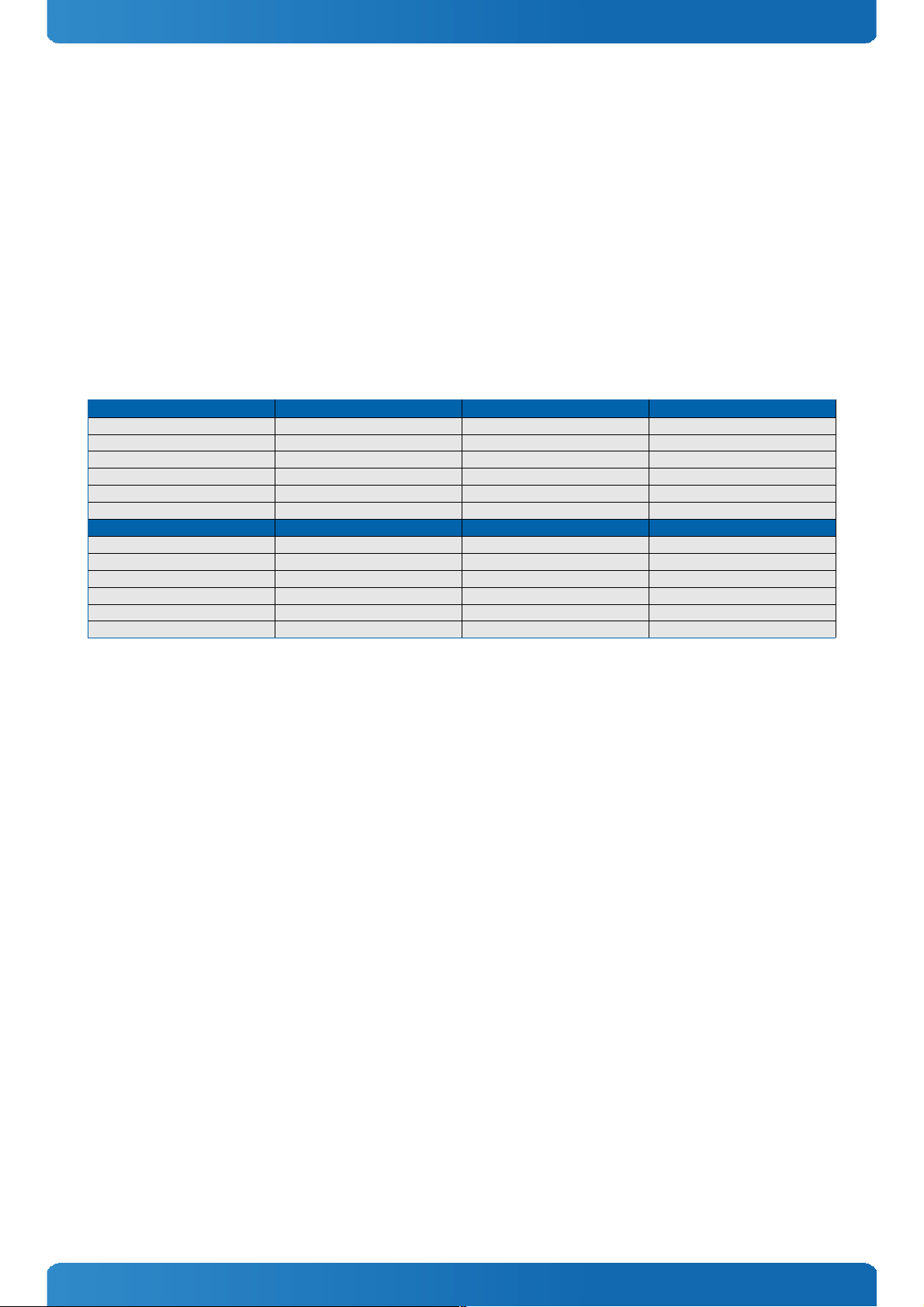
3.1 Modules & Accessories
The Computer-on-Module ETX®-CD (MCAL) based on Intel's Napa platform is available in different variants to cover the
demand of different performance, price and power:
Commercial grade modules (0°C to 60°C operating)
Product Number Product Name Processor Chipset and Features
18030-0000-11-4 ETX-CD 1.06GHz C423 Intel® Celeron® M ULV 423 Intel® 945GME, ICH7M
18030-0000-12-5 ETX-CD 1.2GHz U2500 Intel® Core™ Duo U2500 Intel® 945GME, ICH7M
18030-0000-15-6 ETX-CD 1.5GHz L7400 Intel® Core™ 2 Duo L7400 Intel® 945GME, ICH7M
18030-0000-17-5 ETX-CD 1.66GHz L2400 Intel® Core™ Duo L2400 Intel® 945GME, ICH7M
18030-0000-19-4 ETX-CD 1.86GHz C440 Intel® Celeron® M ULV 423 Intel® 945GME, ICH7M
Extended Temperature modules (-25°C to 75°C operating)
Product Number Product Name Processor Chipset and Features
18030-0000-17-5EXT ETX-CD 1.66GHz E1 Intel® Core™ Duo L2400 Intel® 945GME, ICH7M
18030-0000-11-4EXT ETX-CD 1.06GHz C423 E1 Intel® Celeron® M ULV 423 Intel® 945GME, ICH7M
Documentation is also valid for following End-of-Live (EOL) variants:
Product Number Product Name Processor Chipset and Features
18030-0000-11-1 ETX-CD 1.06GHz Intel® Celeron® M ULV 423 Intel® 945GM, ICH7M
18030-0000-11-1EXT ETX-CD 1.06GHz E1 Intel® Celeron® M ULV 423 Intel® 945GM, ICH7M
18030-0000-12-2 ETX-CD 1.2GHz Intel® Core™ Duo U2500 Intel® 945GM, ICH7M
18030-0000-15-3 ETX-CD 1.5GHz Intel® Core™ 2 Duo L7400 Intel® 945GM, ICH7M
18030-0000-17-2 ETX-CD 1.66GHz Intel® Core™ Duo L2400 Intel® 945GM, ICH7M
18030-0000-17-2EXT ETX-CD 1.66GHz E1 Intel® Core™ Duo L2400 Intel® 945GM, ICH7M
Accessories
Product Number Product Name
18010-0000-00-0 ETX® Eval (ADA8)
18028-0000-00-0 ETX® miniBaseboard (ADAB)
97011-5120-08-0 DDR2-800 SODIMM / 512MB
97011-1024-08-0 DDR2-800 SODIMM / 1GB
97011-2048-08-0 DDR2-800 SODIMM / 2GB
97011-5120-08-2 DDR2-800 SODIMM / 512MB E2 (industrial temperature)
97011-1024-08-2 DDR2-800 SODIMM / 1GB E2 (industrial temperature)
97011-2048-08-2 DDR2-800 SODIMM / 2GB E2 (industrial temperature)
18030-0000-99-0 ETX®-CD, Heatspreader, threaded
18030-0000-99-1 ETX®-CD, Heatspreader, through hole
18030-0000-99-0C01 ETX®-CD, Passive Cooling Solution, threaded
18030-0000-99-0CO2 ETX®-CD, Active Cooling Solution, threaded
96006-0000-00-4 ADA-ETX-CD-FC4 (SDVO FFC45 to 2xDVI Adaptor)
96006-0000-00-5 ADA-SDVOB-FC5 (SDVO FFC45 to 1xDVI Adaptor)
96006-0000-00-6 ADA-SDVOB-LVDS (SDVO FFC45 to LVDS Adaptor)
9-5000-0352 ADA-LVDS-DVI 18bit (LVDS to DVI converter)
9-5000-0353 ADA-LVDS-DVI 24bit (LVDS to DVI converter)
96079-0000-00-0 KAB-HSP 200mm (Cable adapter to connect FAN to module)
96079-0000-00-2 KAB-HSP 40mm (Cable adapter to connect FAN to module)
9
Page 10
ETX®-CD / Specification
3.2 Functional Specification
Processor
The Intel® Core™ Duo / Celeron® (Yonah / Merom) CPU supports:
» Intel® Hyper-Threading Technology (HTT)
» Enhanced Intel SpeedStep® Technology (EIST)
» Thermal Monitoring Technologies
» Idle States (C-States)
» Execute Disable Bit
Processor # of Cores Lithography Core Core Clock L2 Cache VT-x HT Intel® 64 EIST Max TDP
Intel® Celeron® M ULV 423 1 65nm Yonah 1066 MHz 1MB No No No No 5.5W
Intel® Celeron® M 440 1 65nm Yonah 1866 MHz 1MB No No No No 27W
Intel® Core™ Duo U2500 2 65nm Yonah 1200 MHz 2MB Yes No No Yes 9W
Intel® Core™ Duo L2400 2 65nm Yonah 1666 MHz 2MB Yes No No Yes 15W
Intel® Core™ 2 Duo L7400 2 65nm Merom 1500 MHz 4MB Yes No No Yes 17W
Chipset
Chipset Graphic Outputs
82945GM VGA, SDVO, LVDS, TVout
82945GME VGA, SDVO, LVDS
Memory
Sockets
1x DDR2 SO-DIMM
Memory Type
DDR2-533, DDR2-667
Maximum Size
2GB
Technology
Single Channel
Graphics Core
The integrated Intel® GMA950 (Gen3.5) supports:
Graphics Core Render Clock
250 MHz
Execution Units / Pixel Pipelines
4
Max Graphics Memory
256MB
GFX Memory Bandwidth (GB/s)
10.7
GFX Memory Technology
DVMT 3.0
API (DirectX/OpenGL)
9.0c / 1.4
Shader Model
3.0 (SW) / 2.0
Hardware accelerated Video
-
Independent/Simultaneous Displays
2
Display Interfaces
CRT max Resolution
2048x1536
TV out:
YES
Digital Display:
SDVOB and SDVOC (onboard FFC45)
LVDS
LVDS Bits/Pixel
1x18, 2x18
LVDS Bits/Pixel with dithering
1x24 and 2x24
LVDS max Resolution:
1600x1200
PWM Backlight Control:
-
10
Page 11
ETX®-CD / Specification
Chipset & IOH
# of USB:
4x USB 1.1/2.0
USB onboard Connector:
-
Audio:
Crystal CS4299 / Via VT1612 AC97 Audio
PCI Bus:
PCI Rev 2.3 (33MHz/3.3V)
ISA Bus:
LPC2ISA Fintek F85226FG
SuperI/O Controller
Winbond 83627HFJ LPC-I/O
COM Ports:
2x RS232
IrDA Support:
IrDA 1.0 (SIR) or ASK-IrDA (COM2)
LPT Support:
EPP, ECP, bi-dir.
Max TDP:
7W + 3.3W
Storage
Primary IDE:
PATA 100
Secondary IDE:
-
SATA onboard connector:
2x SATA 1.5Gb/s
SATA features:
NCQ, HotPlug, Staggered Spinup
SATA RAID support:
-
onboard SSD:
-
onboard CF Card:
-
Onboard devices
Audio
Crystal CS4299 / Via VT1612 AC97 Audio
Trusted Platform Module
STMicro ST19WP18 optional
Ethernet
The Intel 82562GZ ethernet supports:
» Jumbo Frames
» Time Sync Protocol Indicator
» WOL (Wake On LAN)
» PXE (Preboot eXecution Environment)
Kontron Features
I2C/SMB support:
YES/YES
M.A.R.S. support
YES
Embedded API
JIDA16 / JIDA32
JIDA32 Applications / K-Station
YES, K-Station 1 w/o BIOS modification
Custom BIOS Settings / Flash Backup
-
Watchdog support
YES
11
Page 12
ETX®-CD / Specification
Power Features
ACPI
ACPI 1.0b / 2.0
S-States
S0, S1, S3, S4, S5
Graphic States
D0, D3
Misc Power Management
DPST 2.0
Power Consumption and Performance
Full Load Power Consumption
19 - 40W
Kontron Performance Index
1387-3296
Kontron Performance/Watt
71 - 103
Detailed Power Consumption measurements in all states and bechmarks for CPU, Graphics
and Memory performance are available in Application Note KEMAP054 at EMD Customer
Section.
Supported Operating Systems
The ETX®-CD currently supports:
» Microsoft Windows XP x86
» Microsoft Windows 7 x86
» Microsoft Windows CE 6.0
» Microsoft Windows XP embedded
» Linux
» WindRiver VxWorks
12
Page 13
ETX®-CD / Specification
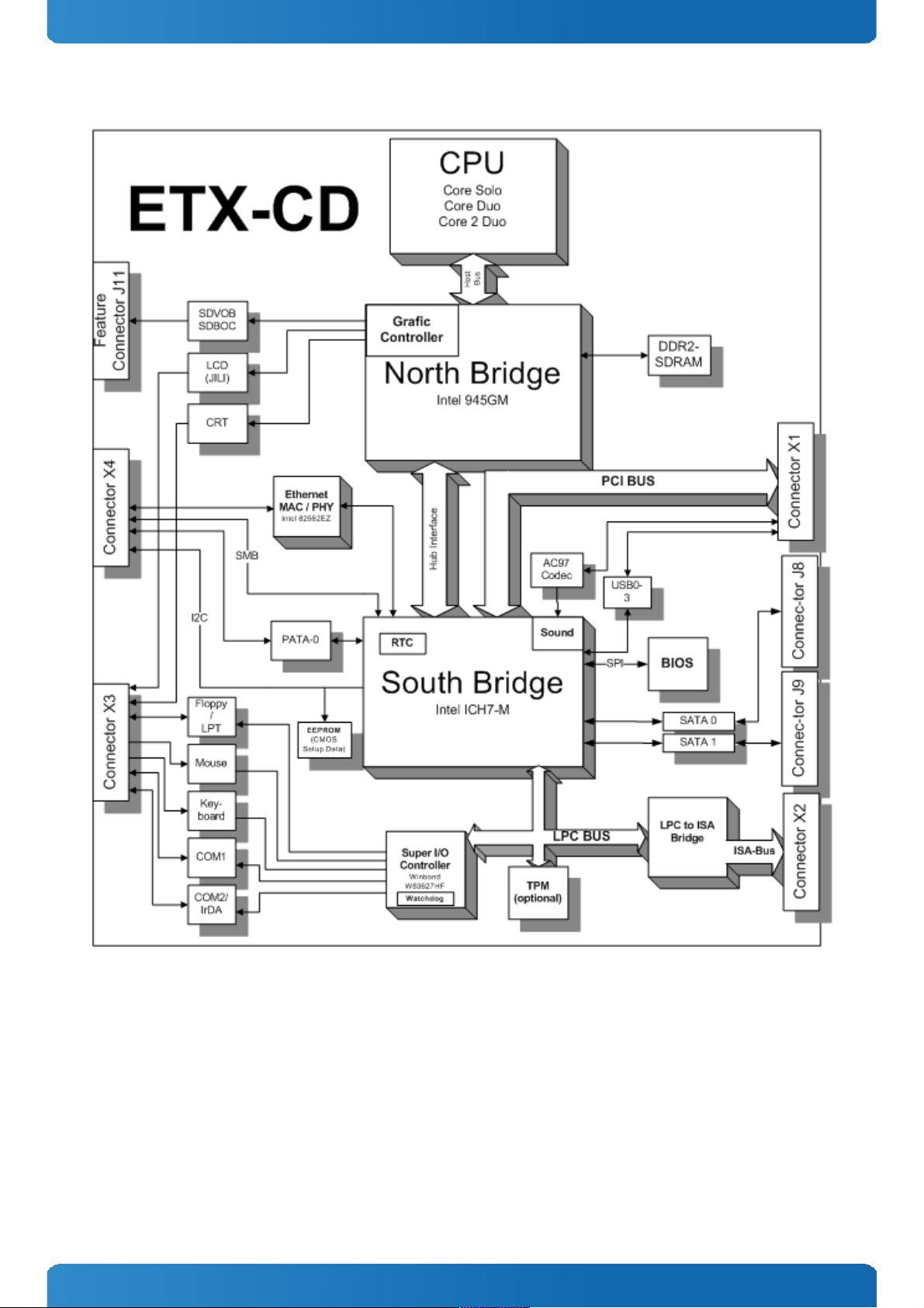
3.3 Block Diagram
13
Page 14

ETX®-CD / Specification
3.4 Electrical Specification
3.4.1 Supply Voltage
Following supply voltage is specified at the ETX® connector:
Supply Voltage:
5V +/- 5%
5V_Stb:
5V DC +/- 5%
3.4.2 Power Supply Rise Time
» The input voltages shall rise from ≤10% of nominal to within the regulation ranges within 0.1ms to 20ms.
» There must be a smooth and continuous ramp of each DC input voltage from 10% to 90% of its final set-point
following the ATX specification
3.4.3 Supply Voltage Ripple
» Maximum 100 mV peak to peak 0 – 20 MHz
3.4.4 Power Consumption
The maximum Power Consumption of the different ETX®-CD modules is 19 - 40W (100% CPU load; 90°C CPU temperature).
Further details with measurements and TDP values of the single variants can be found in our customer section.
Information there is available after registration.
14
Page 15
ETX®-CD / Specification
3.5 Environmental Specification
3.5.1 Temperature Specification
General Kontron Specification Operating Non-operating
Commercial grade 0°C to +60°C -30°C to +85°C
Extended Temperature(E1) -25°C to +75°C -30°C to +85°C
Industrial grade by Screening (XT) -40°C to +85°C -40°C to +85°C
Industrial grade by Design (E2) -40°C to +85°C -40°C to +85°C
Please see chapter Product Specification for available variants for extended or industrial
temperate grade
With Kontron heatspreader plate assembly
The operating temperature defines two requirements:
» the maximum ambient temperature with ambient being the air surrounding the module.
» the maximum measurable temperature on any spot on the heatspreader's surface
Without Kontron heatspreader plate assembly
The operating temperature is the maximum measurable temperature on any spot on the module's surface.
3.5.2 Humidity
» 93% relative Humidity at 40°C, non-condensing (according to IEC 60068-2-78)
15
Page 16

ETX®-CD / Specification
3.6 Standards and Certifications
RoHS
The ETX®-CD is compliant to the directive 2002/95/EC on the restriction of the use of certain hazardous substances
(RoHS) in electrical and electronic equipment.
CE marking
The ETX®-CD is CE marked according to Low Voltage Directive 2006/95/EC – Test standard EN60950
Component Recognition UL 60950-1
The ETX® form factor Computer-on-Modules are Recognized by Underwriters Laboratories Inc. Representative samples of
this component have been evaluated by UL and meet applicable UL requirements.
UL Listings:
» NWGQ2.E304278
» NWGQ8.E304278
WEEE Directive
WEEE Directive 2002/96/EC is not applicable for Computer-on-Modules.
Conformal Coating
Conformal Coating is available for Kontron Computer-on-Modules and for validated SO-DIMM memory modules. Please
contact your local sales or support for further details.
16
Page 17

ETX®-CD / Specification
Shock & Vibration
The ETX® form factor Computer-on-Modules successfully passed shock and vibration tests according to
» IEC/EN 60068-2-6 (Non operating Vibration, sinusoidal, 10Hz-4000Hz, +/-0.15mm, 2g)
» IEC/EN 60068-2-27 (Non operating Shock Test, half-sinusoidal, 11ms, 15g)
EMC
Validated in Kontron reference housing for EMC the ETX®-CD follows the requirements for electromagnetic compatibility
standards
» EN55022
17
Page 18
ETX®-CD / Specification
3.7 MTBF
The following MTBF (Mean Time Before Failure) values were calculated using a combination of manufacturer’s test data, if
the data was available, and the Telcordia (Bellcore) issue 2 calculation for the remaining parts.
The calculation methode used is “Bellcore Method 1 Case 1” in a ground benign, controlled environment (GB,GC). This
particular method takes into account varying temperature and stress data and the system is assumed to have not been
burned in.
Other environmental stresses (extreme altitude, vibration, salt water exposure, etc) lower MTBF values.
System MTBF (hours): 109418 @ 40°C
Fans usually shipped with Kontron Europe GmbH products have 50,000-hour typical
operating life. The above estimates assume no fan, but a passive heat sinking arrangement
Estimated RTC battery life (as opposed to battery failures) is not accounted for in the above
figures and need to be considered for separately. Battery life depends on both temperature
and operating conditions. When the Kontron unit has external power; the only battery
drain is from leakage paths.
18
Page 19
ETX®-CD / Specification
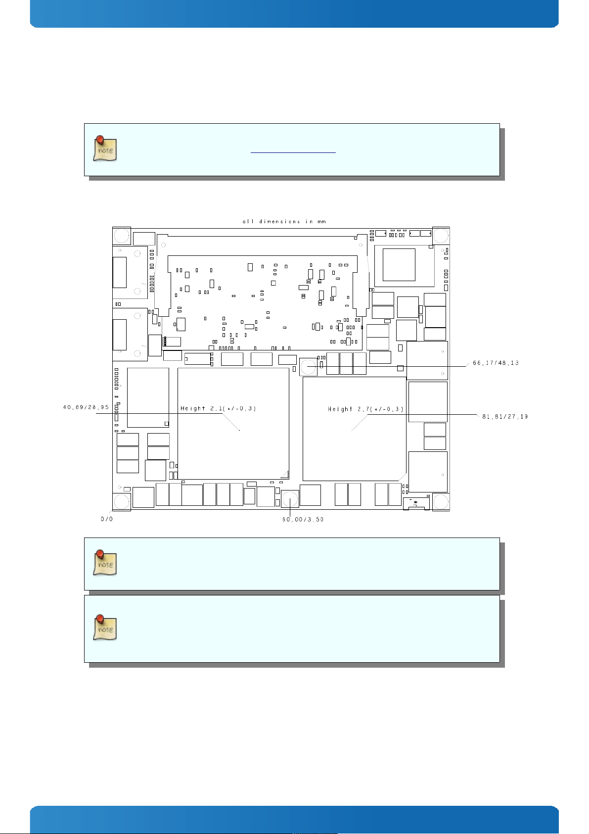
3.8 Mechanical Specification
» 95.0 mm x 114.0 mm
» Hight approx. 12mm (0.4”)
CAD drawings are available at EMD CustomerSection
3.9 Module Drillhole Dimension
The not shown drill holes match with the ETX® specification.
The maximum height of electrical components on the bottom side of the module is
specified with 2.0mm in the ETX@ specification. On the ETX@-CD the Southbridge is
soldered on the bottom side and Intel specified the ICH7 with 2.28mm ± 0.21mm
19
Page 20

ETX®-CD / Specification
3.10 Thermal Management
A heatspreader plate assembly is available from Kontron Europe GmbH for the ETX®-CD. The heatspreader plate on top of
this assembly is NOT a heat sink. It works as a ETX®-standard thermal interface to use with a heat sink or other cooling
device.
External cooling must be provided to maintain the heatspreader plate at proper operating temperatures. Under worstcase conditions, the cooling mechanism must maintain an ambient air and heatspreader plate temperature of 60° C or
less.
The aluminum slugs and thermal pads on the underside of the heatspreader assembly implement thermal interfaces
between the heatspreader plate and the major heat-generating components on the ETX®-CD. About 80 percent of the
power dissipated within the module is conducted to the heatspreader plate and can be removed by the cooling solution.
You can use many thermal-management solutions with the heatspreader plates, including active and passive approaches.
The optimum cooling solution varies, depending on the ETX® application and environmental conditions. Please see the
ETX® Design Guide for further information on thermal management.
3.11 Heatspreader
Documentation and CAD drawings of ETX®-CD heatspreader and cooling solutions is provided at
http://emdcustomersection.kontron.com.
20
Page 21
ETX®-CD / Specification
3.12 Onboard Fan Connector
This section describes how to connect a fan to the connector located directly on the ETX®-CD. With certain BIOS-settings
it is possible to control the fan depending on the Active Trip Point temperature. The fan switches on/off depending on the
adjusted Active Trip Point temperature. In order for this feature to function properly an ACPI compliant OS is necessary.
The ETX® CD can not control the revolutions per minute (R.P.M) of the fan.
Location and Pinout of Fan Connector
21
Page 22
ETX®-CD / Specification
The onboard fan connector (J6) can be found near the northbridge at the corner of the module.
Connector J1 has following specification:
» Part number (Molex) J8: 53261-0390
» Mates with: 51021-0300
» Crimp terminals: 50079-8100
The Pin assignement is:
» Pin1: Tacho
» Pin2: VCC
» Pin3: GND
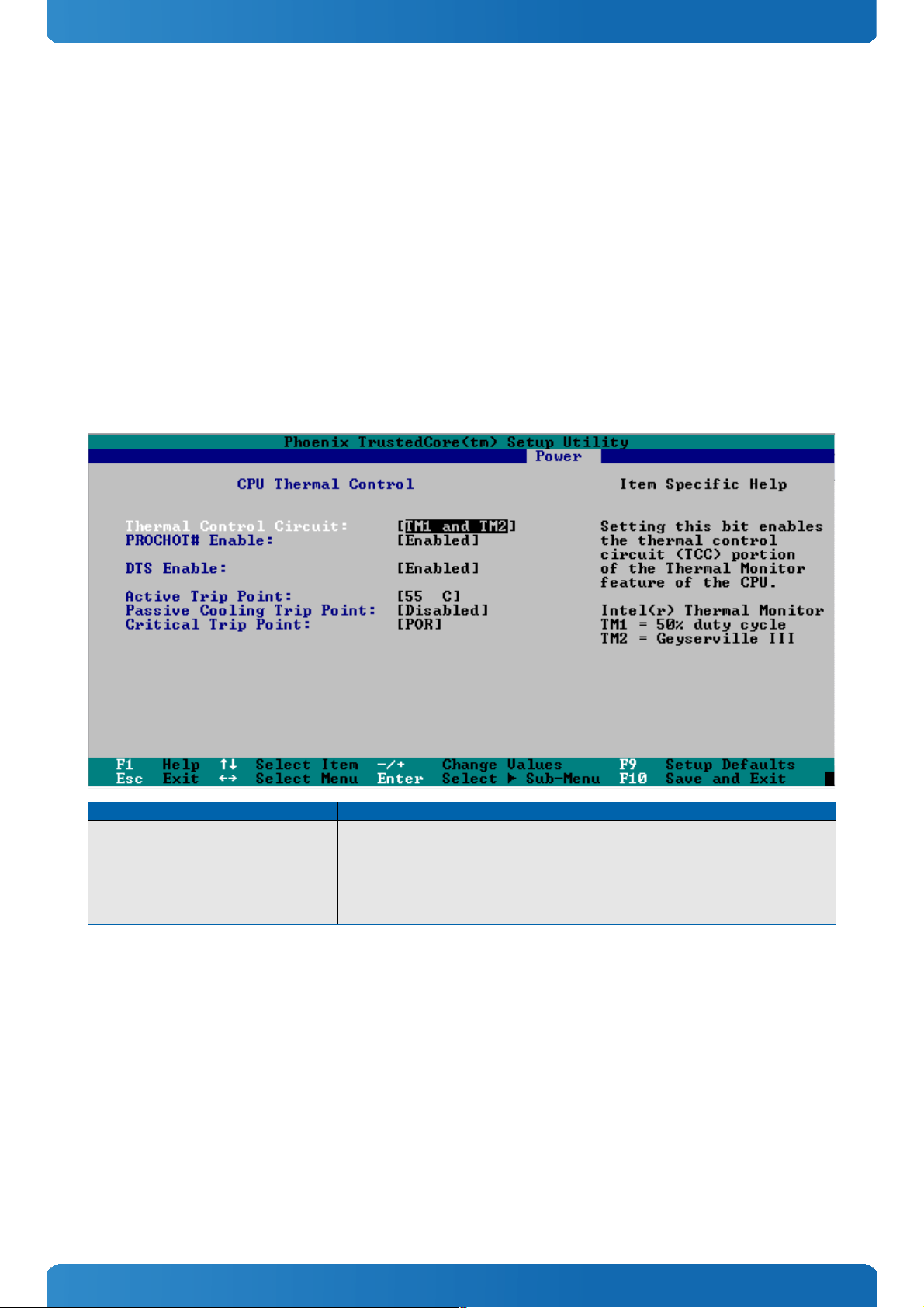
BIOS Settings for Fan Control
The fan can be controlled via the BIOS Settings “Power Thermal Control”→
Feature Option Description
Active Trip Point Disabled
15 C
23 C
…
55 C
63 C
…
119 C
This value controls the temperature of the ACPI active
trip point - the point in which the OS will turn on the
CPU fan (connector on PCB). If DTS is enabled only
values below 97°C are valid.
22
Page 23
ETX®-CD / Specification
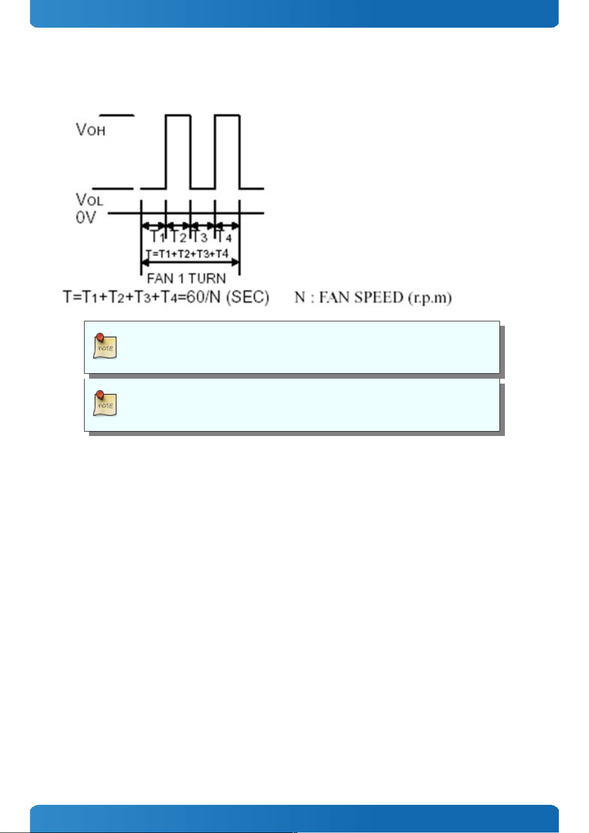
3.12.1 Electrical Characteristics
Vcc = 5 V Imax (continuous) = 0,68 A Imax (pulsed) = 2 A Sense (Tacho-pulse) = 4 Pulses per turn
The 5 V output is not short circuit proof. The user has to ensure that the circuit is protected
externally, for example by a fuse on the backplane.
To connect a standard FAN with 3pin connector to the module please use adaptor cable
KAB-HSP 200mm (96079-0000-00-0) or KAB-HSP 40mm (96079-0000-00-2)
23
Page 24
ETX®-CD / Features and Interfaces
4 Features and Interfaces
4.1 LPC
The Low Pin Count (LPC) Interface signals are connected to the LPC Bus bridge located in the CPU or chipset. The LPC low
speed interface can be used for peripheral circuits such as an external Super I/O Controller, which typically combines
legacy-device support into a single IC. The implementation of this subsystem complies with the COM Express®
Specification. Implementation information is provided in the COM Express® Design Guide maintained by PICMG. Please
refer to the official PICMG documentation for additional information.
The LPC bus does not support DMA (Direct Memory Access) and a clock buffer is required when more than one device is
used on LPC. This leads to limitations for ISA bus and SIO (standard I/O´s like Floppy or LPT interfaces) implementations.
All Kontron COM Express® Computer-on-Modules imply BIOS support for following external baseboard LPC Super I/O
controller features for the Winbond/Nuvoton 5V 83627HF/G and 3.3V 83627DHG-P:
83627HF/G Phoenix BIOS AMI CORE8 AMI Aptio
PS/2 YES YES YES
COM1/COM2 YES YES YES
LPT YES YES YES
HWM YES YES NO
Floppy NO NO NO
GPIO NO NO NO
83627DHG-P Phoenix BIOS AMI CORE8 AMI Aptio
PS/2 YES YES YES
COM1/COM2 YES YES YES
LPT YES YES YES
HWM NO NO NO
Floppy NO NO NO
GPIO NO NO NO
Features marked as not supported do not exclude OS support (e.g. HWM can be accessed via SMB). For any other LPC
Super I/O additional BIOS implementations are necessary. Please contact your local sales or support for further details.
24
Page 25

ETX®-CD / Features and Interfaces
4.2 M.A.R.S.
The Smart Battery implementation for Kontron Computer-on-Modules called Mobile Application for Rechargeable Systems
is a BIOS extension for external Smart Battery Manager or Charger. It includes support for SMBus charger/selector (e.g.
Linear Technology LTC1760 Dual Smart Battery System Manager) and provides ACPI compatibility to report battery
information to the Operating System.
Reserved SM-Bus addresses for Smart Battery Solutions on the carrier:
8-bit Address 7-bit Address Device
12h 0x09 SMART_CHARGER
14h 0x0A SMART_SELECTOR
16h 0x0B SMART_BATTERY
25
Page 26
ETX®-CD / Features and Interfaces
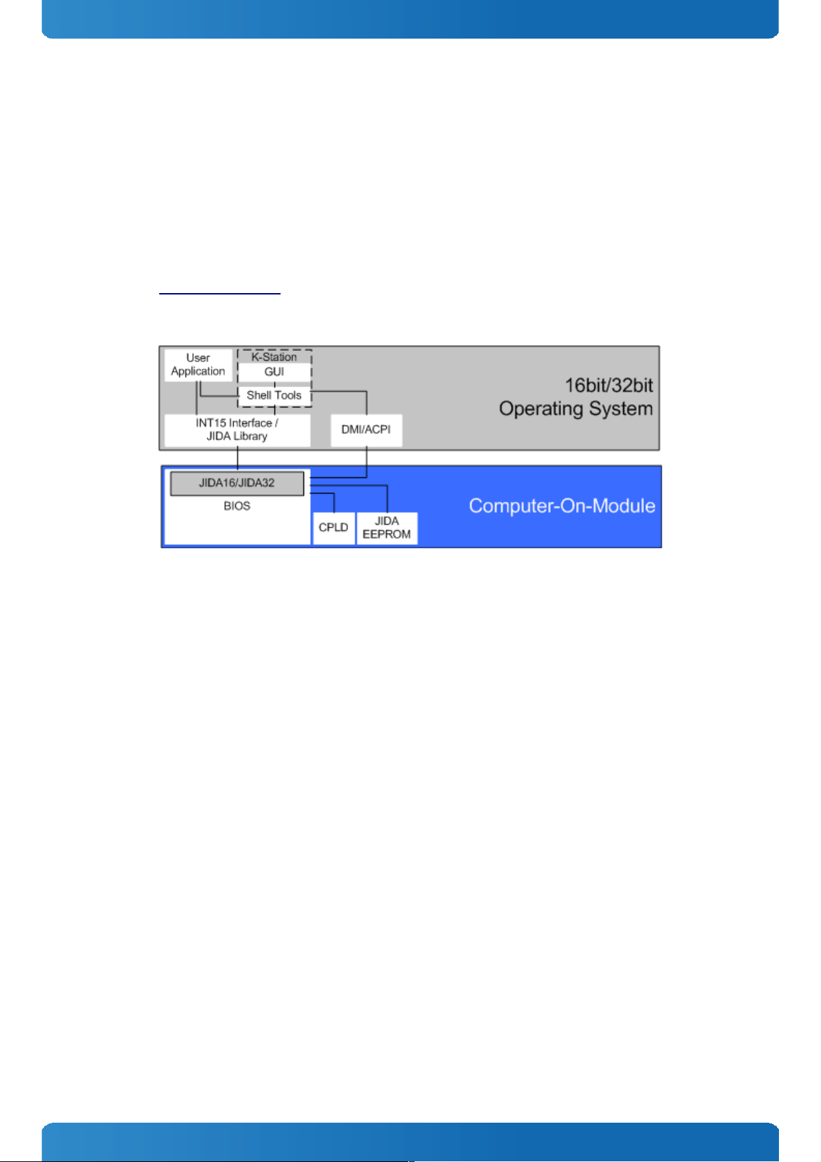
4.3 JIDA16 and JIDA32
JIDA16 (JUMPtec® Intelligent Device Architecture) is a BIOS interface which allows programs running in Real Mode
operating systems (i.e. MS DOS) to call certain functions implemented in the BIOS. These functions can be used to get
module information, make settings and access the I2C Bus and the Watchdog unit. JIDA16 functions are INT 15h BIOS calls
which are only available in 16 Bit Real Mode operating systems.
For 32bit operating systems (i.e. WindowsXP, Windows 7, Windows CE, VxWorks, Linux) a different JIDA implementation
called JIDA32 is implemented. The same common driver for all JIDA32 capable modules talks to the JIDA32 part in the
BIOS, which is hardware dependent to interact with the hardware.
Please refer to EMD Customer Section for detailed documentation, JIDA utilities and Libraries for DOS, Windows, Linux,
VxWorks or QNX.
Usage of JIDA16 and JIDA32
26
Page 27

ETX®-CD / Features and Interfaces
4.4 K-Station 1
Based on the JIDA32 interface users can implement advanced board functionality in their application. As an example
utility Kontron provides K-Station for most 32bit Windows Operating Systems. K-Station 1 is a summary of command line
utilities (Shell Tools) for easy access to JIDA32 BIOS implementations. Second part of K-Station is a JAVA based example
GUI which gives a view an all available features using the Shell Tools.
Following K-Station Shell Tools are available:
» KSystemSummary.exe (System Information)
» KGenInfo.exe (Module Information)
» KCPUPerf.exe (CPU Throttling control)
» KHWMon.exe (Hardware Monitoring)
» KI2CBus.exe (I2C and SMBus access)
» KIOPort.exe (GPIO control)
» KStorage.exe (JIDA EEPROM access to user bytes)
» KVGATool.exe (LVDS Backlight control)
» KWDog.exe (Watchdog control)
» KAMIMod.exe (AMICore8 BIOS Modification with Bootlogo or Usercode …)
» KFlash.exe (AMICore8 BIOS Update)
The full K-Station package, the stand-alone Shell Tools with drivers, example batch files and documentation is available
on EMD Customer Section for free.
27
Page 28

ETX®-CD / Features and Interfaces
4.5 GPIO - General Purpose Input and Output
The offers 4 General Purpose Input (GPI) pins and 4 General Purpose Output (GPO) pins. On a 3.3V level digital in- and
outputs are available.
Signal Pin Description
GPI0 A54 General Purpose Input 0
GPI1 A63 General Purpose Input 1
GPI2 A67 General Purpose Input 2
GPI3 A85 General Purpose Input 3
GPO0 A93 General Purpose Output 0
GPO1 B54 General Purpose Output 1
GPO2 B57 General Purpose Output 2
GPO3 B63 General Purpose Output 3
Configuration
The GPI and GPO pins can be configured via JIDA32/K-Station. Please refer to the JIDA32/K-Station manual in the driver
download packet on our customer section.
To enable GPIO functionality, modules with HW revision CE 1.x.x must be reworked. Contact
your local sales or support for further information. On modules with HW revision CE 4.x.x
and BIOS R115 or newer GPIO/SDIO can be switched via BIOS setup option
The General Purpose Inputs and Outputs are not applicable to drive applications faster than
2ms. It’s recommended to use data transfer rates only up to 1 kHz.
General Purpose Outputs are high impedance until first write access
There is one IO Port controlled via onboard CPLD (1 Byte, Port 0) available and the 4 Inputs and 4 Outputs are fixed in
direction. To access the GPIOs use the JIDA32 interface. You can write to a General Purpose Output with the upper half
byte. To read a General purpose Input use the lower half byte.
Bit of GPIO Port0 Function COM Express Pin
0 GPI0 A54
1 GPI1 A63
2 GPI2 A67
3 GPI3 A85
4 GPO0 A93
5 GPO1 B54
6 GPO2 B57
7 GPO3 B63
28
Page 29

ETX®-CD / Features and Interfaces
4.6 Watchdog Timer
You can configure the Watchdog Timer (WDT) in BIOS setup to start after a set amount of time after power-on boot. The
WDT can also be controlled by the JIDA32 Library API. The application software should strobe the WDT to prevent its
timeout. Upon timeout, the WDT resets and restarts the system. This provides a way to recover from program crashes or
lockups.
Configuration
You can program the timeout period for the watchdog timer in two ranges:
» 1-second increments from 1 to 255 seconds
» 1-minute increments from 1 to 255 minutes
Contact Kontron Embedded Modules technical support for information on programming and operating the WDT.
29
Page 30

ETX®-CD / Features and Interfaces
4.7 Speedstep Technology
The Intel® processors offers the Intel® Enhanced SpeedStep™ technology that automatically switches between maximum
performance mode and battery-optimized mode, depending on the needs of the application being run. It let you
customize high performance computing on your applications. When powered by a battery or running in idle mode, the
processor drops to lower frequencies (by changing the CPU ratios) and voltage, conserving battery life while maintaining
a high level of performance. The frequency is set back automatically to the high frequency, allowing you to customize
performance.
In order to use the Intel® Enhanced SpeedStep™ technology the operating system must support SpeedStep™ technology.
By disabling the SpeedStep feature in the BIOS, manual control/modification of CPU performance is possible. Setup the
CPU Performance State in the BIOS Setup or use 3rd party software to control CPU Performance States.
30
Page 31

ETX®-CD / Features and Interfaces
4.8 C-States
New generation platforms include power saving features like SuperLFM, EIST (P-States) or C-States in O/S idle mode.
Activated C-States are able to dramatically decrease power consumption in idle mode by reducing the Core Voltage or
switching of parts of the CPU Core, the Core Clocks or the CPU Cache.
Following C-States are defined:
C-State Description Function
C0 Operating CPU fully turned on
C1 Halt State Stops CPU main internal clocks via software
C1E Enhanced Halt Similar to C1, additionally reduces CPU voltage
C2 Stop Grant Stops CPU internal and external clocks via hardware
C2E Extended Stop Grant Similar to C2, additionally reduces CPU voltage
C3 Deep Sleep Stops all CPU internal and external clocks
C3E Extended Stop Grant Similar to C3, additionally reduces CPU voltage
C4 Deeper Sleep Reduces CPU voltage
C4E Enhanced Deeper Sleep Reduces CPU voltage even more and turns off the memory cache
C6 Deep Power Down Reduces the CPU internal voltage to any value, including 0V
C7 Deep Power Down Similar to C6, additionally LLC (LastLevelCache) is switched off
C-States are usually enabled by default for low power consumption, but active C-States my influence performance
sensitive applications or real-time systems.
» Active C6-State may influence data transfer on external Serial Ports
» Active C7-State may cause lower CPU and Graphics performance
It's recommended to disable C-States / Enhanced C-States in BIOS Setup if any problems occur.
31
Page 32

ETX®-CD / Features and Interfaces
4.9 ACPI Suspend Modes and Resume Events
The ETX®-CD supports the S3 state (=Save to Ram). S4 (=Save to Disk) is not supported by the BIOS (S4_BIOS) but S4_OS
is supported by the following operating systems:
» Windows XP
» Windows Vista
» Windows 7
The following events resume the system from S3:
» USB Keyboard (1)
» USB Mouse (1)
» Power Button
» WakeOnLan (2)
The following events resume the system from S4:
» Power Button
» WakeOnLan (2)
The following events resume the system from S5:
» Power Button
» WakeOnLan (2)
(1) OS must support wake up via USB devices and baseboard must power the USB Port with
StBy-Voltage
(2) WakeOnLan must be enabled in BIOS setup and driver options
32
Page 33

ETX®-CD / Features and Interfaces
4.10 ISA Bus Limitation
Memory accesses are not supported on the ISA bus. I/O accesses are only supported if they fall into one of the 4 generic
decode ranges provided by the chipset. If a plugin ISA card is using registers in I/O space, this address range has to be
enabled explicitely using the decode range and size setup items provided under the menu “Advanced” “Advanced→
Chipset Control” “ISA Options”. →
The following devices may also consume a generic decode range which can no longer be used for plugin cards. “Advanced”
“I/O device Configuration” “SIO Options”→ →
» “External SIO”: SIO2 config space, if this range is released (item set to disabled), none of the devices in the
external SIO will work
» Serial Port C/D: consumes one range if either one or both COMs are enabled
» External LPT: Consumes one range if enabled
“Advanced” “Hardware Monitor”→
» “Hardware Monitor”: consumes one range if enabled, disable if you don't require HWM support.
the BIOS doesn't check the range and size values set in the ISA Options menu. Ensure that
theses values do not conflict with other legacy and PCI I/O resources. Resource conflicts
may render the board inoperable.
If the number of generic decode ranges is exhausted, a conflict marker will be displayed
33
Page 34

ETX®-CD / System Resources
5 System Resources
5.1 Interrupt Request (IRQ) Lines
In 8259 PIC mode:
IRQ # Used For Available Comment
0 Timer0 No
1 Keyboard No
2 Slave 8259 No
3 COM2 No Note (1)
4 COM1 No Note (1)
5 LPT2 Yes Note (2)
6 Floppy Drive Controller No Note (1)
7 LPT1 No Note (1)
8 RTC No
9 SCI No
10 COM3 Yes Note (2)
11 COM4 Yes Note (2)
12 PS/2 Mouse No Note (1)
13 FPU No
14 IDE0 No Note (1)
15 SATA No Note (3)
1 If the “Used For” device is disabled in setup, the corresponding interrupt is available for
other devices.
2 Unavailable if baseboard is equipped with an I/O controller SMC FDC37C669, and the
device is enabled in setup.
3 Unavailable in SATA legacy mode. It cannot be used for PCI, but for ISA bus, when SATA is
in enhanced mode.
34
Page 35

ETX®-CD / System Resources
In APIC mode:
IRQ # Used For Available Available for PCI Comment
0 Timer0 No No
1 Keyboard No No
2 Slave 8259 No No
3 COM2 No Yes Note (1)
4 COM1 No Yes Note (1)
5 PCI/LPT2 Yes Yes Note (2)
6 Floppy Drive Controller No Yes Note (1)
7 LPT1 No Yes Note (1)
8 RTC No No
9 SCI No No System Control Interrupt (3)
10 COM3 Yes Yes Note (2)
11 COM4 Yes Yes Note (2)
12 PS/2 Mouse No Yes Note (1)
13 FPU No No
14 IDE0 No No
15 SATA No No Note (3)
16 PIRQ[A] For PCI PCI IRQ line 1 + USB UHCI
controller #0 + Graphics
controller
17 PIRQ[B] For PCI PCI IRQ line 2 + AC97 Audio
controller + USB UHCI controller
#1
18 PIRQ[C] For PCI PCI IRQ line 3 + USB UHCI
controller #2 + Native IDE
19 PIRQ[D] For PCI PCI IRQ line 4 + USB UHCI
controller #3
20 PIRQ[E] No Lan Controller
21 PIRQ[F] No
22 PIRQ[G] No
23 PIRQ[H] No USB EHCI controller
1 If the “Used For” device is disabled in setup, the corresponding interrupt is available for
other devices.
2 Unavailable if baseboard is equipped with an I/O controller SMC FDC37C669, and the
device is enabled in setup.
3 Unavailable in SATA legacy mode. It cannot be used for PCI, but for ISA bus, when SATA is
in enhanced mode.
The ETX®-CD is always booting in PIC mode. This might lead to the fact, that there are no
interrupts for PCI devices available when all onboard and SuperI/O interfaces are enabled.
Then the system stops without booting. The only solution is to deactivate interfaces.
35
Page 36

ETX®-CD / System Resources
5.2 Direct Memory Access (DMA) Channels
DMA # Used for Available Comment
0 Yes
1 Yes
2 FDC No If the “used-for” device is disabled in setup, the corresponding DMA channel
is available for other devices.
3 LPT Yes Unavailable if LPT is used in ECP mode.
4 Cascade No
5 Yes
6 Yes
7 Yes
5.3 Memory Area
Upper Memory Used for Available Comment
C0000h – CFFFFh VGA BIOS No
D0000h – DDFFFh Yes shadow RAM (ISA bus restriction)
DE000h – DFFFFh USB registers No
E0000h – FFFFFh System BIOS No
5.4 I/O Address Map
The I/O-port addresses of the ETX®-CD are functionally identical with a standard PC/AT. The following I/O ports are
additionally used:
I/O Address Used for Available Comment
220-227h COM3 Available if external I/O controller not used.
228-22Fh COM4 Available if external I/O controller not used.
2F8-2FFh COM1 No Available if device is disabled in setup
370-371h Configuration space for
SMC controller
No Available if external I/O controller not used.
3F8-3FFh COM2 No Available if device is disabled in setup
1000h > PCI No I/O ports 1000h and above might be allocated by PCI devices or onboard
hardware.
5.5 Inter-IC (I2C) Bus
I2C Address Used For Available Comment JIDA-Bus-Nr.
A0h JIDA-EEPROM No EEPROM for CMOS data. 0
A2h JIDA-EEPROM No 0
B0h WD-PIC No Reserved for internal use. 0
5.6 System Management (SM) Bus
Following SM bus addresses are reserved.
SM Bus Address SM Device Comment JIDA-Bus-Nr.
10h SMB Host Do not use under any circumstances. 1
12h SMART_CHARGER Not to be used with any SM bus device except a charger 1
14h SMART_SELECTOR Not to be used with any SM bus device except a selector 1
16h SMART_BATTERY Not to be used with any SM bus device except a battery 1
A0h SPD SDRAM EEPROM 1
D2h Clock generator Do not use under any circumstances. 1
D4h Clock generator Do not use under any circumstances. 1
5.7 JILI-I2C Bus
I2C Address Used For Available Comment JIDA-Bus-Nr.
A0h JILI-EEPROM No EEPROM for JILI-Data 2
62h Brightness control No MAX536262 2
36
Page 37

ETX®-CD / ETX® Connectors
6 ETX® Connectors
The pinouts for ETX® Interface Connectors X1, X2, X3, and X4 are documented for convenient reference. Please see the
ETX® Specification and ETX® Design Guide for detailed, design-level information.
6.1 Connector Locations
6.2 General Signal Description
Term Description
IO-3,3 Bi-directional 3,3 V IO-Signal
IO-5 Bi-directional 5 V IO-Signal
I-3,3 3,3 V Input
I-5 5 V Input
O-3,3 3,3 V Output
O-5 5 V Output
PU Pull-Up Resistor
PD Pull-Down Resistor
PWR Power Connection
Nc Not Connected / Reserved
37
Page 38

ETX®-CD / ETX® Connectors
6.3 Connector X1 (PCI bus, USB, Audio)
Pin Signal Pin Signal Pin Signal Pin Signal
1 GND 2 GND 51 VCC * 52 VCC *
3 PCICLK3 4 PCICLK4 53 PAR 54 SERR#
5 GND 6 GND 55 GPERR# 56 RESERVED
7 PCICLK1 8 PCICLK2 57 PME# 58 USB2#
9 REQ3# 10 GNT3# 59 LOCK# 60 DEVSEL#
11 GNT2# 12 3V 61 TRDY# 62 USB3#
13 REQ2# 14 GNT1# 63 IRDY# 64 STOP#
15 REQ1# 16 3V 65 FRAME# 66 USB2
17 GNT0# 18 RESERVED 67 GND 68 GND
19 VCC * 20 VCC * 69 AD16 70 CBE2#
21 SERIRQ 22 REQ0# 71 AD17 72 USB3
23 AD0 24 3V 73 AD19 74 AD18
25 AD1 26 AD2 75 AD20 76 USB0#
27 AD4 28 AD3 77 AD22 78 AD21
29 AD6 30 AD5 79 AD23 80 USB1#
31 CBE0# 32 AD7 81 AD24 82 CBE3#
33 AD8 34 AD9 83 VCC * 84 VCC *
35 GND 36 GND 85 AD25 86 AD26
37 AD10 38 AUXAL 87 AD28 88 USB0
39 AD11 40 MIC 89 AD27 90 AD29
41 AD12 42 AUXAR 91 AD30 92 USB1
43 AD13 44 ASVCC 93 PCIRST# 94 AD31
45 AD14 46 SNDL 95 INTC# 96 INTD#
47 AD15 48 ASGND 97 INTA# 98 INTB#
49 CBE1# 50 SNDR 99 GND 100 GND
* To protect external power lines of peripheral devices, make sure that:
- the wires have the right diameter to withstand the maximum available current
- the enclosure of the peripheral device fulfils the fire-protection requirements of
IEC/EN60950
38
Page 39

ETX®-CD / ETX® Connectors
6.3.1 Connector X1 Signal Levels
Pin Signal Description Type Termination Comment
1 GND Ground PWR - -
2 GND Ground PWR - -
3 PCICLK3 PCI Clock Slot 3 O-3,3 - -
4 PCICLK4 PCI Clock Slot 4 O-3,3 - -
5 GND Ground PWR - -
6 GND Ground PWR - -
7 PCICLK1 PCI Clock Slot 1 O-3,3 - -
8 PCICLK2 PCI Clock Slot 2 O-3,3 - -
9 REQ3# PCI Bus Request 3 I-3,3 PU 8k2 3.3V 8k2 Ohm Resistors
10 GNT3# PCI Bus Grant 3 O-3,3 - -
11 GNT2# PCI Bus Grant 2 O-3,3 - -
12 3V Power +3,3V PWR - -
13 REQ2# PCI Bus Request 2 I-3,3 PU 8k2 3.3V 8k2 Ohm Resistors
14 GNT1# PCI Bus Grant 1 O-3,3 - -
15 REQ1# PCI Bus Request 1 I-3,3 PU 8k2 3.3V 8k2 Ohm Resistors
16 3V Power +3,3V PWR - -
17 GNT0# PCI Bus Grant 0 O-3,3 - -
18 nc - nc - Reserved
19 VCC Power +5V PWR - -
20 VCC Power +5V PWR - -
21 SERIRQ Serial Interrupt Reqest IO-3,3 - 12mA Source sink
22 REQ0# PCI Bus Request 0 I-3,3 PU 8k2 3.3V 8k2 Ohm Resistors
23 AD0 PCI Adress & Data Bus line IO-3,3 - -
24 3V Power +3,3V PWR - -
25 AD1 PCI Adress & Data Bus line IO-3,3 - -
26 AD2 PCI Adress & Data Bus line IO-3,3 - -
27 AD4 PCI Adress & Data Bus line IO-3,3 - -
28 AD3 PCI Adress & Data Bus line IO-3,3 - -
29 AD6 PCI Adress & Data Bus line IO-3,3 - -
30 AD5 PCI Adress & Data Bus line IO-3,3 - -
31 CBE0# PCI Bus Command and Byte enables 0 IO-3,3 - -
32 AD7 PCI Adress & Data Bus line IO-3,3 - -
33 AD8 PCI Adress & Data Bus line IO-3,3 - -
34 AD9 PCI Adress & Data Bus line IO-3,3 - -
35 GND Ground PWR - -
36 GND Ground PWR - -
37 AD10 PCI Adress & Data Bus line IO-3,3 - -
38 AUXAL Auxiliary Line Input Left I PD 4k7 ASGND 1:2 bleeder
39 AD11 PCI Adress & Data Bus line IO-3,3 - -
40 MIC Microphone Input I - -
41 AD12 PCI Adress & Data Bus line IO-3,3 - -
42 AUXAR Auxiliary Line Input Right I PD 4k7 ASGND 1:2 bleeder
43 AD13 PCI Adress & Data Bus line IO-3,3 - -
44 ASVCC Analog Supply of Sound Controller O-5 - -
45 AD14 PCI Adress & Data Bus line IO-3,3 - -
46 SNDL Audio Out Left O - -
47 AD15 PCI Adress & Data Bus line IO-3,3 - -
48 ASGND Analog Ground of Sound Controller P - -
49 CBE1# PCI Bus Command and Byte enables 1 IO-3,3 - -
50 SNDR Audio Out Right O - -
51 VCC Power +5V PWR - -
52 VCC Power +5V PWR - -
53 PAR PCI Bus Parity IO-3,3 - -
54 SERR# PCI Bus System Error IO-3,3 PU 8k2 3,3V -
55 GPERR# PCI Bus Grant Error IO-3,3 PU 8k2 3,3V -
56 nc - nc - Reserved
57 PME# PCI Power Management Event IO-3,3 - int. PU 20k 3,3V
58 USB2# USB Data- , Por t2 IO-3,3 - int. PD 15k in ICH7
59 LOCK# PCI Bus Lock IO-3,3 PU 8k2 3,3V -
60 DEVSEL# PCI Bus Device Select IO-3,3 PU 8k2 3,3V -
61 TRDY# PCI Bus Target Ready IO-3,3 PU 8k2 3,3V -
62 USB3# USB Data- , Por t3 IO-3,3 - int. PD 15k in ICH7
63 IRDY# PCI Bus Initiator Ready IO-3,3 PU 8k2 3,3V -
64 STOP# PCI Bus Stop IO-3,3 PU 8k2 3,3V -
39
Page 40

ETX®-CD / ETX® Connectors
65 FRAME# PCI Bus Cycle Frame IO-3,3 PU 8k2 3,3V -
66 USB2 USB Data+ , Port2 IO-3,3 - int. PD 15k in ICH7
67 GND Ground PWR - -
68 GND Ground PWR - -
69 AD16 PCI Adress & Data Bus line IO-3,3 - -
70 CBE2# PCI Bus Command and Byte enables 2 IO-3,3 - -
71 AD17 PCI Adress & Data Bus line IO-3,3 - -
72 USB3 USB Data+ , Port3 IO-3,3 - int. PD 15k in ICH7
73 AD19 PCI Adress & Data Bus line IO-3,3 - -
74 AD18 PCI Adress & Data Bus line IO-3,3 - -
75 AD20 PCI Adress & Data Bus line IO-3,3 - -
76 USB0# USB Data- , Por t0 IO-3,3 - int. PD 15k in ICH7
77 AD22 PCI Adress & Data Bus line IO-3,3 - -
78 AD21 PCI Adress & Data Bus line IO-3,3 - -
79 AD23 PCI Adress & Data Bus line IO-3,3 - -
80 USB1# USB Data- , Por t1 IO-3,3 - int. PD 15k in ICH7
81 AD24 PCI Adress & Data Bus line IO-3,3 - -
82 CBE3# PCI Command and Byte enables 3 IO-3,3 - -
83 VCC Power +5V PWR - -
84 VCC Power +5V PWR - -
85 AD25 PCI Adress & Data Bus line IO-3,3 - -
86 AD26 PCI Adress & Data Bus line IO-3,3 - -
87 AD28 PCI Adress & Data Bus line IO-3,3 - -
88 USB0 USB Data+ , Port0 IO-3,3 - int. PD 15k in ICH7
89 AD27 PCI Adress & Data Bus line IO-3,3 - -
90 AD29 PCI Adress & Data Bus line IO-3,3 - -
91 AD30 PCI Adress & Data Bus line IO-3,3 - -
92 USB1 USB Data+ , Port1 IO-3,3 - int. PD 15k in ICH7
93 PCIRST# PCI Bus Reset O-3,3 - -
94 AD31 PCI Adress & Data Bus line IO-3,3 - -
95 INTC# PCI BUS Interrupt Request C I-3,3 PU 8k2 3,3V -
96 INTD# PCI BUS Interrupt Request D I-3,3 PU 8k2 3,3V -
97 INTA# PCI BUS Interrupt Request A I-3,3 PU 8k2 3,3V -
98 INTB# PCI BUS Interrupt Request B I-3,3 PU 8k2 3,3V -
99 GND Ground PWR - -
100 GND Ground PWR - -
The termination resistors in this table are already mounted on the ETX® board. Please refer
to the design guide for information about additional termination resistors.
40
Page 41

ETX®-CD / ETX® Connectors
6.3.2 Connector X1 Signal Description
PCI Bus
The implementation of this subsystem complies with the ETX® Specification. Implementation information is provided in
the ETX® Design Guide. Refer to the documentation for additional information.
USB
Three USB host controllers (two 1.1 UHCI and one EHCI high-speed 2.0 controller) are on the Intel® 82801GB south
bridge device. The USB controllers comply with both versions 1.1 and 2.0 of the USB standard and are backward
compatible. The three controllers implement a root hub, which have two USB ports each.
Configuration
The USB controllers are PCI bus devices. The BIOS allocates required system resources during configuration of the PCI bus.
Audio
The ETX®-CD PCI audio controller is integrated in the Intel® 82801GB southbridge. The audio codec is compatible with
AC97.
Configuration
The audio controller is a PCI bus device. The BIOS allocates required system resources during configuration of the PCI
device.
Serial IRQ
The serial IRQ pin offers a standardized interface to link interrupt request lines to a single wire.
Configuration
The serial IRQ machine is in “Continuous Mode” per default and can be changed in the BIOS setup, the frame size is 21
frames and the start frame pulse width is 4 clocks.
3.3V Power Supply for External Components
The ETX®-CD offers the ability to connect external 3.3V devices to the onboard-generated supply voltage. Pin 12 and Pin
16 of Connector X1 are used to connect to the +3.3V ±5% power supply. The maximum external load is 500mA. Contact
Kontron Embedded Systems Technical Support for help with this feature.
Do not connect 3.3 V pins to external 3.3 V supply.
For additional information, refer to the ETX® Design Guide, I2C application notes, and JIDA specifications, all of which are
available on the Kontron Embedded Systems Web site.
41
Page 42

ETX®-CD / ETX® Connectors
6.4 Connector X2 (ISA Bus)
Pin Signal Pin Signal Pin Signal Pin Signal
1 GND 2 GND 51 VCC * 52 VCC 1)
3 SD14 4 SD15 53 SA6 54 IRQ5
5 SD13 6 MASTER# 55 SA7 56 IRQ6
7 SD12 8 DREQ7 57 SA8 58 IRQ7
9 SD11 10 DACK7# 59 SA9 60 SYSCLK
11 SD10 12 DREQ6 61 SA10 62 REFSH#
13 SD9 14 DACK6# 63 SA11 64 DREQ1
15 SD8 16 DREQ5 65 SA12 66 DACK1#
17 MEMW# 18 DACK5# 67 GND 68 GND
19 MEMR# 20 DREQ0 69 SA13 70 DREQ3
21 L A17 22 DACK0# 71 SA14 72 DACK3#
23 L A18 24 IRQ14 73 SA15 74 IOR#
25 L A19 26 IRQ15 75 SA16 76 IOW#
27 L A20 28 IRQ12 77 SA18 78 SA17
29 L A21 30 IRQ11 79 SA19 80 SMEMR#
31 L A22 32 IRQ10 81 IOCHRDY 82 AEN
33 L A23 34 IO16# 83 VCC * 84 VCC *
35 GND 36 GND 85 SD0 86 SMEMW#
37 SBHE# 38 M16# 87 SD2 88 SD1
39 SA0 40 OSC 89 SD3 90 NOWS#
41 SA1 42 BALE 91 DREQ2 92 SD4
43 SA2 44 TC 93 SD5 94 IRQ9 2)
45 SA3 46 DACK2# 95 SD6 96 SD7
47 SA4 48 IRQ3 97 IOCHK# 98 RSTDRV
49 SA5 50 IRQ4 99 GND 100 GND
1) To protect external power lines of peripheral devices, make sure that:
- The wires have the right diameter to withstand the maximum available current.
- The enclosure of the peripheral device fulfils the fire-protection requirements of
IEC/EN60950
2) IRQ9 is used for SCI in ACPI mode. Do not use for legacy ISA devices.
42
Page 43

ETX®-CD / ETX® Connectors
6.4.1 Connector X2 Signal Levels
Pin Signal Description Type Termination Comment
1 GND Ground PWR - -
2 GND Ground PWR - -
3 SD14 ISA Data Bus IO-5 PU 8k2 5V -
4 SD15 ISA Data Bus IO-5 PU 8k2 5V -
5 SD13 ISA Data Bus IO-5 PU 8k2 5V -
6 MASTER# ISA 16-Bit Master I-5 PU 330R 5V -
7 SD12 ISA Data Bus IO-5 PU 8k2 5V -
8 DREQ7 ISA DMA Request 7 I-5 PD 8k2 -
9 SD11 ISA Data Bus IO-5 PU 8k2 5V -
10 DACK7# ISA DMA Acknowledge 7 IO-5 - 24mA source cap.
11 SD10 ISA Data Bus IO-5 PU 8k2 5V -
12 DREQ6 ISA DMA Request 6 I-5 PD 8k2 -
13 SD9 ISA Data Bus IO-5 PU 8k2 5V -
14 DACK6# ISA DMA Acknowledge 6 IO-5 - 24mA source cap.
15 SD8 ISA Data Bus IO-5 PU 8k2 5V -
16 DREQ5 ISA DMA Request 5 I-5 PD 8k2 -
17 MEMW# ISA Memory Wr ite IO-5 PU 8k2 5V -
18 DACK5# ISA DMA Acknowledge 5 IO-5 - 24mA source cap.
19 MEMR# ISA Memory Read IO-5 PU 8k2 5V -
20 DREQ0 ISA DMA Request 0 I-5 PD 8k2 -
21 L A17 ISA Adress Bus (SA17) O-5 - -
22 DACK0# ISA DMA Acknowledge 0 IO-5 - 24mA source cap.
23 L A18 ISA Adress Bus (SA18) O-5 - -
24 IRQ14 ISA Interrupt Request 14 / ROM Chip Select IO-5 PU 8k2 5V -
25 L A19 ISA Adress Bus (SA19) O-5 - -
26 IRQ15 ISA Interrupt Request 15 I-5 PU 8k2 5V -
27 L A20 ISA Latchable Adress Bus O-5 - -
28 IRQ12 ISA Interrupt Request 12 I-5 PU 8k2 5V -
29 L A21 ISA Latchable Adress Bus O-5 - -
30 IRQ11 ISA Interrupt Request 11 I-5 PU 8k2 5V -
31 L A22 ISA Latchable Adress Bus O-5 - -
32 IRQ10 ISA Interrupt Request 10 I-5 PU 8k2 5V -
33 L A23 ISA Latchable Adress Bus O-5 - -
34 IO16# ISA 16-Bit I/O Access I-5 PU 330R 5V -
35 GND Ground PWR - -
36 GND Ground PWR - -
37 SBHE# ISA System Byte High Enable IO-5 - -
38 M16# ISA 16-Bit Memory Access IO-5 PU 330R 5V -
39 SA0 ISA Adress Bus O-5 PU 8k2 5V -
40 OSC ISA Oscillator (CLK_ISA14#) O-3,3 - -
41 SA1 ISA Adress Bus O-5 PU 8k2 5V -
42 BALE ISA Buffer Adress Latch Enable IO-5 - -
43 SA2 ISA Adress Bus O-5 PU 8k2 5V -
44 TC ISA Terminal Count IO-5 - -
45 SA3 ISA Adress Bus O-5 PU 8k2 5V -
46 DACK2# ISA DMA Acknowledge 2 IO-5 - -
47 SA4 ISA Adress Bus O-5 PU 8k2 5V -
48 IRQ3 ISA Interrupt Request 3 I-5 PU 8k2 5V -
49 SA5 ISA Adress Bus O-5 PU 8k2 5V -
50 IRQ4 ISA Interrupt Request 4 I-5 PU 8k2 5V -
51 VCC Power +5V PWR - -
52 VCC Power +5V PWR - -
53 SA6 ISA Adress Bus O-3,3 PU 8k2 5V -
54 IRQ5 ISA Interrupt Request 5 I-3,3 PU 8k2 5V -
55 SA7 ISA Adress Bus O-3,3 PU 8k2 5V -
56 IRQ6 ISA Interrupt Request 6 I-3,3 PU 8k2 5V -
57 SA8 ISA Adress Bus O-3,3 PU 8k2 5V -
58 IRQ7 ISA Interrupt Request 7 I-3,3 PU 8k2 5V -
59 SA9 ISA Adress Bus O-3,3 PU 8k2 5V -
60 SYSCLK ISA Bus Clock (CLK_SYS_ISA) O-3,3 - -
61 SA10 ISA Adress Bus O-3,3 PU 8k2 5V -
62 REFSH# ISA System Refresh Control IO-3,3 PU 1k 5V -
63 SA11 ISA Adress Bus O-3,3 PU 8k2 5V -
64 DREQ1 ISA DMA Request 1 I-3,3 PD 8k2 -
43
Page 44

ETX®-CD / ETX® Connectors
65 SA12 ISA Adress Bus O-3,3 PU 8k2 5V -
66 DACK1# ISA DMA Acknowledge 1 IO-3,3 - -
67 GND Ground PWR - -
68 GND Ground PWR - -
69 SA13 ISA Adress Bus O-3,3 PU 8k2 5V -
70 DREQ3 ISA DMA Request 3 I-3,3 PD 8k2 -
71 SA14 ISA Adress Bus O-3,3 PU 8k2 5V -
72 DACK3# ISA DMA Acknowledge 3 IO-3,3 - -
73 SA15 ISA Adress Bus O-3,3 PU 8k2 5V -
74 IOR# ISA I/O Read IO-3,3 PU 8k2 5V -
75 SA16 ISA Adress Bus O-3,3 PU 8k2 5V -
76 IOW# ISA I/O Write IO-3,3 PU 8k2 5V -
77 SA18 ISA Adress Bus O-3,3 PU 8k2 5V -
78 SA17 ISA Adress Bus O-3,3 PU 8k2 5V -
79 SA19 ISA Adress Bus O-3,3 PU 8k2 5V -
80 SMEMR# ISA System Memory Read IO-3,3 PU 8k2 5V -
81 IOCHRDY ISA I/O Channel Ready IO-3,3 PU 1k 5V -
82 AEN ISA Adress Enable IO-3,3 - -
83 VCC Power +5V PWR - -
84 VCC Power +5V PWR - -
85 SD0 ISA Data Bus IO-3,3 PU 8k2 5V -
86 SMEMW# ISA System Memory Write IO-3,3 PU 8k2 5V -
87 SD2 ISA Data Bus IO-3,3 PU 8k2 5V -
88 SD1 ISA Data Bus IO-3,3 PU 8k2 5V -
89 SD3 ISA Data Bus IO-3,3 PU 8k2 5V -
90 NOWS# ISA No Wait Staits I-3,3 PU 8k2 5V -
91 DREQ2 ISA DMA Request 2 I-3,3 PD 8k2 -
92 SD4 ISA Data Bus IO-3,3 PU 8k2 5V -
93 SD5 ISA Data Bus IO-3,3 PU 8k2 5V -
94 IRQ9 ISA Interrupt Request 9 I-3,3 PU 8k2 5V -
95 SD6 ISA Data Bus IO-3,3 PU 8k2 5V -
96 SD7 ISA Data Bus IO-3,3 PU 8k2 5V -
97 IOCHK# ISA I/O Channel Check I-3,3 PU 8k2 5V -
98 RSTDRV ISA Reset O-3,3 - -
99 GND Ground PWR - -
100 GND Ground PWR - -
The termination resistors in this table are already mounted on the ETX® board. Please refer
to the design guide for information about additional termination resistors.
44
Page 45

ETX®-CD / ETX® Connectors
6.4.2 Connector X2 Signal Description
ISA Bus
The implementation of this subsystem complies with the ETX® Specification. Implementation information is provided in
the ETX® Design Guide. Refer to the documentation for additional information.
Restrictions:
Memory Transfer: According to the used LPC 2 ISA solution only memory transfer in the Firmware HUB memory range and
with Firmware HUB commands is possible. The Firmware HUB range is from FED4:0000 to FED4:0FFF
I/O Transfer: Only two generic decoding ranges are available which can be selected in the BIOS setup with a maximum size
of 256 Byte. This works of course only, when there are no other devices connected to that I/O ports in that range. It can
be that there is only one decoding range available, when there are the COM and/or parallel ports of an external SuperI/O
controller used.
Signal level: The signal level of the used Fintec controller is 3,3V, 5V tolerant. To achieve the 5V level, most of the signals
are pulled up to 5V.
6.5 Connector X3 (VGA, LCD, Video, COM1 and COM2, LPT/Floppy, Mouse, Keyboard)
Flat-Panel Interfaces
ETX®-CD modules can implement an LVDS flat-panel interface called JUMPtec Intelligent LVDS Interface (JILI). These
modules do not implement a parallel digital flat-panel interface called JUMPtec Intelligent Digital Interface (JIDI).
LVDS Interface Pinout (JILI)
Pin Signal Pin Signal
1 GND 2 GND
3 R 4 B
5 HSY 6 G
7 VSY 8 DDCK
9 DETECT# 2) 10 DDDA
11 LCDDO16 12 LCDDO18
13 LCDDO17 14 LCDDO19
15 GND 16 GND
17 LCDDO13 18 LCDDO15
19 LCDDO12 20 LCDDO14
21 GND 22 GND
23 LCDDO8 24 LCDDO11
25 LCDDO9 26 LCDDO10
27 GND 28 GND
29 LCDDO4 30 LCDDO7
31 LCDDO5 32 LCDDO6
33 GND 34 GND
35 LCDDO1 36 LCDDO3
37 LCDDO0 38 LCDDO2
39 VCC 1) 40 VCC 1)
41 JILI_DAT 42 LTGIO0 2)
43 JILI_CLK 44 BLON#
45 BIASON 2) 46 DIGON
47 COMP 2) 48 Y 2)
49 SYNC 2) 50 C 2)
1) To protect external power lines of peripheral devices, make sure that:
- the wires have the right diameter to withstand the maximum available current
45
Page 46

ETX®-CD / ETX® Connectors
- the enclosure of the peripheral device fulfils the fire-protection requirements of
IEC/EN60950.
2) This signal is not supported on the ETX®-CD.
Parallel Port / Floppy Interfaces
You can configure ETX®-CD’s parallel port interfaces as conventional PC parallel ports or as an interface for a floppy-disk
drive. You can select the operating mode in the BIOS settings and by a hardware mode-select pin.
If Pin X3-51 (LPT/FLPY#) is grounded at boot time, the floppy support mode is selected. If the pin is left floating or is held
high, parallel-port mode is selected. The mode selection is determined at boot time. It cannot be changed until the next
boot cycle.
Parallel Port Mode Pinout Floppy Support Mode Pinout
Pin Signal Pin Signal Pin Signal Pin Signal
51 LPT/FLPY# 52 RESERVED 51 LPT/FLPY# 52 RESERVED
53 VCC * 54 GND 53 VCC * 54 GND
55 STB# 56 AFD# 55 RESERVED 56 DENSEL
57 RESERVED 58 PD7 57 RESERVED 58 RESERVED
59 IRRX 60 ERR# 59 IRRX 60 HDSEL#
61 IRTX 62 PD6 61 IRTX 62 RESERVED
63 RXD2 64 INIT# 63 RXD2 64 DIR#
65 GND 66 GND 65 GND 66 GND
67 RTS2# 68 PD5 67 RTS2# 68 RESERVED
69 DTR2# 70 SLIN# 69 DTR2# 70 STEP#
71 DCD2# 72 PD4 71 DCD2# 72 DSKCHG#
73 DSR2# 74 PD3 73 DSR2# 74 RDATA#
75 CTS2# 76 PD2 75 CTS2# 76 WP#
77 TXD2 78 PD1 77 TXD2 78 TRK0#
79 RI2# 80 PD0 79 RI2# 80 INDEX#
81 VCC * 82 VCC* 81 VCC * 82 VCC *
83 RXD1 84 ACK# 83 RXD1 84 DRV
85 RTS1# 86 BUSY 85 RTS1# 86 MOT
87 DTR1# 88 PE 87 DTR1# 88 WDATA#
89 DCD1# 90 SLCT# 89 DCD1# 90 WGATE#
91 DSR1# 92 MSCLK 91 DSR1# 92 MSCLK
93 CTS1# 94 MSDAT 93 CTS1# 94 MSDAT
95 TXD1 96 KBCLK 95 TXD1 96 KBCLK
97 RI1# 98 KBDAT 97 RI1# 98 KBDAT
99 GND 100 GND 99 GND 100 GND
*To protect external power lines of peripheral devices, make sure that:
- the wires have the right diameter to withstand the maximum available current
- the enclosure of the peripheral device fulfils the fire-protection requirements of
IEC/EN60950
46
Page 47

ETX®-CD / ETX® Connectors
6.5.1 Connector X3 (Signal Levels)
Pin Signal Description Type Termination Comment
1 GND Ground PWR - -
2 GND Ground PWR - -
3 R Analog Video Out RGB - Red Channel O - -
4 B Analog Video Out RGB - Blue Channel O - -
5 HSY Horizontal Synchronization Pulse O-3,3 - -
6 G Analog Video Out RGB - Green Channel O - -
7 VSY Vertical Synchronization Pulse O-3,3 - -
8 DDCK Display Data Channel Clock IO-5 PU 2k2 5V -
9 DETECT# Panel Hot-Plug Detection nc - not supported
10 DDDA Display Data Channel Data IO-5 PU 2k2 5V -
11 LCDDO16 LVDS Channel Data O - -
12 LCDDO18 LVDS Channel Data O - -
13 LCDDO17 LVDS Channel Data O - -
14 LCDDO19 LVDS Channel Data O - -
15 GND Ground PWR - -
16 GND Ground PWR - -
17 LCDDO13 LVDS Channel Data O - -
18 LCDDO15 LVDS Channel Data O - -
19 LCDDO12 LVDS Channel Data O - -
20 LCDDO14 LVDS Channel Data O - -
21 GND Ground PWR - -
22 GND Ground PWR - -
23 LCDDO8 LVDS Channel Data O - -
24 LCDDO11 LVDS Channel Data O - -
25 LCDDO9 LVDS Channel Data O - -
26 LCDDO10 LVDS Channel Data O - -
27 GND Ground PWR - -
28 GND Ground PWR - -
29 LCDDO4 LVDS Channel Data O - -
30 LCDDO7 LVDS Channel Data O - -
31 LCDDO5 LVDS Channel Data O - -
32 LCDDO6 LVDS Channel Data O - -
33 GND Ground PWR - -
34 GND Ground PWR - -
35 LCDDO1 LVDS Channel Data O - -
36 LCDDO3 LVDS Channel Data O - -
37 LCDDO0 LVDS Channel Data O - -
38 LCDDO2 LVDS Channel Data O - -
39 VCC Power +5V PWR - -
40 VCC Power +5V PWR - -
41 JILI_DAT JILI I2C Data Signal IO-3,3 PU 2k2 3,3V -
42 LTGIO0 PWM Brightness control for LCD O-3,3 - -
43 JILI_CLK JILI I2C Clock Signal IO-3,3 PU 2k2 3,3V -
44 BLON# Display Backlight On O-3,3 - -
45 BIASON Display Contrast nc - not supported
46 DIGON Display Power On O-3,3 - -
47 COMP Composite Video / SCART Blue O - -
48 Y S-Video Luminance / SCART Red O - -
49 SYNC - nc - Not supported
50 C S-Video Chrominance / SCART Green O - -
51 LPT / FLPY# LPT / Floppy Interface Conf iguration Input I-5 PU 4k7 5V High: LPT, Low: Floppy
52 nc - nc - Reserved
53 VCC Power +5V PWR - -
54 GND Ground PWR - -
55 STB# / nc LPT Strobe Signal O-5 - -
56 AFD# / DENSEL LPT Automatic Feed / Floppy Density Select O-5 - -
57 nc - nc - Reserved
58 PD7 / nc LPT Data Bus D7 IO-5 - -
59 IRRX Infrared Receive I-5 - -
60 ERR# / HDSEL# LPT Error / Floppy Head Select IO-5 - -
61 IRTX Infrared Transmit O-5 - -
62 PD6 / nc LPT Data Bus D6 IO-5 - -
63 RXD2 Data Receive COM2 I-5 PU 100k 5V -
64 INIT# / DIR# LPT Initiate / Floppy Direction O-5 - -
47
Page 48

ETX®-CD / ETX® Connectors
65 GND Ground PWR - -
66 GND Ground PWR - -
67 RTS2# Request to Send COM2 O-5 PU 100k 5V -
68 PD5 / nc LPT Data Bus D5 IO-5 - -
69 DTR2# Data Terminal Ready COM2 O-5 PU 100k 5V -
70 SLIN# / STEP# LPT Select / Floppy Motor Step O-5 - -
71 DCD2# Data Carrier Detect COM2 I-5 PU 100k 5V -
72 PD4 / DSKCHG# LPT Data Bus D4 / Floppy Disk Change IO-5 - -
73 DSR2# Data Set Ready COM2 I-5 PU 100k 5V -
74 PD3 / RDATA# LPT Data Bus D3 / Floppy Raw Data Read IO-5 - -
75 CTS2# Clear to Send COM2 I-5 PU 100k 5V -
76 PD2 / WP# LPT Data Bus D2 / Floppy Write Protect Signal IO-5 - -
77 TXD2 Data Transmit COM2 O-5 PU 100k 5V Bootstrap PU 4k7 5V
78 PD1 / TRK0# LPT Dat a Bus D1 / Floppy Track Signal IO-5 - -
79 RI2# Ring Indicator COM2 I-5 PU 100k 5V -
80 PD0 / INDEX# LPT Data Bus D0 / Floppy Index Signal IO-5 - -
81 VCC Power +5V PWR - -
82 VCC Power +5V PWR - -
83 RXD1 Data Receive COM1 I-5 PU 100k 5V -
84 ACK# / DRV LPT Acknowledge / Floppy Drive Select IO-5 - -
85 RTS1# Request to Send COM1 O-5 PU 100k 5V Bootstrap PU 4k7 5V
(open)
86 BUSY / MOT LPT Busy / Floppy Motor Select IO-5 - -
87 DTR1# Data Terminal Ready COM1 O-5 PU 100k 5V Bootstrap PU 4k7 5V
88 PE / WDATA# LPT Paper Empty / Floppy Raw Write Data IO-5 - -
89 DCD1# Data Carrier Detect COM1 I-5 PU 100k 5V -
90 SLCT#/WGATE# LPT Power On / Floppy Write Enable IO-5 - -
91 DSR1# Data Set Ready COM1 I-5 PU 100k 5V -
92 MSCLK Mouse Clock O-5 PU 4k7 5V -
93 CTS1# Clear to Send COM1 I-5 PU 100k 5V -
94 MSDAT Mouse Data IO-5 PU 4k7 5V -
95 TXD1 Data Transmit COM1 O-5 PU 100k 5V Bootstrap PU 4k7 5V
96 KBCLK Keyboard Clock O-5 PU 4k7 5V -
97 RI1# Ring Indicator COM1 I-5 PU 100k 5V -
98 KBDAT Keyboard Data IO-5 PU 4k7 5V -
99 GND Ground PWR - -
100 GND Ground PWR - -
The termination resistors in this table are already mounted on the ETX® board. Please refer
to the design guide for information about additional termination resistors.
48
Page 49

ETX®-CD / ETX® Connectors
6.5.2 Connector X3 Signal Description
VGA Output
LVDS Flat Panel Interface (JILI)
The user interface for flat panels is the JUMPtec Intelligent LVDS Interface (JILI). The implementation of this subsystem
complies with the ETX® Specification. Implementation information is provided in the ETX® Design Guide. Refer to the
documentation for additional information.
Digital Flat Panel Interface (JIDI)
The ETX®-CD does not support the JUMPtec Intelligent Digital Interface (JIDI).
Serial Ports (1 and 2)
The ETX®-CD supports two serial interfaces (TTL). You can use COM2 for IrDA SIR operation. This feature is implemented in
the super I/O device, which is a Winbond 83627HF. The implementation of the serial interface complies with the ETX®
Specification. Implementation information is provided in the ETX® Design Guide. Refer to the documentation for
additional information.
Configuration:
The serial-communication interface uses I/O and IRQ resources. The resources are allocated by the BIOS during POST
configuration and are set to be compatible with common PC/AT settings. Use the BIOS setup to change some parameters
that relate to the serial-communication interface.
PS/2 Keyboard
The implementation of the keyboard interface complies with the ETX® Specification. Implementation information is
provided in the ETX® Design Guide. Refer to the documentation for additional information.
Configuration:
The keyboard uses I/O and IRQ resources. The BIOS allocates the resources during POST configuration. The resources are
set to be compatible with common PC/AT settings. Use the BIOS setup to change some keyboard-related parameters.
PS/2 Mouse
The implementation of the mouse interface complies with the ETX® Specification. Implementation information is
provided in the ETX® Design Guide. Refer to the documentation for additional information.
Configuration:
The mouse uses I/O and IRQ resources. The BIOS allocates the resources during POST configuration. The resources are set
to be compatible with common PC/AT settings. You can change some mouse-related parameters from the BIOS setup.
IrDA
The ETX®-CD is capable of IrDA SIR operation. This feature is implemented in the Winbond 83627HF. Contact Kontron
Embedded Systems for help with this feature.
Parallel Port
The parallel-communication interface shares signals with the floppy-disk interface. The implementation of this parallel
port complies with the ETX® Specification. Implementation information is provided in the ETX® Design Guide. Refer to
the documentation for additional information.
Configuration:
49
Page 50

ETX®-CD / ETX® Connectors
The parallel-communication interface uses I/O, IRQ, and DMA resources. The resources are allocated by the BIOS during
POST configuration and are set to be compatible with common PC/AT settings. You can change some parameters of the
parallel-communication interface through the BIOS setup.
Floppy
The floppy-disk interface shares signals with the parallel-communication interface. The floppy interface is limited to one
drive (drive_1). A standard floppy cable has two connectors for floppy drives. One connector has a non-twisted cable
leading to it, the other has a twisted cable leading to it. When using the floppy interface you must connect the floppy
drive to the connector (drive_1) that has the non-twisted cable leading to it.
The implementation of this subsystem complies with the ETX® Specification. Implementation information is provided in
the ETX® Design Guide. Refer to the documentation for additional information.
Configuration: The floppy-disk controller uses I/O, IRQ, and direct memory access (DMA) resources. These resources are
allocated by BIOS during POST configuration and are compatible with common PC/AT settings. You can change some
parameters of the parallel-communication interface through the BIOS setup.
50
Page 51

ETX®-CD / ETX® Connectors
6.6 Connector X4 Subsystems
6.6.1 Connector X4 (IDE 1, IDE 2, Ethernet, Miscellaneous)
Pin Signal Pin Signal Pin Signal Pin Signal
1 GND 2 GND 51 SIDE_IOW# 2) 52 PIDE_IOR#
3 5V_SB 4 PWGIN 53 SIDE_DRQ 2) 54 PIDE_IOW#
5 PS_ON 6 SPEAKER 55 SIDE_D15 2) 56 PIDE_DRQ
7 PWRBTN# 8 BATT 57 SIDE_D0 2) 58 PIDE_D15
9 KBINH# 10 LILED# 59 SIDE_D14 2) 60 PIDE_D0
11 RSMRST# 12 ACTLED# 61 SIDE_D1 2) 62 PIDE_D14
13 ROMKBCS# 2) 14 SPEEDLED# 63 SIDE_D13 2) 64 PIDE_D1
15 EXT_PRG 2) 16 I2CLK 65 GND 66 GND
17 VCC 1) 18 VCC 1) 67 SIDE_D2 2) 68 PIDE_D13
19 OVCR# 20 GPCS# 2) 69 SIDE_D12 2) 70 PIDE_D2
21 EXTSMI# 22 I2DAT 71 SIDE_D3 2) 72 PIDE_D12
23 SMBCLK 24 SMBDATA 73 SIDE_D11 2) 74 PIDE_D3
25 SIDE_CS3# 2) 26 RESERVED 75 SIDE_D4 2) 76 PIDE_D11
27 SIDE_CS1# 2) 28 DASP_S 2) 77 SIDE_D10 2) 78 PIDE_D4
29 SIDE_A2 2) 30 PIDE_CS3# 79 SIDE_D5 2) 80 PIDE_D10
31 SIDE_A0 2) 32 PIDE_CS1# 81 VCC 82 VCC 1)
33 GND 34 GND 83 SIDE_D9 2) 84 PIDE_D5
35 PDIAG_S 2) 36 PIDE_A2 85 SIDE_D6 2) 86 PIDE_D9
37 SIDE_A1 2) 38 PIDE_A0 87 SIDE_D8 2) 88 PIDE_D6
39 SIDE_INTRQ 2) 40 PIDE_A1 89 RESERVED 90 RESERVED
41 RESERVED 42 RESERVED 91 RXD# 92 PIDE_D8
43 SIDE_AK# 2) 44 PIDE_INTRQ 93 RXD 94 SIDE_D7
45 SIDE_RDY 2) 46 PIDE_AK# 95 TXD# 96 PIDE_D7
47 SIDE_IOR# 2) 48 PIDE_RDY 97 TXD 98 HDRST#
49 VCC 1) 50 VCC 1) 99 GND 100 GND
1) To protect external power lines of peripheral devices, make sure that:
- the wires have the right diameter to withstand the maximum available current
- the enclosure of the peripheral device fulfils the fire-protection requirements of
IEC/EN60950
2) This signal is not supported on the ETX®-CD.
51
Page 52

ETX®-CD / ETX® Connectors
6.6.2 Connector X4 (Signal Levels)
Pin Signal Descr iption Type Termination Comment
1 GND Ground PWR - -
2 GND Ground PWR - -
3 5V_SB Supply of internal suspend Circuit I - -
4 PWGIN Power Good / Reset Input I-3,3 PU 10k 3,3V_SB -
5 PS_ON Power Supply On O-3,3 PU 10k 3,3V -
6 SPEAKER Speaker Output O-3.3 - int. PD 20k ( ICH7-M)
7 PWRBTN# Power Button I-3,3 PU 4k7 3,3V -
8 BATT Battery Supply I - -
9 KBINH Keyboard Inhibit Control Input I-5 - -
10 LILED Ethernet Link LED O-3,3 - -
11 RSMRST# Resume Reset nc PU 10k 3,3V Not suppor ted
12 ACTLED Ethernet Activity LED O-3,3 - -
13 ROMKBCS# - nc - not suppor ted
14 SPEEDLED Ethernet Speed LED O-3,3 - on at 100Mb/s
15 EXT_PRG - nc - not supported
16 I2CLK I2C Bus Clock O-5 PU 2k2 5V -
17 VCC Power +5V PWR - -
18 VCC Power +5V PWR - -
19 OVCR# Over Current Detect for USB I-3,3 PU 10k 3,3V -
20 GPCS# - nc - not supported
21 EXTSMI# System Management Interrupt Input I-3,3 PU 10k 3,3V -
22 I2DAT I2C Bus Dat a IO-5 PU 2k2 5V -
23 SMBCLK SM Bus Clock O-3,3 PU 2k2 3,3V -
24 SMBDATA SM Bus Data IO-3,3 PU 2k2 3,3V -
25 SIDE_CS3# - nc - not supported
26 SMBALRT# SMB Aler t I-3,3 PU 2k2 3,3V -
27 SIDE_CS1# - nc - -
28 DASP_S - nc - not suppor ted
29 SIDE_A2 - nc - -
30 PIDE_CS3# Primary IDE Chip Select Channel 1 O-3,3 - -
31 SIDE_A0 - nc - -
32 PIDE_CS1# Primary IDE Chip Select Channel 0 O-3,3 - -
33 GND Ground PWR - -
34 GND Ground PWR - -
35 PDIAG_S - nc - -
36 PIDE_A2 Primary IDE Adress Bus O-3,3 - -
37 SIDE_A1 - nc - -
38 PIDE_A0 Primary IDE Adress Bus O-3,3 - -
39 SIDE_INTRQ - nc - -
40 PIDE_A1 Primary IDE Adress Bus O-3,3 - -
41 PM_BATLOW# Battery Low I-3,3 PU 8k2 3,3V -
42 GPE1# General Purpose Power Event 1 I-3,3 PU 10k 3,3V GPIO13 on ICH7-M
43 SIDE_AK# - nc - -
44 PIDE_INTRQ Primary IDE Interrupt Reqeuest I-3,3 PU 8k2 3,3V -
45 SIDE_RDY - nc - -
46 PIDE_AK# Primary IDE DMA Acknowledge O-3,3 - -
47 SIDE_IOR# - nc - -
48 PIDE_RDY Primary IDE Ready I-3,3 PU 4k7,3V -
49 VCC Power +5V PWR - -
50 VCC Power +5V PWR - -
51 SIDE_IOW# - nc - -
52 PIDE_IOR# Primary IDE IO Read O-3,3 - -
53 SIDE_DRQ - nc - -
54 PIDE_IOW# Primary IDE IO Wr ite O-3,3 - -
55 SIDE_D15 - nc - -
56 PIDE_DRQ Primary IDE DMA Request I-3,3 PU 11k5 3,3V -
57 SIDE_D0 - nc - -
58 PIDE_D15 Primary IDE Data Bus IO - -
59 SIDE_D14 - nc - -
60 PIDE_D0 Pr imary IDE Data Bus IO - -
61 SIDE_D1 - nc - -
62 PIDE_D14 Primary IDE Data Bus IO - -
63 SIDE_D13 - nc - -
64 PIDE_D1 Pr imary IDE Data Bus IO - -
52
Page 53

ETX®-CD / ETX® Connectors
65 GND Ground PWR - -
66 GND Ground PWR - -
67 SIDE_D2 - nc - -
68 PIDE_D13 Primary IDE Data Bus IO - -
69 SIDE_D12 - nc - -
70 PIDE_D2 Pr imary IDE Data Bus IO - -
71 SIDE_D3 - nc - -
72 PIDE_D12 Primary IDE Data Bus IO - -
73 SIDE_D11 - nc - -
74 PIDE_D3 Pr imary IDE Data Bus IO - -
75 SIDE_D4 - nc - -
76 PIDE_D11 Primary IDE Data Bus IO - -
77 SIDE_D10 - nc - -
78 PIDE_D4 Pr imary IDE Data Bus IO - -
79 SIDE_D5 - nc - -
80 PIDE_D10 Primary IDE Data Bus IO - -
81 VCC Power +5V PWR - -
82 VCC Power +5V PWR - -
83 SIDE_D9 - nc - -
84 PIDE_D5 Pr imary IDE Data Bus IO - -
85 SIDE_D6 - nc - -
86 PIDE_D9 Pr imary IDE Data Bus IO - -
87 SIDE_D8 - nc - -
88 PIDE_D6 Pr imary IDE Data Bus IO - -
89 GPE2# General Purpose Power Event 1 I-3,3 PU 8k2 3,3V RI of ICH7
90 CBLID_P# 80-conductor IDE cable Channel 0 I-3,3 PD 10k -
91 RXD# Ethernet Receive Differential Signal ( RXD-) I - 121R between RXD+/-
92 PIDE_D8 Pr imary IDE Data Bus IO - -
93 RXD Ethernet Receive Differential Signal ( RXD+) I - 121R between RXD+/-
94 SIDE_D7 - nc - -
95 TXD# Ethernet Transmit Differential Signal (TXD-) O - 100R/C10p between
TXD+/-
96 PIDE_D7 Pr imary IDE Data Bus IO - int. PD 11k5 ICH7-M
97 TXD Ethernet Transmit Differential Signal (TXD+) O - 100R/C10p between
TXD+/-
98 HDRST# Hard Drive Reset O-5 - -
99 GND Ground PWR - -
100 GND Ground PWR - -
The termination resistors in this table are already mounted on the ETX® board. Please refer
to the design guide for information about additional termination resistors.
53
Page 54

ETX®-CD / ETX® Connectors
6.6.3 Connector X4 Signal Description
IDE Ports
The IDE host adapter is capable of DMA-133 operation and supports only one single IDE channel which is connected to the
primary channel of the ETX® connector X4. Per default it is set to DMA-33, to achieve the best compatibility to most
baseboard implementations. Implementation information is provided in the ETX® Design Guide. Refer to those documents
for additional information.
Configuration: The IDE host adapter is a PCI bus device. It is configured by the BIOS during PCI device configuration. You
can disable it in setup. Resources used by the primary IDE host adapter are compatible with the PC/AT.
PHOENIX BIOS will not recognize a Slave device on an IDE port if there is no Master device
connected to the same IDE port. Implementation and limitation information is provided in
the ETX® Design Guide from document revision 2.1. Refer to the documentation for
additional information.
Ethernet
The Ethernet interface is based on the Intel® 82562 Fast Ethernet PCI controller. This 32-bit PCI controller is a fully
integrated 10/100BASE-TX LAN solution. The Ethernet interface requires an external transformer. See the ETX® Design
Guide for suggestions on transformer selection.
Configuration: The Ethernet interface is a PCI device. The BIOS setup automatically configures it during configuration of
the PCI device.
Implementation and limitation information is provided in the ETX® Design Guide. Please
refer to the documentation for additional information.
Power Control
Power Good / Reset Input:
The ETX®-CD provides an external input for a power-good signal or a manual- reset pushbutton. The implementation of
this subsystem complies with the ETX® Specification. Implementation information is provided in the ETX® Design Guide.
Refer to the documentation for additional information.
Power Management
ATX PS Control:
The ETX®-CD can control the main power output of an ATX-style power supply. The implementation of this subsystem
complies with the ETX® Specification. Implementation information is provided in the ETX® Design Guide. Refer to the
documentation for additional information.
External SMI Interrupt
Contact Kontron Embedded Modules GmbH technical support for information on this feature.
Miscellaneous Circuits
Speaker
The implementation of the speaker output complies with the ETX® Specification. Implementation information is provided
in the ETX® Design Guide. Refer to the documentation for additional information.
Battery
54
Page 55

ETX®-CD / ETX® Connectors
The implementation of the battery input complies with the ETX® Specification. Implementation information is provided in
the ETX® Design Guide. Refer to the documentation for additional information.
In compliance with EN60950, there are at least two current-limiting devices (resistor and diode) between the battery and
the consuming component.
I2C Bus
The I2C Bus is implemented by using general purpose I/O. You also can access the I2C Bus via JUMPtec’s Intelligent Device
Architecture (JIDA) BIOS functions. For additional information, refer to the ETX® Design Guide, I2C application notes and
JIDA specifications which are available at the Kontron Web site.
SM Bus
System Management (SM) bus signals are connected to the SM bus controller, which is located in the southbridge (Intel
82801GBM) device. For more information about the SM bus, please see the System Management (SM) Bus section in the
Appendix A: System Resources chapter.
55
Page 56

ETX®-CD / ETX® Connectors
6.7 Feature Connector J11
6.7.1 SDVO Output
The ETX®-CD Serial Digital Video Out port is integrated in the Intel® 945GM northbridge. It has the following features:
» Serial Digital Video Out Port (SDVOB & SDVOC) support
» Two 12-bit channels
» The SDVO B/C ports can drive a variety of SDVO devices (TV-Out Encoders, TMDS and LVDS transmitters, etc.)
6.7.2 SDVO Connector and Flat Foil Cable
Connector and flat foil cable information for the SDVO connector (J11) located on the bottom side.
Flat Foil Cable
» YOUNGSHIN MCAB45x150B05
» 45pos,150 mm length, 0.5mm pitch, both ends opposite sides
Connector
» Hirose - FH12-45S-0.5SH
» 0.50mm (.020”) Pitch FFC/FPC Connector, Horizontal Right Angle, SMT, 45 Circuits
6.7.3 Pinout Feature Connector J11
Pin Pin on J11 Description
1 GND1 Ground
2 SDVOC_CLKN Channel C; Clock negative
3 SDVOC_CLKN Channel C; Clock positive
4 GND2 Ground
5 SDVOC_GREENN Channel C; Green negative
6 SDVOC_GREENP Channel C; Green positive
7 GND3 Ground
8 SDVOB_CLKN Channel B; Clock negative
9 SDVOB_CLKN Channel B; Clock positive
10 GND4 Ground
11 SDVOB_GREENN Channel B; Green negative
12 SDVOB_GREENP Channel B; Green positive
13 GND5 Ground
14 SDVOC_INTN Channel C; Interrupt negative
15 SDVOC_INTP Channel C; Interrupt positive
16 GND6 Ground
17 SDVOB_INTN Channel B; Interrupt negative
18 SDVOB_INTP Channel B; Interrupt positive
19 GND7 Ground
20 SDVOC_BLUEN Channel C; Blue negative
21 SDVOC_BLUEP Channel C; Blue positive
22 GND8 Ground
23 SDVOC_REDN Channel C; Red negative
24 SDVOC_REDP Channel C; Red positive
25 GND9 Ground
26 SDVOB_BLUEN Channel B; Blue negative
27 SDVOB_BLUEP Channel B; Blue positive
28 GND10 Ground
29 SDVOB_REDN Channel B; Red negative
30 SDVOB_REDP Channel B; Red positive
31 GND11 Ground
32 SDVO_FLDSTALLN Field Stall negative
33 SDVO_FLDSTALLP Field Stall positive
34 GND12 Ground
56
Page 57

ETX®-CD / ETX® Connectors
35 SDVO_TVCLKINN TV Clock Input negative
36 SDVO_TVCLKINP TV Clock Input positive
37 GND13 Ground
38 SDVO_CTRCLK I2C based control signal for SDVO devices; clock
39 SDVO_CTRLDATA I2C based control signal for SDVO devices; data
40 RESET# Reset signal
41 VCC 5V power
42 VCC 5V power
43 VCC 5V power
44 Reserved nc
45 Reserved nc
57
Page 58

ETX®-CD / BIOS Operation
7 BIOS Operation
The module is equipped with a Phoenix BIOS, which is located in an onboard Flash device. You can update the BIOS using a
Flash utility..
7.1 Determining the BIOS Version
The Phoenix BIOS version is displayed in the main menu of the setup utility.
Phoenix TrustedCore™ NB
Copyright 1985-2006 Phoenix Technologies Ltd.
All Rights Reserved
Kontron(R) BIOS Version <MCALRXXX>
The PhoenixBIOS Setup Utility changes system behavior by modifying the BIOS configuration. The setup program uses a
number of menus to make changes and turn features on or off.
Selecting incorrect values may cause system boot failure. Load setup default values to
recover by pressing <F9>. It might also be necessary to use the “reset configuration data”
option in the BIOS setup and set it to “yes”. In certain circumstances this may also help to
recover from system boot failure or a resource conflict.
7.1.1 Start Phoenix BIOS Setup Utility
To start the PhoenixBIOS setup utility, press <F2> when the following string appears during bootup.
Press <F2> to enter Setup
58
Page 59

ETX®-CD / BIOS Operation
The Main Menu then appears. The Setup Screen is composed of several sections:
Setup Screen Location Function
Menu Bar Top Lists and selects all top level menus.
Legend Bar Right side Bottom Lists setup navigation keys.
Item Specific Help Window Right side Top Help for selected item.
Menu Window Left Center Selection fields for current menu.
General Help Window Overlay (Center) Help for selected menu.
Menu Bar
The menu bar at the top of the window lists different menus. Use the left/right arrow keys to make a selection.
Legend Bar
Use the keys listed in the legend bar on the bottom to make your selections or exit the current menu. The table below
describes the legend keys and their alternates.
Key Function
<F1> or <ALT-H> General Help window.
<Esc> Exit menu.
or Arrow key ← → Select a menu.
or Arrow key ↑ ↓ Select fields in current menu.
<Home> or <End> Move cursor to top or bottom of current window.
<PgUp> or <PgDn> Move cursor to next or previous page.
<F5> or ↔ Select previous value for the current f ield.
<F6> or <+> or <Space> Select next value for the current field.
<F9> Load the optimized default configuration.
<F10> Save and exit.
<Enter> Execute command or select submenu.
<ALT-R> Refresh Screen.
Selecting an Item
Use the or key to move the cursor to the field you want. Then use the + and – keys to select a value for that field. The↑ ↓
Save Value commands in the Exit menu save the values displayed in all the menus.
Displaying Submenus
Use the or key to move the cursor to the submenu you want. Then press <Enter>. A pointer ( ) marks all submenus. ← → ►
Item Specific Help Window
The Help window on the right side of each menu displays the Help text for the selected item. It updates as you move the
cursor to each field.
General Help Window
Pressing <F1> or <ALT-F1> on a menu brings up the General Help window that describes the legend keys and their
alternates. Press <Esc> to exit the General Help window.
59
Page 60

ETX®-CD / BIOS Operation
7.2 BIOS Setup Menu
7.2.1 Info Screen
60
Page 61

ETX®-CD / BIOS Operation
7.2.2 Main Menu
Feature Option Description
System Time [hh:mm:ss] <Tab>, <Shift-Tab>, or <Enter> selects field
System Date [mm-dd-yyyy] <Tab>, <Shift-Tab>, or <Enter> selects field
Legacy Diskette A
Disabled
360 kB
1.2 MB
720 kB
1.44 / 1.25 MB
2.88 MB
Selects floppy type. Note that 1.25 MB references a
1024 byte sector Japanese media format. The 1.25 MB
MB diskette requires a 3-Mode floppy-disk drive.
Legacy Diskette B
Disabled
360 kB
1.2 MB
720 kB
1.44 / 1.25 MB
2.88 MB
Selects floppy type. Note that 1.25 MB references a
1024 byte sector Japanese media format. The 1.25 MB
MB diskette requires a 3-Mode floppy-disk drive.
SMART Device Monitoring
Enabled
Disabled
IDE Failure Prediction
61
Page 62

ETX®-CD / BIOS Operation
IDE Channels Submenu
Feature Option Description
Type User
Auto
none
ATAPI Removable
CD-ROM
IDE Removable
Other ATAPI
Selects the type of the IDE Devices connected to the
system
Multi-Sector Transfers Disabled
2 Sectors
4 Sectors
8 Sectors
16 Sectors
Specify the number of sectors per block for multiple
sector transfers
LBA Mode Control Disabled
Enabled
Enabled LBA causes Logical Block Addressing to be used
in place of Cylinders, Heads _Sectors.
32 Bit I/O
Disabled
Enabled
This setting enables or disables 32 bit data transfers.
Transfer Mode Auto
Fast PIO 1
Fast PIO 2
Fast PIO 3
Fast PIO 4
FPIO 3 / DMA 1
FPIO 4 / DMA 2
(Selects the method for moving data to/from the dr ive.
Autotype the drive to select the optimum transfer
mode.
Ultra DMA Mode Disabled
Mode 0
Mode 1
Mode 2
Mode 3
Mode 4
Mode 5
Selects the Ultra DMA mode used for moving data
to/from the drive. Autotype the drive to select the
optimum transfer mode.
62
Page 63

ETX®-CD / BIOS Operation
7.2.3 Advanced
63
Page 64

ETX®-CD / BIOS Operation
CPU Control
Feature Option Description
Core Multi-Processing
Enabled
Disabled
Enables and disables the 2nd CPU core
Processor Power Management
Enabled
GV3 only
C-states only
Disabled
Selects the processor power management
Intel® Virtualization Technology
Enabled
Disabled
When enabled a virtual machine can utilize the
additional hardware virtualization capabilities.
Set Max Ext CPUID = 3 Enabled
Disabled
Set Max CPUID extended function value to 3
When a Pentium M C423 is in used, then GV3 is not possible and C-States only is the default
setting of Processor Power Management
64
Page 65

ETX®-CD / BIOS Operation
Advanced Chipset Control
65
Page 66

ETX®-CD / BIOS Operation
Chipset Control
Feature Option Description
Memory Throttling Enabled
Disabled
Controls throttling and bandwidth limiting for the 945
GME
Clock generator
Default
Program
“Program” allows to enable/disable manual change of
Spread Spectrum and FSB
PCI Clock Run Enabled
Disabled
If Enabled the Clock Run logic will stop the PCI clocks
Serial IRQ Quiet Mode Enabled
Disabled
Enabled: Quiet Mode for SIRQ
Disabled: Continuous Mode for SIRQ
Must be enabled for PCI Clock Run enabled
Pop Up Mode Enable
Enabled
Disabled
Enables/disables C2 and not C0 change when a PCI
busmaster event appears
Pop Down Mode Enable
Enabled
Disabled
Must be switched on when Pop Up Mode is enabled
Port 80 h Cycles LPC Bus
PCI Bus
Controls where the port 80 cycles are sent
MC Cycles LPC Bus
PCI Bus
Controls where the port 62h/66h cycles to the
microcontroller are sent
66
Page 67

ETX®-CD / BIOS Operation
Integrated Video
Feature Option Description
IGD - Device 2
Auto
Disabled
-
IGD - Device 2, Function 1
Auto
Disabled
-
DVMT 3.0 Mode Fixed
DVMT
Combo
Selectes the mode of the DMBT graphic memory
allocation
Pre-Allocated Memory Size 1 MB
8 MB
Sets the size of the pre-allocated graphics memory
Total Graphics Memory
64MB
128MB
maxDVMT
Sets the size of the totals possible graphics memor y
67
Page 68

ETX®-CD / BIOS Operation
ISA Options
Feature Option Description
ISA Bridge
Enabled
Disabled
Enables/disables the ISA bridge
8 Bit I/O recovery
3.5 SYSCLK
4.5 SYSCLK
…
10.5 SYSCLK
Sets the 8 Bit I/O recovery time
16 Bit I/O recovery
3.5 SYSCLK
4.5 SYSCLK
…
10.5 SYSCLK
Sets the 16 Bit I/O recovery time
Fast Mode Enabled
Disabled
Enables/disables fast mode (SYSCLK=PCICLK)
16Bit Workaround
Enabled \Disabled
Enable/disable a workaround which is necessary for
some 16 bit ISA devices
Decode Range 1 Base [0h- FFFFh] Select I/O Base address for generic decode range
Decode Range 1 Size
Disabled
4
8
16
…
256
Select generic decode range size in bytes
Decode Range 2 Base [0h- FFFFh] Select I/O Base address for generic decode range
Decode Range 2 Size
Disabled
4
8
16
…
256
Select generic decode range size in bytes
68
Page 69

ETX®-CD / BIOS Operation
PCI/PNP Configuration
Feature Option Description
PNP OS installed
Other
Win95
Win98
WinMe
Win2000
WinXP
Selects the most used OS
Reset Configuration Data
No
Yes
“Yes” will clear the ESCD
PCI IRQ line 1 to 8
Auto Select
3
4
5
7
10
11
12
PCI devices can use hardware interrupts (IRQs). It can
also be auto selected
69
Page 70

ETX®-CD / BIOS Operation
PCI/PNP ISA IRQ Resource Exclusion
Feature Option Description
IRQ 3, 4, 5, 7, 9, 10, 11
Available
Reserved
-
70
Page 71

ETX®-CD / BIOS Operation
Cache Memory
Feature Option Description
Memory Cache
Enabled
Disabled
Enables/disables the memory cache system
Cache System / Video BIOS area
Write Protect
uncached
Cache setting for System BIOS area
Cache Base 0-512k
Cache Base 512k-640k
Cache Extended Memory Area
Uncached
Write Through
Write Protect \Write Back
Uncached = Disabled: This block is not cached at all
USWC Caching: Uncached Speculative Write Combined
Write Through: Writes are cached and send to main
memory at once
Write Protect: Writes are ignored
Write Back: Writes are cached, but not sent to main
memory until necessary
Cache A000 - AFFF
Cache B000 - BFFF
Disabled
USWC Caching
Write Through
Write Protect
Write Back
-
Cache C800 - CBFF
Cache CC00 - CFFF
Disabled
Write Through
Write Protect
Write Back
-
Cache D000 - D3FF
Cache D400 - D7FF
Cache D800 - DBFF
Cache DC00 - DFFF
Disabled
Write Through
Write Protect
Write Back
-
Cache E000 - E3FF
Cache E400 - E7FF
Cache E800 - EBFF
Cache EC00 - EFFF
Disabled
Write Through
Write Protect
Write Back
-
71
Page 72

ETX®-CD / BIOS Operation
I/O Device Configuration
Feature Option Description
Parallel ATA
Enabled
Disabled
Enables/disables the PATA
Primary IDE UDMA66/100
Enabled
Disabled
Enables/disables UDMA 66/100 modes
Serial ATA
Enabled
Disabled
Enables/disables SATA
SATA Controller Mode Option Compatible
Enhanced
Compatible: SATA/PATA devices are driven in legacy
mode
Enhanced mode: SATA/PATA devices are driven in native
mode
AHCI Configuration
Enabled
Disabled
Enables/disables the Advanced Host Controller
Interface
Disable Vacant Ports
Disabled
Enabled
Controls automatic disabling of vacant SATA ports
HD Audio device Disabled
Auto
Enables/disables the audio interface
Auto: only enabled when present
AC97 Audio Disabled
Auto
Enables/disables AC97 Audio feature
AC97 Modem Disabled
Auto
Enables/disables AC97 Modem feature
72
Page 73

ETX®-CD / BIOS Operation
LAN Options
Feature Option Description
LAN Controller #1
Enabled
Disabled
Enables/disables the PATA
Onboard LAN PXE ROM Enabled
Disabled
Enables/disables the LAN PXE boot ROM
Enable WOL Enabled
Disabled
Enables/disables Wake on LAN
73
Page 74

ETX®-CD / BIOS Operation
Super I/O Controller Options
Feature Option Description
Onboard LPT Auto
Enabled
Disabled
Enables/disables the Parallel Port
Serial Port A
Enabled
Disabled
Auto
Enables/disables serial port A; Auto: will be initialized
when detected
Base I/O address
3F8
2F8
Base I/O address of COM port A
Interrupt IRQ3
IRQ4
Selects interrupt of COM port A
Serial Port B
Enabled
Disabled
Auto
Enables/disables serial port A; Auto: will be initialized
when detected
Mode
Normal
IR
ASK-IR
Sets the mode for COM port B
Base I/O address 3F8
2F8
Base I/O address of COM port B
Interrupt
IRQ3
IRQ4
Selects interrupt of COM port B
External FDC
Disabled
Auto
Enables/disables external Floppy Disk Controller
Serial Port C
Disabled
Auto
Enables/disables external COM port C
Serial Port D
Disabled
Auto
Enables/disables external COM port D
External LPT
Disabled
Auto
Enables/disables external Parallel Port
74
Page 75

ETX®-CD / BIOS Operation
USB ports
Feature Option Description
USB Controller
Enabled
Disabled
Enables/disables the USB controller
USB UHCI Ports 1, 2 and 3
Enabled
Disabled
Controls USB ports 1, 2 and 3 with two connectors each.
USB EHCI
Enabled
Disabled
Enables/disables USB 2.0 support
Legacy USB Support
Enabled
Disabled
Enables/disables USB legacy support
EHCI Legacy Support
Enabled
Disabled
Enables/disables USB legacy support in USB 2.0 mode
75
Page 76

ETX®-CD / BIOS Operation
Console Redirection
Feature Option Description
Console Disabled
UCR COM A
UCR COM B
UCR COM C
UCR COM D
JRC, Auto
Controls the serial console redirection. N/A
76
Page 77

ETX®-CD / BIOS Operation
Keyboard Features
Feature Option Description
NumLock Auto
On
Off
Selects Power-on state for NumLock
Key Click
Disabled
Enabled
Enables Key Click
Keyboard auto-repeat rate
30/sec
26.7/sec
21.8/sec
18.5/sec
13.3/sec
10/sec
6/sec
2/sec
Selects key repeat rate
Keyboard auto-repeat delay ¼ sec
½ sec
¾ sec
1 sec
Selects delay before key repeat
77
Page 78

ETX®-CD / BIOS Operation
Hardware Monitor
Feature Option Description
Hardware Monitor
Enabled
Disabled
Controls the Hardware Monitor
Edges/Revolution [] Select the number of ticks the fan generates in one
revolution to display the fan speed correctly
78
Page 79

ETX®-CD / BIOS Operation
Wachdog Settings
Feature Option Description
Mode
Disabled
Reset
NMI
Watchdog action
Timeout 1sec
5sec
10sec
30sec
1min
5.5min
10.5min
30.5min
Max. trigger periode
Delay 1sec
5sec
10sec
30sec
1min
5.5min
10.5min
30.5min
Time until watchdog timer star ts to count
79
Page 80

ETX®-CD / BIOS Operation
Display Control
Feature Option Description
Display Mode CRT only
LFP only
CRT + LFP
LFP + EFP
CRT: Cathode Ray Tube
LFP: LVDS flat panel (JILI)
EFP: Embedded flat panel (sDVO)
Flat Panel Type VGA 1×18
SVGA 1×18
XGA 1×18
XGA 1×24
SXGA 2×18
SXGA 2×24
UXGA 2×18
Enter PAID
Enter FPID
Auto
Select [Auto] for JILI or one of the predefined LCD’s
Use [Enter PAID] or [Enter FPID] to manually enter
panel adapter ID or flat panel ID.
Flat Panel Scaling Centered
Stretched
-
80
Page 81

ETX®-CD / BIOS Operation
Miscellaneous Settings
Feature Option Description
Summary Screen
Disabled
Extended
Display system configuration at boot
Dark Boot
Disabled
Enabled
Prevent diagnostic screen output during boot
Dark Boot Logo
0
1
Use -/+ to select the Dark Boot logo
0 – Vendor Logo
1 – Blank screen
Halt On Errors
No
Yes
Determines if errors cause the system to halt
QuickBoot Mode Disabled
Enabled
Allows the system to skip cert ain tests while booting.
This will decrease the time needed to boot the system.
Extended Memory Testing Normal
Just zero it
None
Determines which type of tests will be performed on
extended memory (above 1MB).
Floppy check
Disabled
Enabled
Disables/Enables the floppy check during boot
PS/2 Mouse Disabled
Enabled
Autodetect
Controls the usage of the PS/2 mouse
Large Disk Access Mode other
DOS
Selects the access mode for large disks. When unix
systems are used, please select “other”
Create UUID
Disabled
Enabled
When enabled a new UUID will be generated during
POST if the UUID in the BIOS flash is invalid
81
Page 82

ETX®-CD / BIOS Operation
7.2.4 Security
Feature Option Description
Set Supervisor Password [a..z;0..9;+-#…] Allows to set Supervisor Password
Clear All Passwords - Clear Supervisor and Administrative Password
Password on boot
Disabled
Enabled
Enables/Disables password for boot process
Fixed Disk boot sector
Normal
Write Protect
Enables/Disables Write protection of boot sector to
protect against viruses
82
Page 83

ETX®-CD / BIOS Operation
7.2.5 Power
Feature Option Description
Enable ACPI No
Yes
En/Disable ACPI BIOS (Advance Configuration and
Power Interface)
Enable ACPI _Sx state None
S1
S3
S1+S3
This option allows to selectively enable Sx standby
states for ACPI OS. Choosing ‘None’ will force the OS to
have only S4 and S5 states.
Special S3 State
S3hot
S3cold
Controlles if the 5V VCC is switched off (S3cold) during
S3 or stays on (S3hot)
After Power Failure
Stay Off
Last State
Power On
Sets the mode of operation if an AC/Power Loss occurs.
The two modes are: \Enabled restores the previous
power state before loss occurred,
Disabled keep the power off until the power button is
pressed. The Disabled choice turns off Resume on
Modem Ring.
FACP – RTC S4 Flag Value Disabled
Enabled
Valid only for ACPI. Control the value for the RTC S4 Flag
in the FACP Table
Resume On Time On
OFF
Disables/Enables the Resume On Time Feature
Resume Time [XX:XX:XX] Sets the Time for the Rsume On Time Feature
M.A.R.S.
Disabled
Enabled
Disables/Enables the support for the SMART batter y
control system M.A.R.S
Lid switch
Disabled
Enabled
Controls the usage of the GPE2# signal als Lid switch
event
Power button legacy function
Disabled
Enabled
Controls the power button function in DOS
83
Page 84

ETX®-CD / BIOS Operation
CPU Thermal Control
Feature Option Description
Thermal Control Circuit Disabled
TM1
TM2
TM1 and TM2
Sets the mode of the Thermal Control Circuit
PROCHOT# Enable
Enabled
Disabled
This function engages the Thermal Control Circuit when
enabled
DTS Enable
Enabled
Disabled
Controls the DTS function of the processor
Active Trip Point Disabled
15 C
23 C
…
55 C
63 C
…
119 C
This value controls the temperature of the ACPI active
trip point - the point in which the OS will turn on the
CPU fan (connector on PCB). If DTS is enabled only
values below 97°C are valid.
Passive Cooling Trip Point
Disabled
15 C
23 C
…
119 C
This value controls the temperature of the ACPI passive
cooling trip point - the point in which the OS will start
to throttle the CPU, either by TM1 or TM2. If DTS is
enabled only values below 97°C are valid.
Critical Trip Point
POR
15 C
23 C
…
119 C
127 C
This value controls the temperature of the ACPI critical
trip point - the point in which the OS will shut down the
system.
POR means 100°C for all Intel processors.
84
Page 85

ETX®-CD / BIOS Operation
Passive Cooling
The ACPI OS assesses the optimum CPU performance change necessary to lower the temperature using the following
equation
?P[%] = TC1(Tn-Tn-1) + TC2(Tn-Tt)
?P is the performance delta, Tt is the target temperature = passive cooling trip point. The two coefficients TC1 and TC2 and
the sampling period TSP are hardware dependent constants the end user must supply. It’s up to the end user to set the
cooling preference of the system by setting the appropriate trip points in the BIOS setup.
See chapter 12 of the ACPI specification (www.acpi.info) for more details
85
Page 86

ETX®-CD / BIOS Operation
7.2.6 Boot
Feature Option Descpription
Boot priority order 1:USB Key
2:USB CDROM
3:IDE CE
4:IDE 0
5:IDE 1
6:IDE 2
7:IDE 3
8:
Keys used to view or configure devices:
Up and Down arrows select a device.
<+> and moves the device up or down. ↔
<f> and <r> specifies the device f ixed or removable.
<x> exclude or include the device to boot.
<Shift + 1> enables or disables a device.
<1 – 4> Loads default boot sequence.
Excluded from boot order IDE 4
IDE5
USB FDC
USB HDD
USB ZIP
USB LS120
PCI SCSI
-
86
Page 87

ETX®-CD / BIOS Operation
7.2.7 Exit Menu
Feature Description
Exit Saving Changes Exit System Setup and save your changes to CMOS.
Exit Discarding Changes Exit utility without saving Setup data to CMOS.
Load Optimized Defaults Load customer specif ic default values
Load Setup Defaults Load default values for all SETUP items
Discard Changes Load previous values from CMOS for all SETUP items
Save Changes Save Setup Data to CMOS
.
.
.
.
.
.
.
.
..
.
.
.
.
.
.
.
.
.
.
.
.
.
.
.
.
.
.
.
.
.
.
.
.
.
.
87
Page 88

ETX®-CD / BIOS Operation
.
.
.
.
.
.
.
.
.
.
.
Corporate Offices
Europe, Middle East & Africa
Oskar-von-Miller-Str. 1
85386 Eching/Munich
Germany
Tel.: +49 (0)8165/ 77 777
Fax: +49 (0)8165/ 77 219
info@kontron.com
North America
14118 Stowe Drive
Poway, CA 92064-7147
USA
Tel.: +1 888 294 4558
Fax: +1 858 677 0898
info@us.kontron.com
Asia Pacific
17 Building,Block #1,ABP.
188 Southern West 4th Ring
Beijing 100070, P.R.China
Tel.: + 86 10 63751188
Fax: + 86 10 83682438
info@kontron.cn
88
 Loading...