

Page 1

USER GUIDE
www.kontron.com
// 1
ECX-BYT
Doc. User Guide, Rev. 1.0
Doc. ID: [To be Determined]
Page 2

ECX-BYT - User Guide, Rev. 1.0
www.kontron.com
// 2
This page has been intentionally left blank
Page 3

ECX-BYT - User Guide, Rev. 1.0
www.kontron.com
// 3
ECX-BYT - USER GUIDE
Disclaimer
Kontron would like to point out that the information contained in this user guide may be subject to alteration,
particularly as a result of the constant upgrading of Kontron products. This document does not entail any guarantee
on the part of Kontron with respect to technical processes described in the user guide or any product characteristics
set out in the user guide. Kontron assumes no responsibility or liability for the use of the described product(s),
conveys no license or title under any patent, copyright or mask work rights to these products and makes no
representations or warranties that these products are free from patent, copyright or mask work right infringement
unless otherwise specified. Applications that are described in this user guide are for illustration purposes only.
Kontron makes no representation or warranty that such application will be suitable for the specified use without
further testing or modification. Kontron expressly informs the user that this user guide only contains a general
description of processes and instructions which may not be applicable in every individual case. In cases of doubt,
please contact Kontron.
This user guide is protected by copyright. All rights are reserved by Kontron. No part of this document may be
reproduced, transmitted, transcribed, stored in a retrieval system, or translated into any language or computer
language, in any form or by any means (electronic, mechanical, photocopying, recording, or otherwise), without the
express written permission of Kontron. Kontron points out that the information contained in this user guide is
constantly being updated in line with the technical alterations and improvements made by Kontron to the products
and thus this user guide only reflects the technical status of the products by Kontron at the time of publishing.
Brand and product names are trademarks or registered trademarks of their respective owners.
©2017 by Kontron AG
Kontron AG
Lise-Meitner-Str. 3-5
86156 Augsburg
Germany
www.kontron.com
Page 4

ECX-BYT - User Guide, Rev. 1.0
www.kontron.com
// 4
High Risk Applications Hazard Notice
THIS DEVICE AND ASSOCIATED SOFTWARE ARE NOT DESIGNED, MANUFACTURED OR INTENDED FOR USE
OR RESALE FOR THE OPERATION OF NUCLEAR FACILITIES, THE NAVIGATION, CONTROL OR
COMMUNICATION SYSTEMS FOR AIRCRAFT OR OTHER TRANSPORTATION, AIR TRAFFIC CONTROL, LIFE
SUPPORT OR LIFE SUSTAINING APPLICATIONS, WEAPONS SYSTEMS, OR ANY OTHER APPLICATION IN A
HAZARDOUS ENVIRONMENT, OR REQUIRING FAIL-SAFE PERFORMANCE, OR IN WHICH THE FAILURE OF
PRODUCTS COULD LEAD DIRECTLY TO DEATH, PERSONAL INJURY, OR SEVERE PHYSICAL OR
ENVIRONMENTAL DAMAGE (COLLECTIVELY, "HIGH RISK APPLICATIONS").
You understand and agree that your use of Kontron devices as a component in High Risk Applications is entirely at
your risk. To minimize the risks associated with your products and applications, you should provide adequate design
and operating safeguards. You are solely responsible for compliance with all legal, regulatory, safety, and security
related requirements concerning your products. You are responsible to ensure that your systems (and any Kontron
hardware or software components incorporated in your systems) meet all applicable requirements. Unless otherwise
stated in the product documentation, the Kontron device is not provided with error-tolerance capabilities and cannot
therefore be deemed as being engineered, manufactured or setup to be compliant for implementation or for resale as
device in High Risk Applications. All application and safety related information in this document (including application
descriptions, suggested safety measures, suggested Kontron products, and other materials) is provided for reference
only
.
Page 5

ECX-BYT - User Guide, Rev. 1.0
www.kontron.com
// 5
Revision History
Revision Brief Description of Changes Date of Issue
1.0 Initial Issue 2017-Dec-15
Terms and Conditions
Kontron warrants products in accordance with defined regional warranty periods. For more information about
warranty compliance and conformity, and the warranty period in your region, visit http://www.kontron.com/termsand-conditions.
Kontron sells products worldwide and declares regional General Terms & Conditions of Sale, and Purchase Order
Terms & Conditions. Visit http://www.kontron.com/terms-and-conditions.
For contact information, refer to the corporate offices contact information on the last page of this user guide or visit
our website
CONTACT US.
Customer Support
Find Kontron contacts by visiting: http://www.kontron.com/support.
Customer Service
As a trusted technology innovator and global solutions provider, Kontron extends its embedded market strengths into
a services portfolio allowing companies to break the barriers of traditional product lifecycles. Proven product
expertise coupled with collaborative and highly-experienced support enables Kontron to provide exceptional peace of
mind to build and maintain successful products.
For more details on Kontron’s service offerings such as: enhanced repair services, extended warranty, Kontron
training academy, and more visit
http://www.kontron.com/support-and-services/services.
Customer Comments
If you have any difficulties using this user guide, discover an error, or just want to provide some feedback, contact
Kontron support. Detail any errors you find. We will correct the errors or problems as soon as possible and post the
revised user guide on our website.
Page 6

ECX-BYT - User Guide, Rev. 1.0
www.kontron.com
// 6
Symbols
The following symbols may be used in this user guide
DANGER indicates a hazardous situation which, if not avoided,
will result in death or serious injury.
WARNING indicates a hazardous situation which, if not avoided,
could result in death or serious injury.
NOTICE indicates a property damage message.
CAUTION indicates a hazardous situation which, if not avoided,
may result in minor or moderate injury.
Electric Shock!
This symbol and title warn of hazards due to electrical shocks (> 60
V) when touching
products or parts of products
. Failure to observe the precautions indicated and/or
prescribed by the law may endanger your life/health and/or result in damage to your
material.
ESD Sensitive Device!
This symbol and title inform that the electronic boards and their components are sensitive
to static electricity. Care must therefore be taken during all handling operations and
inspections of this product in order to ensure product integrity at all times.
HOT Surface!
Do NOT touch! Allow to cool before servicing.
Laser!
This symbol inform of the risk of exposure to laser beam and light emitting devices (LEDs)
from an electrical device. Eye protection per manufacturer notice shall review before
servicing.
This symbol indicates general information about the product and the user guide.
This symbol also indicates detail information about the specific product configuration.
This symbol precedes helpful hints and tips for daily use.
Page 7

ECX-BYT – User Guide, Rev. 1.0
www.kontron.com
// 7
For Your Safety
Your new Kontron product was developed and tested carefully to provide all features necessary to ensure its
compliance with electrical safety requirements. It was also designed for a long fault-free life. However, the life
expectancy of your product can be drastically reduced by improper treatment during unpacking and installation.
Therefore, in the interest of your own safety and of the correct operation of your new Kontron product, you are
requested to conform with the following guidelines.
High Voltage Safety Instructions
As a precaution and in case of danger, the power connector must be easily accessible. The power connector is the
product’s main disconnect device.
Warning
All operations on this product must be carried out by sufficiently skilled personnel only.
Electric Shock!
Before installing a non hot-swappable Kontron product into a system always ensure that
your mains power is switched off. This also applies to the installation of piggybacks. Serious
electrical shock hazards can exist during all installation, repair, and maintenance operations
on this product. Therefore, always unplug the power cable and any other cables which
provide external voltages before performing any work on this product.
Earth ground connection to vehicle’s chassis or a central grounding point shall remain
connected. The earth ground cable shall be the last cable to be disconnected or the first
cable to be connected when performing installation or removal procedures on this product.
Special Handling and Unpacking Instruction
ESD Sensitive Device!
Electronic boards and their components are sensitive to static electricity. Therefore, care
must be taken during all handling operations and inspections of this product, in order to
ensure product integrity at all times.
Do not handle this product out of its protective enclosure while it is not used for operational purposes unless it is
otherwise protected.
Whenever possible, unpack or pack this product only at EOS/ESD safe work stations. Where a safe work station is not
guaranteed, it is important for the user to be electrically discharged before touching the product with his/her hands
or tools. This is most easily done by touching a metal part of your system housing.
It is particularly important to observe standard anti-static precautions when changing piggybacks, ROM devices,
jumper settings etc. If the product contains batteries for RTC or memory backup, ensure that the product is not placed
on conductive surfaces, including anti-static plastics or sponges. They can cause short circuits and damage the
batteries or conductive circuits on the product.
Page 8

ECX-BYT - User Guide, Rev. 1.0
www.kontron.com
// 8
Lithium Battery Precautions
If your product is equipped with a lithium battery, take the following precautions when replacing the battery.
Danger of explosion if the battery is replaced incorrectly.
Replace only with same or equivalent battery type recommended by the manufacturer.
Dispose of used batteries according to the manufacturer’s instructions.
General Instructions on Usage
In order to maintain Kontron’s product warranty, this product must not be altered or modified in any way. Changes or
modifications to the product, that are not explicitly approved by Kontron and described in this user guide or received
from Kontron Support as a special handling instruction, will void your warranty.
This product should only be installed in or connected to systems that fulfill all necessary technical and specific
environmental requirements. This also applies to the operational temperature range of the specific board version
that must not be exceeded. If batteries are present, their temperature restrictions must be taken into account.
In performing all necessary installation and application operations, only follow the instructions supplied by the
present user guide.
Keep all the original packaging material for future storage or warranty shipments. If it is necessary to store or ship
the product then re-pack it in the same manner as it was delivered.
Special care is necessary when handling or unpacking the product. See Special Handling and Unpacking Instruction.
Quality and Environmental Management
Kontron aims to deliver reliable high-end products designed and built for quality, and aims to complying with
environmental laws, regulations, and other environmentally oriented requirements. For more information regarding
Kontron’s quality and environmental responsibilities, visit http://www.kontron.com/about-kontron/corporateresponsibility/quality-management.
Disposal and Recycling
Kontron’s products are manufactured to satisfy environmental protection requirements where possible. Many of the
components used are capable of being recycled. Final disposal of this product after its service life must be
accomplished in accordance with applicable country, state, or local laws or regulations.
WEEE Compliance
The Waste Electrical and Electronic Equipment (WEEE) Directive aims to:
Reduce waste arising from electrical and electronic equipment (EEE)
Make producers of EEE responsible for the environmental impact of their products, especially when the product
become waste
Encourage separate collection and subsequent treatment, reuse, recovery, recycling and sound environmental
disposal of EEE
Improve the environmental performance of all those involved during the lifecycle of EEE
Environmental protection is a high priority with Kontron.
Kontron follows the WEEE directive
You are encouraged to return our products for proper disposal.
Page 9

ECX-BYT - User Guide, Rev. 1.0
www.kontron.com
// 9
Table of Contents
Symbols ................................................................................................................................................................................................................. 6
For Your Safety ................................................................................................................................................................................................... 7
High Voltage Safety Instructions .................................................................................................................................................................. 7
Special Handling and Unpacking Instruction ............................................................................................................................................ 7
Lithium Battery Precautions .......................................................................................................................................................................... 8
General Instructions on Usage ..................................................................................................................................................................... 8
Quality and Environmental Management ................................................................................................................................................ 8
Disposal and Recycling .................................................................................................................................................................................... 8
WEEE Compliance.............................................................................................................................................................................................. 8
Table of Contents............................................................................................................................................................................................... 9
List of Tables ..................................................................................................................................................................................................... 10
List of Figures ..................................................................................................................................................................................................... 11
1/ Introduction ......................................................................................................................................................................................... 13
2/ Installation Procedures ................................................................................................................................................................... 14
2.1. Installing the Board .................................................................................................................................................................................. 14
2.2. Chassis Safety Standards ...................................................................................................................................................................... 15
2.3. Lithium Battery Replacement .............................................................................................................................................................. 15
3/ System Specifications ...................................................................................................................................................................... 17
3.1. System Block Diagram ............................................................................................................................................................................. 17
3.2. Component Main Data ............................................................................................................................................................................ 18
3.3. Environmental Conditions ..................................................................................................................................................................... 19
3.4. Standards and Certifications ................................................................................................................................................................ 19
3.5. Processor Support................................................................................................................................................................................... 20
3.6. System Memory Support ...................................................................................................................................................................... 20
3.6.1. Memory Operating Frequencies ...................................................................................................................................................... 20
3.7. On-board Graphics Subsystem ............................................................................................................................................................ 21
3.8. Power Supply ............................................................................................................................................................................................. 21
4/ Connector Locations ........................................................................................................................................................................ 22
4.1. Top Side ....................................................................................................................................................................................................... 22
4.2. Rear Side .................................................................................................................................................................................................... 24
4.3. Connector Panel Side ............................................................................................................................................................................. 25
5/ Connector Definitions ...................................................................................................................................................................... 26
6/ I/O-Area Connectors ........................................................................................................................................................................ 27
6.1. HDMI Connector (HDMI1) ....................................................................................................................................................................... 27
6.2. VGA Connector (VGA1) ............................................................................................................................................................................ 28
6.3. Ethernet Connectors (LAN1 & LAN2) ................................................................................................................................................ 29
6.4. USB Connectors (I/O Area) ................................................................................................................................................................... 30
7/ Internal Connectors ......................................................................................................................................................................... 32
7.1. Power Connector ...................................................................................................................................................................................... 32
7.1.1. Power Input Wafer (CN1) ..................................................................................................................................................................... 32
7.1.2. CR2032 Battery Power Input Wafer (BAT1).................................................................................................................................. 32
7.2. DC5V Fan Wafer (FAN1) ......................................................................................................................................................................... 33
7.3. SATA (Serial ATA) Disk Interfaces (SATA1) ...................................................................................................................................... 34
7.4. HDD Power Output Wafer (CN3)......................................................................................................................................................... 35
7.5. USB Connectors (Internal) (CN15, CN16) .......................................................................................................................................... 36
7.6. Speaker Connector (CN11 & CN12) ...................................................................................................................................................... 38
Page 10

ECX-BYT - User Guide, Rev. 1.0
www.kontron.com
// 10
7.7. Audio Connector (CN9) ........................................................................................................................................................................... 38
7.8. Front Panel Pin Header (FP1 & FP2) .................................................................................................................................................. 39
7.9. Serial COM1 - COM6 Ports (COM1 - COM6) ....................................................................................................................................... 41
7.10. LVDS Flat Panel Connector (LVDS1) ................................................................................................................................................. 42
7.11. Backlight Power Output Wafer (CN14) ............................................................................................................................................ 44
7.12. Digital Input / Output Wafer (CN13)................................................................................................................................................. 45
7.13. mPCIe Slot Connector (MPCIE1) ......................................................................................................................................................... 46
7.14. SIM Interface Wafer for MPCIE1 (CN10) .......................................................................................................................................... 48
7.15. mSATA Socket (MSATA1) ..................................................................................................................................................................... 49
7.16. PS/2 Keyboard and Mouse Wafer (CN2) ......................................................................................................................................... 51
7.17. Switches and Jumpers .......................................................................................................................................................................... 52
7.17.1. RTC Reset Selection (JP1) .................................................................................................................................................................. 52
7.17.2. MPCIE1 Activity LED Indication (JP2) ............................................................................................................................................. 53
7.17.3. Backlight Enable Selection for LVDS1 (JP4) ................................................................................................................................ 53
7.17.4. Panel & Backlight Power Selection for LVDS1 (JP5) ................................................................................................................ 53
7.17.5. USB Power Selection (JP6) ............................................................................................................................................................... 54
7.17.6. AT / ATX Power Mode Selection (JP7) ......................................................................................................................................... 54
7.17.7. ME F/W Selection (JP8)..................................................................................................................................................................... 55
8/ On-Board Connectors & Mating Connector Types ............................................................................................................... 56
9/ BIOS .........................................................................................................................................................................................................57
9.1. Starting the uEFI BIOS .............................................................................................................................................................................. 57
9.2. Setup Menus ............................................................................................................................................................................................. 58
9.2.1. Main Setup Menu .................................................................................................................................................................................. 58
9.2.2. Advanced Setup Menu ........................................................................................................................................................................ 60
9.2.3. Power Setup Menu .............................................................................................................................................................................. 74
9.2.4. Boot Setup Menu.................................................................................................................................................................................. 76
9.2.5. Security Setup Menu ............................................................................................................................................................................ 77
9.2.5.1. Remember the password ............................................................................................................................................................... 78
9.2.6. Save & Exit Setup Menu ..................................................................................................................................................................... 79
Appendix A: List of Acronyms ..................................................................................................................................................................... 80
About Kontron ................................................................................................................................................................................................... 81
List of Tables
Table 1: Component Main Data .................................................................................................................................................................... 18
Table 2: Environmental Conditions ............................................................................................................................................................ 19
Table 3: Standards and Certifications ....................................................................................................................................................... 19
Table 4: Processor Support .......................................................................................................................................................................... 20
Table 5: Memory Operating Frequencies ................................................................................................................................................ 20
Table 6: Two-displays Configurations ...................................................................................................................................................... 21
Table 7: Supply Voltages ................................................................................................................................................................................ 21
Table 8: Jumper List ........................................................................................................................................................................................ 22
Table 9: Top Side Internal Connector Pin Assignment ........................................................................................................................ 22
Table 10: Rear Side Internal Connector Pin Assignment .................................................................................................................... 24
Table 11: Connector Panel Side Connector List ...................................................................................................................................... 25
Table 12: Pin Assignment HDMI Connector HDMI1 ............................................................................................................................... 27
Table 13: Pin Assignment DP Connector VGA1 ....................................................................................................................................... 28
Table 14: Pin Assignment Ethernet Connectors CN11, CN12 .............................................................................................................. 29
Table 15: Pin Assignment USB2.0 Connector CN6................................................................................................................................. 30
Table 16: Pin Assignment USB3.0 Connector USB1 ............................................................................................................................... 30
Table 17: Signal Description .......................................................................................................................................................................... 31
Page 11

ECX-BYT - User Guide, Rev. 1.0
www.kontron.com
// 11
Table 18: Pin Assignment CN2 ..................................................................................................................................................................... 32
Table 19: Pin Assignment BAT1 ................................................................................................................................................................... 32
Table 20: Pin Assignment FAN1 .................................................................................................................................................................. 33
Table 21: Signal description ......................................................................................................................................................................... 33
Table 22: Pin Assignment SATA1 ................................................................................................................................................................ 34
Table 23: Signal Description ........................................................................................................................................................................ 34
Table 24: Pin Assignment CN3 .................................................................................................................................................................... 35
Table 25: Pin Assignment CN15 ................................................................................................................................................................... 36
Table 26: Pin Assignment CN16................................................................................................................................................................... 36
Table 27: Signal Description ......................................................................................................................................................................... 36
Table 28: Pin Assignment CN11, CN12 ....................................................................................................................................................... 38
Table 29: Pin Assignment CN8 .................................................................................................................................................................... 38
Table 30: Pin Assignment FP1 ...................................................................................................................................................................... 39
Table 31: Signal Description ......................................................................................................................................................................... 39
Table 32: Pin Assignment FP2 ..................................................................................................................................................................... 40
Table 33: Signal Description ........................................................................................................................................................................ 40
Table 34: Pin Assignment COM1, COM2 .................................................................................................................................................... 41
Table 35: Pin Assignment COM3 - COM6 .................................................................................................................................................. 41
Table 36: Signal Description ........................................................................................................................................................................ 42
Table 37: Pin Assignment LVDS1 ................................................................................................................................................................. 42
Table 38: Signal Description ........................................................................................................................................................................ 43
Table 39: Pin Assignment CN16................................................................................................................................................................... 44
Table 40: Signal Description ........................................................................................................................................................................ 44
Table 41: Pin Assignment FP2...................................................................................................................................................................... 45
Table 42: Pin Assignment MPCIE1 .............................................................................................................................................................. 46
Table 43: Pin Assignment CN10 .................................................................................................................................................................. 48
Table 44: Pin Assignment MSATA1 ............................................................................................................................................................ 49
Table 45: Pin Assignment CN2 ..................................................................................................................................................................... 51
Table 46: Signal Description ......................................................................................................................................................................... 51
Table 47: Pin Assignment JP1 ....................................................................................................................................................................... 52
Table 48: Pin Assignment JP2 ..................................................................................................................................................................... 53
Table 49: Pin Assignment JP4 ..................................................................................................................................................................... 53
Table 44: Pin Assignment JP5 ...................................................................................................................................................................... 54
Table 51: Pin Assignment JP6 ....................................................................................................................................................................... 54
Table 52: Pin Assignment JP7 ...................................................................................................................................................................... 54
Table 53: Pin Assignment JP8 ...................................................................................................................................................................... 55
Table 54: On-Board Connectors & Mating Connector Types ........................................................................................................... 56
Table 55: Font Size Table ............................................................................................................................................................................... 57
Table 56: Main Setup Menu Sub-Screens and Functions .................................................................................................................. 58
Table 57: List of Acronyms ........................................................................................................................................................................... 80
List of Figures
Figure 1: System Block Diagram ECX-BYT ................................................................................................................................................ 17
Figure 2: Top Side ............................................................................................................................................................................................ 22
Figure 3: Rear Side ........................................................................................................................................................................................... 24
Figure 4: Connector Panel Side ................................................................................................................................................................... 25
Figure 5: HDMI Connector HDMI1 ................................................................................................................................................................ 27
Figure 6: VGA Connector VGA1 ..................................................................................................................................................................... 28
Figure 7: Ethernet Connectors LAN1, LAN2 ............................................................................................................................................. 29
Figure 8: USB 2.0 Connector CN6 ............................................................................................................................................................... 30
Figure 9: USB 3.0 Connector USB1 .............................................................................................................................................................. 30
Figure 10: USB 2.0 High Speed Cable .......................................................................................................................................................... 31
Figure 11: USB 3.0 High Speed Cable ........................................................................................................................................................... 31
Figure 12: Power Input Wafer CN1 .............................................................................................................................................................. 32
Figure 13: CR2032 Battery Power Input Wafer BAT1 ........................................................................................................................... 32
Page 12

ECX-BYT - User Guide, Rev. 1.0
www.kontron.com
// 12
Figure 14: DC5V Fan Wafer FAN1 ................................................................................................................................................................ 33
Figure 15: SATA Connector SATA1 ............................................................................................................................................................... 34
Figure 16: HDD Power Output Wafer CN3 ................................................................................................................................................ 35
Figure 17: USB 2.0 Port Wafer CN15 ........................................................................................................................................................... 36
Figure 18: USB 2.0 Port 8, 9 Pin Header CN16 ......................................................................................................................................... 36
Figure 19: 3W Audio AMP Output Wafer CN11 (Right Channel), CN12 (Left Channel) ................................................................ 38
Figure 20: Audio Input / Output Pin Header CN9................................................................................................................................... 38
Figure 21: Front Panel Pin Header FP1 ...................................................................................................................................................... 39
Figure 22: Front Panel Pin Header FP2 ..................................................................................................................................................... 39
Figure 23: Serial COM COM1 - COM6 .......................................................................................................................................................... 41
Figure 24: LVDS Connector LVDS1 .............................................................................................................................................................. 42
Figure 25: Backlight Power Output Wafer CN14 .................................................................................................................................... 44
Figure 26: Digital Input / Output Wafer CN5........................................................................................................................................... 45
Figure 27: mPCIe Slot Connector MPCIE1 ................................................................................................................................................. 46
Figure 28: SIM Interface Wafer CN10 ........................................................................................................................................................ 48
Figure 29: Serial ATA Port-1 mSATA Socket MSATA1 ........................................................................................................................... 49
Figure 30: PS/2 Keyboard / Mouse Wafer CN2 ...................................................................................................................................... 51
Figure 31: Jumper Connector ........................................................................................................................................................................ 52
Figure 32: RTC Reset Selection (JP1) .......................................................................................................................................................... 52
Figure 33: MPCIE1 Activity LED Indication JP2 ........................................................................................................................................ 53
Figure 34: Backlight Enable Selection JP4 ............................................................................................................................................... 53
Figure 35: Panel & Backlight Power Selection JP5 ............................................................................................................................... 53
Figure 36: USB Power Selection JP6 .......................................................................................................................................................... 54
Figure 37: AT / ATX Power Mode Selection JP7 ..................................................................................................................................... 54
Figure 38: ME F/W Selection JP8 ............................................................................................................................................................... 55
Figure 39: BIOS Main Menu Screen System Data and Time .............................................................................................................. 59
Figure 40: BIOS Advanced Menu ................................................................................................................................................................. 61
Figure 41: BIOS Advanced Menu - Display Configuration ................................................................................................................... 62
Figure 42: BIOS Advanced Menu - Super IO Configuration ................................................................................................................ 64
Figure 43: BIOS Advanced Menu - Super IO Configuration - Serial Port 1 Configuration ........................................................ 64
Figure 44: BIOS Advanced Menu - Super IO Configuration - Serial Port 2 Configuration ....................................................... 65
Figure 45: BIOS Advanced Menu - Super IO Configuration - Serial Port 3 Configuration ........................................................ 66
Figure 46: BIOS Advanced Menu - Super IO Configuration - Serial Port 4 Configuration ....................................................... 66
Figure 47: BIOS Advanced Menu - Super IO Configuration - Serial Port 5 Configuration ........................................................ 67
Figure 48: BIOS Advanced Menu - Super IO Configuration - Serial Port 6 Configuration ....................................................... 68
Figure 49: BIOS Advanced Menu - CPU Chipset Configuration ......................................................................................................... 69
Figure 50: BIOS Advanced Menu - SATA Configuration ...................................................................................................................... 70
Figure 51: BIOS Advanced Menu - USB Configuration........................................................................................................................... 71
Figure 52: BIOS Advanced Menu - DIO Configuration .......................................................................................................................... 72
Figure 53: BIOS Advanced Menu - H/W Monitor ................................................................................................................................... 73
Figure 54: BIOS Power Setup Menu ........................................................................................................................................................... 74
Figure 55: BIOS Power Setup Menu - WatchDog Timer Configuration ........................................................................................... 75
Figure 56: BIOS Boot Setup Menu ............................................................................................................................................................... 76
Figure 57: BIOS Boot Setup Menu ................................................................................................................................................................ 77
Figure 58: BIOS Boot Setup Menu .............................................................................................................................................................. 79
Page 13

ECX-BYT - User Guide, Rev. 1.0
www.kontron.com
// 13
1/ Introduction
This user guide describe the ECX-BYT board made by Kontron. This board will also be denoted ECX-BYT within this
user guide.
Use of this user guide implies a basic knowledge of PC-AT hardware and software. This user guide focuses on
describing the ECX-BYT board's special features and is not intended to be a standard PC-AT textbook.
New users are recommended to study the short installation procedure stated in the following chapter before
switching on the power.
All configuration and setup of the CPU board is either carried out automatically or manually by the user via the BIOS
setup menus.
Latest revision of this user guide, datasheet, thermal simulations, BIOS, drivers, BSP's (Board Support Packages),
mechanical drawings (2D and 3D) can de download from Kontron's Web Page.
Page 14

ECX-BYT - User Guide, Rev. 1.0
www.kontron.com
// 14
2/ Installation Procedures
2.1. Installing the Board
ESD Sensitive Device
Electrostatic discharge (ESD) can damage equipment and impair electrical circuitry.
Wear ESD-protective clothing and shoes
Wear an ESD-preventive wrist strap attached to a good earth ground
Check the resistance value of the wrist strap periodically (1 MΩ to 10 MΩ)
Transport and store the board in its antistatic bag
Handle the board at an approved ESD workstation
Handle the board only by the edges
To get the board running follow these steps. If the board shipped from KONTRON already has components like RAM
and CPU cooler mounted, then skip the relevant steps below.
1. Turn off the PSU (Power Supply Unit)
Turn off PSU (Power Supply Unit) completely (no mains power connected to the PSU) or
leave the Power Connectors unconnected while configuring the board. Otherwise,
components (RAM, LAN cards etc.) might get damaged. Make sure to use +12 V DC single
supply only. Alternatively, use a standard ATX PSU with suitable cable kit and PS-ON#
active.
2. Insert the DDR3L 1333 / 1067 module(s)
Be careful to push the memory module in the slot(s) before locking the tabs.
3. Connecting interfaces
Insert all external cables for hard disk, keyboard etc. A monitor must be connected in order to change BIOS
settings.
4. Connect and turn on PSU
Connect PSU to the board by the +12 V 3.0mm pitch 1x4-pin wafer connector.
5. BIOS setup
Enter the BIOS setup by pressing the <DEL> key during boot up.
Enter "Exit Menu" and Load Setup Defaults.
To clear all BIOS setting, including Password protection, activate "Clear CMOS Jumper"
for 10 sec (without power connected).
6. Mounting the board in chassis
When mounting the board to chassis etc. please note that the board contains
components on both sides of the PCB that can easily be damaged if board is handled
without reasonable care. A damaged component can result in malfunction or no
function at all.
Page 15

ECX-BYT - User Guide, Rev. 1.0
www.kontron.com
// 15
When fixing the board on a chassis, it is recommended to use screws with an integrated washer and a diameter
of > 7 mm. Do not use washers with teeth, as they can damage the PCB and cause short circuits.
2.2. Chassis Safety Standards
Before installing the ECX-BYT in the chassis, users must evaluate the end product to ensure compliance with the
requirements of the IEC60950-1 safety standard:
The board must be installed in a suitable mechanical, electrical and fire enclosure.
The system, in its enclosure, must be evaluated for temperature and airflow considerations.
The board must be powered by a CSA or UL approved power supply that limits the maximum input current.
For interfaces having a power pin such as external power or fan, ensure that the connectors and wires are
suitably rated. All connections from and to the product shall be with SELV circuits only.
Wires have suitable rating to withstand the maximum available power.
The peripheral device enclosure fulfils the IEC60950-1 fire protecting requirements.
2.3. Lithium Battery Replacement
If replacing the lithium battery follow the replacement precautions stated in the notification below:
Danger of explosion if the lithium battery is incorrectly replaced.
Replace only with the same or equivalent type recommended by the manufacturer
Dispose of used batteries according to the manufacturer's instructions
VORSICHT! Explosionsgefahr bei unsachgemäßem Austausch der Batterie.
Ersatz nur durch denselben oder einen vom Hersteller empfohlenen gleichwertigen Typ
Entsorgung gebrauchter Batterien nach Angaben des Herstellers
ATTENTION! Risque d'explosion avec l'échange inadéquat de la batterie.
Remplacement seulement par le même ou un type équivalent recommandé par le
producteur
L'évacuation des batteries usagées conformément à des indications du fabricant
PRECAUCION! Peligro de explosión si la batería se sustituye incorrectamente.
Sustituya solamente por el mismo o tipo equivalente recomendado por el fabricante
Disponga las baterías usadas según las instrucciones del fabricante
ADVARSEL! Lithiumbatteri – Eksplosionsfare ved fejlagtig håndtering.
Udskiftning må kun ske med batteri af samme fabrikat og type
Levér det brugte batteri tilbage til leverandøren
ADVARSEL! Eksplosjonsfare ved feilaktig skifte av batteri.
Benytt samme batteritype eller en tilsvarende type anbefalt av apparatfabrikanten
Brukte batterier kasseres i henhold til fabrikantens instruksjoner
VARNING! Explosionsfara vid felaktigt batteribyte.
Använd samma batterityp eller en ekvivalent typ som rekommenderas av
apparattillverkaren
Kassera använt batteri enligt fabrikantens instruktion
VAROITUS! Paristo voi räjähtää, jos se on virheellisesti asennettu.
Vaihda paristo ainoastaan lalteval- mistajan suosittelemaan tyyppiln
Hävitä käytetty paristo valmistajan ohjeiden mukaisesti
Page 16

ECX-BYT - User Guide, Rev. 1.0
www.kontron.com
// 16
Page 17

ECX-BYT - User Guide, Rev. 1.0
www.kontron.com
// 17
3/ System Specifications
3.1. System Block Diagram
Figure 1: System Block Diagram ECX-BYT
Page 18

ECX-BYT - User Guide, Rev. 1.0
www.kontron.com
// 18
3.2. Component Main Data
The table below summarizes the features of the ECX-BYT single board computer.
Table 1: Component Main Data
System
Processor Intel® Bay Trail SoC Processors
Memory 1x DDR3L SO-DIMM memory socket
Video
Display Interface
1x LVDS (24-bit, 2-ch)
1x HDMI (on rear, 1920 x 1080 @ 60 Hz)
1x VGA (on rear, 2560 x 1600 @ 60 Hz)
Multiple Display Dual
Audio
Audio Codec Realtek ALC662
Audio Interface
2x Speaker-out (3 W)
1x Line-in (by header)
1x Line-out (by header)
1x Mic-in (by header)
Network Connection
Ethernet 2x GbE LAN (RJ45 on rear, 1x Intel® I210-AT, 1x Realtek RTL8111G)
Peripheral Connection
USB
1x USB 3.0 (Type A on rear)
5x USB 2.0 (2x Type A on rear, 3x by header)
Serial Port
2x RS232/422/485 (by header)
4x RS232 (by header)
Other I/Os
1x PS/2 Keyboard / Mouse (by header)
1x 8-bit DIO (by header)
Storage & Expansion
Storage &
Expansion
1x SATA
1x mPCIe (full size)
1x mPCIe (full size)
1x SIM Card Cage (by wafer)
Power
Input Voltage DC 12 V
Connector 1x4-pin Lockable Wafer
Firmware
BIOS AMI uEFI BIOS w/ 64 Mb SPI Flash
Watchdog Programmable WDT to generate system reset event
H/W Monitor Voltages, Temperatures
Real Time Clock SoC integrated RTC
TPM Optional for models with Atom™ E3845 (Infineon SLB 9660 TPM 1.2)
System Control & Monitoring
Page 19

ECX-BYT - User Guide, Rev. 1.0
www.kontron.com
// 19
FP Header
1x Header for Reset button, HDD LED & External Speaker
1x Header for Power button, Power LED & SM bus
1x Header for mPCIe activity LED
Cooling
FAN 1x Wafer for CPU Smart Fan
Software
OS Support Windows 7, Windows 8, Linux
Mechanical
Dimension (L x W) 3.5" ECX (146 x 105 mm / 5.75" x 4.13")
3.3. Environmental Conditions
The ECX-BYT is compliant with the following environmental conditions. It is the customer's responsibility to provide
sufficient airflow around each of the components to keep them within the allowed temperature range.
Table 2: Environmental Conditions
Operating Temperature 0 °C ~ 60 °C / 32 °F ~ 140 °F (Standard)
-20 °C ~ 70 °C / -4 °F ~ 158 °F (Extended)
Storage Temperature -20 °C ~ 80 °C / -4 °F ~ 176 °F (Standard)
-40 °C ~ 85 °C / -40 °F ~ 185 °F (Extended)
Humidity 0 % ~ 95 %
3.4. Standards and Certifications
The ECX-BYT meets the following standards and certification tests.
Table 3: Standards and Certifications
CE
EN 55032: 2015 + AC: 2016, CISPR 32: 2015 + COR1: 2016
AS/NZS CISPR 32: 2015
EN 61000-3-2: 2014, IEC 61000-3-2: 2014
EN 61000-3-3: 2013, IEC 61000-3-3: 2013
EN 55024: 2010 + A1: 2015, CISPR 24: 2010 + A1: 2015
EN 61000-4-2: 2009, IEC 61000-4-2: 2008
EN 61000-4-3: 2006 + A1: 2008 + A2: 2010, IEC 61000-4-
3: 2006 + A1: 2007, + A2:
2010
EN 61000-4-4: 2012, IEC 61000-4-4: 2012
EN 61000-4-5: 2014, IEC 61000-4-5: 2014
EN 61000-4-6: 2014 + AC: 2015, IEC 61000-4-6: 2013
EN 61000-4-8: 2010, IEC 61000-4-8: 2009
EN 61000-4-11: 2004, IEC 61000-4-11: 2004
FCC
FCC CFR Title 47 Part 15 Subpart B: 2016 - Section 15.107 and 15.109
ANSI C63.4-2014
ICES-003 Issue 6: 2016 Class A
Page 20

ECX-BYT - User Guide, Rev. 1.0
www.kontron.com
// 20
3.5. Processor Support
The ECX-BYT is designed to support Intel® Bay Trail SoC Processors. The BGA CPU is remounted from factory. Kontron
has defined the board versions as listed in the following table, so far all based on Embedded CPUs. Other versions are
expected at a later date.
Table 4: Processor Support
Name Core # Speed Turbo Embedded Cache Socket TDP Tj
Celeron® J1900 4 2.00 GHz 2.42 GHz Yes 2M FCBGA1170 10 W 105 °C
Atom™ E3845 4 1.91 GHz - Yes 2M FCBGA1170 10 W -40 °C ~ 110 °C
Atom™ E3825 2 1.33 GHz - Yes 1M FCBGA1170 6 W -40 °C ~ 110 °C
Celeron® N2807 2 1.58 GHz 2.16 GHz Yes 1M FCBGA1170 4.3 W 105 °C
Sufficient cooling must be applied to the CPU in order to remove the effect as listed as TDP (Thermal Design Power) in
above table. The sufficient cooling is also depending on the worst case maximum ambient operating temperature and
the actual worst case load of processor.
3.6. System Memory Support
The ECX-BYT has one DDR3L SO-DIMM socket. The sockets support the following memory features:
1x DDR3L SO-DIMM 204-pin
Up to 4GB (for model with Celeron® N2807)
Up to 8GB (for other models)
SPD timing supported
ECC not supported
The installed DDR3L SO-DIMM should support the Serial Presence Detect (SPD) data structure. This allows the BIOS to
read and configure the memory controller for optimal performance. If non-SPD memory is used, the BIOS will attempt
to configure the memory settings, but performance and reliability may be impacted, or the board may not be able to
boot totally.
3.6.1. Memory Operating Frequencies
In all modes, the frequency of system memory is the lowest frequency of all the memory modules placed in the
system. Each memory module's frequency can be determined through the SPD registers on the memory modules.
The table below lists the resulting operating memory frequencies based on the combination of SO-DIMMs and
processor.
Table 5: Memory Operating Frequencies
SO-DIMM Type Module Name Memory Data
Transfer (MT/s)
Processor System
Bus Frequency
(MHz)
Resulting
Memory Clock
Frequency (MHz)
Peak Transfer
Rate (MB/s)
DDR3L 1067 PC3-8500 1067 533 133 8533
DDR3L 1333 PC3-10600 1333 667 167 10667
Page 21

ECX-BYT - User Guide, Rev. 1.0
www.kontron.com
// 21
Memory modules have in general a much lower longevity than embedded motherboards, and therefore EOL of
modules can be expected several times during lifetime of the motherboard.
As a minimum it is recommend using Kontron memory modules for prototype system(s) in order to prove stability of
the system and as for reference.
For volume production you might request to test and qualify other types of RAM. In order to qualify RAM it is
recommend configuring 3 systems running RAM Stress Test program in heat chamber at 60° C for a minimum of 24
hours.
3.7. On-board Graphics Subsystem
The ECX-BYT supports Intel® HD Graphics technology for high quality graphics capabilities. All ECX-BYT versions
support two displays pipes.
Up to two displays can be used simultaneously and be used to implement independent or cloned display
configuration.
Table 6: Two-displays Configurations
Display 1 Display 2 Max. Resolution (Px) at 60 Hz
Display 1 Display 2
LVDS HDMI 1920x1200 1920x1080
LVDS VGA 1920x1200 2560x1600
HDMI VGA 1920x1080 2560x1600
3.8. Power Supply
In order to ensure safe operation of the board, the input power supply must monitor the supply voltage and shut
down if the supply is out of range – refer to the actual power supply specification. Please note, in order to keep the
power consumption to a minimal level, boards do not implement a guaranteed minimum load. In some cases, this can
lead to compatibility problems with ATX power supplies that require a minimum load to stay in regulation. The ECXBYT board must be powered through the ATX+12V-4p (4-pole) connector using standard ATX power supply.
ATX12V supply: ATX+12V-4p connector must be used in according to the ATX12V PSU standard.
Hot Plugging power supply is not supported. Hot plugging might damage the board.
The requirements to the supply voltages are as follows:
Table 7: Supply Voltages
Supply Min. Max. Note
+12 V 11.4 V 12.6 V Should be ±5% for compliance with the ATX specification
Page 22

ECX-BYT - User Guide, Rev. 1.0
www.kontron.com
// 22
4/ Connector Locations
4.1. Top Side
Figure 2: Top Side
Table 8: Jumper List
Item Designation Description See Chapter
1 JP1 RTC Reset Selection 7.17.1
2 JP2 MPCIE Activity LED Indication 7.17.2
3 JP4 Backlight Enable Selection 7.17.3
4 JP5 Panel & Backlight Power Selection 7.17.4
5 JP6 USB Power Selection 7.17.5
6 JP7 AT / ATX Power Mode Selection 7.17.6
7 JP8 ME F/W Selection 7.17.7
Table 9: Top Side Internal Connector Pin Assignment
Item Designation Description See Chapter
8 BAT1 CR2032 Battery Power Input Wafer 7.1.2
9 COM1 RS-232/422/485 Port Wafer 7.9
10 COM2 RS-232/422/485 Port Wafer 7.9
11 COM3 RS-232 Port 3 Wafer 7.9
12 COM4 RS-232 Port 4 Wafer 7.9
13 COM5 RS-232 Port 5 Wafer 7.9
14 COM6 RS-232 Port 6 Wafer 7.9
15 CN1 DC12V Power Input Wafer 7.1.1
16 CN2 PS/2 Keyboard / Mouse Wafer 7.16
1
16
7
3
5
19
6
20
15
4
24
2 8 18
17 26
25
27
9
11
13
14
23
21
22 10 12
28
29
30
31
32
Page 23

ECX-BYT - User Guide, Rev. 1.0
www.kontron.com
// 23
Item Designation Description See Chapter
17 CN3 HDD Power Output Wafer 7.4
18 CN4 P80 Header
19 CN9 Audio Input / Output Pin Header 7.7
20 CN10 SIM Interface Wafer for MPCIE2 7.14
21 CN11 Right Channel 3W Audio AMP Output Wafer 7.6
22 CN12 Left Channel 3W Audio AMP Output Wafer 7.6
23 CN13 Digital Input / Output Wafer 7.12
24 DIMM1 DDR3 Memory SO-DIMM Socket
25 FAN1 DC5V FAN Wafer 7.2
26 FP1 Front Panel 1 Pin Header 7.8
27 FP2 Front Panel 2 Pin Header 7.8
28 MPCIE1 Mini-PCI Express v1.2 Socket (Full Size) 7.13
29 MSATA1 Serial ATA Port-1 mSATA Socket (Full Size) 7.15
30 SATA1 Serial ATA Port 0 Connector 7.3
31 CN15 USB2.0 Port 2 Pin Header 7.5
32 CN16 USB2.0 Port USBDN_1,2 Pin Header 7.5
Page 24

ECX-BYT - User Guide, Rev. 1.0
www.kontron.com
// 24
4.2. Rear Side
Figure 3: Rear Side
Table 10: Rear Side Internal Connector Pin Assignment
Item Designation Description See Chapter
1 CN14 Backlight Power Output Wafer 7.11
2 LVDS1 18/24-bit, Single Channel LVDS Panel Connector 7.10
1
2
Page 25

ECX-BYT - User Guide, Rev. 1.0
www.kontron.com
// 25
4.3. Connector Panel Side
Figure 4: Connector Panel Side
Table 11: Connector Panel Side Connector List
Item Designation Description See Chapter
1 CN7 GbE LAN1 RJ-45 Connector 6.3
2 CN8 GbE LAN2 RJ-45 Connector 6.3
3 CN6 USB2.0 Port 2,3 Type-A Connector 6.4
4 USB1 USB3.0 Port 0 Connector 6.4
5 VGA1 VGA Connector 6.2
6 HDMI1 HDMI Connector 6.1
1 2 3 4 5 6
Page 26

ECX-BYT - User Guide, Rev. 1.0
www.kontron.com
// 26
5/ Connector Definitions
The following defined terms are used within this user guide to give more information concerning the pin assignment
and to describe the connector's signals.
Defined Term Description
Pin Shows the pin numbers in the connector
Signal The abbreviated name of the signal at the current pin
The notation "XX#" states that the signal "XX" is active low
Note Special remarks concerning the signal
Designation Type and number of item described
See Chapter Number of the chapter within this user guide containing a detailed description
The abbreviation TBD is used for specifications that are not available yet or which are not sufficiently specified by the
component vendors.
Page 27

ECX-BYT - User Guide, Rev. 1.0
www.kontron.com
// 27
6/ I/O-Area Connectors
6.1. HDMI Connector (HDMI1)
The HDMI connector is based on standard HDMI type A.
Figure 5: HDMI Connector HDMI1
Table 12: Pin Assignment HDMI Connector HDMI1
Pin Signal Description Note
1 TMDS Data2+
2 Ground
3 TMDS Data2–
4 TMDS Data1+
5 Ground
6 TMDS Data1–
7 TMDS Data0+
8 Ground
9 TMDS Data0–
10 TMDS Clock+
11 Ground
12 TMDS Clock–
13 Reserved
14 Reserved
15 DDC_CLK
16 DDC_DATA
17 Ground
18 +5 V Power
19 Hot Plug Detect
Page 28

ECX-BYT - User Guide, Rev. 1.0
www.kontron.com
// 28
6.2. VGA Connector (VGA1)
The external I/O connector panel support one DB-15 VGA female port.
Figure 6: VGA Connector VGA1
Table 13: Pin Assignment VGA Connector VGA1
Pin Signal Description Note
1 Red
2 Green
3 Blue
4 NC
5 GND
6 GND
7 GND
8 GND
9 VCC
10 GND
11 NC
12 DDC data
13 HSYNC
14 VSYNC
15 DDC clock
Page 29

ECX-BYT - User Guide, Rev. 1.0
www.kontron.com
// 29
6.3. Ethernet Connectors (LAN1 & LAN2)
The ECX-BYT supports two channels of 10/100/1000 Mbit Ethernet, which are based Intel® I210-AT, and Realtek
RTL8111G controllers respectively.
In order to achieve the specified performance of the Ethernet port, Category 5 twisted pair cables must be used with
10/100 MByte and Category 5E, 6 or 6E with 1 Gbit LAN networks.
The signals for the Ethernet ports are as follows:
Figure 7: Ethernet Connectors LAN1, LAN2
8 7 6 5 4 3 2 1
Table 14: Pin Assignment Ethernet Connectors CN11, CN12
Pin Signal Note
1 TX1+
2 TX1-
3 TX2+
4 TX3+
5 TX3-
6 TX2-
7 TX4+
8 TX4-
Signal Description
Signal Description
TX1+ / TX1- In MDI mode, this is the first pair in 1000Base-T, i.e. the BI_DA+/- pair, and is the transmit pair in
10Base-T and 100Base-TX. In MDI crossover mode, this pair acts as the BI_DB+/- pair, and is the
receive pair in 10Base-T and 100Base-TX.
TX2+ / TX2- In MDI mode, this is the second pair in 1000Base-T, i.e. the BI_DB+/- pair, and is the receive pair in
10Base-T and 100Base-TX. In MDI crossover mode, this pair acts as the BI_DA+/- pair, and is the
transmit pair in 10Base-T and 100Base-TX.
TX3+ / TX3- In MDI mode, this is the third pair in 1000Base-T, i.e. the BI_DC+/- pair. In MDI crossover mode, this
pair acts as the BI_DD+/- pair.
TX4+ / TX4- In MDI mode, this is the fourth pair in 1000Base-T, i.e. the BI_DD+/- pair.In MDI crossover mode, this
pair acts as the BI_DC+/- pair.
'MDI' – media dependent Interface
LED satatus:
Orange - 1000 Mbit/s link established
Green - 100 Mbit/s link established
Off - 10 Mbit/s link established
LED satatus:
Off - Link is down
Flasing Green - Link is up and active
Steady Green - Link is up, no activity
Page 30

ECX-BYT - User Guide, Rev. 1.0
www.kontron.com
// 30
6.4. USB Connectors (I/O Area)
The external I/O connector panel supports a dual USB 2.0 connector and a single USB 3.0 connector.
USB3.0 ports are backward compatible with USB2.0.
Figure 8: USB 2.0 Connector CN6
Table 15: Pin Assignment USB2.0 Connector CN6
Pin Signal Note
Top
1 +USBVCC
2 USB_A- USB 2.0 Differential Pair (-)
3 USB_A+ USB 2.0 Differential Pair (+)
4 GND
Bottom
5 +USBVCC
6 USB_B- USB 2.0 Differential Pair (-)
7 USB_B+ USB 2.0 Differential Pair (+)
8 GND
Figure 9: USB 3.0 Connector USB1
Table 16: Pin Assignment USB3.0 Connector USB1
Pin Signal Note
1 +USBVCC* +5 V Supply for USB device
2 USB_D- USB 2.0 Differential Pair (-)
3 USB_D+ USB 2.0 Differential Pair (+)
4 GND
5 USB_RX- USB 3.0 Rx. Differential Pair (-)
6 USB_RX+ USB 3.0 Rx. Differential Pair (+)
Page 31

ECX-BYT - User Guide, Rev. 1.0
www.kontron.com
// 31
Pin Signal Note
7 GND
8 USB_TX- USB 3.0 Tx. Differential Pair (-)
9 USB_TX+ USB 3.0 Tx. Differential Pair (+)
* The power source of +USBVCC can be selected by JP6.
Table 17: Signal Description
Signal Description
USB_TX+, USB_TX-,
USB_RX+, USB_RX-,
USB_n-, USB_n-
Differential pair works as serial differential receive/transmit data lines.
(n= A, B, D)
+USBVCC 5 V supply for external devices. VCC is supplied during power-down to allow wakeup on
USB device activity. Protected by a 1A current limiting IC covering each of the USB port.
For HiSpeed rates it is required to use a USB cable, which is specified in USB 2.0 standard:
Figure 10: USB 2.0 High Speed Cable
For USB 3.0 cabling it is required to use only HiSpeed USB cable, specified in USB3.0 standard:
Figure 11: USB 3.0 High Speed Cable
On-Twisted Power Pair: Red: V
bus
Black: Power Ground
Inner Shield Aluminum
Metallized Polyester
28 AWG Tinned Copper Drain Wire
Polyviny Chloride (PVC) Jacket
Twisted Signaling Pair:
White: D- Green: D+
Outer Shield ≥ 65% Interwoven
Tinned Copper Braid
Filler, optional
Braid
Power
SDP Signal Pair
UTP Signal Pair
SDP Signal Pair
Jacket
Ground
Page 32

ECX-BYT - User Guide, Rev. 1.0
www.kontron.com
// 32
7/ Internal Connectors
7.1. Power Connector
Power connector must be used to supply the board with +12 VDC (±10%).
Hot plugging any of the power connector is not allowed.
Hot plugging might damage the board. In other words, turn off main supply etc. to make
sure all the power lines are turned off when connecting to the motherboard.
7.1.1. Power Input Wafer (CN1)
Figure 12: Power Input Wafer CN1
Table 18: Pin Assignment CN2
Pin Signal Description
1 +12Vin Power +12 V
2 GND Ground
3 GND Ground
4 +12Vin Power +12 V
7.1.2. CR2032 Battery Power Input Wafer (BAT1)
Figure 13: CR2032 Battery Power Input Wafer BAT1
Table 19: Pin Assignment BAT1
Pin Signal Description
1 Battery+
2 Battery-
Page 33

ECX-BYT - User Guide, Rev. 1.0
www.kontron.com
// 33
7.2. DC5V Fan Wafer (FAN1)
The CPU FAN Wafer (FAN1) is used for the connection of the FAN for the CPU.
Figure 14: DC5V Fan Wafer FAN1
Table 20: Pin Assignment FAN1
Pin Signal Description
1 SENSE Sense signal
2 +5V Power +5 V
3 GND Ground
Table 21: Signal description
Signal Description
GND Power Supply GND signal
5 V +5 V supply for fan
SENSE Sense input signal from the fan, for rotation speed supervision RPM (Rotations Per Minute).
The signal shall be generated by an open collector transistor or similar.
Page 34

ECX-BYT - User Guide, Rev. 1.0
www.kontron.com
// 34
7.3. SATA (Serial ATA) Disk Interfaces (SATA1)
The SATA connector supplies the data connection for the SATA hard disk and is SATA 2.0 compatible.
Figure 15: SATA Connector SATA1
Table 22: Pin Assignment SATA1
Pin Signal Note
1 GND
2 TX+
3 TX-
4 GND
5 RX-
6 RX+
7 GND
Table 23: Signal Description
Signal Description
RX+ / RX- Host transmitter differential signal pair
TX+ / TX- Host receiver differential signal pair
Page 35

ECX-BYT - User Guide, Rev. 1.0
www.kontron.com
// 35
7.4. HDD Power Output Wafer (CN3)
Figure 16: HDD Power Output Wafer CN3
Table 24: Pin Assignment CN3
Pin Signal Note
1 +12V
2 GND
3 GND
4 +5V
Page 36

ECX-BYT - User Guide, Rev. 1.0
www.kontron.com
// 36
7.5. USB Connectors (Internal) (CN15, CN16)
The USB connectors (CN15 and CN16) support three USB 2.0 ports.
Figure 17: USB 2.0 Port Wafer CN15
Table 25: Pin Assignment CN15
Pin Signal Note
1 +USBVCC
2 USB_-
3 USB_+
4 GND
Figure 18: USB 2.0 Port 8, 9 Pin Header CN16
Table 26: Pin Assignment CN16
Pin Signal Note
1 +USBVCC
2 +USBVCC
3 USB_A-
4 USB_B-
5 USB_A+
6 USB_B+
7 GND
8 GND
9 KEY
10 GND
* The power source of +USBVCC can be selected by JP6.
Table 27: Signal Description
6
1
3
10
4
5
2
87
Page 37

ECX-BYT - User Guide, Rev. 1.0
www.kontron.com
// 37
Signal Description
+USBVCC 5 V supply for external devices. SB5V is supplied during power down to allow wakeup on USB device
activity. Protected by active power switch 1 A fuse for each USB port.
USB_-/+
USB_A-/+
USB_B-/+
Universal Serial Bus Differentials: Bus Data / Address / Command Bus.
Page 38

ECX-BYT - User Guide, Rev. 1.0
www.kontron.com
// 38
7.6. Speaker Connector (CN11 & CN12)
The Speaker audio-out interface is available through the wafers CN11 and CN12. These outputs are shared with the
audio output (Line-out) signals of the audio pin header CN9.
Figure 19: 3W Audio AMP Output Wafer CN11 (Right Channel), CN12 (Left Channel)
Table 28: Pin Assignment CN11, CN12
Pin Signal Note
1 Speaker+
2 Speaker-
7.7. Audio Connector (CN9)
The audio connector provides audio output (Line-Out), audio input (Line-In) and microphone (Mic-In) signals through
the wafer CN9. The audio output signals are shared with those of the speaker connectors CN11 & CN12.
Figure 20: Audio Input / Output Pin Header CN9
Table 29: Pin Assignment CN8
Pin Signal Note
1 MIC-In_L
2 MIC-In_R
3 MIC-In_JD#
4 GND
5 Line-In_L
6 Line-In_R
7 Line-In_JD#
8 GND
9 Line-Out_L
10 Line-Out_R
11 Line-Out_JD#
11
1 2
12
Page 39

ECX-BYT - User Guide, Rev. 1.0
www.kontron.com
// 39
Pin Signal Note
12 GND
7.8. Front Panel Pin Header (FP1 & FP2)
Figure 21: Front Panel Pin Header FP1
Table 30: Pin Assignment FP1
Pin Signal Note
1 Reset Button +
2 Speaker +
3 Reset Button -
4 NC
5 HDD LED +
6 Internal Speaker -
7 HDD LED -
8 Speaker -
Internal Buzzer is enabled when Pin6-8 is shorted.
Table 31: Signal Description
Signal Description
Reset Button
-/+
Reset Button. This 2-pin connector is for chassis mounted reset button for system reboot without
turning off the system power.
HDD LED -/+ Hard Disk Drive Activity LED. This 2-pin connector is for HDD Activity LED. Connect the HDD Activity
LED cable to this connector. The HDD LED lights up or flashes when data is read from or written to
the HDD.
Internal
Speaker -
Speaker -/+
System warning speaker. The speaker allows user to hear beeps and warnings.
Figure 22: Front Panel Pin Header FP2
-
+
SPKR
+
7
8
HLED
21
-
+
RSTBTN
-
+
KLOCK
PLED
2
-
-
9
+
SMC-
SMD
10
+
1
PWRBTN
Page 40

ECX-BYT - User Guide, Rev. 1.0
www.kontron.com
// 40
Table 32: Pin Assignment FP2
Pin Signal Note
1 Power LED +
2 Power Button +
3 NC
4 Power Button -
5 Power LED -
6 SMB_ALERT#
7 BATLOW#
8 SMBus Data
9 GND
10 SMBus Clock
Table 33: Signal Description
Signal Description
Power LED /+
System Power LED. The power LED lights up when users turn on the system power, and blinks when
the system is in sleep mode.
Power
Button -/+
The 2-pin connector is for the system power button. Pressing the power button turns the system on
or puts the system in sleep or soft-off mode depending on the operating system settings. Pressing
the power switch for more than four seconds while the system turns from ON to OFF.
SMB_ALERT# System Management Bus Alert
SMBus Data System Management Bus bidirectional data line
SMBus Clock System Management Bus bidirectional clock line
BATLOW# Battery low input. This signal may be driven low by external circuitry to signal that the system
battery is low. It also can be used to signal some other external power management event.
Page 41

ECX-BYT - User Guide, Rev. 1.0
www.kontron.com
// 41
7.9. Serial COM1 - COM6 Ports (COM1 - COM6)
Figure 23: Serial COM COM1 - COM6
Table 34: Pin Assignment COM1, COM2
Pin RS232 Signal RS422 Signal Half Duplex
RS485 Signal
Full Duplex
RS485 Signal
Note
1 DCD TX- DATA- TX-
2 DSR N/A N/A N/A
3 RXD TX+ DATA+ TX+
4 RTS N/A N/A N/A
5 TXD RX+ N/A RX+
6 CTS N/A N/A N/A
7 DTR RX- N/A RX-
8 RI N/A N/A N/A
9 GND GND GND GND
10 +5V +5V +5V +5V
Table 35: Pin Assignment COM3 - COM6
Pin RS232 Signal Note
1 DCD
2 DSR
3 RXD
4 RTS
5 TXD
6 CTS
7 DTR
8 RI
9 GND
10 +5V
The COM ports need to install an OS patch from ITE. The patch is only available for
Windows and is not available Linux.
Page 42
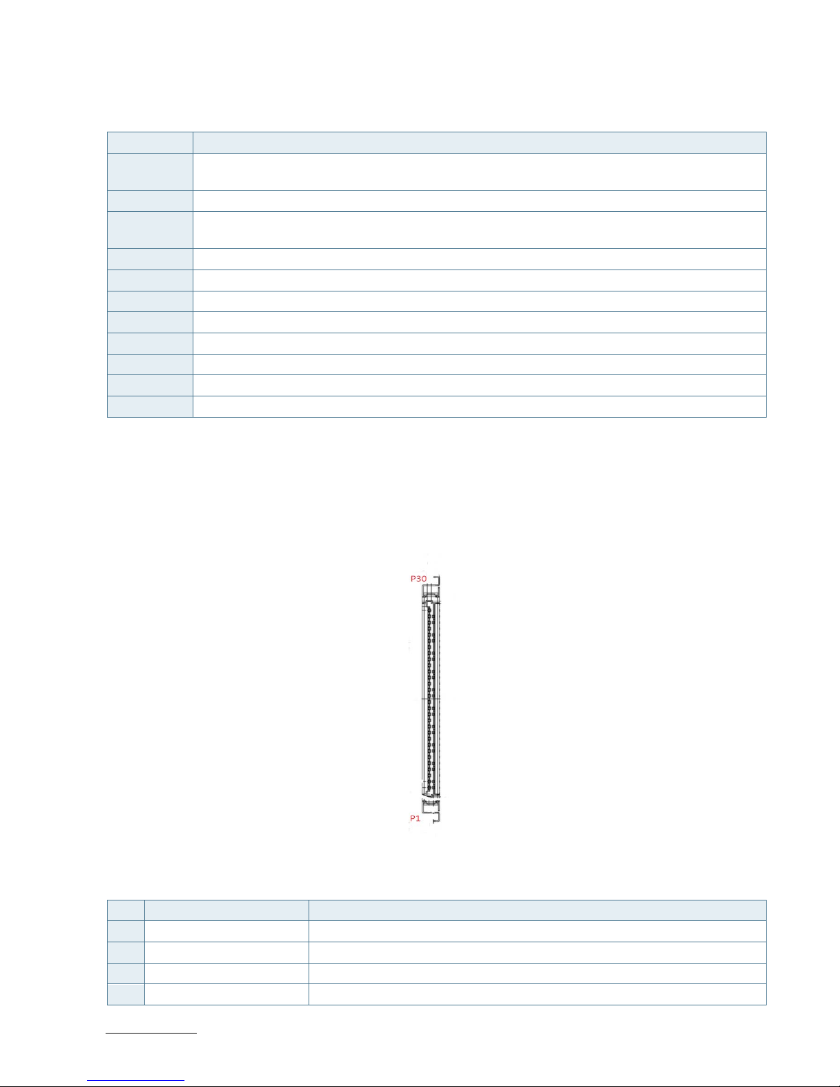
ECX-BYT - User Guide, Rev. 1.0
www.kontron.com
// 42
Table 36: Signal Description
Signal Description
TXD Transmitted Data, sends data to the communications link. The signal is set to the marking state (-12
V) on hardware reset when the transmitter is empty or when loop mode operation is initiated.
RXD Received Data, receives data from the communications link.
DTR Data Terminal Ready, indicates to the modem etc. that the on-board UART is ready to establish
communication link.
DSR Data Set Ready, indicates that the modem etc. is ready to establish a communications link.
RTS Request To Send, indicates to the modem etc. that the on-board UART is ready to exchange data.
CTS Clear To Send, indicates that the modem or data set is ready to exchange data.
DCD Data Carrier Detect, indicates that the modem or data set has detected the data carrier.
RI Ring Indicator, indicates that the modem has received a ringing signal from the telephone line.
TX+/- Transmitted Data differential pair sends data to the communications link.
RX+/- Received Data differential pair receives data from the communications link.
GND Power Supply GND signal
7.10. LVDS Flat Panel Connector (LVDS1)
The LVDS connector is based on 30-pole connector type JAE JS-1267-30(G1)NH.
Figure 24: LVDS Connector LVDS1
Table 37: Pin Assignment LVDS1
Pin Signal Note
1 LVDS_A0-
2 LVDS_A0+
3 LVDS_A1-
4 LVDS_A1+
Page 43

ECX-BYT - User Guide, Rev. 1.0
www.kontron.com
// 43
Pin Signal Note
5 LVDS_A2-
6 LVDS_A2+
7 GND
8 LVDS_ACLK-
9 LVDS_ACLK+
10 LVDS_A3-/NC
11 LVDS_A3+/NC
12 LVDS_B0-
13 LVDS_B0+
14 GND
15 LVDS_B1-
16 LVDS_B1+
17 GND
18 LVDS_B2-
19 LVDS_B2+
20 LVDS_BCLK-
21 LVDS_BCLK+
22 LVDS_B3-/NC
23 LVDS_B3+/NC
24 GND
25 DDC_DATA
26 VDDEN
27 DDC_CLK
28 +3.3V / +5V *
29 +3.3V / +5V*
30 +3.3V / +5V*
* Panel Power can be selected by JP5.
Table 38: Signal Description
Signal Description
LVDS_A0..A3 LVDS A Channel data
LVDS_ACLK LVDS A Channel clock
LVDS_B0..B3 LVDS B Channel data
LVDS_BCLK LVDS B Channel clock
VDDEN Output Display Enable
DDC_DATA DDC channel Data
DDC_CLK DDC Channel Clock
Page 44

ECX-BYT - User Guide, Rev. 1.0
www.kontron.com
// 44
7.11. Backlight Power Output Wafer (CN14)
Figure 25: Backlight Power Output Wafer CN14
Table 39: Pin Assignment CN16
Pin Signal Note
1 BL_ADJ_PWM*
2 BL_ADJ_VOL*
3 GND
4 +5V / +12V**
5 +5V / +12V**
6 GND
7 BL_EN***
* BL_ADJ can be setting in BIOS setup.
** Backlight Power can be selected by JP5.
*** BL_EN can be selected by JP4.
Table 40: Signal Description
Signal Description
BL_ADJ_PWM Backlight Adjustment PWM (Pulse Width Modulation) signal
BL_ ADJ_VOL Backlight Adjustment Voltage signal
BL_EN Backlight Enable signal
Page 45
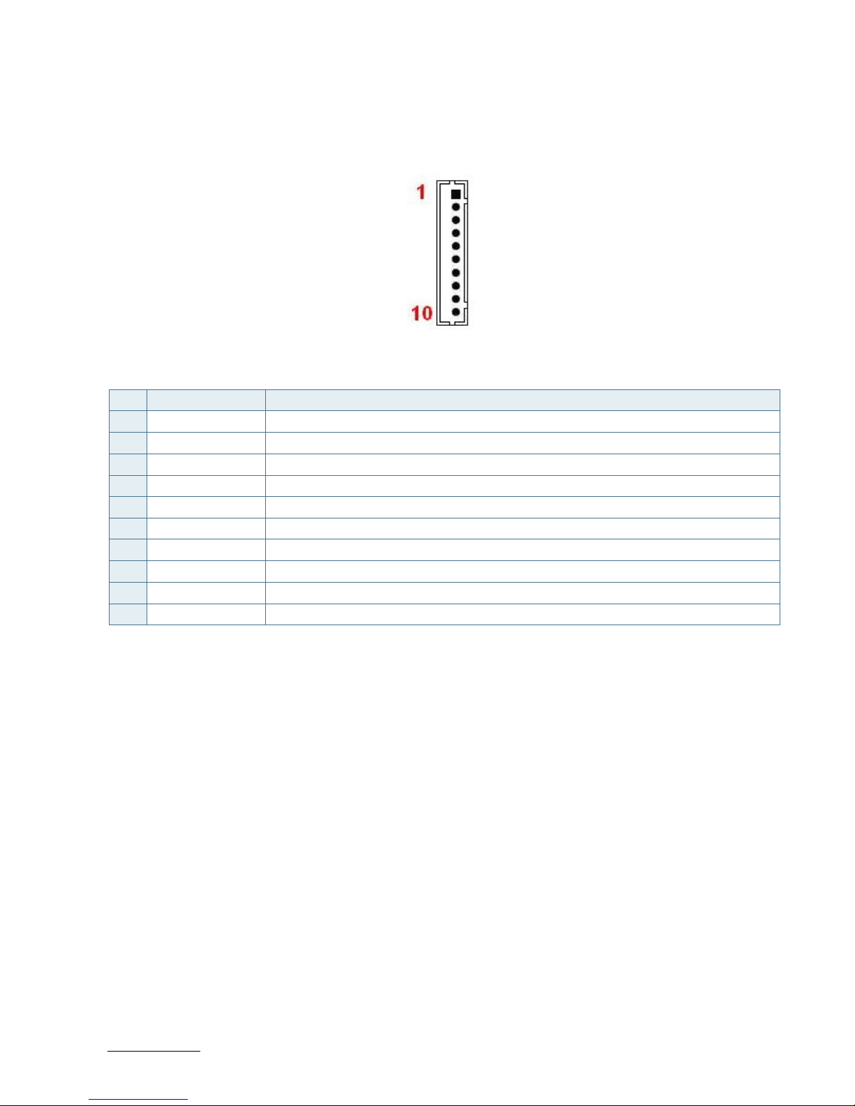
ECX-BYT - User Guide, Rev. 1.0
www.kontron.com
// 45
7.12. Digital Input / Output Wafer (CN13)
Figure 26: Digital Input / Output Wafer CN5
Table 41: Pin Assignment FP2
Pin Signal Note
1 +5V
2 DIO_0
3 DIO_1
4 DIO_2
5 DIO_3
6 DIO_4
7 DIO_5
8 DIO_6
9 DIO_7
10 GND
Page 46
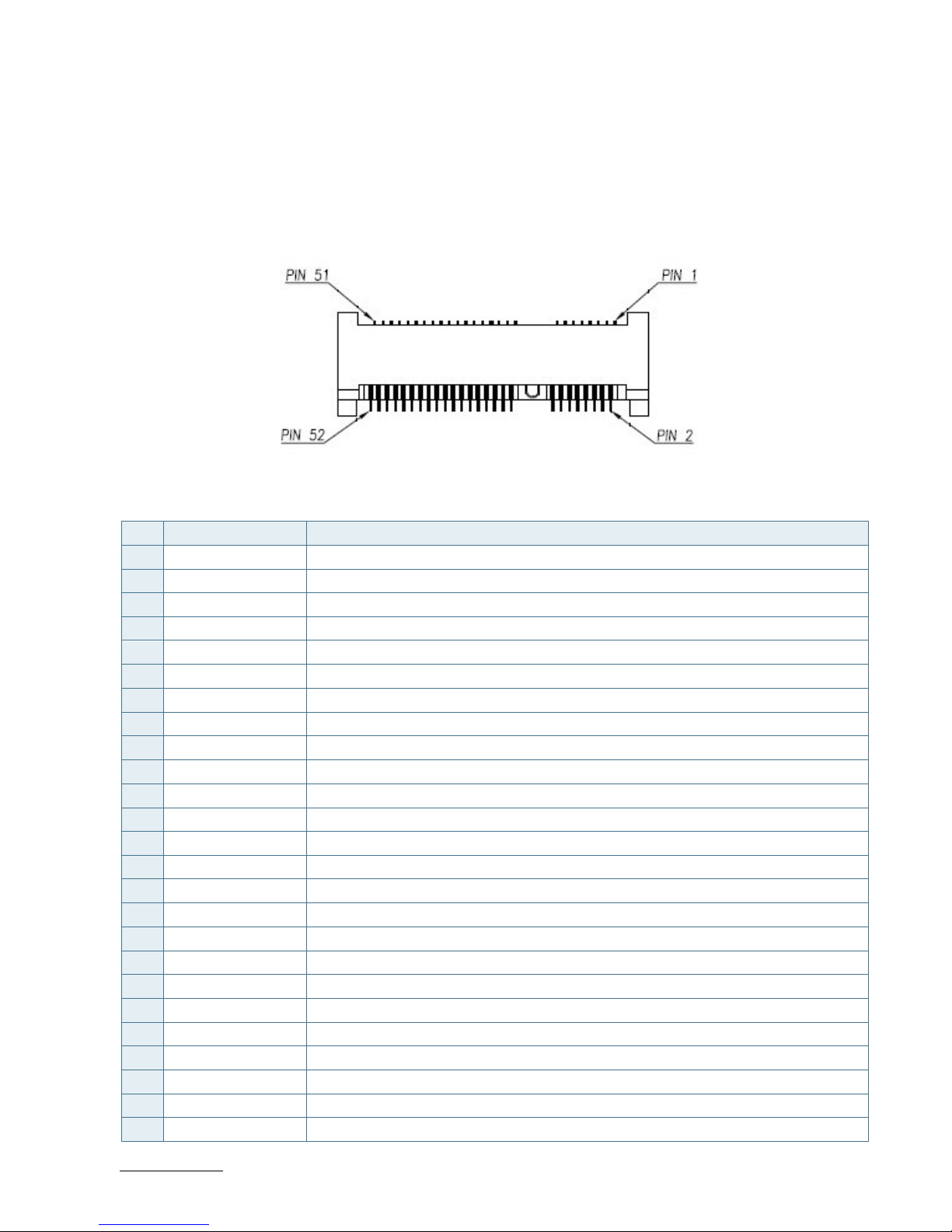
ECX-BYT - User Guide, Rev. 1.0
www.kontron.com
// 46
7.13. mPCIe Slot Connector (MPCIE1)
Full-sized Mini-PCI Express V1.2 socket (MPCIE1). Socket MPCIE1 supports mPCIe, USB2.0 and SIM-card socket. The
SIM-card socket makes it possible to use a 3G/4G-wireless modem in this mPCIe slot. The USB does support WAKE
function.
Figure 27: mPCIe Slot Connector MPCIE1
Table 42: Pin Assignment MPCIE1
Pin Signal Note
1 WAKE#
2 +3.3VSB
3 Reserved
4 Ground
5 Reserved
6 +1.5V
7 CLKREQ#
8 UIM_PWR*
9 Ground
10 UIM_DATA*
11 REFCLK-
12 UIM_CLK*
13 REFCLK+
14 UIM_RESET*
15 Ground
16 UIM_VPP*
17 Reserved
18 Ground
19 Reserved
20 W_Disable#
21 Ground
22 PERST#
23 PERn0
24 +3.3VSB
25 PERp0
Page 47

ECX-BYT - User Guide, Rev. 1.0
www.kontron.com
// 47
Pin Signal Note
26 Ground
27 Ground
28 +1.5V
29 Ground
30 SMB_CLK
31 PETn0
32 SMB_DATA
33 PETp0
34 Ground
35 Ground
36 USB_D-
37 Ground
38 USB_D+
39 +3.3VSB
40 Ground
41 +3.3VSB
42 LED_WWAN#
43 Ground
44 LED_WLAN#
45 Reserved
46 LED_WPAN#
47 Reserved
48 +1.5V
49 Reserved
50 Ground
51 Reserved
52 +3.3VSB
* These pins are connected to CN10 SIM Interface directly.
Page 48

ECX-BYT - User Guide, Rev. 1.0
www.kontron.com
// 48
7.14. SIM Interface Wafer for MPCIE1 (CN10)
Figure 28: SIM Interface Wafer CN10
Table 43: Pin Assignment CN10
Pin Signal Description Note
1 UIM_PWR Power +5V or +3.3V
2 UIM_DATA Input or Output for serial data
3 UIM_RESET Reset signal
4 UIM_VPP Programming voltage input (optional)
5 UIM_CLK Clock signal
6 GND Ground
Page 49

ECX-BYT - User Guide, Rev. 1.0
www.kontron.com
// 49
7.15. mSATA Socket (MSATA1)
Full-sized mSATA socket (MSATA1). The mSATA interface complies with SATA 2.0.
Figure 29: Serial ATA Port-1 mSATA Socket MSATA1
Table 44: Pin Assignment MSATA1
Pin Signal Note
1 NC
2 +3.3V
3 NC
4 Ground
5 NC
6 NC
7 N/A
8 NC
9 Ground
10 NC
11 NC
12 NC
13 NC
14 NC
15 Ground
16 NC
17 NC
18 Ground
19 NC
20 NC
21 Ground
22 NC
23 SATA_RX+
24 +3.3V
25 SATA_RX-
26 Ground
Page 50

ECX-BYT - User Guide, Rev. 1.0
www.kontron.com
// 50
Pin Signal Note
27 Ground
28 NC
29 Ground
30 NC
31 SATA_TX-
32 NC
33 SATA_TX+
34 Ground
35 Ground
36 NC
37 Ground
38 NC
39 +3.3V
40 Ground
41 +3.3V
42 NC
43 Ground
44 NC
45 NC
46 NC
47 NC
48 NC
49 NC
50 Ground
51 NC
52 +3.3V
Page 51

ECX-BYT - User Guide, Rev. 1.0
www.kontron.com
// 51
7.16. PS/2 Keyboard and Mouse Wafer (CN2)
The audio connector provides audio output (Line-Out), audio input (Line-In) and microphone (Mic-In) signals through
the wafer CN9. The audio output signals are shared with those of the speaker connectors CN11 & CN12.
Figure 30: PS/2 Keyboard / Mouse Wafer CN2
Table 45: Pin Assignment CN2
Pin Signal Note
1 MSCLK
2 VCC
3 MSDAT
4 KBDAT
5 GND
6 KBCLK
Table 46: Signal Description
Signal Description
MSCLK Bi-directional clock signal used to strobe data/commands from/to the PS/2 mouse.
MSDAT Bi-directional serial data line used to transfer data from or commands to the PS/2 mouse.
KBCLK Bi-directional clock signal used to strobe data/commands from/to the PC-AT keyboard.
KBDAT Bi-directional serial data line used to transfer data from or commands to the PC-AT keyboard.
Page 52

ECX-BYT - User Guide, Rev. 1.0
www.kontron.com
// 52
7.17. Switches and Jumpers
The product has several jumpers which must be properly configured to ensure correct operation.
Figure 31: Jumper Connector
For a three-pin jumper (see Figure 35), the jumper setting is designated “1-2” when the jumper connects pins 1 and 2.
The jumper setting is designated “2-3” when pins 2 and 3 are connected and so on. You will see that one of the lines
surrounding a jumper pin is thick, which indicates pin No.1.
To move a jumper from one position to another, use needle-nose pliers or tweezers to pull the pin cap off the pins
and move it to the desired position.
7.17.1. RTC Reset Selection (JP1)
The "RTC Reset" jumper (JP1) can be used to reset the Real Time Clock (RTC) and drain RTC well.
The jumper has one position: Pin 1-2 and not mounted (default position). More information on setting the "RTC Reset"
jumper can be founf in the following table.
Figure 32: RTC Reset Selection (JP1)
Table 47: Pin Assignment JP1
Jumper Position
Description
Pin 1-2
X Enable Clear CMOS RTC content
(board does not boot with the jumper in this position)
- Normal operation (default position)
“X” = Jumper set (short) and “-” = jumper not set (open)
Do not leave the jumper in position 1-2, otherwise if the power is disconnected, the
battery will fully deplete within a few weeks.
Page 53
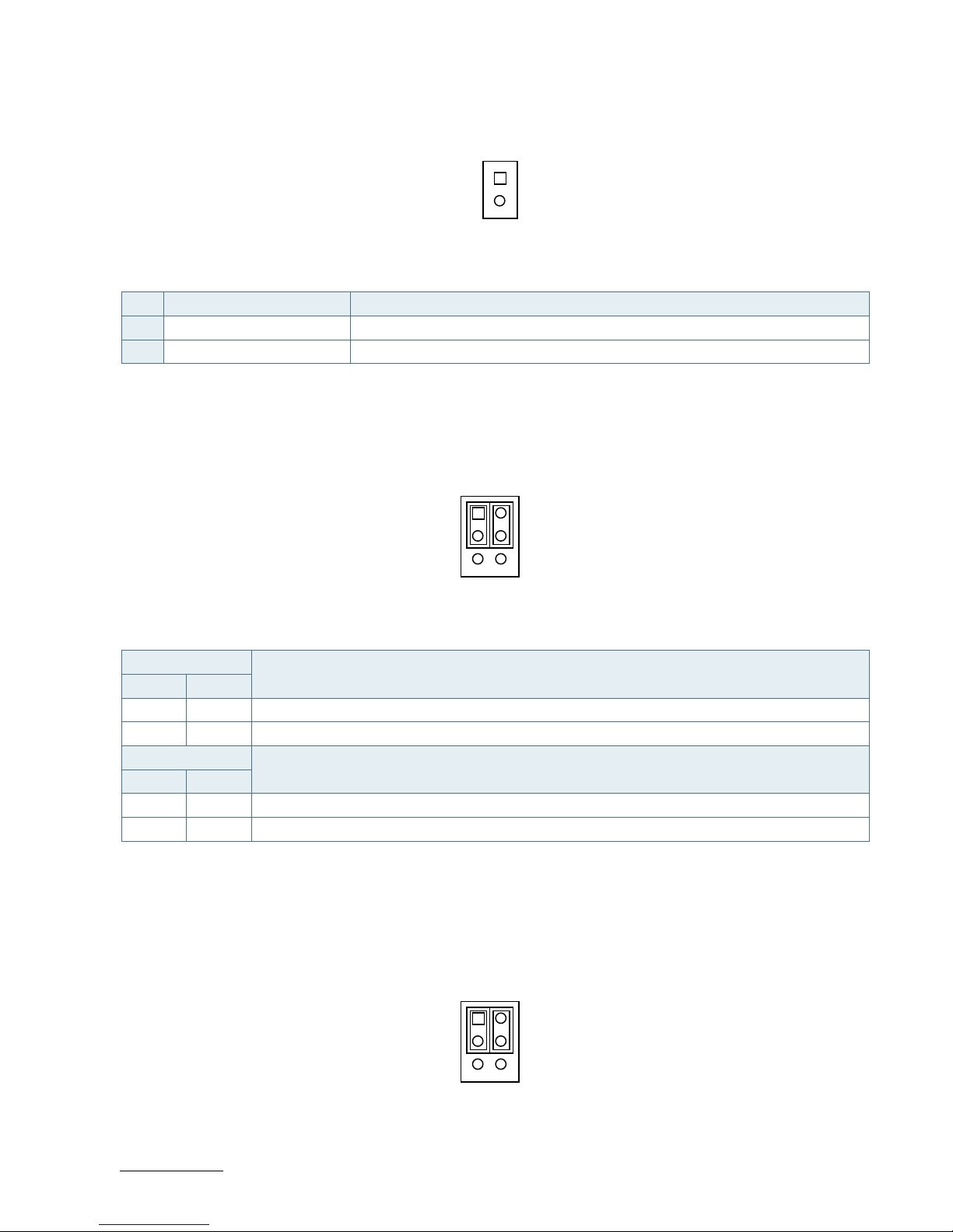
ECX-BYT - User Guide, Rev. 1.0
www.kontron.com
// 53
7.17.2. MPCIE1 Activity LED Indication (JP2)
Figure 33: MPCIE1 Activity LED Indication JP2
Table 48: Pin Assignment JP2
Pin Signal Note
1 LED+
2 LED-
7.17.3. Backlight Enable Selection for LVDS1 (JP4)
Figure 34: Backlight Enable Selection JP4
Table 49: Pin Assignment JP4
Jumper 1 Position
Description
Pin 1-3 Pin 3-5
X - Backlight Enable Voltage = +3.3V
- X Backlight Enable Voltage = +5V
Jumper 2 Position
Description
Pin 2-4 Pin 4-6
X - Active High
- X Active Low
“X” = Jumper set (short) and “-” = jumper not set (open)
7.17.4. Panel & Backlight Power Selection for LVDS1 (JP5)
Figure 35: Panel & Backlight Power Selection JP5
1
2
21
65
21
65
Page 54

ECX-BYT - User Guide, Rev. 1.0
www.kontron.com
// 54
Table 50: Pin Assignment JP5
Jumper 1 Position
Description
Pin 1-3 Pin 3-5
X - Backlight Power = +12V
- X Backlight Power = +5V
Jumper 2 Position
Description
Pin 2-4 Pin 4-6
X - Panel Power = +3,3V
- X Panel Power = +5V
“X” = Jumper set (short) and “-” = jumper not set (open)
7.17.5. USB Power Selection (JP6)
Figure 36: USB Power Selection JP6
Table 51: Pin Assignment JP6
Jumper Position
Description
Pin 1-2
X USB power is always supply.
- USB power will be cut off in S4 & S5 state.
“X” = Jumper set (short) and “-” = jumper not set (open)
7.17.6. AT / ATX Power Mode Selection (JP7)
Figure 37: AT / ATX Power Mode Selection JP7
Table 52: Pin Assignment JP7
Jumper 1 Position
Description
Pin 1-2 Pin 2-3
X - ATX Mode
- X AT Mode
“X” = Jumper set (short) and “-” = jumper not set (open)
2
3
1
Page 55

ECX-BYT - User Guide, Rev. 1.0
www.kontron.com
// 55
7.17.7. ME F/W Selection (JP8)
Figure 38: ME F/W Selection JP8
Table 53: Pin Assignment JP8
Jumper Position
Description
Pin 1-2
X ME F/W Disabled
- Normal Operation
“X” = Jumper set (short) and “-” = jumper not set (open)
Page 56

ECX-BYT - User Guide, Rev. 1.0
www.kontron.com
// 56
8/ On-Board Connectors & Mating Connector Types
The Mating connectors / Cables are connectors or cable kits which are fitting the On-board connector.
The cable kits marked with "*" are included in the "ECX-BYT Cable & Driver Kit".
Table 54: On-Board Connectors & Mating Connector Types
Connector On-Board Connectors Mating Connectors / Cables
Manufact. Type No. Manufact. Type No.
Battery Input (BAT1) Pinrex 712-73-02TWR0
COM (COM1 ~ COM6) Pinrex 712-73-10TWB0 0C5020000000910L
DC 12V Power Input (CN1) Pinrex 733-97-04TBR1 0C5020000001580L
Keyboard/Mouse (CN2) YIMTEX 503PW1*06ST-1R 0C5020002500010L
HDD Power Output (CN3) Pinrex 721-93-04TWE9 0C5020000001590L
Audio Input / Output (CN9) Pinrex 212-92-06GBE1 0C5020000002050L
SIM (CN10) Pinrex 712-73-06TWB0 0ZHK12003GSIM003
Audio AMP (CN11, CN12) YIMTEX 503PW1*02STR &
503PW1*02ST-1R
DIO (CN13) Pinrex 712-73-10TWB0 0C5020000002060L
Backlight Power (CN16) Townes
Enterprise
1250W-07T1-V
FAN (FAN1) Pinrex 712-73-03TWE0
Front Panel (FP1) YIMTEX 3362*04SANGR
Front Panel (FP2) YIMTEX 3362*05SANGR
LVDS Panel (LVDS1) JAE JS-1267-30(G1)NH
mPCIe (MPCIE1) FOXCONN AS0B226-S99Q-7H
mSATA (MSATA1) LOTES AAA-PCI-093-K01
SATA (SATA1) FOXCONN LD1807V-S52U 0C5020000004240L
USB 2.0 (CN15) Pinrex 712-73-04TWE0 0C5020000003220L
USB 2.0 (CN16) YIMTEX 3362*05SANGR-09 0C502USB0201010L
Please note that standard connectors like DP, mPCIe, Audio Jack, Ethernet and USB are
not included in the list.
Page 57

ECX-BYT - User Guide, Rev. 1.0
www.kontron.com
// 57
9/ BIOS
9.1. Starting the uEFI BIOS
The ECX-BYT is provided with a Kontron-customized, pre-installed and configured version of AMI Aptio® V uEFI BIOS.
AMI BIOS firmware is based on the Unified Extensible Firmware Interface (UEFI) specification and the Intel® Platform
Innovation Framework for EFI. This uEFI BIOS provides a variety of new and enhanced functions specifically tailored to
the hardware features of the ECX-BYT.
The uEFI BIOS comes with a setup program that provides quick and easy access to the individual function settings for
control or modification of the uEFI BIOS configuration. The setup program allows the accessing of various menus that
provide functions or access to sub-menus with more specific functions of their own.
To start the uEFI BIOS setup program, follow the steps below:
1. Power on the board.
2. Wait until the first characters appear on the screen (POST messages or splash screen).
3. Press the <DEL> key.
4. If the uEFI BIOS is password-protected, a request for password will appear. Enter either the User Password or the
Supervisor Password (see Security menu), press <RETURN>, and proceed with step 5.
5. A setup menu will appear.
The ECX-BYT uEFI BIOS setup program uses a hot key-based navigation system. A hot key legend bar is located on the
bottom of the setup screens.
The following table provides information concerning the usage of these hot keys.
Table 55: Font Size Table
Hotkeys Description
<F1> The <F1> key invokes the General Help window.
<-> The <Minus> key selects the next lower value within a field.
<+> The <Plus> key selects the next higher value within a field.
<F2> The <F2> key loads the previous values.
<F3> The <F3> key loads the standard default values.
<F4> The <F4> key saves the current settings and exit the uEFI BIOS setup.
<→> or <←>
The <Left/Right> arrows selects major setup menus on the menu bar. For example:
Main, Advanced, Security, etc.
<↑> or <↓>
The <Up/Down> arrows selects fields in the current menu. For example: A setup
function or a sub-screen.
<ESC> The <ESC> key exits a major setup menu and enter the Exit setup menu.
Pressing the <ESC> key in a sub-menu displays the next higher menu level.
<RERURN> The <RETURN> key executes a command or select a submenu.
Page 58

ECX-BYT - User Guide, Rev. 1.0
www.kontron.com
// 58
9.2. Setup Menus
The Setup utility features shows six menus in the selection bar at the top of the screen:
Main
Advanced
Power
Boot
Security
Save & Exit
The Setup menus are selected via the left and right arrow keys. The currently active menu and the currently active
uEFI BIOS Setup item are highlighted in white. Each Setup menu provides two main frames. The left frame displays all
available functions. Functions that can be configured are displayed in blue. Functions displayed in gray provide
information about the status or the operational configuration. The right frame displays an Item Specific Help window
providing an explanation of the respective function.
9.2.1. Main Setup Menu
Upon entering the uEFI BIOS Setup program, the Main Setup menu is displayed. This screen lists the Main Setup menu
sub-screens and provides basic system information. Additionally functions for setting the system time and date are
offered.
Table 56: Main Setup Menu Sub-Screens and Functions
Function Description
BIOS Information Read only field.
Displays information about the system BIOS
Memory Information Read only field.
Displays information about total memory
ME Information Read only field.
Displays information about Intel Management Engine (ME) version
TXE Information Read only field.
Displays information about TXE information
Firmware Information Code version and firmware information
System Date Set System Date
System Time Set System Time
Page 59

ECX-BYT - User Guide, Rev. 1.0
www.kontron.com
// 59
Figure 39: BIOS Main Menu Screen System Data and Time
BIOS SETUP UTILITY
Main Advanced Power Boot Security Save & Exit
Product Information
Product Name ECX-BYT-J1900
BIOS Version R0.0A (x64)
BIOS Build Date 05/26/2014
ME FW Version 01.01.00.1089
CPU Information
Intel® Celeron® CPU J1900 @ 1.99GHz
Microcode Revision 809
Processor Cores 2
→ ←: Select Screen
Memory Information
↑ ↓: Select Item
Total Size 4069 MB (DDR3L) Enter: Select
Frequency 1333 MHz +/-: Change Opt.
F1: General Help
System Date [Mon 05/26/2014] F2: Previous Values
System Time [13:23:12] F3: Optimized Defaults
F4: Save & Exit
Access Level Administrator ESC: Exit
Version 2.16.1242. Copyright (C) 2013, American Megatrends, Inc.
Feature Option Description
System Date [dd/mm/yyyy] Set the Date. Use Tab to switch between Data elements.
System Time [hh:mm:ss] Set the Time. Use Tab to switch between Time elements.
Page 60

ECX-BYT - User Guide, Rev. 1.0
www.kontron.com
// 60
9.2.2. Advanced Setup Menu
The Advanced setup menu provides sub-screens and functions for advanced configurations. The following subscreen functions are included in the menu:
LAN & Audio Configuration
Display Configuration
Super IO Configuration
CPU Chipset Configuration
SATA Configuration
USB Configuration
DIO Configuration
H/W Monitor
Setting items on this screen to incorrect values may cause the system to malfunction.
Page 61
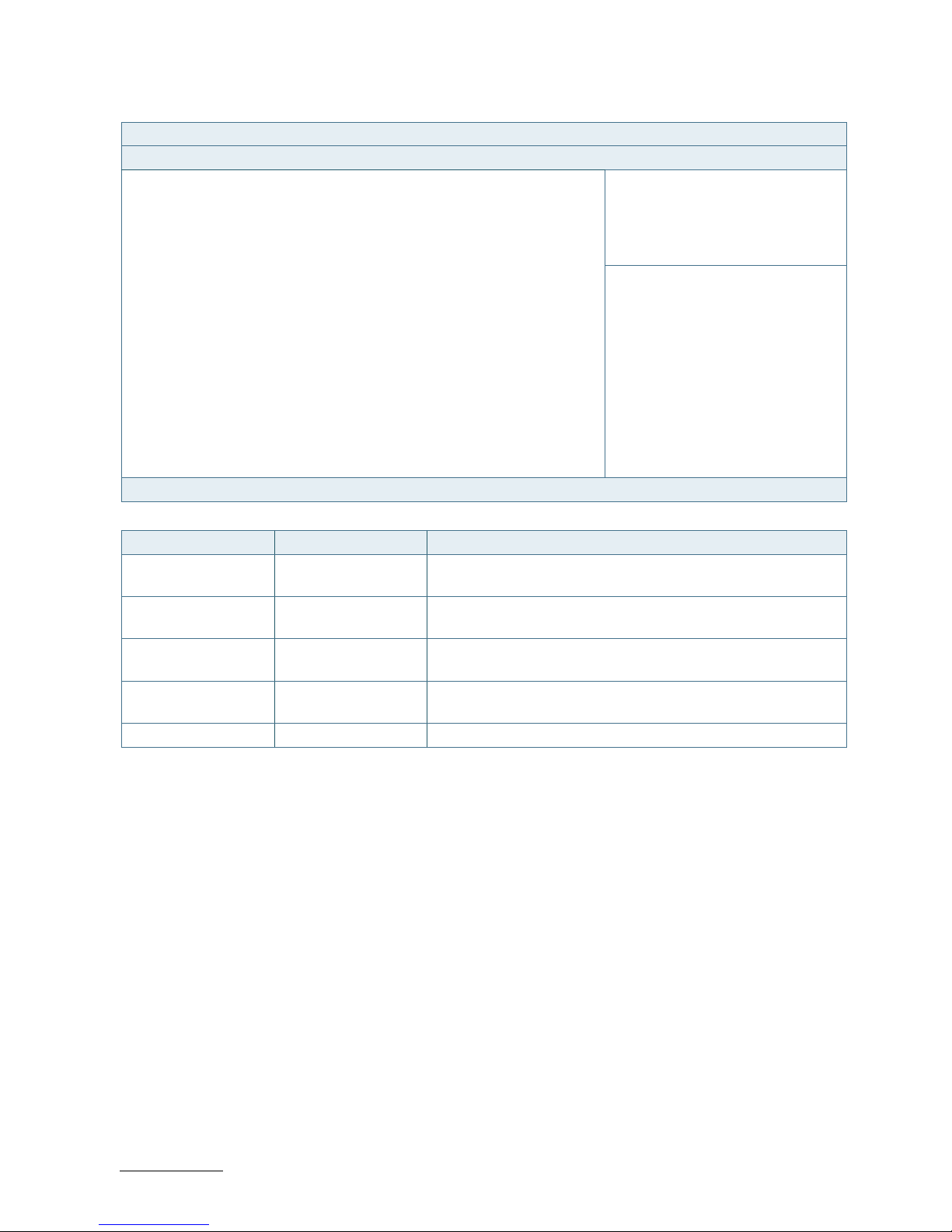
ECX-BYT - User Guide, Rev. 1.0
www.kontron.com
// 61
Figure 40: BIOS Advanced Menu
BIOS SETUP UTILITY
Main Advanced Power Boot Security Save & Exit
Onboard LAN1 Controller [Enabled]
Onboard LAN1 Boot [Disabled]
Onboard LAN2 Controller [Enabled]
Onboard LAN2 Boot [Disabled]
Audio Controller [Enabled]
→ ←: Select Screen
↑ ↓: Select Item
> Display Configuration Enter: Select
> Super IO Configuration +/-: Change Opt.
> CPU Chipset Configuration F1: General Help
> SATA Configuration F2: Previous Values
> USB Configuration F3: Optimized Defaults
> DIO Configuration F4: Save & Exit
> H/W Monitor ESC: Exit
Version 2.16.1242. Copyright (C) 2013, American Megatrends, Inc.
Feature Option Description
Onboard LAN1
Controller
[Disabled], [Enabled] Select whether to enable or disable Onboard LAN1 Controller.
Onboard LAN1 Boot [Disabled], [Enabled] Select whether to enable or disable load onboard PXE (Preboot
Execution Environment).
Onboard LAN2
Controller
[Disabled], [Enabled] Select whether to enable or disable Onboard LAN2 Controller.
Onboard LAN2 Boot [Disabled], [Enabled] Select whether to enable or disable load onboard PXE (Preboot
Execution Environment).
Audio Controller [Disabled], [Enabled] Select whether to enable or disable Audio Controller.
Page 62

ECX-BYT - User Guide, Rev. 1.0
www.kontron.com
// 62
Figure 41: BIOS Advanced Menu - Display Configuration
BIOS SETUP UTILITY
Main Advanced Power Boot Security Save & Exit
Display Configuration
Primary Display [Auto]
UWA Frame Buffer Size [256MB]
→ ←: Select Screen
DVMT Pre-Allocated [64M]
↑ ↓: Select Item
DVMT Total Gfx Mem [256M] Enter: Select
+/-: Change Opt.
Primary IGFX Boot Display [VBIOS Default] F1: General Help
Active LVDS [Disabled] F2: Previous Values
LVDS Panel Type* [1024x768 18Bit 1CH] F3: Optimized Defaults
LVDS Backlight Control Mode* [PWM] F4: Save & Exit
LVDS Backlight Control - Voltage* [3.5V] ESC: Exit
Version 2.16.1242. Copyright (C) 2013, American Megatrends, Inc.
* These items appear only when enbling Active LVDS.
Feature Option Description
Primary Display [Auto], [IGD] Select which graphic controller to be used as the primary
display device.
UWA Frame Buffer
Size
[128MB], [256MB],
[512MB]
Select the Aperture Size.
DVMT Pre-Allocated [64M], [96M], [128M],
[160M], [192M],
[224M], [256M],
[288M], [320M],
[352M], [384M],
[416M], [448M],
[480M], [512M]
Select DVMT Pre-Allocated (Fixed) Graphics Memory size used
by the Internal Graphics Device.
DVMT Total Gfx Mem [128M], [256M], [MAX] Select DVMT Total Graphic Memory size used by the Internal
Graphics Device.
Primary IGFX Boot
Display
[VBIOS Default],
[CRT], [HDMI], [LVDS]
Select the Video Device which will be activated during POST. This
has no effect if external graphics present.
Secondary boot display selection will appear based on your
selection.
DOS modes will be supported only on primary display.
Active LVDS [Disabled], [Enabled] Select the Active LVDS Configuration.
[Disabled]: VBIOS does not enable LVDS.
[Enabled]: VBIOS will enable LVDS.
LVDS Panel Type [640x480 18Bit 1CH],
[800x480 18Bit 1CH],
[800x600 18Bit 1CH],
[1024x768 18Bit 1CH],
[1440x900 18Bit 1CH],
[1600x900 18Bit 1CH]
Select the appropriate setup item for LVDS panel.
LVDS Backlight [Voltage], [PWM] Select the appropriate setup item for LVDS backlight control
Page 63

ECX-BYT - User Guide, Rev. 1.0
www.kontron.com
// 63
Feature Option Description
Control Mode mode.
LVDS Backlight
Control - Voltage
[0.0V], [0.5V], [1.0V],
[1.5V], [2.0V], [3.0V],
[3.5V], [4.0V], [4.5V],
[5.0V]
Select the voltage of LVDS backlight control mode.
Page 64

ECX-BYT - User Guide, Rev. 1.0
www.kontron.com
// 64
Figure 42: BIOS Advanced Menu - Super IO Configuration
BIOS SETUP UTILITY
Main Advanced Power Boot Security Save & Exit
Super IO Configuration
> Serial Port 1 Configuration
→ ←: Select Screen
> Serial Port 2 Configuration
↑ ↓: Select Item
> Serial Port 3 Configuration Enter: Select
> Serial Port 4 Configuration +/-: Change Opt.
> Serial Port 5 Configuration F1: General Help
> Serial Port 6 Configuration F2: Previous Values
F3: Optimized Defaults
F4: Save & Exit
ESC: Exit
Version 2.16.1242. Copyright (C) 2013, American Megatrends, Inc.
Figure 43: BIOS Advanced Menu - Super IO Configuration - Serial Port 1 Configuration
BIOS SETUP UTILITY
Main Advanced Power Boot Security Save & Exit
Serial Port 1 Configuration
Serial Port [Enabled]
→ ←: Select Screen
Device Settings IO=3F8h; IRQ=4;
↑ ↓: Select Item
Enter: Select
Change Setting [Auto] +/-: Change Opt.
Serial Port 1 Type [RS232] F1: General Help
RS485 Deplux Mode* [Half Duplex] F2: Previous Values
F3: Optimized Defaults
F4: Save & Exit
ESC: Exit
Version 2.16.1242. Copyright (C) 2013, American Megatrends, Inc.
* These items appear only when selecting RS485 for the Serial Port 1 Type.
Feature Option Description
Serial Port [Disabled], [Enabled] Select whether to enable or disable Serial Port (COM).
Change Settings [Auto], [IO=3F8h;
IRQ=4;], [IO=3F8h;
IRQ=3, 4, 5, 6, 7, 9, 10,
11, 12;], [IO=2F8h;
IRQ=3, 4, 5, 6, 7, 9, 10,
11, 12;], [IO=3E8h;
IRQ=3, 4, 5, 6, 7, 9, 10,
11, 12;], [IO=2E8h;
IRQ=3, 4, 5, 6, 7, 9, 10,
11, 12;]
Select an optional setting for Super IO device.
Page 65
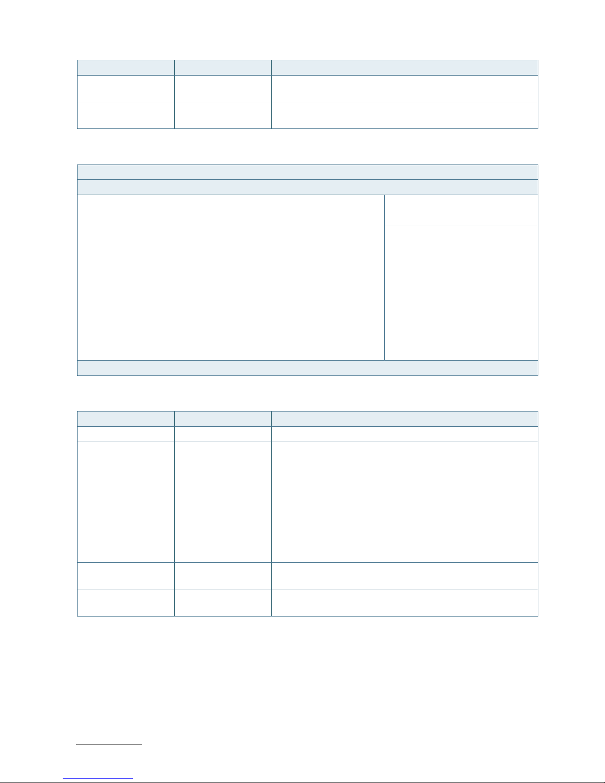
ECX-BYT - User Guide, Rev. 1.0
www.kontron.com
// 65
Feature Option Description
Serial Port 1 Type [RS232], [RS422],
[RS485]
Select an appropriate type for Serial Port 1.
RS485 Duplex Mode [Half Duplex], [Full
Duplex]
Select an appropriate RS485 Duplex Mode.
Figure 44: BIOS Advanced Menu - Super IO Configuration - Serial Port 2 Configuration
BIOS SETUP UTILITY
Main Advanced Power Boot Security Save & Exit
Serial Port 2 Configuration
Serial Port [Enabled]
→ ←: Select Screen
Device Settings IO=2F8h; IRQ=3;
↑ ↓: Select Item
Enter: Select
Change Setting [Auto] +/-: Change Opt.
Serial Port 2 Type [RS232] F1: General Help
RS485 Deplux Mode* [Half Duplex] F2: Previous Values
F3: Optimized Defaults
F4: Save & Exit
ESC: Exit
Version 2.16.1242. Copyright (C) 2013, American Megatrends, Inc.
* These items appear only when selecting RS485 for the Serial Port 2 Type.
Feature Option Description
Serial Port [Disabled], [Enabled] Select whether to enable or disable Serial Port (COM).
Change Settings [Auto], [IO=2F8h;
IRQ=3;], [IO=3F8h;
IRQ=3, 4, 5, 6, 7, 9, 10,
11, 12;], [IO=2F8h;
IRQ=3, 4, 5, 6, 7, 9, 10,
11, 12;], [IO=3E8h;
IRQ=3, 4, 5, 6, 7, 9, 10,
11, 12;], [IO=2E8h;
IRQ=3, 4, 5, 6, 7, 9, 10,
11, 12;]
Select an optional setting for Super IO device.
Serial Port 2 Type [RS232], [RS422],
[RS485]
Select an appropriate type for Serial Port 2.
RS485 Duplex Mode [Half Duplex], [Full
Duplex]
Select an appropriate RS485 Duplex Mode.
Page 66

ECX-BYT - User Guide, Rev. 1.0
www.kontron.com
// 66
Figure 45: BIOS Advanced Menu - Super IO Configuration - Serial Port 3 Configuration
BIOS SETUP UTILITY
Main Advanced Power Boot Security Save & Exit
Serial Port 3 Configuration
Serial Port [Enabled]
→ ←: Select Screen
Device Settings IO=3E8h; IRQ=7;
↑ ↓: Select Item
Enter: Select
Change Setting [Auto] +/-: Change Opt.
F1: General Help
F2: Previous Values
F3: Optimized Defaults
F4: Save & Exit
ESC: Exit
Version 2.16.1242. Copyright (C) 2013, American Megatrends, Inc.
Feature Option Description
Serial Port [Disabled], [Enabled] Select whether to enable or disable Serial Port (COM).
Change Settings [Auto], [IO=3E8h;
IRQ=7;], [IO=3E8h;
IRQ=3, 4, 5, 6, 7, 9, 10,
11, 12;], [IO=2E8h;
IRQ=3, 4, 5, 6, 7, 9, 10,
11, 12;], [IO=2F0h;
IRQ=3, 4, 5, 6, 7, 9, 10,
11, 12;], [IO=2E0h;
IRQ=3, 4, 5, 6, 7, 9, 10,
11, 12;]
Select an optional setting for Super IO device.
Figure 46: BIOS Advanced Menu - Super IO Configuration - Serial Port 4 Configuration
BIOS SETUP UTILITY
Main Advanced Power Boot Security Save & Exit
Serial Port 4 Configuration
Serial Port [Enabled]
→ ←: Select Screen
Device Settings IO=2E8h; IRQ=7;
↑ ↓: Select Item
Enter: Select
Change Setting [Auto] +/-: Change Opt.
F1: General Help
F2: Previous Values
F3: Optimized Defaults
F4: Save & Exit
ESC: Exit
Version 2.16.1242. Copyright (C) 2013, American Megatrends, Inc.
Page 67

ECX-BYT - User Guide, Rev. 1.0
www.kontron.com
// 67
Feature Option Description
Serial Port [Disabled], [Enabled] Select whether to enable or disable Serial Port (COM).
Change Settings [Auto], [IO=2E8h;
IRQ=7;], [IO=3F8h;
IRQ=3, 4, 5, 6, 7, 9, 10,
11, 12;], [IO=2F8h;
IRQ=3, 4, 5, 6, 7, 9, 10,
11, 12;], [IO=3E8h;
IRQ=3, 4, 5, 6, 7, 9, 10,
11, 12;], [IO=2E8h;
IRQ=3, 4, 5, 6, 7, 9, 10,
11, 12;], [IO=2F0h;
IRQ=3, 4, 5, 6, 7, 9, 10,
11, 12;], [IO=2E0h;
IRQ=3, 4, 5, 6, 7, 9, 10,
11, 12;]
Select an optional setting for Super IO device.
Figure 47: BIOS Advanced Menu - Super IO Configuration - Serial Port 5 Configuration
BIOS SETUP UTILITY
Main Advanced Power Boot Security Save & Exit
Serial Port 5 Configuration
Serial Port [Enabled]
→ ←: Select Screen
Device Settings IO=2F0h; IRQ=7;
↑ ↓: Select Item
Enter: Select
Change Setting [Auto] +/-: Change Opt.
F1: General Help
F2: Previous Values
F3: Optimized Defaults
F4: Save & Exit
ESC: Exit
Version 2.16.1242. Copyright (C) 2013, American Megatrends, Inc.
Feature Option Description
Serial Port [Disabled], [Enabled] Select whether to enable or disable Serial Port (COM).
Change Settings [Auto], [IO=2F0h;
IRQ=7;], [IO=3E8h;
IRQ=3, 4, 5, 6, 7, 9, 10,
11, 12;], [IO=2E8h;
IRQ=3, 4, 5, 6, 7, 9, 10,
11, 12;], [IO=2F0h;
IRQ=3, 4, 5, 6, 7, 9, 10,
11, 12;], [IO=2E0h;
IRQ=3, 4, 5, 6, 7, 9, 10,
11, 12;]
Select an optional setting for Super IO device.
Page 68

ECX-BYT - User Guide, Rev. 1.0
www.kontron.com
// 68
Figure 48: BIOS Advanced Menu - Super IO Configuration - Serial Port 6 Configuration
BIOS SETUP UTILITY
Main Advanced Power Boot Security Save & Exit
Serial Port 6 Configuration
Serial Port [Enabled]
→ ←: Select Screen
Device Settings IO=2E0h; IRQ=7;
↑ ↓: Select Item
Enter: Select
Change Setting [Auto] +/-: Change Opt.
F1: General Help
F2: Previous Values
F3: Optimized Defaults
F4: Save & Exit
ESC: Exit
Version 2.16.1242. Copyright (C) 2013, American Megatrends, Inc.
Feature Option Description
Serial Port [Disabled], [Enabled] Select whether to enable or disable Serial Port (COM).
Change Settings [Auto], [IO=2E0h;
IRQ=7;], [IO=3E8h;
IRQ=3, 4, 5, 6, 7, 9, 10,
11, 12;], [IO=2E8h;
IRQ=3, 4, 5, 6, 7, 9, 10,
11, 12;], [IO=2F0h;
IRQ=3, 4, 5, 6, 7, 9, 10,
11, 12;], [IO=2E0h;
IRQ=3, 4, 5, 6, 7, 9, 10,
11, 12;]
Select an optional setting for Super IO device.
Page 69

ECX-BYT - User Guide, Rev. 1.0
www.kontron.com
// 69
Figure 49: BIOS Advanced Menu - CPU Chipset Configuration
BIOS SETUP UTILITY
Main Advanced Power Boot Security Save & Exit
CPU Chipset Configuration
EIST [Enabled]
→ ←: Select Screen
Limit CPUID Maximum [Disabled]
↑ ↓: Select Item
Execute Disable Bit [Enabled] Enter: Select
Intel Virtualization Technology [Disabled] +/-: Change Opt.
F1: General Help
F2: Previous Values
F3: Optimized Defaults
F4: Save & Exit
ESC: Exit
Version 2.16.1242. Copyright (C) 2013, American Megatrends, Inc.
Feature Option Description
EIST [Disabled], [Enabled] Select whether to enable or disable Enhanced Intel SpeedStep
Technology.
Limit CPUID Maximum [Disabled], [Enabled] Select whether to limit CPUID maximum value.
Execute Disable Bit [Disabled], [Enabled] Select whether to enable or disable Execute Disable Bit
functionality, which prevents malicious buffer overflow attacks..
Intel Virtualization
Technology
[Disabled], [Enabled] Select whether to enable or disable Intel Virtualization
Technology.
Page 70

ECX-BYT - User Guide, Rev. 1.0
www.kontron.com
// 70
Figure 50: BIOS Advanced Menu - SATA Configuration
BIOS SETUP UTILITY
Main Advanced Power Boot Security Save & Exit
SATA Controller(s)
Serial-ATA (SATA) [Enabled]
→ ←: Select Screen
SATA Mode [AHCI Mode]
↑ ↓: Select Item
Enter: Select
Serial ATA Port 1 Empty +/-: Change Opt.
Port 1 [Enabled] F1: General Help
mS ATA Port 1 Empty F2: Previous Values
Port 1 [Enabled] F3: Optimized Defaults
F4: Save & Exit
ESC: Exit
Version 2.16.1242. Copyright (C) 2013, American Megatrends, Inc.
Feature Option Description
Serial-ATA(SATA) [Enabled], [Disabled] Select whether to enable or disable SATA Device.
SATA Mode [IDE Mode], [AHCI
Mode]
Determine how SATA controller(s) operate.
Port 1 [Disabled], [Enabled] Select whether to enable or disable SATA Port 1 or mSATA Port 1.
Page 71
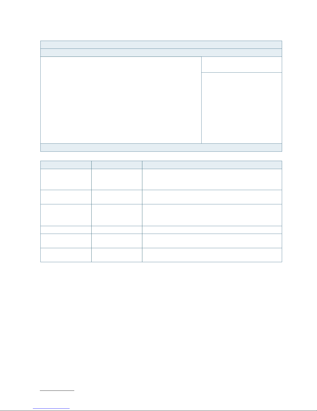
ECX-BYT - User Guide, Rev. 1.0
www.kontron.com
// 71
Figure 51: BIOS Advanced Menu - USB Configuration
BIOS SETUP UTILITY
Main Advanced Power Boot Security Save & Exit
USB Configuration
USB Devices:
→ ←: Select Screen
1 Keyboard, 2 Hubs
↑ ↓: Select Item
Enter: Select
Legacy USB Support [Enabled] +/-: Change Opt.
XHCI Legacy Support [Enabled] F1: General Help
XHCI Hand-off [Enabled] F2: Previous Values
EHCI Hand-off [Disabled] F3: Optimized Defaults
USB Mass Storage Driver Support [Enabled] F4: Save & Exit
XHCI Mode [Smart Auto] ESC: Exit
Version 2.16.1242. Copyright (C) 2013, American Megatrends, Inc.
Feature Option Description
Legacy USB Support [Enabled], [Disabled],
[Auto]
Select whether to enable or disable Legacy USB support.
AUTO option disables legacy support if no USB devices are
connected.
XHCI Legacy Support [Disabled], [Enabled] Select whether to enable or disable XHCI Controller Legacy
support.
XHCI Hand-off [Enabled], [Disabled] Select whether to enable or disable XHCI Hand-off function.
This is a workaround for OSes without XHCI hand-off support.
The XHCI ownership change should be claimed by XHCI driver.
EHCI Hand-off [Disabled], [Enabled] Select whether to enable or disable EHCI Hand-off function.
USB Mass Storage
Driver Support
[Disabled], [Enabled] Select whether to enable or disable USB Mass Storage Driver
Support.
XHCI Mode [Smart Auto],
[Enabled]
Determine the operating mode of the XHCI controller in OS.
Page 72

ECX-BYT - User Guide, Rev. 1.0
www.kontron.com
// 72
Figure 52: BIOS Advanced Menu - DIO Configuration
BIOS SETUP UTILITY
Main Advanced Power Boot Security Save & Exit
DIO Configuration
DIO-0 [Output Low]
DIO-1 [Output Low]
DIO-2 [Output Low]
DIO-3 [Output Low]
DIO-4 [Output Low]
DIO-5 [Output Low]
DIO-6 [Output Low]
DIO-7 [Output Low]
→ ←: Select Screen
DIO-0 Value 1
↑ ↓: Select Item
DIO-1 Value 1 Enter: Select
DIO-2 Value 1 +/-: Change Opt.
DIO-3 Value 1 F1: General Help
DIO-4 Value 1 F2: Previous Values
DIO-5 Value 1 F3: Optimized Defaults
DIO-6 Value 1 F4: Save & Exit
DIO-7 Value 1 ESC: Exit
Version 2.16.1242. Copyright (C) 2013, American Megatrends, Inc.
* These items appear only when enbling User Configuration.
Feature Option Description
DIO-0..7 [Output Low], [Output
High], [Input]
Set up the DIO pin input / output value.
Page 73
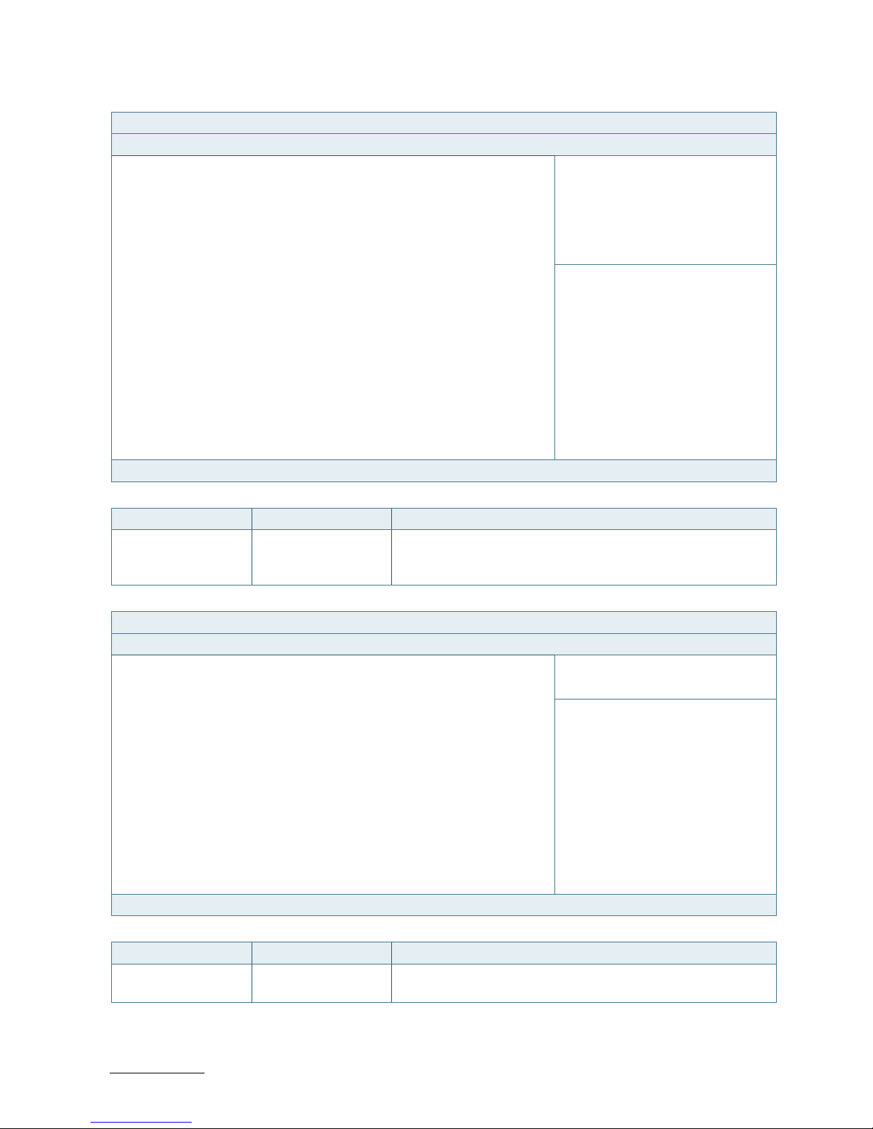
ECX-BYT - User Guide, Rev. 1.0
www.kontron.com
// 73
Figure 53: BIOS Advanced Menu - H/W Monitor
BIOS SETUP UTILITY
Main Advanced Power Boot Security Save & Exit
PC Health Status
CPU Warning Temperature [Disabled]
> CPU FAN Configuration
CPU Temperature : +40 C
→ ←: Select Screen
System Temperature : +39 C
↑ ↓: Select Item
Enter: Select
CPU Fan Speed : N/A +/-: Change Opt.
F1: General Help
+VCORE : +0.773 V F2: Previous Values
+VIN : +12.268 V F3: Optimized Defaults
+5V : +5.066 V F4: Save & Exit
+VMEN : +1.357 V ESC: Exit
Version 2.16.1242. Copyright (C) 2013, American Megatrends, Inc.
Feature Option Description
CPU Warning
Temperature
[Disabled], [80], [85],
[90], [95]
Determine whether to enable or disable CPU Warning
Temperature function and select a temperature that will sound
an alarm.
BIOS SETUP UTILITY
Main Advanced Power Boot Security Save & Exit
CPU FAN Configuration
FAN Setting [Manual Mode]
→ ←: Select Screen
Manual Duty 255
↑ ↓: Select Item
Enter: Select
+/-: Change Opt.
F1: General Help
F2: Previous Values
F3: Optimized Defaults
F4: Save & Exit
ESC: Exit
Version 2.16.1242. Copyright (C) 2013, American Megatrends, Inc.
Feature Option Description
FAN Setting [Manual Mode], [Auto
Mode]
Switch the CPU FAN control mode.
Page 74

ECX-BYT - User Guide, Rev. 1.0
www.kontron.com
// 74
9.2.3. Power Setup Menu
The Power setup menu provides functions and a sub-screen for power configurations. The following sub-screen
function is included in the menu:
WatchDog Timer Configuration
Figure 54: BIOS Power Setup Menu
BIOS SETUP UTILITY
Main Advanced Power Boot Security Save & Exit
Power Management Configuration
ACPI Sleep State [S3 (Suspend to RAM)]
Restore AC Power Loss [Power Off]
Power Saving Mode [Disabled]
→ ←: Select Screen
↑ ↓: Select Item
Resume Event Control Enter: Select
Resume From S3 By PS/2 Keyboard [Disabled] +/-: Change Opt.
Resume From S3 By PS/2 Mouse [Disabled] F1: General Help
Resume By PCIE Device [Disabled] F2: Previous Values
Resume By Ring Device [Disabled] F3: Optimized Defaults
Resume By RTC Alarm [Disabled] F4: Save & Exit
> WatchDog Time Configuration ESC: Exit
Version 2.16.1242. Copyright (C) 2013, American Megatrends, Inc.
Feature Option Description
ACPI Sleep State [Suspend Disabled],
[S1 (CPU Stop Clock)],
{S3 (Suspend to
RAM)]
Select whether to enable or disable suspend function and
determine an appropriate suspend mode.
Restore AC Power
Loss
[Power Off], [Power
On], [Last State]
Control whether the system will stay on after AC power is
removed and then restored.
Select [Power Off] if you want the system to remain off after
power restored.
Select [Power On] if you use a power strip to turn the system on.
Power Saving Mode [Disabled], [Enabled] Select whether to enable Power Saving Mode.
Resume From S3 By
PS/2 Keyboard
[Enabled], [Disabled] Select whether to allow wakening the system up from the S3
sleep state by PS/2 keyboard.
Resume From S3 By
PS/2 Mouse
[Enabled], [Disabled] Select whether to allow wakening the system up from the S3
sleep state by PS/2 mouse.
Resume By PCIE
Device
[Disabled], [Enabled] Select whether to enable or disable Wake from PCIE Device.
Resume By Ring
Device
[Disabled], [Enabled] Select whether to enable or disable Wake from Ring Device.
Resume By RTC Alarm [Disabled], [Enabled] Select whether to enable or disable Wake Up on Alarm, to turn
on your system on a special day of the month.
Page 75

ECX-BYT - User Guide, Rev. 1.0
www.kontron.com
// 75
Figure 55: BIOS Power Setup Menu - WatchDog Timer Configuration
BIOS SETUP UTILITY
Main Advanced Power Boot Security Save & Exit
WatchDog Timer Configuration
WDT Function [Disabled]
→ ←: Select Screen
↑ ↓: Select Item
Enter: Select
+/-: Change Opt.
F1: General Help
F2: Previous Values
F3: Optimized Defaults
F4: Save & Exit
ESC: Exit
Version 2.16.1242. Copyright (C) 2013, American Megatrends, Inc.
Feature Option Description
WDT Function [Disabled], [Enabled] Select whether to enable or disable WatchDog Timer function.
Page 76
ECX-BYT - User Guide, Rev. 1.0
www.kontron.com
// 76
9.2.4. Boot Setup Menu
The boot setup menu lists the for boot device priority order, that is generated dynamically.
Figure 56: BIOS Boot Setup Menu
BIOS SETUP UTILITY
Main Advanced Power Boot Security Save & Exit
Boot Configuration
Full Screen LOGO Display [Disabled]
Setup Prompt Timeout 1
→ ←: Select Screen
Bootup NumLock State [On]
↑ ↓: Select Item
Keyboard Detect Warning [Enabled] Enter: Select
+/-: Change Opt.
CSM Support [Enabled] F1: General Help
Boot Option Filter [Legacy Only] F2: Previous Values
F3: Optimized Defaults
Boot Option Priorities F4: Save & Exit
ESC: Exit
Version 2.16.1242. Copyright (C) 2013, American Megatrends, Inc.
Feature Option Description
Full Screen LOGO
Display
[Disabled], [Enabled] Select whether to enable or disable to display logo screen.
Bootup NumLock
State
[On], [Off] Select the state of the NumLock feature of the keyboard after
Startup.
[On]: The keys on the keypad will act as numeric keys.
[Off]: The keys on the keypad will act as cursor keys.
Keyboard Detect
Warning
[Disabled], [Enabled] Select whether to enable or disable Keyboard Detect Warning
function.
CSM Support [Enabled], [Disabled] Select whether to enable or disable CSM support.
Boot Option Filter [UEFI and Legacy],
[Legacy only], [UEFI
only]
Control Legacy / UEFI ROMs priority.
Page 77
ECX-BYT - User Guide, Rev. 1.0
www.kontron.com
// 77
9.2.5. Security Setup Menu
The Security setup menu provides information about the passwords and functions for specifying the security settings.
The passwords are case-sensitive. The ECX-BYT provides no factory-set passwords.
If there is already a password installed, the system asks for this first. To clear a
password, simply enter nothing and acknowledge by pressing <RETURN>. To set a
password, enter it twice and acknowledge by pressing <RETURN>.
Figure 57: BIOS Boot Setup Menu
BIOS SETUP UTILITY
Main Advanced Power Boot Security Save & Exit
Password Description
If ONLY the Administrator’s password is set, then this only limits access to
Setup and is only asked for when entering Setup
If ONLY the User’s password is set, then this is a power on password and
must be entered to boot or enter Setup. In Setup the User will have
Administrator rights
The password length must be in the following range:
→ ←: Select Screen
Minimum Length 3
↑ ↓: Select Item
Maximum length 20 Enter: Select
+/-: Change Opt.
Administrator Password F1: General Help
User Password F2: Previous Values
F3: Optimized Defaults
HDD Security Configuration: F4: Save & Exit
HDD 0: WDC WD 1600BE ESC: Exit
Version 2.16.1242. Copyright (C) 2013, American Megatrends, Inc.
Feature Description
Administrator Password Set administrator password
User Password Set user password
If only the administrator’s password is set, then only access to setup is limited. The
password is only entered when entering setup.
If only the user’s password is set, then the password is a power on password and must
be entered to boot or enter setup. Within the setup menu the user has administrator
rights.
Password length requirements are maximum 20 characters and minimum 3 characters.
Page 78

ECX-BYT - User Guide, Rev. 1.0
www.kontron.com
// 78
9.2.5.1. Remember the password
It is highly recommended to keep a record of all passwords in a safe place. Forgotten passwords results in being
locked out of the system.
If the system cannot be booted because the User Password or the Supervisor Password are not know, contact
Kontron Support for further assistance.
HDD security passwords cannot be cleared using the above method.
Page 79
ECX-BYT - User Guide, Rev. 1.0
www.kontron.com
// 79
9.2.6. Save & Exit Setup Menu
The exit setup menu provides functions for handling changes made to the UEFI BIOS settings and the exiting of the
setup program.
Figure 58: BIOS Boot Setup Menu
BIOS SETUP UTILITY
Main Advanced Power Boot Security Save & Exit
Save Changes and Reset
Discard Changes and Reset
→ ←: Select Screen
Save Options
↑ ↓: Select Item
Save Changes Enter: Select
Discard Changes +/-: Change Opt.
F1: General Help
Restore Defaults F2: Previous Values
F3: Optimized Defaults
F4: Save & Exit
ESC: Exit
Version 2.16.1242. Copyright (C) 2013, American Megatrends, Inc.
Feature Description
Save Changes and
Exit
Exit system setup after saving the changes. Once you are finished making your
selections, choose this option from the Exit menu to ensure the values you selected are
saved to the CMOS RAM. The CMOS RAM is sustained by an onboard backup battery and
stays on even when the PC is turned off. When you select this option, a confirmation
window appears. Select [Yes] to save changes and exit.
Discard Changes and
Exit
Exit system setup without saving any changes. Select this option only if you do not want
to save the changes that you made to the Setup program. If you made changes to fields
other than system date, system time, and password, the BIOS asks for a confirmation
before exiting.
Save Changes Save changes done so far to any of the setup values. This option allows you to save the
selections you made. After selecting this option, a confirmation appears. Select [Yes] to
save any changes.
Discard Changes Discards changes done so far to any of the setup values. This option allows you to
discard the selections you made and restore the previously saved values. After selecting
this option, a confirmation appears. Select [Yes] to discard any changes and load the
previously saved values.
Restore Defaults Restore Default values for all the setup values. This option allows you to load optimal
default values for each of the parameters on the Setup menus, which will provide the
best performance settings for your system. The F9 key can be used for this operation.
Page 80

ECX-BYT - User Guide, Rev. 1.0
www.kontron.com
// 80
Appendix A: List of Acronyms
The following table does not contain the complete acronyms used in signal names,
signal type definitions or similar. A description of the signals is included in the I/O
Connector and Internal connector chapters within this user guide.
Table 57: List of Acronyms
2D Two-Dimensional
3D Three-Dimensional
AT Advanced Technology
ATX Advanced Technology eXtended
BGA Ball Grid Array
BIOS Basic Input / Output System
BSP Board Support Package
CMOS Complementary Metal Oxide
Semiconductor
CPU Central Processing Unit
DC Direct Current
DDC Display Data Channel
DIO Digital Input / Output
ECC Error-Correcting Code
EEE Electrical and Electronic Equipment
EOS Electrical OverStress
ESD ElectroStatic Discharge
GbE Gigabit Ethernet
HDD Hard Disk Drive
HDMI High Definition Multimedia Interface
LAN Local Area Network
LED Light Emitting Device
LVDS Low-Voltage Differential Signaling
ME F/W Management Engine Firmware
mPCIe mini Peripheral Component Interconnect
express
PC-AT Personal Computer - Advanced
Technology
PCB Printed Circuit Board
PSU Power Supply Unit
PVC PolyViny Chloride
PWM Pulse Width Modulation
RAM Random Access Memory
ROM Read-Only Memory
RTC Real-Time Clock
SATA Serial Advanced Technology Attachment
SDP Serial Download Protocol
SELV Safety Extra-Low Voltage
SIM Subscriber Identity Module
SMBus System Management Bus
SoC System on Chip
SO-DIMM Small Outline Dual In-line Memory
Module
SPD Serial Presence Detect
SPI Serial Peripheral Interface
TDP Thermal Design Power
TPM Trusted Platform Module
UEFI Unified Extensible Firmware Interface
USB Universal Serial Bus
UTP Update Transfer Protocol
VGA Video Graphics Array
WDT WatchDog Timer
WEEE Waste Electrical and Electronic
Equipment
Page 81

ECX-BYT – User Guide, Rev. 1.0
www.kontron.com
// 81
About Kontron
Kontron is a global leader in embedded computing technology (ECT). As a part of technology group S&T,
Kontron offers a combined portfolio of secure hardware, middleware and services for Internet of
Things (IoT) and Industry 4.0 applications. With its standard products and tailor-made solutions based
on highly reliable state-of-the-art embedded technologies, Kontron provides secure and innovative
applications for a variety of industries. As a result, customers benefit from accelerated time-to-market,
reduced total cost of ownership, product longevity and the best fully integrated applications overall.
Kontron is a listed company. Its shares are traded in the Prime Standard segment of the Frankfurt Stock
Exchange and on other exchanges under the symbol "KBC". For more information, please visit:
www.kontron.com
CORPORATE OFFICES
EUROPE, MIDDLE EAST
& AFRICA
NORTH AMERICA
ASIA PACIFIC
Lise-Meitner-Str. 3-5
86156 Augsburg
Germany
Tel.: + 49 821 4086-0
Fax: + 49 821 4086-111
info@kontron.com
9477 Waples Street
San Diego, CA 92121
USA
Tel.: + 1 888 294 4558
Fax: + 1 858 677 0898
info@us.kontron.com
1~2F, 10 Building, No. 8 Liangshuihe 2nd Street,
Economical & Technological Development Zone,
Beijing, 100176, P.R. China
Tel.: + 86 10 63751188
Fax: + 86 10 83682438
info@kontron.cn
 Loading...