

Page 1
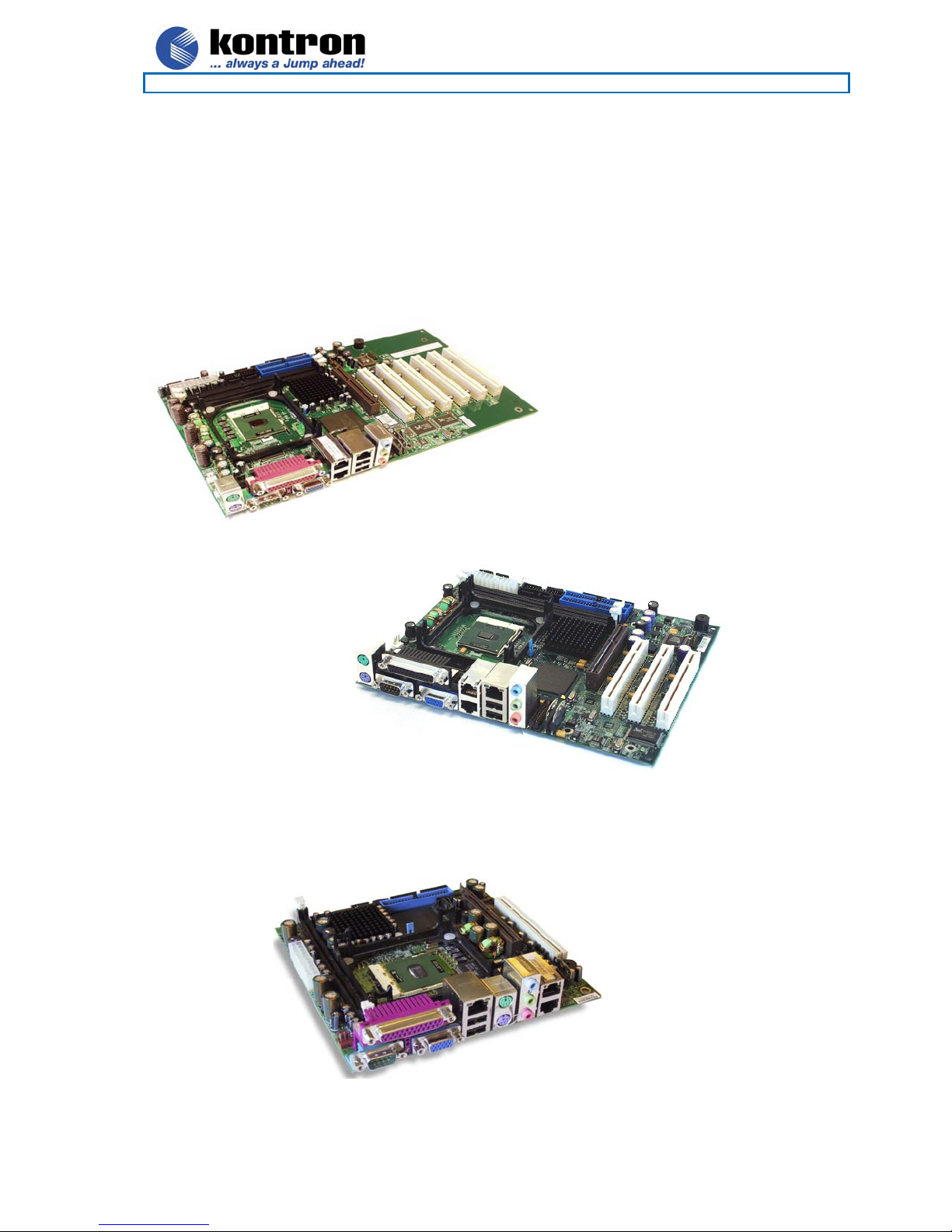
886LCD-M Family
KTD-00474-E Public User Manual Date: 2005-05-24 Page 1 of 78
User Manual
for the Mother Boards:
886LCD-M/ATX
886LCD-M/Flex
886LCD-M/mITX
Page 2
886LCD-M Family
KTD-00474-E Public User Manual Date: 2005-05-24 Page 2 of 78
Document revision history.
Revision Date By Comment
E May. 24th, 2005 PJA/MLA Major revision. BIOS information added.
D Dec. 20th, 2004 PJA 886LCD-M/ATX information ad de d
C Dec. 13th, 2004 PJA 886LCD-M/mITX information added
A Sept. 27th, 2004 MLA Many correction and added information, but still preliminary
0.1 June 14th, 2004 PJA First preliminary manual version.
Copyright Notice:
Copyright © 2005, KONTRON Technology A/S, ALL RIGHTS RESERVED.
No part of this document may be reproduced or transmitted in any form or by any means, electronically or
mechanically, for any purpose, without the express written permission of KONTRON Technology A/S.
Trademark Acknowledgement:
Brand and product names are trademarks or registered trademarks of their respective owners.
Disclaimer:
KONTRON Technology A/S reserves the right to make changes, without notice, to any product, including
circuits and/or software described or contained in this manual in order to improve design and/or
performance.
Specifications listed in this manual are subje ct to change without notice. KONTRON Technol og y assume s
no responsibility or liability for the use of the described product(s), conveys no license or title under any
patent, copyright, or mask work rights to these products, and makes no representations or warranties that
these products are free from patent, cop yright, or mask work right infringement, unless otherwise specified.
Applications that are described in this manual are for illustration purposes only. KONTRON Technology A/S
makes no representation or warranty that such application will be suitable for the specified use without
further testing or modification.
Page 3

886LCD-M Family
KTD-00474-E Public User Manual Date: 2005-05-24 Page 3 of 78
Life Support Policy
KONTRON Technology’s PRODUCTS ARE NOT FOR USE AS CRITICAL COMPONENTS IN LI FE
SUPPORT DEVICES OR SYSTEMS WITHOUT EXPRESS WRITTEN APPROVAL OF THE GENERAL
MANAGER OF KONTRON Technology A/S.
As used herein:
1. Life support devices or systems are devices or system s wh ich, (a) are intended for surgical implant into
body, or (b) support or sustain lif e an d whose failure to perform, when properl y used in accordance with
instructions for use provided in the labeling, can be reasonably expected to result in significant injury to
the user.
2. A critical component is any component of a life support device or system whose failure to perform can be
reasonably expected to cause the failure of the life support device or system, or to affect its safety or
effectiveness.
KONTRON Technology Technical Support and Services
If you have questions about installing or using your KONTRON Technology Pro du c t , check this User’s
Manual first – you will find answers to most questions here. To obtain support, please contact your local
Distributor or Field Application Engineer (FAE).
Before Contacting Support: Please be prepared to provide as much information as possible:
CPU Board
1. Type.
2. Part-number (Number starting with “53”).
3. Serial Number.
Configuration
1. CPU Type, Clock speed.
2. DRAM Type and Size.
3. BIOS Revision (Find the Version Info in the BIOS Setu p in th e Kontron Section).
4. BIOS Settings different than Default Settings (Refer to the Software Manual).
System
1. O/S Make and Version.
2. Driver Version numbers (Gra ph ics, Network, and Audio).
3. Attached Hardware: Harddisks, CD-rom, LCD Panels etc.
Page 4

886LCD-M Family
KTD-00474-E Public User Manual Date: 2005-05-24 Page 4 of 78
Table of contents:
1.
INTRODUCTION.....................................................................................................................................7
2. INSTALLATION PROCEDURE..............................................................................................................8
2.1 Inst alling the board.................. ..........................................................................................................8
2.2 Requirement according to EN60950 ...................... ............................................... ...........................9
3. SYSTEM SPECIFICATION...................................................................................................................10
3.1 Component main data .....................................................................................................................10
3.2 Processor support table..................................................................................................................13
3.3 System Memory support .................................................................................................................13
3.4 System overview..............................................................................................................................14
3.5 886LCD-M Power Distribution & Power State Map ......................................................................15
3.6 Power Consumption........................................................................................................................17
3.6.1 Test system configuration...........................................................................................................17
3.6.2 Measured Power Consumption, Net...........................................................................................17
3.6.3 Power Consumption, Total .........................................................................................................18
3.6.4 Minimum recommended power supply specifications................................................................18
3.6.5 Recommended Power Supply specifications .............................................................................18
3.7 886LCD-M Clock Distribution ................................................ .........................................................19
4. CONNECTOR DEFINITIONS................................................................................................................21
4.1 Connector layout..............................................................................................................................22
4.1.1 886LCD-M/Flex...........................................................................................................................22
4.1.2 886LCD-M/ATX ..........................................................................................................................23
4.1.3 886LCD-M/mITX.........................................................................................................................24
4.2 Power Connector (ATXPWR)..........................................................................................................24
4.2 Power Connector (ATXPWR)..........................................................................................................25
4.3 Keyboard and PS/2 mouse connectors.........................................................................................26
4.3.1 Stacked MINI-DIN keyboard and mouse Connector (MSE & KBD)...........................................26
4.3.2 keyboard and mouse pin-row Connector (KBDMSE).................................................................26
4.4 Display Connectors .........................................................................................................................27
4.4.1 CRT Connector (CRT)................................................................................................................27
4.4.2 LVDS Flat Panel Connector (LVDS)...........................................................................................28
4.4.3 AGP/DVO connector...................................................................................................................29
4.5 Parallel ATA harddisk interface......................................................................................................33
4.5.1 IDE Hard Disk Connector (IDE_P) ...................................................................................... .......34
4.5.2 IDE Hard Disk Connector (IDE_S) ...................................................................................... .......34
4.5.3 IDE Hard Disk Connector (IDE_S2) ............................................. ........................................... ...35
4.5.4 CF Connector (CF) .....................................................................................................................36
4.6 Serial ATA harddisk interface.........................................................................................................37
4.6.1 SATA Hard Disk Connector (SATA0, SATA1) ...........................................................................37
Page 5

886LCD-M Family
KTD-00474-E Public User Manual Date: 2005-05-24 Page 5 of 78
4.7
Printer Port Connector (PRINTER).................................................................................................38
4.8 Serial Ports .......................................................................................................................................39
4.8.1 Serial Port ComA DB9 Connector. .............................................................................................39
4.8.2 Serial Port ComB, ComC & ComD Pin Header Connectors. .....................................................39
4.9 Ethernet connectors........................................................................................................................40
4.9.1 Ethernet connector 1 (ETHER1).................................................................................................40
4.9.2 Ethernet connector 2/3 (ETHER2/3)...........................................................................................41
4.10 USB Connector (USB)..................................................................................................................42
4.10.1 USB Connector 0/2 (USB0/2).....................................................................................................42
4.11 Audio Connector ..........................................................................................................................43
4.11.1 Audio Line-in, Line-out and Microphone.....................................................................................43
4.11.2 CD-ROM Audio input (CDROM).................................................................................................43
4.11.3 AUDIO Header (AUDIO_HEAD).................................................................................................44
4.12 Fan connectors , FAN_PROC and FAN_SYS. ...........................................................................45
4.13 The Clear CMOS Jumper, Clr-CMOS..........................................................................................45
4.14 LPC connector (unsupported). ...................................................................................................45
4.15 Front Panel connector (FRONTPNL)..........................................................................................46
4.16 Intruder Connector (INT)..............................................................................................................46
4.17 Feature Connector (FEATURE)...................................................................................................47
4.17.1 PCI Slot Connector....................................................................................................................48
4.17.2 Signal Description –PCI Slot Co nnector.......................................................................... ...........49
4.17.3 886LCD-M PCI IRQ & INT routing..............................................................................................50
5. ONBOARD CONNECTORS ............................................................................................ .....................51
6. SYSTEM RESSOURCES......................................................................................................................52
6.1 Memory map.....................................................................................................................................52
6.2 PCI devices.......................................................................................................................................52
6.3 Interrupt Usage ................................................................................................................................53
6.4 I/O Map ..............................................................................................................................................54
6.5 DMA Channel Usage........................................................................................................................54
7. OVERVIEW OF BIOS FEATURES.......................................................................................................55
7.1.1 System Management BIOS (SMBIOS / DMI).............................................................................55
7.1.2 Legacy USB Support ..................................................................................................................55
8. BIOS CONFIGURATION / SETUP .......................................................................................................56
8.1 Introduction......................................................................................................................................56
8.2 Main Menu.........................................................................................................................................56
8.3 Advanced Menu................................................................................................................................57
8.3.1 Advanced settings – CPU Configuration....................................................................................57
8.3.2 Advanced settings – IDE Configuration......................................................................................58
Page 6

886LCD-M Family
KTD-00474-E Public User Manual Date: 2005-05-24 Page 6 of 78
8.3.3
Advanced settings – LAN Configuration.....................................................................................60
8.3.4 Advanced settings – Floppy Configuration.................................................................................61
8.3.5 Advanced settings – SuperIO Configuration ..............................................................................62
8.3.6 Advanced settings – Hardware Health Configuration ................................................................63
8.3.7 Advanced settings – ACPI Configuration ...................................................................................64
8.3.8 Advanced settings – General ACPI Configuration .....................................................................64
8.3.9 Advanced settings – Advanced ACPI Configuration..................................................................65
8.3.10 Advanced settings – Remote Access Configuration ..................................................................65
8.3.11 Advanced settings – USB Configuration ....................................................................................66
8.3.12 Advanced settings – USB Mass Storage Device Configuration.................................................67
8.4 PCIPnP Menu....................................................................................................................................68
8.5 Boot Menu.........................................................................................................................................69
8.5.1 Boot – Boot Settings Configuration ............................................................................................69
8.6 Security Menu...................................................................................................................................70
8.7 Chipset Menu.................................................................................................................. ..................71
8.7.1 Advanced Chipset Settings – Intel Montara-GML NorthBridge Configuration ...........................72
8.7.2 Advanced Chipset Settings – SouthBridge Configuration..........................................................73
8.8 Power Menu......................................................................................................................................74
8.9 Exit Menu..........................................................................................................................................75
8.10 AMI BIOS Beep Codes .................................................................................................................76
9. OS SETUP.............................................................. ........................................... ....................................77
10. WARRANTY..........................................................................................................................................78
Page 7

886LCD-M Family
KTD-00474-E Public User Manual Date: 2005-05-24 Page 7 of 78
1. Introduction
This manual describes the 886LCD-M/Fle x, 886LCD-M/ATX and 886LCD-M/mITX boards made by
KONTRON Technology A/S. The boards will also be den oted 886LCD family if no differentiation is required.
All boards are to be used with the Intel® Pentium® M & Intel Celeron® M Processors.
Use of this manual implies a basic knowledge of PC-AT ha rd- and software. This manual is focused on
describing the 886 Board’s special feat ur es and is not intended to be a standard PC-A T textbook.
New users are recommended to study the short installation procedure stated in chapter 3 before switching-
on the power.
All configuration and setup of the CPU board is either done automatically or by the user in the CMOS setup
menus. Except for the CMOS Clear jumper, no jumper configuration is required.
Page 8

886LCD-M Family
KTD-00474-E Public User Manual Date: 2005-05-24 Page 8 of 78
2. Installation procedure
2.1 Installing the board
To get the board running, follow these ste ps. In some cases the board shipped from KONTRON Techno log y
has CPU, DDR DRAM and Cooler mounted. In this case Step 2-4 can be skipped.
1. Turn off the power supply.
Warning: Do not use Power Supply without 3.3V mon itoring watchdog, which is
!
2. Insert the DIMM DDR 184pin DRAM module(s). Be careful to push it in the sl ot(s) before locking the
tabs. For a list of approved DDR DRAM modules contact your Distributor or FAE (list under preparation).
DDR333, DIMM 184pin DRAM modules are supported.
3. Install the processor. The CPU is keyed and will only mount in the CPU socket in one way. Use the
handle to open/ close the CPU socket. Int el Pentium M and Celeron M processors (Banias processo rs)
are supported.
4. Use heat paste or adhesive pads between CPU and cooler and connect the Fan electrically to the
FAN_PROC connector.
5. Insert all external cab l es f or h ar d disk, keyboard etc. except for flat pa ne l. A CRT monitor must be
connected in order to change CMOS settings to flat panel support. To achieve UDMA-66/100/133
performance on the IDE interface, 80p oled UDMA cables must be used. If using the I DE_S2 conn ector
care should be taken in correct orientation when attaching the fe male cable. The cabl es that KONTRON
provide do not have a key. There is possibility of damage to the HDD or PCB if the cab le is not orienta ted
correctly.
standard feature in ATX Power S upplies.
Running the board without 3.3V conn ected will damage the board after a few minut e s.
Note: If the Audio Amplifiers shall be used to generate up to 3W on one or more of the
Audio ouput channels, then make sure that sufficent airflow is around the Audio
!
6. Connect power supply to the boar d by t he A TXP WR connecto r.
7. Turn on the power on the ATX power supply.
8. The PWRBTN_IN must be toggled to start the Power supply; this is done by shorting pins 16
(PWRBTN_IN) and pin 18 (GND) on the FRONTPNL connector (see Connector description). A “normally
open” switch can be connected via the FRONTPNL connect or.
9. Enter the BIOS setup by pressing t he “F2” key during boot up. Ref er to t he S oft ware Manua l (und er
preparation) for details on BIOS setu p.
Enter A dv a n c e d M e n u / C P U Co n f i g u r at i o n / Inte l SpeedStep Tech. and set this option to “Maximum
Performance”.
Note: To clear all CMOS settings, including Password protection, mov e the CMOS_CL R jumper (with or without
power) for approximately 1 m inut e. Alt ernat ive ly t ur n of f pow er and r emove the bat te ry f or 1 min ute, but be
careful to orientate the battery corret ly when reinsert ed.
Amplifier. The Amplifier has integra t ed Thermal Protection and will not be damaged
even though the airflow is insuf ficient for normal operation.
Page 9

886LCD-M Family
KTD-00474-E Public User Manual Date: 2005-05-24 Page 9 of 78
2.2 Requirement according to EN60950
Users of 886LCD boards should take care when designing chassis interface connectors in order to fulfill the
EN60950 standard:
When an interface/connector has a VCC (or other power) pin, which is directly connected to a power
plane like the VCC plane:
To protect the external power lines of pe rip he ral devices the customer has to take care abou t:
• That the wires have the right diameter to withstand the maximum available power.
• That the enclosure of the peripheral device fulfils the fire protecting requirements of IEC/EN 60950.
Lithium Battery precautions:
CAUTION!
Danger of explosion if battery is incorrectly
replaced.
Replace only with same or equivalent type
recommended by manufacturer.
Dispose of used batteries accord ing
to the manufacturer’s instructions.
ADVARSEL!
Lithiumbatteri – Eksplosionsfare ved fejlagtig
håndtering.
Udskiftning må kun ske med batteri
af samme fabrikat og type.
Levér det brugte batteri tilbage til leverandøren.
Explosionsgefahr bei unsachgemäßem Au stausch
Ersatz nur durch den selben oder einen vom
Hersteller empfohlenen gleichwertigen Ty p.
Entsorgung gebrauchter Batterien nach
Eksplosjonsfare ved feilaktig skifte av batteri.
Benytt samme batteritype eller en tilsvarende
type anbefalt av apparatfabrikanten.
Brukte batterier kasseres i henhold til fa brikantens
VORSICHT!
der Batterie.
Angaben des Herstellers.
ADVARSEL
instruksjoner.
VARNING
Explosionsfara vid felaktigt batteribyte.
Använd samma batterityp eller en ekvi v ale nt
typ som rekommenderas av apparattillverkaren.
Kassera använt batteri enligt fabrikantens
instruktion.
VAROITUS
Paristo voi räjähtää, jos se on virheellisesti
Vaihda paristo ainoastaan laltev almistajan
suosittelemaan
tyyppiln. Hävitä käytetty paristo valmistajan
asennettu.
ohjeiden
mukaisesti.
Page 10

KTD-00474-E Public User Manual Date: 2005-05-24 Page 10 of 78
3. System specification
3.1 Component main data
The table below summarises the features of the 886LCD-M/Flex, 886LCD-M/ATX and 886LCD-M/mITX
embedded motherboards.
Form factor
Processor
Memory
Chipset
Video
Audio
I/O Control
Peripheral
interfaces
886LCD-M/Flex: Flex-ATX (190,50millimeters by 228,60millimeters)
886LCD-M/ATX: ATX (190,50millimeters by 304,00millimeter s)
886LCD-M/mITX: mini ITX (170.18millimeters by 170.18millimeters)
• Support for Intel Pentium M and Celer on M Pro cesso rs in mPGA478 socket with
400MHz system bus.
• Banias (0.13um) and Dothan (0.09u m) family processors.
• For /Flex and /ATX: 2x184pin DDR SDRAM Dual Inline Memory Module (DIMM)
sockets.
• For /mITX: 1x184pin DDR SDRAM Dual In lin e Me mory Module (DIMM) sockets.
• Support for DDR 266/333 (PC2100/PC2700)
• Support for up to 2GB of system memory (/Flex and /ATX)
• Support for up to 1GB of system memory (/mITX)
• ECC support depend on Intel
Intel 855GME Chipset consisting of:
• Intel® 855GME Chipset Graphics and Memory Controller Hub (GMCH)
• Intel® 6300ESB I/O Controller Hub (ICH)
• 4 Mbit Firmware Hub (FWH)
• Intel Extreme Graphics 2 controlle r
• Analog Display Support, 35 0-MHz integrated 24-bit RAMDAC with suppor t for
analogue monitors up to 2048x15 36 at 75 Hz
• Digital Video Out Port (DVOB & DVOC) support, dot clock up to 165-MHz
• Single or dual channel LVDS panel support (18/ 24bit OpenLDI / SPWG) up to
UXGA panel resolution
• Dual independent pipe support, Mirror and Dual independent display supp or t
Tri-view support through LVDS interface, DVO B/C port, and CRT
• AGP 2.0, 1.5V connector (DV O B/C muxed w/ AGP) supporting 1x, 2x, and 4x
AGP cards or an AGP Digital Display (ADD) card
Audio, AC97 version 2.3 subsystem using the Realtek ALC655 codec
• Audio Amplifier
• Line-out
• CDROM in
• SPDIF Interface (Surround)
• Microphone
Onboard speaker
Winbond W83627THF LPC Bus I/O Contro ller
• Four USB 2.0 ports
• Four Serial ports (RS232). Note: In tel 6300ESB Serial port FIFO (COM C+D) is
not standard compliant. May cause issues wit h spe cif ic SW.
• One Parallel port, SPP/EPP /ECP / Floppy (optional floppy with specia l cab lin g)
• Two Serial ATA 150 IDE interfaces, ATA Mode 6 not supported due to Intel
Chipset restrictions.
• Two Parallel ATA IDE interfaces with UDMA 33 , ATA-66/100 support
• PS/2 keyboard and mouse ports
886LCD-M Family
DVI DVO ADD and CRT DVO ADD supported.
LVDS DVO ADD cards currently not supported
CRT – LVDS supported
CRT - DVO/ Add card supported
LVDS - DVO/ Add card supporte d
o /FLEX and /ATX: 4x3W
o /mITX: 2x3W
(continued)
Page 11

886LCD-M Family
KTD-00474-E Public User Manual Date: 2005-05-24 Page 11 of 78
LAN Support
BIOS
Instantly
Available PC
Technology
Expansion
Capabilities
Hardware
Monitor
Subsystem
Operating
Systems
Support
3x 10/100/1000Mbits/s LAN subsystem using the Realtek RTL8110SB-32 LAN
controllers or
1x / 3x 10/100Mbits/s LAN subsystem using the Realtek RTL8100C LAN controllers
depending on board configuration.
PXE and RPL netboot supporte d. Wake On LAN (WOL) supported.
• Kontron Technology / AMI BIOS (co re ve rsio n)
• Support for Advanced Configuration and Power Interface (ACPI 1.0, 2.0), Plug
and Play
o Suspend To Ram
o Suspend To Disk
o Intel Speed Step
• SW Watchdog currently not supported by BIOS
• Secure CMOS/ OEM Setup Defaults
• “Always On” BIOS power setting
• RAID Support (RAID modes 0 and 1 )
• Support for PCI Local Bus Specification Revision 2.2
• Suspend to RAM support
• SMBus routed to FEATURE connector
• LPC Bus routed to LPC connector
• DDC Bus routed to LVDS connector
• 8 x GPIOs (General Purpose I / O s) ro uted to FEATURE connector
• PCI Bus routed to PCI slot(s) (PCI Lo cal Bus Specification Revision 2.2)
• Smart Fan control system, support Thermal® and Speed® cruise for three
onboard Fan control connectors: FAN_PROC, FA N_ SYS and FEATURE
• Three thermal inputs: CPU die tempe ra tu re , System temperature and External
temperature input routed to FEA T URE connector.
• Voltage monitoring
• Intrusion detect input
SMI violations (BIOS) on HW mo nitor not supported. Supported by API (Windows).
• Win2000
• WinXP
• Win98 (USB2.0, ACPI S4 not supported)
• Win2003
• WinXP Embedded (limitations may apply)
• WinCE.net (limitations may apply)
• Linux: Feodora Core 3, Suse 9.2 (limitations may apply)
(continued)
Page 12

886LCD-M Family
KTD-00474-E Public User Manual Date: 2005-05-24 Page 12 of 78
Environmental
Conditions
Battery
Operating:
0°C – 60°C operating temperature (f orce d cooling). It is the customer’s responsibil i ty
to provide sufficient airflow aro un d ea ch of the components to keep them within
allowed temperature range.
10% - 90% relative humidity (non-condensing)
Storage:
-20°C – 70°C
5% - 95% relative humidity (non-condensing)
Electro Static Discharge (ESD) / Radiated Emissions (EMI):
All Peripheral interfaces intended for connection to external equipment are ESD/ EMI
protected.
EN 61000-4-2:2000 ESD Immunity
EN55022:1998 class B Generic Emission St an da rd .
Safety:
UL 60950-1:2003, First Edition
CSA C22.2 No. 60950-1-03 1st Ed. Apr il 1, 2003
Product Category: Information Technology Equipment Including Electrical Business
Equipment
Product Category CCN: NWGQ2, NWGQ8
File number: E194252
Theoretical MTBF:
199,799hours (22,8years) , Calculation based on Telcordia SR-332 method.
Restriction of Hazardeous Substances (RoHS):
All boards in the 886LCD-M family is planned for RoHS compliance.
Capacitor utilization:
No Tantal capacitors on board
Only Japanese brand Aluminium capacitors rat e d fo r 1 00 de gre es Ce lsius used on
board
Exchangeable 3.0V Lithium battery for onboard Real Time Clock and CMOS RAM.
Manufacturer Toshiba / Part-number CR2032.
Approximate 5 years retention.
CAUTION: Danger of explosion if the battery is incorrectly replaced. Replace
only with the same or equivalent type recommended by the manufacturer.
Dispose of used batteries according to the manufacturer’s instructions.
Page 13

886LCD-M Family
KTD-00474-E Public User Manual Date: 2005-05-24 Page 13 of 78
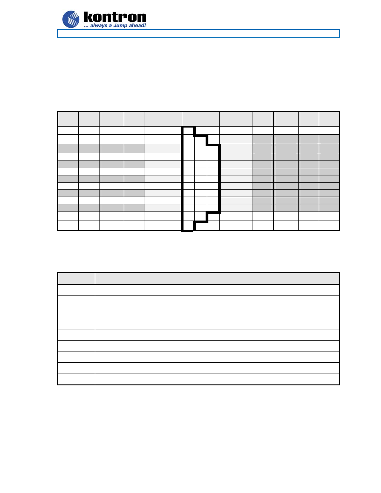
3.2 Processor support table.
886LCD-M/Flex, 886LCD-M/ATX and 886LCD-M/mITX boards are designed to support the following
processors:
Intel® Pentium® M Processor, 130 nm pro cess wit h 1 M B L2 cache
Intel® Pentium® M Processor, 90 nm process with 2 MB L2 cache
Intel®Celeron® M Processor, 130 nm process with 512 kB L2 cache
Intel®Celeron® M Processor, 90 nm process with 1 MB L2 cache
Processor Brand Processor
Number
Intel® Pentium® M 765 Dothan 90nm 2.1 GHz 400 MHz 2MB L2
755 Dothan 90nm 2.0 GHz 400 MHz 2MB L2
745 Dothan 90nm 1.8 GHz 400 MHz 2MB L2
735 Dothan 90nm 1.7 GHz 400 MHz 2MB L2
725 Dothan 90nm 1.6 GHz 400 MHz 2MB L2
RH80535GC0251M Banias 130nm 1.6 GHz 400 MHz 1MB L2
715 Dothan 90nm 1.5 GHz 400 MHz 2MB L2
705 Dothan 130nm 1. 5 G Hz 400 MHz 1MB L2
Intel® Celeron® M 370 Dothan 90nm 1.5 GHz 400 MHz 1MB L2
360 Dothan 90nm 1.4 GHz 400 MHz 1MB L2
350 Dothan 90nm 1.3 GHz 400 MHz 1MB L2
340 Banias 130nm 1.5 GHz 400 MHz 512MB L2
330 Banias 130nm 1.4 GHz 400 MHz 512MB L2
320 Banias 130nm 1.3 GHz 400 MHz 512KB L2
The above list contains PGA versions only, but also BGA versions are supported, if required please ask
Kontron for more information.
Processor
Generation
Clock
Speed
Front Side
Bus
Cache
3.3 System Memory support
The 886LCD-M/Flex and 886LCD-M/A TX boards have two onboard DIMM sockets (886LCD -M/ mITX
equipped with one DIMM socket only) and sup po rt t h e following memory features:
• 2.5V (only) 184-pin DDR SDRAM DIMMs with gold-plated contacts
• Supports up to two (one on mITX) single- side d an d/or double-sided DIMMs (four rows populate d)
with unbuffered PC1600/PC21 00 /PC2700 DDR-SDRAM (with or without ECC(de pends on Intel))
• Supports 64 Mbit, 128 Mbit, 256 Mb it and 512 Mbit technologies for x8 and x16 wid t h de vices.
• Maximum of 2 Gbytes system (1GB on mITX) memory by using 512 Mbit technology devi ce s
(double sided)
• Supports 200 MHz, 266 MHz, and 333 MHz DDR dev ices
• 64-bit data interface (72-bit with ECC(depends on Intel))
The installed DDR SDRAM should support the Ser ial Presence Detect (SPD) data structure. This allows the
BIOS to read and configure the mem or y co ntroller for optimal performance. If non-SPD memory is used, the
BIOS will attempt to configure the me mo ry settings, but performance and reliability ma y be im pa cted.
Page 14

886LCD-M Family
KTD-00474-E Public User Manual Date: 2005-05-24 Page 14 of 78
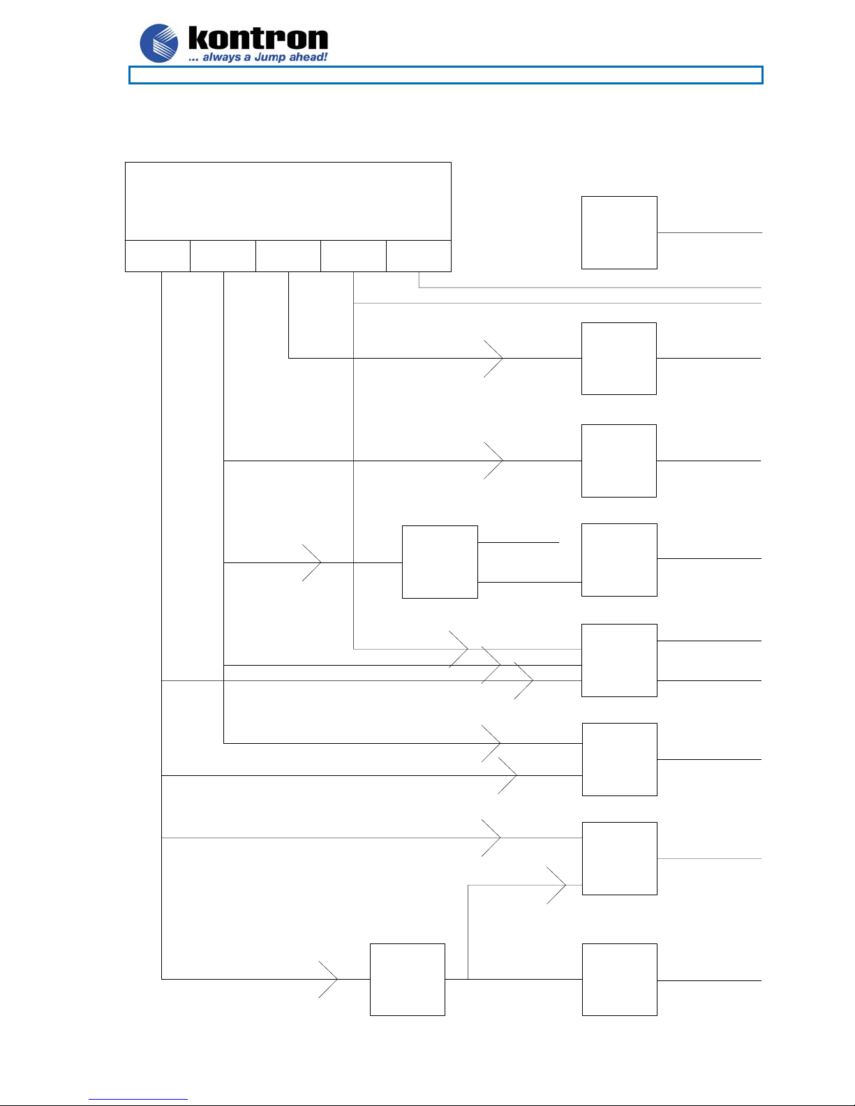
3.4 System overview
The block diagram below shows the architecture and main components of the 886LCD boards. The two key
components on the board are the I ntel
®
855GME and Intel® 6300ESB (ICH(S)) Embedded Chipsets.
Components shown shaded are optional depending on board type (886LCD-M/Flex, /ATX or /mITX) and
variants of the board.
Inte l
Processor M
Banias
& Dothan
LVDS
24 bit
HPI
DVO/
AGP
Inte l
855GM E
1x184 pins
DDR333
ECC suport
1x184 pins
DDR333
ECC suport
VGA
HUB link 1.5
PCI
PCI
PCI
PCI
10/100/
1GbE
10/100/
1GbE
10/100/
1GbE
PC I-X 32 bit, 66MHz
Inte l
ICH(S)
PC I 2.2 32 bit, 33MHz
2.2
32 bit
33
MHz
2.2
32 bit
33
MHz
2.2
32 bit
33
MHz
2.2
32 bit
33
MHz
PCI
2.2
32 bit
33
MHz
AC97
RTL655
r
R
e
+
t
L
n
t
e
n
C
o
,
r
F
F
P
L
Rear L+R
r
o
3W
amplifier3Wamplifier
AC97
KBD MSELPT
COM
#1
SIO
Winbond
W83267
THF
LPC
COM
#2
Header
LPC
4 M bit
LPC
FLASH
COM
#3
Header
COM
#4
Header
#1
#2
#3
#4
#5
2x
ATA100
2x
SATA150
2x
Internal
USB
2x
External
USB
PCI
2.2
32 bit
33
MHz
#6
Page 15
KTD-00474-E Public User Manual Date: 2005-05-24 Page 15 of 78
3.5 886LCD-M Power Distribution & Power State Map
+V5_ALWAYS +V5S +V3.3S VCC12 VCC-12
ATX PSU
Ref.: ATXPWR
886LCD-M Family
DC/DC
regulator
VCCPREG
LDO Regulator
Ref. U1SS
Ref.:
+V1.2S
+V1.5S
+V3.3ALWAYS
Battery or
+V3.3_ALWAY
S
Ref.:
BT1II
LDO Regulator
Ref. U3SS
DC/DC
regulator
Ref.:
COREREG
LDO regulator
Ref.:
VCCPAMP
DC/DC
regulator
Ref.:
ACPICTRL
MOSFET
SWITCH
Ref.: 1SD, 7SD
MOSFET
SWITCH
Ref.: 1SD, 7SD
LDO Regulator
Ref. U2SS
+V_RTC
VCC-12
VCC12
+V1.8S
+VCC_CORE
+VCCP
+V2.5
+V1.25S
+V5_DUAL
+V3.3_DUAL
+V1.5ALWAYS
(continued)
Page 16
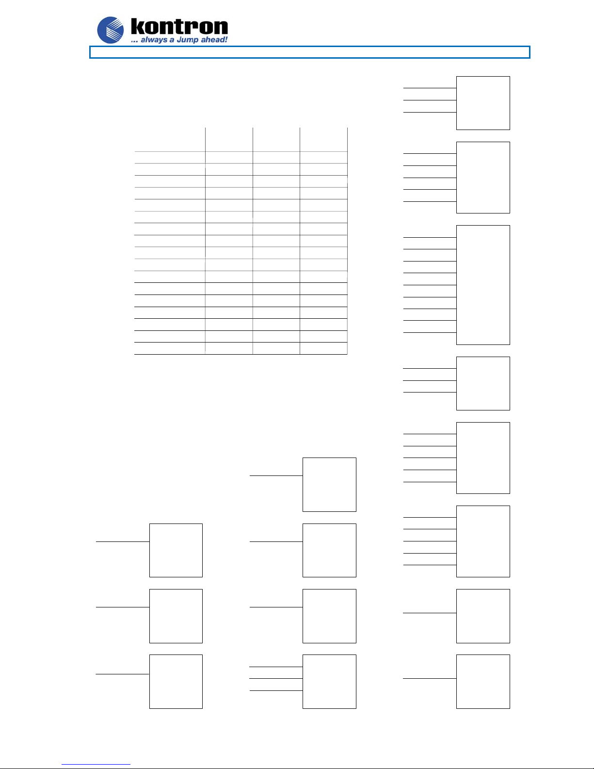
886LCD-M Family
KTD-00474-E Public User Manual Date: 2005-05-24 Page 16 of 78
+V5S
+V3.3S
VCC12
VCC-12
+V1.8S
+VCC_CORE
+VCCP
+V1.2S
+V1.5S
+V2.5
+V1.25S
+V5_DUAL
+V3.3_DUAL
+V5_ALWAYS
+V3.3ALWAYS
+V1.5ALWAYS
+V_RTC
S0
+VCC_CORE
+VCCP
+V1.8S
S3
X
X
X
X
X
X
X
X
X
X
X
X
X
X
X
X
X
N/A
N/A
N/A
N/A
N/A
N/A
N/A
N/A
N/A
X
N/A
X
X
X
X
X
X
S5
N/A
N/A
N/A
N/A
N/A
N/A
N/A
N/A
N/A
N/A
N/A
N/A
N/A
N/A
N/A
N/A
X
+VCCP
+V1.2S
+V1.5S
+V2.5
+V3.3S
+V5S
+V3.3S
+V1.5S
+VCCP
+V_RTC
+V5_ALWAYS
+V3.3_ALWAYS
+V1.5_ALWAYS
+V3.3_DUAL
+V2.5
+V1.25S
+V3.3S
Processor
Ref.:
BANIAS_
North Bridge
Ref.:
GMCH_
South Bridge
Ref.:
ICHS_
DDR Memory
Ref.:
DDRX
VCC12
+V3.3S
AC97 Codec
Ref.:
Codec
Audio
Amplifiers
Ref.:
U1A1, U1A2
BIOS Flash
Ref.:
FWH
+V5_DUAL
+V5_DUAL+V3.3S
+V5S
+V5S
VCC12
VCC-12
USB
connectors
Ref.:
USB_ETH,
FRONTPNL
KBD / MSE
Ref.:
KBD_MSE
LPT port
Ref.:
CRT_COMA_L
PT_
COM drivers
Ref.:
COMXDRV
+V1.5S
+V3.3S
+V5S
VCC12
+V3.3_ALWAYS
+V3.3S
+V5S
VCC12
VCC-12
+V3.3_ALWAYS
+V3.3_DUAL
+V3.3S
AGP
Ref.:
AGP
PCI slots
Ref.:
PCIX
Ethernet
Controllers
Ref.:
ETH1
Ethernet
Controllers
Ref.:
ETH2, ETH3
Page 17
886LCD-M Family
KTD-00474-E Public User Manual Date: 2005-05-24 Page 17 of 78
3.6 Power Consumption
This section lists a summary of the power consumption of the 886LCD-M Boards. For addi tional details,
please refer to the Power Supply Ch aracteristics document available fro m Ko ntron Technology.
The idle/full power consumption of the 886LCD-M is measured under:
1- DOS prompt idle/full CPU load.
2- WindowsXP idle/full CPU load.
3.6.1 Test system configuration
The following items were used in the test setup:
1. 886LCD-M/Flex board (710180-4500), mounted with 256MB SDRAM (333MHz) EZ128DDR16M168333INF.
2. Pentium-M 1600/600Mhz, FSB 400Mhz (1MB Cache) CPU.
3. Standard Pentium-4 active CPU cooler.
4. PS/2 keyboard & mouse.
5. CRT.
6. Primary Master HD (Fujitsu MPG3102AT 10.24GB).
7. ATX PSU (Antec 550W)
8. Tektronix TDS 620B, P6243 probes
9. Fluke Current Probe 80i-100S AC/DC
10. Ethernet Ports 1, 2, 3 are enabled (10/100/1000MB LA N ).
3.6.2 Measured Power Consumption, Net
886LCD-M board (3x1GB LAN) with: Pentium M 1600/400MHz (1MB L2 Cache), 256MB DDR RAM
(333MHz)
Power State Net Current (I) Power (W)
DOS FULL LOAD
DOS IDLE
ACPI S1
ACPI S3
ACPI S4
ACPI S5
WINDOWS XP IDLE
WINDOWS XP FULL LOAD
+5VDC 4.560A 22.8W
+3.3VDC 2.568A 8.7W
+5VDC 4.028A 20.3W
+3.3VDC 2.532A 8.6W
+12VDC 0.424A 4.6W
+5VDC 1.758A 8.8W
+3.3VDC 2.560A 8.8W
+5VSB 1.007A 5.16W
+5VSB 1.007A 4.95W
+5VSB 0.892A 4.6W
+5VDC 2.212A 11.1W
+3.3VDC 2.720A 8.7W
+5VDC 4.704A 23.7W
+3.3VDC 2.572A 8.7W
Page 18
886LCD-M Family
KTD-00474-E Public User Manual Date: 2005-05-24 Page 18 of 78
3.6.3 Power Consumption, Total
886LCD-M board (3x1GB LAN) with Pentium M 1600/400MHz (1MB L2 Cache), 256MB DDR RAM
(333MHz)
Power State CPU Speed Power consumption
Full load 1600Mhz 37.0W
Idle 1600Mhz 24.4W
ACPI S1 1600Mhz 22.2W
ACPI S3 1600Mhz 5.16W
ACPI S4 1600Mhz 4.95W
ACPI S5 1600Mhz 4.60W
886LCD-M board (3x1GB LAN) with Intel Mobile Celeron 600/400MHz (0MB L2 Cache) BG A, 256MB DDR
RAM (333MHz)
Power State CPU Speed Power consumption
Full load 600Mhz 28.4W
Idle 600Mhz 22.8W
ACPI S1 600Mhz 21.6W
ACPI S3 600Mhz 5.16W
ACPI S4 600Mhz 4.95W
ACPI S5 600Mhz 4.60W
3.6.4 Minimum recommended power supply specifications
Note: Minimum recommended power supply specifications do not include attachment of AUDIO Sp eakers
(AMP-out), USB, AGP, P CI devices. If these devices are added to the board, additional pow er re qu irements
must be taken into account. Refer to the “Detailed Device Power consumption” section.
Net Current (I) Peak Current
+5VDC 8.0A 40.0A(3ms)
+3.3VDC 4.0A 14.0A(3ms)
+12VDC 0.6A 6.0A(4ms)
+5VSB 1.2A 3.5A(14ms)
-12 VDC 0.2A 1.0A(4ms)
-5VDC N/A N/A
3.6.5 Recommended Power Supply specifications
Note: Recommended power supply specifications, includes attachment of COM, Fan, 4xAudio Speakers
4/8ohm, USB, AGP, PCI devices.
Net Current (I) Peak Current
+5VDC 18.0A 50.0A(3ms)
+3.3VDC 7.0A 20.0A(3ms)
+12VDC 6.0A 8.0A(4ms)
+5VSB 2.0A 5.0A(14ms)
-12 VDC 0.5A 1.0A(4ms)
-5VDC N/A N/A
Page 19

KTD-00474-E Public User Manual Date: 2005-05-24 Page 19 of 78
3.7 886LCD-M Clock Distribution
14.318 MHz
R e f.: Q 1 C
VR_PWRGD_CK#
HOST CLOCK PAIRS
A G P, G MCH, IC H S, PCIX
SATA CLOCK PAIR
P C I, L P C, FWH, SIO
Clock Generator
R e f.:C L K GE N
100MH z
100MH z
100MH z
66MH z
66MH z
66MH z
66MH z
66MH z
100MH z
33MH z
33MH z
33MH z
33MH z
48MH z
48MH z
14.318MHz
14.318MHz
886LCD-M Family
CLK_CPU_BCLK & CLK_CPU_BCLK#
CLK_I TP_CPU & CLK_ITP_CPU#
CLK_MCH_BCLK & CLK_MCH_BCLK#
DREFSSCLK
DREFCLK
CLK_MCH66
CLK_ICHPCI
CK_66M _AG P
CLK_3V 66_PCIX
CLK100P_SATA & CLK100P_SATA#
CLK_ICH14
CLK_ICHPCI
CLK_PCI_SLX
48MC LK
CLK_CODEC
CLK_FWHPCI
CLK_SIOPCI
Processor
R e f.: B a n ia s_
North Bridge
R e f.: G MCH _
AGP
R e f.: A GP
South Bridge
R e f.: IC HS_
PCI Sl ots
R e f.: P C IX
BIOS FLASH
R e f.: F WH
Super I/O
R e f.: L P C IO
Clock buffer
Ref.:
CLKG EN48M
AC97
CODEC
R e f.: C o d e c
(continued)
Page 20
886LCD-M Family
KTD-00474-E Public User Manual Date: 2005-05-24 Page 20 of 78
CRT VGA
Ref.:
CRT_COMA
_LPT_
North Bridge
Ref.: GMCH_
South Bridge
Re f.: ICHS_
DAC_DDCACLK
M_CLK_DDRX & M_CLK_DDRX#
LVDS_C LKX & LVD S_ CLK X#
LVDS_D DCPC LK
Real Time
Clock
32.768
Ref.: Q1 II
PXPCLKO#
DDR Memory
Re f.: DDR0 ,
DDR1
LVDS
Inte rfa c e
Ref.: L V DS
25 MHz
Re f. : Y 1 EX
ETHERNET
controllers
Re f. : E TH #
Su p er I/O
Re f.: LP CIO
Clock buffer
Re f.:
CLKGEN48M
AC97
CODEC
Ref.: C od e c
CLK_SIO48
AC97_BITCLK
KBCLK#
MSCLK#
CLK_ICH48S
CLK_ICH48
MSE/KBD
Ref.:
KBD_MSE
Page 21
886LCD-M Family
KTD-00474-E Public User Manual Date: 2005-05-24 Page 21 of 78
4. Connector Definitions
The following sections provide pin definitions and detailed description of all on-boa rd conn ectors.
.
The connector definitions follow the following notation:
Column
name
Pin Shows the pin-numbers in the connector. The graphical layout of the connector definition
Signal The mnemonic name of the signa l at the current pin. The notation “XX# ” st ates that the signal
Type AI : Analog Input.
Ioh: Typical current in mA flowing out of an outp ut pin through a grounded load, while the
Pull U/D On-board pull-up or pull-down resistors on input pins or open-collector output pins.
Note Special remarks concerning the signal.
The abbreviation TBD is used for specifications which are not available yet or which are not sufficiently
specified by the component vendors.
Description
tables is made similar to the physical connectors.
“XX” is active low.
AO : Analog Output.
I : Input, TTL compatible if nothing else stated.
IO : Input / Output. TTL compatible if nothing else stated.
IOT : Bi-directional tristate IO pin.
IS : Schmitt-trigger input, TTL compatible.
IOC : Input / open-collector Output, TTL compa tib le .
NC : Pin not connected.
O : Output, TTL compatible.
OC : Output, open-collector or open-drain, TTL compatible.
OT : Output with tri-state capability, TTL compatible.
LVDS: Low Voltage Differential Signal.
PWR : Power supply or ground reference pins.
output voltage is > 2.4 V DC (if nothin g e lse stated).
Iol: Typical current in mA flowing into an out put pin from a VCC connected load, while the
output voltage is < 0.4 V DC (if nothin g e lse stated).
Page 22

886LCD-M Family
KTD-00474-E Public User Manual Date: 2005-05-24 Page 22 of 78
4.1 Connector layout
4.1.1 886LCD-M/Flex
FEATURE
COMD
FAN_PROC
FAN_SYS
ATXPWR
COMC
COMB
KBDMSE
SATA0
SATA1
FRONTPNL
IDE_S2
LVDS
COMA
IDE_S
CRT
IDE_P
ETHER2
ETHER3
DDR0 DDR1
LPC
Clr-CMOS
AGP/DVO
INT
CDROM
PCI SLOT 3
PCI SLOT 2
PCI SLOT 1
MIC
LINE-OUT
LINE-IN
MSE
KBD
PRINTER / FLOPPY
ETHER1
USB0
Page 23

KTD-00474-E Public User Manual Date: 2005-05-24 Page 23 of 78
4.1.2 886LCD-M/ATX
ATXPWR
FEATURE
COMD
COMC
COMB
KBDMSE
FAN_PROC
FAN_SYS
SATA0
SATA1
MSE
KBD
886LCD-M Family
IDE_S2
FRONTPNL
LVDS
COMA
PRINTER / FLOPPY
CRT
IDE_S
IDE_P
ETHER2
ETHER3
ETHER1
USB0
DDR0 DDR1
PCI SLOT 1
LINE-IN
LINE-OUT
MIC
LPC
Clr-CMOS
AGP/DVO
INT
CDROM
PCI SLOT 6
PCI SLOT 5
PCI SLOT 4
PCI SLOT 3
PCI SLOT 2
Page 24

886LCD-M Family
KTD-00474-E Public User Manual Date: 2005-05-24 Page 24 of 78
4.1.3 886LCD-M/mITX
FRONTPNL LVDS
DDR0
CF (backside of 886LCD-M/mITX)
FEATURE
IDE_S2
IDE_P
SATA0
SATA1
Clr-CMOS
FAN_SYS
LPC
AGP/DVO
KBDMSE
CDROM
PCI
ATXPWR
4.2
COMD
COMC
COMB
FAN_PROC
COMA
PRINTER / FLOPPY
CRT
ETHER1
USB0
USB2
ETHER2
ETHER3
LINE-IN
LINE-OUT
MIC
MSE
KBD
Page 25

886LCD-M Family
KTD-00474-E Public User Manual Date: 2005-05-24 Page 25 of 78
Power Connector (ATXPWR)
The 886LCD-M/Flex, 886LCD-M/ATX an d 8 86 LCD- M/mITX is designed to be supplied from a standard ATX
power supply.
Power Connector 886LCD-M/Flex, 886LCD-M/ATX and 886LCD-M/mITX
Note
- - PWR +12V 10 20 5V PWR - -
- - PWR SB5V 9 19 5V PWR - -
4K7 - I P_OK 8 18 -5V PWR - - 1
- - PWR GND 7 17 GND PWR - -
- - PWR 5V 6 16 GND PWR - -
- - PWR GND 5 15 GND PWR - -
- - PWR 5V 4 14 PSON# OC - -
- - PWR GND 3 13 GND PWR - -
- - PWR 3V3 2 12 -12V PWR - -
- - PWR 3V3 1 11 3V3 PWR - -
Note: -5V supply is not used onboard.
The requirements to the supply voltages are as follows (also refer to ATX specification version 2.03):
Supply Min Max Tolerance
Pull
U/D Ioh/Iol Type Signal
PIN
Signal Type Ioh/Iol
Pull
U/D Note
3V3 3.14V 3.46V +/-5%
5V 4.75V 5.25V +/-5%
SB5V 4.75V 5.25V +/-5%
+12V 11.4V 12.6V +/-5%
–12V –13.2V –10.8V +/-10%
Control signal description:
Signal Description
P_OK Active high signal from the power supply indicatin g that the 5V and 3V3 supplies are within
operating limits. It is strongly recommend ed to use an ATX supply with the 886LCD-M/Flex ,
886LCD-M/ATX and 886LCD-M/mITX bo ar ds, in order to implement the supervision of the 5V
and 3V3 supplies. These supplies are not supe rv ised onboard the 886LCD-M/Flex, 886LCDM/ATX and 886LCD-M/mITX boards.
PS_ON# Active low open drain signal from the board to the power supply to turn on the power supply
outputs. Signal must be pulled high by the power supply.
Page 26

886LCD-M Family
KTD-00474-E Public User Manual Date: 2005-05-24 Page 26 of 78
4.3 Keyboard and PS/2 mouse connectors
Attachment of a keyboard or PS / 2 mouse adapter can be done through the sta cked PS/2 mouse and
keyboard connector (MSE & KBD).
Both interfaces utilize open-drain signaling with on-board pull-up.
The PS/2 mouse and keyboard is supplied from 5V_STB when in standby mode in order to enable keyboard
or mouse activity to bring the system out from power saving states. The supply is provided through a 1.1A
resetable fuse.
4.3.1 Stacked MINI-DIN keyboard and mouse Connector (MSE & KBD)
Pull
Note
Signal Description – Keyboard & and mouse Connector (MSE & KBD), see below.
U/D Ioh/Iol Type Signal
- - - NC 6 5MSCLK IOC TBD 4K7
- - PWR 5V/SB5V 4 3 GND PWR - -
- - - NC 2 1 MSDAT IOC TBD 4K7
- NC 6 5KBDCLK IOC TBD 4K7
- - PWR 5V/SB5V 4 3 GND PWR - -
- - - NC 2 1 KBDDAT IOC TBD 4K7
PIN
Signal Type Ioh/Iol
Pull
U/D Note
4.3.2 keyboard and mouse pin-row Connector (KBDMSE)
PIN
1 KBDCLK IOC TBD 4K7
2 KBDDAT IOC TBD 4K7
3 MSCLK IOC TBD 4K7
4 MSDAT IOC TBD 4K7
5 5V/SB5V PWR - -
6 GND PWR - -
Signal Description – Keyboard & and mouse Connector (KBDMSE).
Signal Description
MSCLK Bi-directional clock signal used to strobe data/commands from/to the PS/2 mouse.
MSDAT Bi-directional serial data line used to transfer data fr om o r comma nd s to th e PS/2 mouse.
KDBCLK Bi-directional clock signal used to strobe data/commands from/to the PC-AT keyboard.
KBDDAT Bi-directional serial data lin e u sed to transfer data from or commands to the PC-AT keybo ar d.
Signal
Type
Ioh/Iol
Pull
U/D
Note
Page 27
886LCD-M Family
KTD-00474-E Public User Manual Date: 2005-05-24 Page 27 of 78
4.4 Display Connectors
The 886LCD board family provides onboard two basic types of interfaces to a display: Analog CRT interface
and a digital interface typicall y used with flat panels. The digital interface to flat panels can be achieved
through the onboard LVDS dual cha nn el interface and/or the DVO port av a ila ble on the AGP connector.
4.4.1 CRT Connector (CRT)
Pull
Note
Note 1: The 5V supply in the CRT connector is fused by a 1.1A reset-able fuse.
Signal Description - CRT Connector:
U/D Ioh/Iol Type Signal
6 ANA-GND PWR - -
/75R * A0 RED 1 11 NC - - -
7 ANA-GND PWR - -
/75R * A0 GREEN 2 12 DDCDAT IO TBD 560R
8 ANA-GND PWR - -
/75R * A0 BLUE 3 13 HSYNC O TBD
9 5V PWR - - 1
- - - NC 4 14 VSYNC O TBD
10 DIG-GND PWR - -
- - PWR DIG-GND 5 15 DDCCLK IO TBD 560R
Signal Description
PIN
Signal Type Ioh/Iol
Pull
U/D Note
HSYNC CRT horizontal synchronization output.
VSYNC CRT vertical synchronizat ion output.
DDCCLK Display Data Channel Clock. Used as clock signal to/from monitors with DDC interface.
DDCDAT Display Data Channel Data. Used as data signal to/from monitor s with DDC in terface.
RED Analog output carrying the red color signal to the CRT. Fo r 75 Oh m cable impedance.
GREEN Analog output carrying the green color signal to t he CRT. Fo r 75 Oh m cable impedance.
BLUE Analog output carrying the blue color signal to the CRT. For 75 Ohm cable impedance.
DIG-GND Ground reference for HSYNC and VSYNC.
ANA-GND Ground reference for RED, GREEN, and BLUE.
Page 28

886LCD-M Family
KTD-00474-E Public User Manual Date: 2005-05-24 Page 28 of 78
4.4.2 LVDS Flat Panel Connector (LVDS)
Note Type Signal Pin Signal Type Note
PWR +12V 1 2 +12V PWR
PWR +12V 3 4 +12V PWR
PWR +12V 5 6 GND PWR
PWR +5V 7 8 GND PWR
PWR LCDVCC 9 10 LCDVCC PWR
OT DDC CLK 11 12 DDC DATA OT
OT BKLTCTL 13 14 VDD ENABLE OT
OT BKLTEN 15 16 GND PWR
LVDS LVDS A0- 17 18 LVDS A0+ LVDS
LVDS LVDS A1- 19 20 LVDS A1+ LVDS
LVDS LVDS A2- 21 22 LVDS A2+ LVDS
LVDS LVDS ACLK- 23 24 LVDS ACLK+ LVDS
LVDS LVDS A3- 25 26 LVDS A3+ LVDS
PWR GND 27 28 GND PWR
LVDS LVDS B0- 29 30 LVDS B0+ LVDS
LVDS LVDS B1- 31 32 LVDS B1+ LVDS
LVDS LVDS B2- 33 34 LVDS B2+ LVDS
LVDS LVDS BCLK- 35 36 LVDS BCLK+ LVDS
LVDS LVDS B3- 37 38 LVDS B3+ LVDS
PWR GND 39 40 GND PWR
Signal Description – LVDS Flat Panel Conn ector:
Signal Description
LVDS A0..A3 LVDS A Channel data
LVDS ACLK LVDS A Channel clock
LVDS B0..B3 LVDS B Channel data
LVDS BCLK LVDS B Channel clock
BKLTCTL Backlight control
BKLTEN Enable backlight signal
VDD ENABLE Output Display Enable.
LCDVCC VCC supply to the flat panel. This supply includes power-on/off sequencing.
The flat panel supply may be either 5V DC o r 3.3V DC depending on the CMOS
configuration. Maximum load is 1A at both voltages.
DDC CLK DDC Channel Clock
DDC DATA DDC Channel Data
Page 29
886LCD-M Family
KTD-00474-E Public User Manual Date: 2005-05-24 Page 29 of 78
4.4.3 AGP/DVO connector
Note Type Signal PIN Signal Type Note
OVRCNT B1 A1 +12V PWR
PWR +5V B2 A2 TYPEDET
PWR +5V B3 A3 RSVD
USB+ B4 A4 USB-
PWR GND B5 A5 GND PWR
INTB B6 A6 INTA
AGPCLK B7 A7 RST-
GREQ B8 A8 GGNT
PWR +3.3V B9 A9 +3.3V PWR
ST0 B10 A10 ST1
ST2 B11 A11 RSVD
I RBF B12 A12 PIPE I
PWR GND B13 A13 GND PWR
RSVD B14 A14 WBF I
I ADD_ID0 B15 A15 ADD_ID1 I
PWR +3.3V B16 A16 +3.3V PWR
I ADD_ID2 B17 A17 ADD_ID3 I
I ADD_RS B18 A18 ADD_RS
PWR GND B19 A19 GND PWR
I ADD_ID4 B20 A20 ADD_ID5 I
I ADD_ID6 B21 A21 ADD_ID7 I
RSVD B22 A22 RSVD
PWR GND B23 A23 GND PWR
PWR 3V3AUX B24 A24 RSVD
PWR +3.3V B25 A25 +3.3V PWR
DVOC_Fld/Stl B26 A26 DVOBC_Intr-
DVOC_D10 B27 A27 DVOC_D11
PWR +3.3V B28 A28 +3.3V PWR
DVOC_D8 B29 A29 DVOC_D9
DVOC_D6 B30 A30 DVOC_D7
PWR GND B31 A31 GND PWR
DVOC_Clk+ B32 A32 DVOC_Clk-
DVOC_D4 B33 A33 DVOC_D5
PWR +1.5V B34 A34 +1.5V PWR
DVOC_D2 B35 A35 DVOC_D3
DVOC_D0 B36 A36 DVOC_D1
PWR GND B37 A37 GND PWR
DVOC_Hsync B38 A38 DVOC_Blank-
ADD_RS B39 A39 DVOC_Vsync
PWR +1.5V B40 A40 +1.5V PWR
M_I2CClk B41 A41 M_DVI_Data
M_I2CData B46 A46 M_DVI_Clk
PWR +1.5V B47 A47 M_DDCData
GPERR B48 A48 PME
PWR GND B49 A49 GND PWR
GSERR B50 A50 ADD_Detect
DVOB_Blank- B51 A51 M_DDCClk
PWR +1.5V B52 A52 +1.5V PWR
DVOB_Fld/Stl B53 A53 DVOBC_ClkInt
DVOB_D10 B54 A54 DVOB_D11
PWR GND B55 A55 GND PWR
DVOB_D8 B56 A56 DVOB_D9
DVOB_D6 B57 A57 DVOB_D7
PWR +1.5V B58 A58 +1.5V PWR
DVOB_Clk+ B59 A59 DVOB_Clk-
DVOB_D4 B60 A60 DVOB_D5
PWR GND B61 A61 GND PWR
DVOB_D2 B62 A62 DVOB_D3
DVOB_D0 B63 A63 DVOB_D1
PWR +1.5V B64 A64 +1.5V PWR
DVOB-Vsync B65 A65 DVOB_Hsync
VREFCG B66 A66 VREFGC
The AGP buffers operate only in 1.5V mode (not 3.3-V tolerant). The AGP interface supports 1x/2x/4x AGP
signaling and 2x/4x Fast Writes.
Page 30

886LCD-M Family
KTD-00474-E Public User Manual Date: 2005-05-24 Page 30 of 78
Signal Description – AGP Connector:
Signal Description
Address
PIPE#
ADD_ID[7:0] Side-band Address: Thes e signa ls are used by the AGP master (graphics controller) to pass
Flow control
RBF# Read Buffer Full: Read buffer full indicates if the master is ready to accept previously requested
WBF# Write-Buffer Full: indicates if the master is ready to accept Fast Write data from the GMCH.
AGP Status
ST[2:0] Status: Provides information from the arbiter to an AGP Master on what it may do. ST[2:0] only
AGP Strobes
ADSTB[0] Address/Data Bus Strobe-0: provides timing for 2x and 4x data on AD[15:0] and C/BE[1:0]#
ADSTB#[0] Address/Data Bus Strobe-0 Complement: With AD STB0, forms a differential strobe pair that
ADSTB[1] Address/Data Bus Strobe-1: Provides timing for 2x and 4x data on AD[31:16] and C/BE[3:2]#
ADSTB#[1] Address/Data Bus Strobe-1 Complement: With AD STB1, forms a differential strobe pair that
SBSTB
SBSTB# Sideband Strobe Complement: T he diff erential complement to the SB_STB signal. It is used to
Pipelined Read: This signal is asserted by the AGP master to indicate a full width address is to
be enqueued on by the target using the AD bus. One address is placed in the AGP request
queue on each rising clock edge while PIPE# is asserted. When PIPE# is deasserted no new
requests are queued across the AD bus.
During SBA Operation: This signal is not used if SBA (Side Band Addressing) is selected.
During FRAME# Operation: This signal is not used during AGP FRAME# operation.
PIPE# is a sustained tri-state signal from masters (graphics controller), and is an input to the
GMCH
address and command to the GMCH. The SBA bus and AD bus operate independently. That is,
transactions can proceed on the SBA bus and the AD bus simultaneously.
During PIPE# Operation: These signals are not used during PIPE# operation.
During FRAME# Operation: These signals are not used during AGP FRAME#
operation.
NOTE: When sideband addressing is disabled, these signals are isolated (no external/internal
pull-ups are required).
low priority read data. When RBF# is asserted the GMCH is not allowed to initiate the return low
priority read data. That is, the GMCH can finish returning the data for the request currently being
serviced. RBF# is only sampled at the beginning of a cycle. If the AGP master is always ready to
accept return read data then it is not required to implement this signal.
During FRAME# Operation: This signal is not used during AGP FRAME# operation.
When WBF# is asserted the GMCH is not allowed to drive Fast Write data to the AGP master.
WBF# is only sampled at the beginning of a cycle. If the AGP master is always ready to accept
fast write data then it is not required to implement this signal.
During FRAME# Operation: This signal is not used during AGP FRAME# operation.
have meaning to the master when its GNT# is asserted. When GNT# is deasserted these signals
have no meaning and must be ignored.
ST[2:0 Meaning
000 Previously requested low priority read data is being returned to the master
001 Previously requested high priority read data is being returned to the master
010 The master is to provide low priority write data for a previously queued write command
011 The master is to provide high priority write data for a previously queued write command
100 Reserved
101 Reserved
110 Reserved
111 The master has been given permission to start a bus transaction. The mas te r may queue
AGP requests by asserting PIPE# or start a PCI transaction by asserting FRAME#.
signals. The agent that is providing the data will drive this signal.
provides timing information for the AD[15:0] and C/BE[1:0]# signals. The agent that is providing
the data will drive this signal.
signals. The agent that is providing the data will drive this signal.
provides timing information for the AD[15:0] and C/BE[1:0]# signals in 4X mode. The agent that
is providing the data will drive this signal.
Sideband Strobe: Provides timing for 2x and 4x data on the SBA[7:0] bus. It is driven by the
AGP master after the system has been configured for 2x or 4x sideband address mode.
provide timing 4x mode.
(continued)
Page 31

886LCD-M Family
KTD-00474-E Public User Manual Date: 2005-05-24 Page 31 of 78
AGP/PCI Signals-Semantics
FRAME# G_FRAME: Frame.
During PIPE# and SBA Operation: Not used by AGP SBA and PIPE# operations.
During Fast Write Operation: Used to frame transactions as an output during Fast
Writes.
During FRAME# Operation: G_FRAME# is an output when the GMCH acts as an initiator on
the AGP Interface. G_FRAME# is asserted by the GMCH to indicate the beginning and duration
of an access. G_FRAME# is an input when the GMCH acts
as a FRAME#-based AGP target. As a FRAME#-based AGP target, the GMCH latches the
C/BE[3:0]# and the AD[31:0] signals on the first clock edge on which GMCH samples FRAME#
active.
IRDY# G_IRDY#: Initiator Ready.
During PIPE# and SBA Operation: Not used while enqueueing requests via AGP SBA and
PIPE#, but used during the data phase of PIPE# and SBA transactions.
During FRAME# Operation: G_IRDY# is an output when GMCH acts as a FRAME#-based
AGP initiator and an input when the GMCH acts as a FRAME#- based AGP target. The assertion
of G_IRDY# indicates the current FRAME#-based AGP bus initiator's ability to complete the
current data phase of the transaction.
During Fast Write Operation: In Fast Write mode, G_IRDY# indicates that the AGP-compliant
master is ready to provide all write data for the current transaction. Once G_IRDY# is asserted
for a write operation, the master is not allowed to insert wait states. The master is never allowed
to insert a wait state during the initial data transfer (32 bytes) of a write transaction. However, it
may insert wait states after each 32-byte block is transferred.
TRDY# G_TRDY#: Target Ready.
During PIPE# and SBA Operation: Not used while enqueueing requests via AGP SBA and
PIPE#, but used during the data phase of PIPE# and SBA transactions.
During FRAME# Operation: G_TRDY# is an input when the GMCH acts as an AGP initiator
and is an output when the GMCH acts as a FRAME#-based AGP target. The assertion of
G_TRDY# indicates the target’s ability to complete the current data phase of the transaction.
During Fast Write Operation: In Fast Write mode, G_TRDY# indicates the AGP compliant
target is ready to receive write data for the entire transaction (when the transfer size is less than
or equal to 32 bytes) or is ready to transfer the initial or subsequent block (32 bytes) of data when
the transfer size is greater than 32 bytes. The target is allowed to insert wait states after each
block (32 bytes) is transferred on write transactions.
STOP# G_STOP#: Stop.
During PIPE# and SBA Operation: This signal is not used during PIPE# or SBA operation.
During FRAME# Operation: G_STOP# is an input when the GMCH acts as a FRAME#-based
AGP initiator and is an output when the GMCH acts as a FRAME#- based AGP target.
G_STOP# is used for disconnect, retry, and abort sequences on the AGP interface.
DEVSEL# G_ DEVSEL#: Device Select.
During PIPE# and SBA Operation: This signal is not used during PIPE# or SBA operation.
During FRAME# Operation: G_DEVSEL#, when asserted, indicates that a FRAME#-based
AGP target device has decoded its address as the target of the current access. The GMCH
asserts G_DEVSEL# based on the DDR SDRAM address range being accessed by a PCI
initiator. As an input, G_DEVSEL# indicates whether the AGP master has recognized a PCI
cycle to it.
REQ# G_REQ#: Request.
During SBA Operation: This signal is not used during SBA operation.
During PIPE# and FRAME# Operation: G_REQ#, when asserted, indicates that the AGP
master is requesting use of the AGP interface to run a FRAME#- or PIPE#-based operation.
GNT# G_GNT#: Grant.
During SBA, PIPE# and FRAME# Operation: G_GNT#, along with the information on the
ST[2:0] signals (status bus), indicates how the AGP interface will be used next. Refer to the AGP
Interface Specification, Revision 2.0 for further explanation of the ST[2:0] values and their
meanings.
AD[31:0] G_AD[31:0]: Address/Data Bus.
During PIPE# and FRAME# Operation: The G_AD[31:0] signals are used to transfer both
address and data information on the AGP interface.
During SBA Operation: The G_AD[31:0] signals are used to transfer data on the AGP interface.
(continued)
Page 32
886LCD-M Family
KTD-00474-E Public User Manual Date: 2005-05-24 Page 32 of 78
CBE#[3:0] Command/Byte Enable.
During FRAME# Operation: During the address phase of a transaction, the G_CBE[3:0]#
signals define the bus command. During the data phase, the G_CBE[3:0]# signals are used as
byte enables. The byte enables determine which byte lanes carry meaningful data. The
commands issued on the G_CBE# signals during FRAME#-based AGP transactions are the
same G_CBE# command described in the PCI 2.2 specification.
During PIPE# Operation: When an address is enqueued using PIPE#, the C/BE# signals carry
command information. The command encoding used during PIPE#- based AGP is different than
the command encoding used during FRAME#-based AGP cycles (or standard PCI cycles on a
PCI bus).
During SBA Operation: These signals are not used during SBA operation.
PAR Parity.
During FRAME# Operation: G_PAR is driven by the GMCH when it acts as a FRAME#-based
AGP initiator during address and data phases for a write cycle, and during the address phase for
a read cycle. G_PAR is driven by the GMCH when it acts as a FRAME#-based AGP target
during each data phase of a FRAME#-based AGP memory read cycle. Even parity is generated
across G_AD[31:0] and G_CBE[3:0]#.
During SBA and PIPE# Operation: This signal is not used during SBA and PIPE# operation.
Hub Interface signals
HL[10:0] Packet Data: Data signals used for HI read and write operations.
HLSTB Packet Strobe: One of two differential strobe signals used to transmit or receive packet data
HLSTB# Packet Strobe Complement: One of two differential strobe signals used to transmit or receive
Clocks
CLKIN Input Clock: 66-MHz, 3.3-V input clock from external buffer DVO/Hub interface.
DVOBCLK
DVOBCLK#
DVOCCLK
DVOCCLK#
DVOBCCLKINT DVOBC Pixel Clock Input/Interrupt: This signal may be selected as the reference input to
DPMS
over HI.
packet data over HI.
Differential DVO Clock Output: These pins provide a differential pair reference clock that can
run up to 165-MHz. DVOBCLK corresponds to the primary clock out. DVOBCLK# corresponds to
the primary complementary clock out. DVOBCLK and DVOBCLK# should be left as NC (“Not
Connected”) if the DVO B port is not implemented.
Differential DVO Clock Output: These pins provide a differential pair reference clock that can
run up to 165-MHz. DVOCCLK corresponds to the primary clock out. DVOCCLK# corresponds to
the primary complementary clock out. DVOCCLK and DVOCCLK# should be left as NC (“Not
Connected”) if the DVO C port is not implemented.
either dot clock PLL (DPLL) or may be configured as an interrupt input. A TV-out device can
provide the clock reference. The maximum input frequency for this signal is 85 -MHz. DVOBC
Pixel Clock Input: When selected as the dot clock PLL (DPLL) reference input, this clock
reference input supports SSC clocking for DVO LVDS devices. DVOBC Interrupt: When
configured as an interrupt input, this interrupt can support either DVOB or DVOC.
DVOBCCLKINT needs to be pulled down if the signal is NOT used.
Display Power Management Signaling: T his signal is used only in mobile systems to act as the
DREFCLK in certain power management states(i.e. Display Power Down Mode); DPMS Clock is
used to refresh video during S1-M. Clock Chip is powered down in S1-M. DPMS should come
from a clock source that runs during S1-M and needs to be 1.5 V. So, an example would be to
use a 1.5-V version of SUSCLK from ICH4-M.
Page 33

886LCD-M Family
KTD-00474-E Public User Manual Date: 2005-05-24 Page 33 of 78
4.5 Parallel ATA ha rddisk interface
Two parallel ATA harddisk controllers are available on the board – a primary and a secondary controller.
Standard 3½” harddisks or CD-ROM drives may be att ach ed t o th e prima ry and secondary controller board
by means of the 40 pin IDC connectors, IDE_P and IDE_S.
The secondary controller is shared between th e IDE_S connector and the IDE_S2 connector, which is
intended for 2½” harddisks.
The harddisk controllers support Bus master IDE, ultra DMA 33/66/100/133 MHz and standard operation
modes. Ultra DMA mode is the fastest with up to 133 MB/Sec bandwidth, to utilize this mode a special driver
is required (see Software Manual).
The signals used for the harddisk interfa ce ar e the following:
Signal Description
DA*2..0 Address lines, used to address the I/O registers in the IDE hard disk.
HDCS*1..0# Hard Disk Chip-Select. HDCS0# selects the primary hard disk.
D*15..8 High part of data bus.
D*7..0 Low part of data bus.
IOR*# I/O Read.
IOW*# I/O Write.
IORDY*# This signal may be driven by the hard disk to extend th e cu rre nt I/O cycle.
RESET*# Reset signal to the hard disk. The signal is similar to RSTDRV in the PC-AT bus.
HDIRQ* Interrupt line from hard disk. Routed by the SiS630 chipset to PC- AT b us interrupt.
CBLID* This input signal (CaBLe ID) is used to detect the type of attached cable: 80-wire cable
when low input and 40-wire cable when 5V via 10Kohm (pull-up resis tor).
DDREQ* Disk DMA Request might be driven by the IDE hard disk to request bus master access to
the PCI bus. The signal is used in conjunction wit h the PCI bus master IDE function and
is not associated with any PC-AT bus compatible DMA cha nn el.
DDACK*# Disk DMA Acknowledge. Active low signal grants IDE bus master access to the PCI b us.
HDACT*# Signal from hard disk indicating hard disk activity. The signal level depends on the hard
disk type, normally active low. The signals from primary and secondary controller are
routed together through diodes and passed to the connector FEATURE.
All of the above signals are compliant to [4].
“*” is “A” for primary and “B” for seconda ry controller.
The pinout of the connectors are defined in the following sections.
Page 34
886LCD-M Family
KTD-00474-E Public User Manual Date: 2005-05-24 Page 34 of 78
4.5.1 IDE Hard Disk Connector (IDE_P)
This connector can be used for connection of t wo p rima ry ID E dr ives.
Note
Pull
U/D
- TBD O RESETA# 1 2 GND PWR - -
/10K TBD IO DA7 3 4 DA8 IO TBD -
- TBD IO DA6 5 6 DA9 IO TBD -
- TBD IO DA5 7 8 DA10 IO TBD -
- TBD IO DA4 9 10 DA11 IO TBD -
- TBD IO DA3 11 12 DA12 IO TBD -
- TBD IO DA2 13 14 DA13 IO TBD -
- TBD IO DA1 15 16 DA14 IO TBD -
- TBD IO DA0 17 18 DA15 IO TBD -
- - PWR GND 19 20 KEY - - -
/5K6 - I DDRQA 21 22 GND PWR - -
- TBD O IOWA# 23 24 GND PWR - -
- TBD O IORA# 25 26 GND PWR - -
1K - I IORDYA 27 28 GND PWR - -
- - O DDACKA# 29 30 GND PWR - -
/10K - I HDIRQA 31 32 NC - - -
- TBD O DAA1 33 34 CBLIDA# I -
- TBD O DAA0 35 36 DAA2 O TBD -
- TBD O HDCSA0# 37 38 HDCSA1# O TBD -
- - I HDACTA# 39 40 GND PWR - -
Ioh/Iol Type Signal PIN Signal Type Ioh/Iol
Pull
U/D
Note
4.5.2 IDE Hard Disk Connector (IDE_S)
This connector can be used for connection of up till two secondary IDE drive(s), but only if no driv e (s) is
installed via IDE_S2 socket. The IDE_S is not available on the 886LCD-M/mITX.
Note
Pull
U/D
- TBD O RESETB# 1 2 GND PWR - -
/10K TBD IO DB7 3 4 DB8 IO TBD -
- TBD IO DB6 5 6 DB9 IO TBD -
- TBD IO DB5 7 8 DB10 IO TBD -
- TBD IO DB4 9 10 DB11 IO TBD -
- TBD IO DB3 11 12 DB12 IO TBD -
- TBD IO DB2 13 14 DB13 IO TBD -
- TBD IO DB1 15 16 DB14 IO TBD -
- TBD IO DB0 17 18 DB15 IO TBD -
- - PWR GND 19 20 KEY - - -
/5K6 - I DDRQB 21 22 GND PWR - -
- TBD O IOWB# 23 24 GND PWR - -
- TBD O IORB# 25 26 GND PWR - -
1K - I IORDYB 27 28 GND PWR - -
- - O DDACKB# 29 30 GND PWR - -
/10K - I HDIRQB 31 32 NC - - -
- TBD O DAB1 33 34 CBLIDB# I -
- TBD O DAB0 35 36 DAB2 O TBD -
- TBD O HDCSB0# 37 38 HDCSB1# O TBD -
- - I HDACTB# 39 40 GND PWR - -
Ioh/Iol Type Signal PIN Signal Type Ioh/Iol
Pull
U/D
Note
Page 35
886LCD-M Family
KTD-00474-E Public User Manual Date: 2005-05-24 Page 35 of 78
4.5.3 IDE Hard Disk Connector (IDE_S2)
This connector (44-pin 2.0 mm pitch) can be used for connection of up till two secondary IDE drives, but only
if no drive(s) is installed via IDE_S socket.
Note
Pull
U/D
- TBD O RESETB# 1 2 GND PWR - -
/10K TBD IO DB7 3 4 DB8 IO TBD -
- TBD IO DB6 5 6 DB9 IO TBD -
- TBD IO DB5 7 8 DB10 IO TBD -
- TBD IO DB4 9 10 DB11 IO TBD -
- TBD IO DB3 11 12 DB12 IO TBD -
- TBD IO DB2 13 14 DB13 IO TBD -
- TBD IO DB1 15 16 DB14 IO TBD -
- TBD IO DB0 17 18 DB15 IO TBD -
- - PWR GND 19 20 NC - - -
/5K6 - I DDRQB 21 22 GND PWR - -
- TBD O IOWB# 23 24 GND PWR - -
- TBD O IORB# 25 26 GND PWR - -
1K - I IORDYB 27 28 GND PWR - -
- - O DDACKB# 29 30 GND PWR - -
/10K - I HDIRQB 31 32 NC - - -
- TBD O DAB1 33 34 CBLIDB# I
- TBD O DAB0 35 36 DAB2 O TBD -
- TBD O HDCSB0# 37 38 HDCSB1# O TBD -
- - I HDACTB# 39 40 GND PWR - -
- - PWR VCC 41 42 VCC PWR - -
- - PWR GND 43 44 NC - - -
Ioh/Iol Type Signal PIN Signal Type Ioh/Iol
Pull
U/D
Note
Page 36

886LCD-M Family
KTD-00474-E Public User Manual Date: 2005-05-24 Page 36 of 78
4.5.4 CF Connector (CF)
This connector is mounted on the backside of the 886L CD-M/mITX only. If a Compact Flash Disk is used,
then no IDE drive can be connected to th e IDE_S2 connector. The socket support DMA /UD MA modules.
Pull
Note
Note 1: Pin is longer than average length of the other pins.
Note 2: Pin is shorter than average length of the other pins.
U/D Ioh/Iol Type Signal
2 - TBD IO DB3 2 1 GND PWR - - 1
- TBD IO DB5 4 3 DB4 IO TBD -
/10K TBD IO DB7 6 5 DB6 IO TBD -
- - PWR GND 8 7 HDCSB0# O TBD -
- - PWR GND 10 9 GND PWR - -
- - PWR GND 12 11 GND PWR - -
- - PWR GND 14 13 5V PWR - -
- - PWR GND 16 15 GND PWR - -
- - O DAB2 18 17 GND PWR - -
- - O DAB0 20 19 DAB1 O - -
- TBD IO D1 22 21 DB0 IO TBD -
- - - NC 24 23 DB2 IO TBD -
- - - NC 26 25 NC - - -
- TBD IO DB12 28 27 DB11 IO TBD -
- TBD IO DB14 30 29 DB13 IO TBD -
- TBD O HDCSB# 32 31 DB15 IO TBD -
- TBD O IORB# 34 33 CBLIDB I
- - PWR 5V 36 35 IOWB# O TBD -
- - PWR 5V 38 37 IRQB I - /10K
HDACTB# 40 39 GND PWR - -
1K - I IORDYB# 42 41 RESETB# -
- - O DDACKB# 44 43 DDRQB I - /5K6
- - - NC 46 45 NC - - -
- TBD IO DB9 48 47 DB8 IO TBD -
1 - - PWR GND 50 49 DB10 IO TBD - 2
PIN
Signal Type Ioh/Iol
Pull
U/D
Note
Page 37

886LCD-M Family
KTD-00474-E Public User Manual Date: 2005-05-24 Page 37 of 78
4.6 Serial ATA harddisk interface
Two serial ATA harddisk controllers are availa ble on the board – a primary controller (SATA0) and a
secondary controller (SATAB).
4.6.1 SATA Hard Disk Connector (SATA0, SATA1)
SATA0:
PIN
Key
1 GND PWR - -
2 SATA0 TX+
3 SATA0 TX-
4 GND PWR - -
5 SATA0 RX-
6 SATA0 RX+
7 GND PWR - -
The signals used for the primary Serial ATA harddisk interface are the following:
Signal Description
SATA0 RX+
SATA0 RX-
SATA0 TX+
SATA0 TX-
All of the above signals are compliant to [4].
SATA1:
PIN
Key
1 GND PWR - -
2 SATA1 TX+
3 SATA1 TX-
4 GND PWR - -
5 SATA1 RX-
6 SATA1 RX+
7 GND PWR - -
The signals used for the secondary Serial ATA harddisk interface are the following:
Signal Description
SATA1 RX+
SATA1 RX-
SATA1 TX+
SATA1 TX-
All of the above signals are compliant t o [4].
Signal
Host transmitter differential signal pair
Host receiver differential signal pair
Signal
Host transmitter differential signal pair
Host receiver differential signal pair
Type Ioh/Iol
Type Ioh/Iol
Pull
U/D Note
Pull
U/D Note
Page 38

886LCD-M Family
KTD-00474-E Public User Manual Date: 2005-05-24 Page 38 of 78
4.7 Printer Port Connector (PRINTER).
The printer port connector is provided in a standard DB25 pinout.
The signal definition in standa rd p rin te r port mode is as follows:
Pull
Note
2K2 (24)/24 OC(O) STB# 1
14 AFD# OC(O) (24)/24 2K2
2K2 24/24 IO PD0 2
15 ERR# I - 2K2
2K2 24/24 IO PD1 3
16 INIT# OC(O) (24)/24 2K2
2K2 24/24 IO PD2 4
17 SLIN# OC(O) (24)/24 2K2
2K2 24/24 IO PD3 5
18 GND PWR - -
2K2 24/24 IO PD4 6
19 GND PWR - -
2K2 24/24 IO PD5 7
20 GND PWR - -
2K2 24/24 IO PD6 8
21 GND PWR - -
2K2 24/24 IO PD7 9
22 GND PWR - -
2K2 - I ACK# 10
23 GND PWR - -
2K2 - I BUSY 11
24 GND PWR - -
2K2 - I PE 12
25 GND PWR - -
U/D Ioh/Iol Type
2K2 - I SLCT 13
The interpretation of the signals in standard Centronics mode (SPP) with a printer attached is as follows:
Signal Description
PD7..0 Parallel data bus from PC board to printer. The data lines are able to operate in P S/2
compatible bi-directional mode.
SLIN# Signal to select the printer sent from CPU board to printer.
SLCT Signal from printer to indicate that the printer is selected.
STB# This signal indicates to the printer that data at PD7..0 are valid.
BUSY Signal from printer indicating that the printer cannot accept further data.
ACK# Signal from printer indicating that the printer has received the d at a an d is re ad y to accept
further data.
INIT# This active low output initializes (resets) the printer.
AFD# This active low output causes the printer to add a lin e feed after each line printed.
ERR# Signal from printer indicating that an error has be en detected.
PE# Signal from printer indicating that th e p rin te r is ou t o f paper.
The printer port additionally supports operation in the EPP and ECP mode as defined in [3].
Signal
PIN
Signal
Type Ioh/Iol
Pull
U/D Note
Page 39
886LCD-M Family
KTD-00474-E Public User Manual Date: 2005-05-24 Page 39 of 78
4.8 Serial Ports
Four RS232C serial ports are available on the 886LCD-M/Flex, 886LCD-M/ATX and 886LCD-M/mITX.
The typical interpretation of the signals in the COM ports is as follows:
Signal Description
TxD Transmitte Data , sen ds serial data to the communication link. The signal is set to a marking
state on hardware reset when the transmitter is empty or when loop mode operation is
initiated.
RxD Receive Data, receives serial data from the communication link.
DTR Data Terminal Ready, indicat es to the modem or data set that the on-board UA RT is re ad y to
establish a communication link.
DSR Data Set Ready, indicates that the modem or data set is ready to establish a communication
link.
RTS Request To Send, indicates to the modem or data set that the on-board UART is ready to
exchange data.
CTS Clear To Send, indicates that the modem or data set is ready to exchange data.
DCD Data Carrier Detect, indicates that the modem or data set has det ected the data carrier.
RI Ring Indicator, indicates that the modem has received a telephone-ringin g sig na l .
The connector pinout for each operation mode is defined in the following sect ion s.
4.8.1 Serial Port ComA DB9 Connector.
Pull
Note
U/D Ioh/Iol Type Signal
- - PWR GND 5
9RI I - /5K
- O DTR 4
8CTS I - /5K
- O TxD 3
7RTS O -
/5K - I RxD 2
6DSR I - /5K
/5K - I DCD 1
PIN
Signal Type Ioh/Iol
Pull
U/D Note
4.8.2 Serial Port ComB, ComC & ComD Pin Header Connectors.
The pinout of Serial ports ComB, ComC and ComD is as follows:
Pull
Note
Note 1: 5V supply is shared with supply pins in ComB/ComC/ComD headers. The common fuse is 1.1A.
If the DB9 adapter (ribbon cable) is used, the DB9 pinout will be identical to the pinout of Serial ComA
U/D Ioh/Iol Type
- I DCD 1 2 DSR I -
- I RxD 3 4 RTS O -
- O TxD 5 6 CTS I -
- O DTR 7 8 RI I -
- - PWR GND 9 10 5V PWR - - 1
Signal
PIN
Signal Type Ioh/Iol
Pull
U/D Note
Page 40
886LCD-M Family
KTD-00474-E Public User Manual Date: 2005-05-24 Page 40 of 78
4.9 Ethernet connectors.
The 886LCD-M/Flex, 886LCD-M/ATX and 886LCD-M/mITX boards supports 3 channels of 10/100/1000Mb
Ethernet.
In order to achieve the specified performance of the Ethernet port, Category 5 twisted pair cables must b e
used with 10/100MB and Category 5E, 6 or 6E with 1Gb LAN networks.
The signals for the Ethernet ports ar e as follows:
Signal Description
MDI[0]+
MDI[0]-
MDI[1]+
MDI[1]-
MDI[2]+
MDI[2]-
MDI[3]+
MDI[3]-
Note: MDI = Media Dependent Interface.
In MDI mode, this is the first pair in 1000Base-T, i.e. the BI_DA+/- pair, and is the transmit
pair in 10Base-T and 100Base-TX.
In MDI crossover mode, this pair acts as the BI_DB+/- pair, and is the receive pair in
10Base-T and 100Base-TX.
In MDI mode, this is the second pair in 1000Base-T, i.e. the BI_DB+/- pair, and is the
receive pair in 10Base-T and 100Base-TX.
In MDI crossover mode, this pair acts as the BI_DA+/- pair, and is the transmit pair in
10Base-T and 100Base-TX.
In MDI mode, this is the third pair in 1000Base-T, i.e. the BI_DC+/- pair.
In MDI crossover mode, this pair acts as the BI_DD+/- pair.
In MDI mode, this is the fourth pair in 1000Base-T, i.e. the BI_DD+/- pair.
In MDI crossover mode, this pair acts as the BI_DC+/- pair.
4.9.1 Ethernet connector 1 (ETHER1)
Ethernet connector 1 is mounted together with USB Ports 0 and 2.
The pinout of the RJ45 connector is as follows:
Signal PIN Type Ioh/Iol Note
MDI0+
MDI0-
MDI1+
MDI1-
MDI2+
MDI2-
MDI3+
MDI3-
8 7654321
Page 41
886LCD-M Family
KTD-00474-E Public User Manual Date: 2005-05-24 Page 41 of 78
4.9.2 Ethernet connector 2/3 (ETHER2/3)
The two Ethernet channels in ETHER2/3 are supported by two discrete Ethernet controllers (RTL8110SB)
connected to the onboard PCI bus.
This connector is not supported on the Engineering sample boards.
The pinout of the RJ45’s connector are as follows:
Signal PIN Type Ioh/Iol Note
MDI0+
MDI0-
MDI1+
MDI1-
MDI2+
MDI2-
MDI3+
MDI3-
8 7654321
1 2345678
MDI0+
MDI0-
MDI1+
MDI1-
MDI2+
MDI2-
MDI3+
MDI3-
Page 42

886LCD-M Family
KTD-00474-E Public User Manual Date: 2005-05-24 Page 42 of 78
4.10 USB Connector (USB)
The 886LCD-M/Flex, 886LCD-M/ATX and 886LCD-M/mITX contains two USB (Universal Serial Bus) ports
UHCI Host Controllers. Each Host Controll er in cludes a root hub with two separate USB ports each, for a
total of 4 USB ports.
The USB Host Controllers support the standard Universal Host Controller Inte rf ace (UHCI) Specification,
Rev 1.1. All 4 USB ports support both USB1.0 and USB2.0 signaling.
Over-current detection on all four USB ports is supported.
USB Port 0 and 2 are supplied on the combined ETHER1, USB0, USB2 connector. USB Ports 1 and 3 are
supplied on the FRONTPNL connector; please refer to the FRONTPNL connector section for the pin-out.
USB Port 2 supports USB Legacy mode.
4.10.1 USB Connector 0/2 (USB0/2)
USB Ports 0 and 2 are mounted toget he r with ETHER1 ethernet port.
Pull
Note
U/D Ioh/Iol Type
1 2 3 4
1 - - PWR 5V/SB5V GND PWR - -
/15K 0.25/2 IO USB0- USB0+ IO 0.25/2 /15K
1 2 3 4
1 - - PWR 5V/SB5V GND PWR - -
/15K 0.25/2 IO USB2- USB2+ IO 0.25/2 /15K
Note 1: The 5V supply for the USB devices is on -board fused with a 1.5A reset-able fuse. The supply is
common for the two channels. SB5V i s supp lie d during power down to allow wakeup on USB device activity.
In order to meet the requirement s of USB v.1.1 standard, the 5V input supply must be at least 5.00V.
Signal Description
USB0+ USB0-
Differential pair works as Data/Addr ess/Command Bus.
USB2+ USB2-
USB5V 5V supply for external devices. Fused with 1.5A reset-able fuse.
Signal
PIN
Signal
Type Ioh/Iol
Pull
U/D Note
Page 43
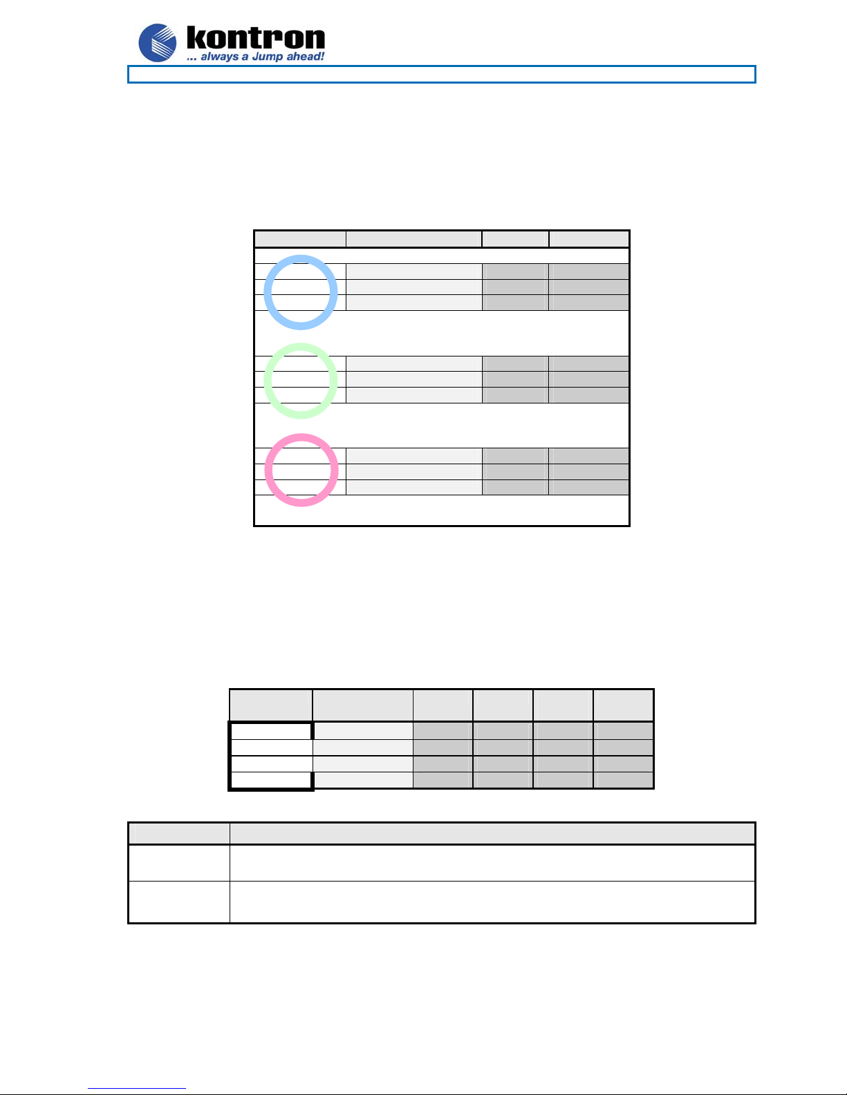
886LCD-M Family
KTD-00474-E Public User Manual Date: 2005-05-24 Page 43 of 78
4.11 Audio Connector
4.11.1 Audio Line-in, Line-out and Microphone
Audio Line-in, Line-out and Micro ph on e a re a vailable in the stacked audio jack connector.
IN Signal Type Note
TIP MIC 1 IA 1, 2
RING MIC 2 IA 1, 2
SLEEVE GND PWR 2
TIP Line out – Left OA
RING Line out – Right OA
SLEEVE GND PWR
TIP Line in – Left IA 1
RING Line in – Right IA 1
SLEEVE GND PWR
Note 1: Signals are shorted to GND intern ally in the connector, when jack-plug not inser te d.
Note 2: Microphone is not supported on En gineering board samples
4.11.2 CD-ROM Audio input (CDROM)
CD-ROM audio input may be connected to this connector. It may also be used as a secondary line-in signal.
PIN Signal Type Ioh/Iol Pull
1 CD_Left IA - -
2 CD_GND IA - -
3 CD_GND IA - -
4 CD_Right IA - -
Signal Description
CD_Left
CD_Right
CD_GND Analogue GND for Left and Right CD.
Left and right CD audio input lines or secondary Line-in.
(This analogue GND is not shorted to the general digital GND on the board).
U/D
Note
Page 44

886LCD-M Family
KTD-00474-E Public User Manual Date: 2005-05-24 Page 44 of 78
4.11.3 AUDIO Header (AUDIO_HEAD)
Pull
Note
AMP-LFE-OUT 1 2 AMP-CEN-OUT
AAGND 3 4 AAGND
SPKR_OUT_L 5 6 SPKR_OUT_R
AAGND 7 8 AAGND
SURR-OUT-L 9 10 SURR-OUT-R
VIDEO-L 11 12 VIDEO-R
AAGND 13 14 AAGND
F-FRONT-MIC1 15 16 F-FRONT-MIC2
AAGND 17 18 AAGND
F-AUX-IN-L 19 20 F-AUX-IN-R
F-MONO-OUT 21 22 AAGND
- - PWR GND 23 24 F-SPDIF-IN
F-SPDIF-OUT 25 26 GND PWR - -
Signal Description
AMP-LFE-OUT
AMP-CEN-OUT
SPKR_OUT_L
SPKR_OUT_R
SURR-OUT-L
SURR-OUT-R
VIDEO-L
VIDEO-R
F-FRONT-MIC1
F-FRONT-MIC2
F-AUX-IN-L
F-AUX-IN-R
F-MONO-OUT Speaker Phone Output
F-SPDIF-IN S/PDIF Input
F-SPDIF-OUT S/PDIF Output
AAGND Audio Analogue ground
U/D
Ioh/
Type Signal PIN Signal Type
Iol
Low Frequency Effect Out channel.
On 886LCD-M/ATX and M/Flex signal is amplified to 3W.
On 886LCD-M/mITX signal is un-amplified.
Center Out channel.
On 886LCD-M/ATX and M/Flex signal is amplified to 3W.
On 886LCD-M/mITX signal is un-amplified.
Speaker Out Left and Right Channel. Both signal are amplified to 3W.
Surround Out Left and Right chan ne l
Not connected
Dedicated MIC Input 1, 2 for Frontpan el MIC
AUX Left and Right Channel input
Ioh/
Iol
Pull
U/D
Note
Page 45

886LCD-M Family
KTD-00474-E Public User Manual Date: 2005-05-24 Page 45 of 78
4.12 Fan connectors , FAN_PROC and FAN_SYS.
The FAN_PROC is used for connection of the active cooler for the CPU.
The FAN_SYS can be used to power, control and monitor a fan for chassis ventilation etc.
PIN
1 SENSE PWR - 4K7
2 12V PWR - -
3 GND PWR - -
Signal description:
Signal Description
12V +12V supply for fan, can be turned on/off or modulated (PWM) by the chipset.
A maximum of 800 mA can be supplied from this pin.
SENSE Tacho signal from the fan for supervision. The signals shall be generated by an open
collector transistor or similar. On board is a pull-up resistor 4K7 to +12V. The signal has to be
pulses, typically 2 Hz per rotation.
Signal
Type Ioh/Iol
Pull
U/D
Note
4.13 The Clear CMOS Jumper, Clr-CMOS.
The Clr-CMOS Jumper is used to clear the CMOS content.
No Jumper installed 1 2 3 (Pin numbers)
Jumper normal position
Jumper in Clear CMOS position
To clear all CMOS settings, including Password protection, mov e the CMOS _CLR jumper (wit h or without
power on the system) for approximately 1 minute.
Alternatively if no jumper is available, turn off power and remove t he batt ery for 1 minu te, but be careful to
orientate the battery corretly whe n reinserted .
4.14 LPC connector (unsupported).
Pull
Note
U/D Ioh/Iol Type
- - PWR GND 1 2 LPCCLK
- - PWR GND 3 4 LPC AD0
LPC FRAME# 5 6 LPC AD1
INT SERIQ 7 8 LPC AD2
LPC DRQ#1 9 10 LPC AD3
Signal
↑ CPU location ↑
•
•
PIN
Signal
Type Ioh/Iol
Pull
U/D Note
Page 46

886LCD-M Family
KTD-00474-E Public User Manual Date: 2005-05-24 Page 46 of 78
4.15 Front Panel connector (FRONTPNL).
Pull
Note
U/D Ioh/Iol Type
USB13_5V 1 2 USB13_5V
USB1- 3 4 USB3-
USB1+ 5 6 USB3+
- - PWR GND 7 8 GND PWR - -
- - - NC 9 10 NC - - -
- - PWR +5V 11 12 +5V PWR - -
OC HD_LED 13 14 SUS_LED OC
- - PWR GND 15 16 PWRBTN_IN#
RSTIN# 17 18 GND PWR - -
SB3V3 19 20 NC - - -
AGND 21 22 AGND
SPKR_OUT_L 23 24 SPKR_OUT_R
Signal Description
+5V supply for the USB devices on USB Port 1 and 3 is on-board fused with a 1.5 A
USB13_5V
USB1+
USB1-
USB3+
USB3-
HD_LED Hard Disk Activity LED.
SUS_LED Suspend Mode LED
PWRBTN_IN# Power Button In. Toggle this signal low to start the ATX PSU and boot the board.
RSTIN# Reset Input. Pull low to reset the board.
SPKR_OUT_L Speaker Out Left channel, amplified, 3W
SPKR_OUT_R Speaker Out Right chann el, amplified, 3W
SB3V3 Standby 3.3V voltage
AGND Analogue Ground for Audio
reset-able fuse. The supply is common for the two channels. SB5V is supplied during
power down to allow wakeup on USB device activity.
Universal Serial Bus Port 1 Differentials: Bus Dat a/ Ad dress/ Command Bus.
Universal Serial Bus Port 3 Differentials: Bus Data/Address/Command Bus.
Signal
PIN
Signal
Type Ioh/Iol
Pull
U/D Note
4.16 Intruder Connector (INT)
This connector is available on the 886LCD-M/Flex only, however please noti ce that the INTRUDER function
is also available on the Feature connector.
PIN
1 GND PWR - -
2 INTRUDER# I - 100K
3 GND PWR - -
INTRUDER detect: May be used to detect if th e system case has been opened.
This signal’s status is readable, so it may be used li ke a G PI when the Intruder switch is not needed.
Signal
Type Ioh/Iol
Pull
U/D
Note
Page 47

886LCD-M Family
KTD-00474-E Public User Manual Date: 2005-05-24 Page 47 of 78
4.17 Feature Connector (FEATURE)
Pull
Note
Note 1: Pull-up to 3V3 supply
Note 2: Pull-up to RTC-Voltage
Note: For Engineering build, 26 pin header is mounted, causing INTRUDER#, GND, SMBC and SMBD
signals (pin 1, 2, 29, 30) to be unavailable .
INTRUDER#
EXT_ISAIRQ# EXTernal ISA IRQ, (active low input) can activate standard AT-Bus IRQ-interrupt.
U/D Ioh/Iol Type
2 100K/ - I INTRUDER# 1 2 GND PWR - -
EXT_ISAIRQ# 3 4 EXT_SMI# I
PWR_OK 5 6 SB5V PWR - -
- - PWR +3V3 7 8 EXT_BAT PWR - -
- - PWR +5V 9 10 GND PWR - -
IOT GPIO0 11 12 GPIO1 IOT
IOT GPIO2 13 14 GPIO3 IOT
IOT GPIO4 15 16 GPIO5 IOT
IOT GPIO6 17 18 GPIO7 IOT
- - PWR GND 19 20 FAN3OUT
FAN3IN 21 22 +12V PWR - -
TEMP3IN 23 24 VREF
- - PWR GND 25 26 IRRX
IRTX 27 28 GND PWR - -
1 2K7/ SMBC 29 30 SMBD 2K7/ 1
Signal Description
INTRUDER, may be used to detect if the system case has been opened. This signal’s
status is readable, so it may be used like a GPI whe n the Intruder switch is not needed.
EXT_SMI# External SMI, (active low input) signal can activate SMI interrupt.
PWR_OK PoWeR OK, signal is hi gh if no power failures is detected.
SB5V StandBy +5V supply.
+3V3
(EXTernal BATtery) the + terminal of an external primary cell battery can be connected
to this pin. The – terminal of the battery shall be connected to GND, for instance pin 10.
EXT_BAT
+5V
GPIO0..7
FAN3OUT FAN 3 speed control OUTput. This analogue voltage output controls the Fan’s speed.
FAN3IN FAN3 Input. 0V to +5V amplitude Fan 3 tachometer input.
+12V
TEMP3IN Temperature sensor 3 input.
VREF Voltage REFerence, reference voltage to be used with TEMP3IN input.
IRRX IR Receive input (IrDA 1.0, SIR up to 1.152K bps)
IRTX IR Transmit output (IrDA 1.0, SIR up to 1.152K bps)
SMBC SMBus Clock signal
SMBD SMBus Data signal
The on board battery circuit makes sure that the external battery will not be recharged.
The external battery can be used with or without the on board battery installed.
The external battery volta ge shall be in the range: 2.5 - 4.0 V DC.
General Purpose Inputs / Output. These Signals may be controlled or mon i t ored through
the use of the KONTRON API (Application Programming Interface) available for Win9 8,
WinXP, WinNT, and Win2000.
Signal
PIN
Signal
Type Ioh/Iol
Pull
U/D Note
Page 48
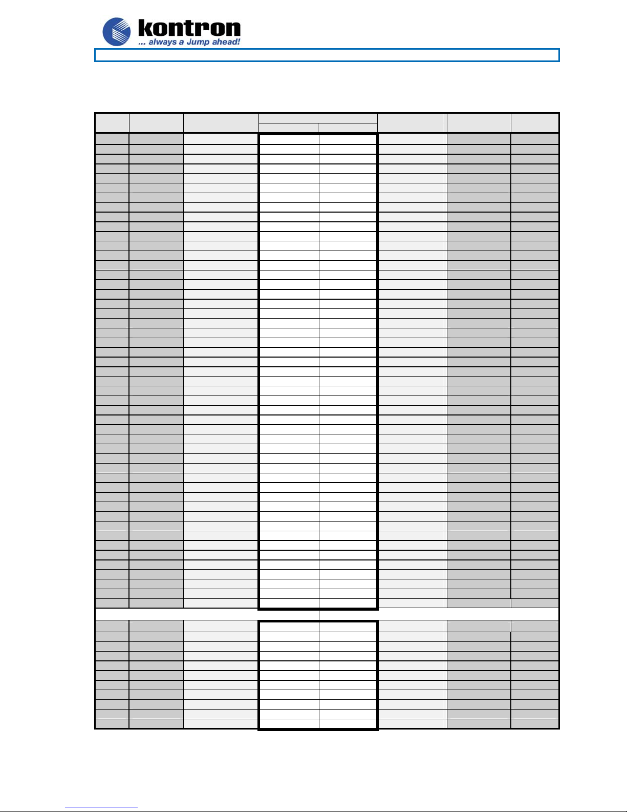
886LCD-M Family
KTD-00474-E Public User Manual Date: 2005-05-24 Page 48 of 78
4.17.1 PCI Slot Connector
Note Type Signal
PWR -12V F01 E01 TRST# O
O TCK F02 E02 +12V PWR
PWR GND F03 E03 TMS O
I TDO F04 E04 TDI O
PWR +5V F05 E05 +5V PWR
PWR +5V F06 E06 INTA# I
I INTB# F07 E07 INTC# I
I INTD# F08 E08 +5V PWR
I REQ2# F09 E09 CLKC O
I REQ3# F10 E10 +5V (I/O) PWR
OT GNT2# F11 E11 CLKD O
PWR GND F12 E12 GND PWR
PWR GND F13 E13 GND PWR
O CLKA F14 E14 GNT3# OT
PWR GND F15 E15 RST# O
O CLKB F16 E16 +5V (I/O) PWR
PWR GND F17 E17 GNT0# OT
I REQ0# F18 E18 GND PWR
PWR +5V (I/O) F19 E19 REQ1# I
IOT AD31 F20 E20 AD30 IOT
IOT AD29 F21 E21 +3.3V PWR
PWR GND F22 E22 AD28 IOT
IOT AD27 F23 E23 AD26 IOT
IOT AD25 F24 E24 GND PWR
PWR +3.3V F25 E25 AD24 IOT
IOT C/BE3# F26 E26 GNT1# OT
IOT AD23 F27 E27 +3.3V PWR
PWR GND F28 E28 AD22 IOT
IOT AD21 F29 E29 AD20 IOT
IOT AD19 F30 E30 GND PWR
PWR +3.3V F31 E31 AD18 IOT
IOT AD17 F32 E32 AD16 IOT
IOT C/BE2# F33 E33 +3.3V PWR
PWR GND F34 E34 FRAME# IOT
IOT IRDY# F35 E35 GND PWR
PWR +3.3V F36 E36 TRDY# IOT
IOT DEVSEL# F37 E37 GND PWR
PWR GND F38 E38 STOP# IOT
IOT LOCK# F39 E39 +3.3V PWR
IOT PERR# F40 E40 SDONE IO
PWR +3.3V F41 E41 SB0# IO
IOC SERR# F42 E42 GND PWR
PWR +3.3V F43 E43 PAR IOT
IOT C/BE1# F44 E44 AD15 IOT
IOT AD14 F45 E45 +3.3V PWR
PWR GND F46 E46 AD13 IOT
IOT AD12 F47 E47 AD11 IOT
IOT AD10 F48 E48 GND PWR
PWR GND F49 E49 AD09 IOT
SOLDER SIDE COMPONENT SIDE
IOT AD08 F52 E52 C/BE0# IOT
IOT AD07 F53 E53 +3.3V PWR
PWR +3.3V F54 E54 AD06 IOT
IOT AD05 F55 E55 AD04 IOT
IOT AD03 F56 F56 GND PWR
PWR GND F57 E57 AD02 IOT
IOT AD01 F58 E58 AD00 IOT
PWR +5V (I/O) F59 E59 +5V (I/O) PWR
IOT ACK64# F60 E60 REQ64# IOT
PWR +5V F61 E61 +5V PWR
PWR +5V F62 E62 +5V PWR
Terminal
S C
Signal Type Note
Page 49

886LCD-M Family
KTD-00474-E Public User Manual Date: 2005-05-24 Page 49 of 78
4.17.2 Signal Description –PCI Slot Connector
SYSTEM PINS
CLK
RST#
ADDRESS AND DATA
AD[31::00]
C/BE[3::0]#
PAR
INTERFACE CONTROL PINS
FRAME#
IRDY#
TRDY#
STOP#
LOCK#
IDSEL
DEVSEL#
Clock provides timing for all transactions on PCI and is an input to every PCI device. All other PCI signals,
except RST#, INTA#, INTB#, INTC#, and INT D#, are sam pled on the rising edge of CLK and all other
timing parameters are defined with respect to this edge. PCI operates at 33 MHz.
Reset is used to bring PCI-specific registers, sequencers, and signals to a consistent state. What effect
RST# has on a device beyond the PCI sequencer is beyond the scope of this specification, except for
reset states of required PCI configuration registers. Anytime RST# is asserted, all PCI output signals must
be driven to their benign state. In general, this means they must be asynchronously tri-stated. SERR#
(open drain) is floated. REQ# and GNT# must both be tri-stated (they cannot be driven low or high during
reset). To prevent AD, C/BE#, and PAR signals from floating during reset, the central resource may drive
these lines during reset (bus parking) but only to a logic low level–they may not be driven high.
RST# may be asynchronous to CLK when asserted or deasserted. Although asynchronous, deassertion is
guaranteed to be a clean, bounce-free edge. Except for configuration accesses, only devices that are
required to boot the system will respond after reset.
Address and Data are multiplexed on the same PCI pins. A bus transaction consists of an address phase
followed by one or more data phases. PCI supports both read and write bursts.
The address phase is the clock cycle in which FRAME# is asserted. During the address phase AD[31::00]
contain a physical address (32 bits). For I/O, this is a byte address; for configuration and memory, it is a
DWORD address. During data phases AD[07::00] contain the least significant byte (lsb) and AD[31::24]
contain the most significant byte (msb). Write data is stable and valid when IRDY# is asserted and read
data is stable and valid when TRDY# is asserted. Data is transferred during those clocks where both
IRDY# and TRDY# are asserted.
Bus Command and Byte Enables are multiplexed on the same PCI pins. During the address phase of a
transaction, C/BE[3::0]# define the bus command. During the data phase C/BE[3::0]# are used as Byte
Enables. The Byte Enables are valid for the entire data phase and determine which byte lanes carry
meaningful data. C/BE[0]# applies to byte 0 (lsb) and C/BE[3]# applies to byte 3 (msb).
Parity is even parity across AD[31::00] and C/BE[3::0]#. Parity generation is required by all PCI agents.
PAR is stable and valid one clock after the address phase. For data phases, PAR is stable and valid one
clock after either IRDY# is asserted on a write transaction or TRDY# is asserted on a read transaction.
Once PAR is valid, it remains valid until one clock after the completion of the current data phase. (PAR
has the same timing as AD[31::00], but it is delayed by one clock.) The master drives PAR for address and
write data phases; the target drives PAR for read data phases.
Cycle Frame is driven by the current master to indicate the beginning and duration of an access. FRAME#
is asserted to indicate a bus transaction is beginning. While FRAME# is asserted, data transfers contin ue.
When FRAME# is deasserted, the transaction is in the final data phase or has completed.
Initiator Ready indicates the initiating agent’s (bus master’s) ability to complete the current data phase of
the transaction. IRDY# is used in conjunction with TRDY#. A data phase is completed on any clock both
IRDY# and TRDY# are sampled asserted. During a write, IRDY# indicates that valid data is present on
AD[31::00]. During a read, it indicates the master is prepared to accept data. Wait cycles are inserted until
both IRDY# and TRDY# are asserted together.
Target Ready indicates the target agent’s (selected device’s) ability to complete the current data phase of
the transaction. TRDY# is used in conjunction with IRDY#. A data phase is completed on any clock both
TRDY# and IRDY# are sampled asserted. During a read, TRDY# indicates that valid data is present on
AD[31::00]. During a write, it indicates the target is prepared to accept data. Wait cycles are inserted until
both IRDY# and TRDY# are asserted together.
Stop indicates the current target is requesting the master to stop the current transaction.
Lock indicates an atomic operation that may require multiple transactions to complete. When LOCK# is
asserted, non-exclusive transactions may proceed to an address that is not currently locked. A grant to
start a transaction on PCI does not guarantee control of LOCK#. Control of LOCK# is obtained under its
own protocol in conjunction with GNT#. It is possible for different agents to use PCI while a single master
retains ownership of LOCK#. If a device implements Executable Memory, it should also implement LOCK#
and guarantee complete access exclusion in that memory. A target of an access that supports LOCK#
must provide exclusion to a minimum of 16 bytes (aligned). Host bridges that have system memory behind
them should implement LOCK# as a target from the PCI bus point of view and optionally as a master.
Initialization Device Select is used as a chip select during configuration read and write transactions.
Device Select, when actively driven, indicates the driving device has decoded its address as the target of
the current access. As an input, DEVSEL# indicates whether any device on the bus has been selected.
(continued)
Page 50
886LCD-M Family
KTD-00474-E Public User Manual Date: 2005-05-24 Page 50 of 78
ARBITRATION PINS (BUS MASTERS ONLY)
REQ#
GNT#
ERROR REPORTING PINS.
The error reporting pins are required by all devices and maybe asserted when enabled
PERR#
SERR#
INTERRUPT PINS (OPTIONAL).
Interrupts on PCI are optional and defined as “level sensitive,” asserted low (negative true), using open drain output
drivers. The assertion and deassertion of INTx# is asynchronous to CLK. A device asserts it s INTx# line when requesting
attention from its device driver. Once the INTx# signal is asserted, it remains asserted until the device driver clears the
pending request. When the request is cleared, the device deasserts its INTx# signal. PCI defines one interrupt line for a
single function device and up to four interrupt lines for a multi-function device or connector. For a single function device,
only INTA# may be used while the other three interrupt lines have no meaning.
INTA#
INTB#
INTC#
INTD#
Request indicates to the arbiter that this agent desires use of the bus. This is a point to point signal. Every
master has its own REQ# which must be tri-stated while RST# is asserted.
Grant indicates to the agent that access to the bus has been granted. This is a point to point signal. Every
master has its own GNT# which must be ignored while RST# is asserted.
While RST# is asserted, the arbiter must ignore all REQ# lines since they are tri-stated and do not contain
a valid request. The arbiter can only perform arbitration after RST# is deasserted. A master must ignor e its
GNT# while RST# is asserted. REQ# and GNT# are tri-state signals due to power sequencing
requirements when 3.3V or 5.0V only add-in boards are used with add-in boards that use a universal I/O
buffer.
Parity Error is only for the reporting of data parity errors during all PCI transactions except a Special Cycle.
The PERR# pin is sustained tri-state and must be driven active by the agent receiving data two clocks
following the data when a data parity error is detected. The minimum duration of PERR# is one clock for
each data phase that a data parity error is detected. (If sequential data phases each have a data parity
error, the PERR# signal will be asserted for more than a single clock.) PERR# must be driven high for one
clock before being tri-stated as with all sustained tri-state signals. There are no special conditions when a
data parity error may be lost or when reporting of an error may be delayed. An agent cannot report a
PERR# until it has claimed the access by asserting DEVSEL# (for a target) and completed a data phase
or is the master of the current transaction.
System Error is for reporting address parity errors, data parity errors on the Special Cycle command, or
any other system error where the result will be catastrophic. If an agent does not want a non-maskable
interrupt (NMI) to be generated, a different reporting mechanism is required. SERR# is pure open drain
and is actively driven for a single PCI clock by the agent reporting the error. The assertion of SERR# is
synchronous to the clock and meets the setup and hold times of all bused signals. However, the restoring
of SERR# to the deasserted state is accomplished by a weak pullup (same value as used for s/t/s) which
is provided by the system designer and not by the
take two to three clock periods to fully restore SERR#. The agent that reports SERR#s to the operating
system does so anytime SERR# is sampled asserted.
Interrupt A is used to request an interrupt.
Interrupt B is used to request an interrupt and only has meaning on a multi-function device.
Interrupt C is used to request an interrupt and only has meaning on a multi-function device.
Interrupt D is used to request an interrupt and only has meaning on a multi-function device.
ٛ signaling agent or central resource. This pull-up may
4.17.3 886LCD-M PCI IRQ & INT routing
Board type Slot IDSEL INTA INTB INTC INTD
886LCD-M/mITX
886LCD-M/FLEX
2 AD17 INT_PIRQ#F INT_PIRQ#G INT_PIRQ#H INT_PIRQ#E
3 AD18 INT_PIRQ#G INT_PIRQ#H INT_PIRQ#E INT_PIRQ#F
886LCD-M/ATX
2 AD17 INT_PIRQ#F INT_PIRQ#G INT_PIRQ#H INT_PIRQ#E
3 AD18 INT_PIRQ#G INT_PIRQ#H INT_PIRQ#E INT_PIRQ#F
4 AD19 INT_PIRQ#H INT_PIRQ#E INT_PIRQ#F INT_PIRQ#G
5 AD20 INT_PIRQ#D INT_PIRQ#C INT_PIRQ#B INT_PIRQ#A
6 AD21 INT_PIRQ#C INT_PIRQ#B INT_PIRQ#A INT_PIRQ#D
1 AD16 INT_PIRQ#E INT_PIRQ#F INT_PIRQ#G INT_PIRQ#H
1 AD16 INT_PIRQ#E INT_PIRQ#F INT_PIRQ#G INT_PIRQ#H
1 AD16 INT_PIRQ#E INT_PIRQ#F INT_PIRQ#G INT_PIRQ#H
Page 51

886LCD-M Family
KTD-00474-E Public User Manual Date: 2005-05-24 Page 51 of 78
5. Onboard Connectors
Connector Manufacturer Type no.
FAN_SYS, Molex 22-23-2031
FAN_PROC AMP 640456-3
INT
KBDMSE Molex 22-23-2061
AMP 640456-6
CDROM Foxconn HF11040
AMP 103669-3
Topyang 201904-013218N
SATA0 Molex 67491-0010
SATA1 Foxconn LD18071-S04
PWR12CON Molex 39-29-3046
Lotes Guangzhou ltd A7466SB5N
ATXPWR Molex 39-29-3206
FoxConn HM20100
COMB Foxconn HL20051
COMC Topyang 23010-2200001N
COMD
AUDIO_HEAD Foxconn HL54131
Molex 87331-2620
FRONTPNL Foxconn HL20121
Molex 70246-2421
Topyang 23024-2200001N
FEATURE Foxconn HL54151
Molex 87831-3020
Molex 87331-3020
LPC Tekcon 1136-A058-10S
Foxconn HC11051
IDE_P Foxconn HL20201-UD2
IDE_S
IDE_S2 Foxconn HS55227
LVDS Don Connex C44-40-B-G-1
Molex 87831-2620
Page 52
886LCD-M Family
KTD-00474-E Public User Manual Date: 2005-05-24 Page 52 of 78
6. System Ressources
6.1 Memory map
Address range (hex) Size Description
00000000- 0007FFFF 512 Kbytes Conventional memory
00080000- 0009FBFF 127 Kbyte Extended conventional memory
0009FC00- 0009FFFF 1 Kbyte Extended BIOS data
000A0000- 000AFFFF 64 Kbytes 885GME VGA Controller, Video memory and BIOS
000B0000- 000BFFFF 64 Kbytes 885GME VGA Controller, Video memory and BIOS
000C0000- 000CC5FF 49 Kbytes 885GME VGA Controller, Video memory and BIOS
000CC800- 000CD7FF 4 Kbytes Realtek 8169 Ethernet Controller
D0000000- DFFF F FFF 0xFFFFFFF 885GME Processor I/O Controlle r
E8000000- EFFFFFFF 0x7FFFFFF 885GME VGA Controller
F0000000- F7FFFFFF 0x7FFFFFF 885GME VGA Controller
FF7FF400- FF7FF4FF 0xFF Realtek 8169 Ethernet Controller
FF7FF800- FF7FF8FF 0xFF Realtek 8169 Ethernet Controller
FF7FFC00- FF7FFCFF 0xFF Realtek 8169 Ethernet Controller
FF980000- FF9FFFFF 0x7FFFF 885GME VGA Controller
FFA7B000- FFA7B00F 0xF PCI System Peripheral
FFA7B400- FFA7B7FF 0x3FF USB Controller
FFA7B800- FFA7B8FF 0xFF Realtek AC97 Audio
FFA7BC00- FFA7BDFF 0x1FF Realtek AC97 Audio
FFA7FC00- FFAFFFFF 0x803FF Ultra SATA Controller
FFA80000- FFAFFFFF 0x7FFFF 885GME VGA Controller
FFB00000- FFEFFFFF 0x3FFFFF Intel 82802 Firmware Hub Device
FFF00000- FFF FFFFF 1 Mbyte Intel 82802 Firmware Hub Device
6.2 PCI devices
Bus # Device # Function # Vendor ID Device ID IDSEL Chip Device Function
0 0 0 8086h 3580h AD11 6300ESB Host bridge
0 0 1 8086h 3584h 6300ESB I/O Controller
0 0 3 8086h 3585h 6300ESB I/O Controller
0 1 0 8086h 3581h AD12 6300ESB Pci to Pci bridge
0 2 0 8086h 3582h AD13 6300ESB VGA controller
0 2 1 8086h 3582h 6300ESB Display controller
0 28 0 8086h 25AEh AD39 6300ESB Pci to Pci bridge
0 29 0 8086h 25A9h AD40 6300ESB USB
0 29 1 8086h 25AAh 6300ESB USB
0 29 4 8086h 25ABh 6300ESB Watchdog timer
0 29 5 8086h 25ACh 6300ESB APIC
0 29 7 8086h 25ADh 6300ESB USB
0 30 0 8086h 244Eh AD41 6300ESB Pci to Pci bridge
0 31 0 8086h 25A1h AD42 6300ESB ISA Bridge
0 31 1 8086h 25A2h 6300ESB IDE Controller
0 31 2 8086h 25A3h 6300ESB IDE Controller
0 31 3 8086h 25A4h 6300ESB SMBus
0 31 5 8086h 25A6h 6300ESB Audio
0 * - - - * - PCI slot #1
0 * - - - * - PCI slot #2
0 * - - - * - PCI slot #3
0 * - - - * - PCI slot #4
2 1 0 10ECh 8169h AD12 RTL8110 Ethernet
2 2 0 10ECh 8169h AD13 RTL8110 Ethernet
2 3 0 10ECh 8169h AD14 RTL8110 Ethernet
* Values are dynamically selected in BIOS.
Note: All PCI slots for the 886LCD-M boards supports PCI BUS Mastering.
Page 53

886LCD-M Family
KTD-00474-E Public User Manual Date: 2005-05-24 Page 53 of 78
6.3 Interrupt Usage
Onboard system parity errors and IOCHCHK signal activation
Onboard Timer 0 Interrupt
Onboard Keyboard Interrupt
Used for Cascading IRQ8-IRQ15
May be used by onboard Serial Port A
May be used by onboard Serial Port B / IrDA Port
May be used by onboard Serial Port C
May be used by onboard Serial Port D
May be used by onboard SATA controller
May be used by onboard Parallel Port
May be used by onboard Floppy disk Controller
Used by onboard Real Time Clock Alarm
May be used by onboard P/S 2 support
Used for Onboard co-processor support
May be used by primary harddisk controller
May be used by secondary harddisk controller
May be used for onboard Sound System
May be used by onboard USB controller
May be used by onboard Ethernet controller 1
May be used by onboard Ethernet controller 2
May be used by onboard Ethernet controller 3
May be used by onboard VGA Controller
May be used by onboard SMBus Controller
IRQ
NMI
IRQ0
IRQ1
IRQ2
IRQ3
IRQ4
IRQ5
IRQ6
IRQ7
IRQ8
IRQ9
IRQ10
IRQ11
IRQ12
IRQ13
IRQ14
IRQ15
IRQ16
IRQ17
IRQ18
IRQ19
IRQ20
IRQ21
IRQ22
IRQ23
IRQ24
IRQ25
IRQ26
•
•
•
•
•
•
•
•
•
•
• •
•
•
•
•
•
•
•
•
• • • •
• • • •
• • • •
• • • •
• • • •
•
• • • •
•
Available on PCI slots as IRQA-IRQD depending on selections in the BIOS
Notes
•
•
•
•
•
•
•
•
•
•
•
•
3
3
3
3
3
3
3
3
3
3
3
1, 2
1, 2
1, 2
1, 2
1, 2
1, 2
1, 2
1, 2
1
1
1
Notes:
1. Availability of the shaded IRQs depends on the setting in the BIOS. According to the PCI Standard,
PCI Interrupts IRQA-IRQD can be shared.
2. These interrupt lines are managed by the PnP handler and are subject to change during system
initialisation.
3. IRQ16 to IRQ26 are APIC interrupts
Page 54

886LCD-M Family
KTD-00474-E Public User Manual Date: 2005-05-24 Page 54 of 78
6.4 I/O Map
Address (hex) Size Description
0020- 0021 1 Programmable interrupt controller
0040- 0043 4 System Timer
0060- 0060 1 Standard keyboard
0061- 0061 1 System speaker
0070- 0071 2 System CMOS/Real time clock
0170- 01F7 8 Secondary Parallel ATA IDE Channel
01F0- 01F7 8 Primary Parallel ATA IDE Channel
02E8- 02EF 8 Comport 4
02F8- 02FF 8 Comport 2
0378- 037F 8 Printer Port
03B0- 03BB 12 855GME VGA Controller
03C0- 03DF 32 855GME VGA Controller
03E8- 03EF 8 Comport 3
03F8- 03FF 8 Comport 1
0CF8- 0CFF 8 PCI Bus
D000- D0FF 256 Realtek 8169 Ethernet Controller
D000- DFFF 4096 PCI standard PCI-to-PCI brigde
D400- D4FF 256 Realtek 8169 Ethernet Controller
D800- D8FF 256 Realtek 8169 Ethernet Controller
E000- E01F 32 Standard Universal PCI to USB Host Controller
E080- E09F 32 Standard Universal PCI to USB Host Controller
E400- E41F 32 PCI System Management Bus
E480- E4BF 32 Realtek AC97 Audio
E800- E8FF 256 Realtek AC97 Audio
EC00- EC07 8 855GME VGA Controller
FC00- FC07 8 Primary Serial ATA IDE Channel
FC08- FC0F 8 Secondary Serial ATA IDE Chan ne l
6.5 DMA Channel Usage
DMA Channel Number Data Width System Ressources
0 8 or 16 bits Available
1 8 or 16 bits Available
2 8 or 16 bits Available
3 8 or 16 bits Available
4 8 or 16 bits DMA Controller
5 16 bits Available
6 16 bits Available
7 16 bits Available
Page 55

886LCD-M Family
KTD-00474-E Public User Manual Date: 2005-05-24 Page 55 of 78
7. Overview of BIOS features
This Manual section details specific BIOS features for the 886LCD-M boards.
The 886LCD-M boards are based on the AMI BIOS core version ?? with Kontron BIOS extensions.
7.1.1 System Management BIOS (SMBIOS / DMI)
SMBIOS is a Desktop Management Interf ace (DMI) compliant method for managing compu ters in a
managed network.
The main component of SMBIOS is the Management Informatio n Format (MIF) database, which contains
information about the computing system and its components. Using SMBIOS, a system administrator can
obtain the system types, capabili ties, operational status, and installat i on da te s for system components.
The MIF database defines the data and provides the method for accessing this inf or m at ion. The BIOS
enables applications such as third-part y m an ag ement software to use SMBIOS.
The BIOS stores and reports the followin g SMBIOS information:
• BIOS data, such as the BIOS revision level
• Fixed-system data, such as peripherals, serial numbers, and asset tags
• Resource data, such as memory size, cache size, and processor spe ed
• Dynamic data, such as event detection and error logging
Non-Plug and Play operating systems, such as Windows NT*, require an additional interface for obtaining
the SMBIOS information. The BIOS supports an SMBIOS table interface for such operating systems. Using
this support, an SMBIOS service-le vel application running on a non-Plug an d Play operating system can
obtain the SMBIOS information.
The 886LCD-M Boards supports reading certai n MIF specific details by the Windows API. Refer to the API
section in this manual for details.
7.1.2 Legacy USB Support
Legacy USB support enables USB devices such as keyboards, mice, and hubs to be used even when the
operating system’s USB drivers are not yet available. Legacy USB support is used to access the BIOS Setup
program, and to install an operating sy stem that supports USB. By default, Legacy USB support is set to
Enabled.
Legacy USB support operates as follows:
1. When you apply power to the computer, legacy support is disabled .
2. POST begins.
3. Legacy USB support is enabled by the BIOS allowing you to use a USB keyboard to enter and
configure the BIOS Setup prog ra m an d the maintenance menu.
4. POST completes.
5. The operating system loads. While the operating system is loading, USB keybo ar ds an d mice are
recognized and may be used to configure t h e op erating system. (Keyboards and mice are not
recognized during this period if Legacy USB support was set to Disabled in the BIOS Se tup
program.)
6. After the operating system loads the USB drivers, all legacy and non-legacy USB devices are
recognized by the operating system, and Legacy USB support from the BIOS is no longer used.
To install an operating system that supp orts USB, verify that Legacy USB sup po rt in th e BIOS Setup
program is set to Enabled and follow the operating system’s installation instructions.
Page 56

886LCD-M Family
KTD-00474-E Public User Manual Date: 2005-05-24 Page 56 of 78
8. BIOS Configuration / Setup
8.1 Introduction
The BIOS Setup is used to view and configure BIOS settings for the 886LCD-M board. The BIOS Setup is
accessed by pressing the DEL key after the Power-On Self-Test (POST) memory test begins and before the
operating system boot begins. T he Menu ba r look like this:
BIOS SETUP UTILITY
Main Advanced PCIPnP Boot Security Chipset Power Exit
The available keys for the Menu screens are a s:
Function Key Description
<←> or <→> Select Screen
<↑> or <↓> Select Item
<+> or <-> Change Field
<Tab> Select Field
<F1> General Help
<F10> Save and Exit
<Esc> Exits the Menu
8.2 Main Menu
Main Advanced PCIPnP Boot Security Chipset Power Exit
System Overview
AMIBIOS
Version : 08.00.10
Build Date: 004/26/05
ID : 886LCD18
PCB ID : 13
Serial # : 00333219
PCB ID : 53630100
Processor
Type : Intel(R) Pentium(R) M Processor 1500 MHz
Speed : 600MHz
System Memory
Size : 248MB
Speed : 266MHz
System Time [10:18:15]
System Date [Mon 04/28/2005]
V02.53 (C)Copyright 1985-2002, American Megatrends, Inc.
Main Menu Selections
You can make the following selections. Use the sub menus for other selections.
Feature Options Description
System Time HH:MM:SS Set the system time.
System Date MM/DD/YYYY Set the system date.
BIOS SETUP UTILITY
Use [ENTER], [TAB] or
[SHIFT-TAB] to select
a field.
Use [+] or [-] to
configure system Time.
<- Select Screen
|| Select Item
+- Change Field
Tab Select Field
F1 General Help
F10 Save and Exit
ESC Exit
Page 57

886LCD-M Family
KTD-00474-E Public User Manual Date: 2005-05-24 Page 57 of 78
8.3 Advanced Menu
BIOS SETUP UTILITY
Main Advanced PCIPnP Boot Security Chipset Power Exit
Advanced Settings
Warning: Setting wrong values in below sections
May cause system to malfunction.
>
CPU Configuration
>
IDE Configuration
>
LAN Configuration
>
Floppy Configuration
>
SuperIO Configuration
>
Hardware Health Configuration
>
Voltage Monitor
>
ACPI Configuration
>
Remote Access Configuration
>
USB Configuration
V02.53 (C)Copyright 1985-2002, American Megatrends, Inc.
Configure CPU.
<- Select Screen
|| Select Item
Enter Go to Sub Screen
F1 General Help
F10 Save and Exit
ESC Exit
8.3.1 Advanced settings – CPU Configuration
BIOS SETUP UTILITY
Advanced
Configure advanced CPU settings
Manufacturer: Intel
Brand String: Intel (R) Pentium(R) M processor 1500M
Frequency : 600MHz
FSB Speed : 400MHz
Cache L1 : 32 KB
Cache L2 : 1024 KB
Intel(R) SpeedStep(tm) tech. [Maximum Speed]
V02.53 (C)Copyright 1985-2002, American Megatrends, Inc.
Feature Options Description
Intel(R) SpeedStep(tm) tech.
Maximum Speed,
Minimum Speed,
Automatic,
Disabled
Select the operation mode of the CPU. To
ensure full performance of the CPU, use the
Maximum Speed setting.
Depending on AC or
Battery powered, CPU
speed will change
based on the
selections.
<- Select Screen
|| Select Item
+- Change Option
F1 General Help
F10 Save and Exit
ESC Exit
Page 58

KTD-00474-E Public User Manual Date: 2005-05-24 Page 58 of 78
8.3.2 Advanced settings – IDE Configuration
Main Advanced PCIPnP Boot Security Chipset Power Exit
IDE Configuration
IDE Configuration [P-ATA Only]
S-ATA Running Enhanced [Yes]
P-ATA Channel Selection [Both]
S-ATA Ports Definition [P0-3
Configure S-ATA as RAID [No]
Primary IDE Master : [Hard Disk]
Primary IDE Slave : [Not Detected]
Secondary IDE Master : [Not Detected]
Secondary IDE Slave : [Not Detected]
Third IDE Master : [Not Detected]
Third IDE Slave : [Not Detected]
Fourth IDE Master : [Not Detected]
Fourth IDE Slave : [Not Detected]
ATA(PI) 80Pin Cable Detection [Host & Device]
P-ATA1 Cable Detection force [Disabled]
P-ATA2 Cable Detection force [Disabled]
Hard Disk Write Protect [Disabled]
IDE Detect Time Out (Sec) [35]
V02.53 (C)Copyright 1985-2002, American Megatrends, Inc.
Feature Options Description
IDE Configuration
When P-ATA & S-ATA mode is selected:
Feature Options Description
Combined Mode Option P-ATA 1st Channe l,
S-ATA Ports Definition P0-Master/P1-Slave,
When S-ATA only mode is selected:
Feature Options Description
S-ATA Ports Definition P0-1st./P1-2nd.,
When P-ATA only mode is selected:
Feature Options Description
S-ATA Running Enhanced
Mode
P-ATA Channel Selection Primary,
S-ATA Ports Definition
Configure S-ATA as RAID
886LCD-M Family
BIOS SETUP UTILITY
Select IDE Mode.
P-ATA Only:
rd
./P1-4th]
Disable, P-ATA
Only, S-ATA Only,
Setup the configuration of the hard drive
interfaces
P-ATA & S-ATA
Setup the configuration of the hard drive
S-ATA 1st Channel
interfaces
Select physical ports (P0/P1) to be Master/Slave
P0-Slave/P1-Master
or Slave/Master
Select physical ports (P0/P1) to be 1st./2nd. or
P0-2nd./P1-1st.
2nd./1st.
Yes, No Setup the S-ATA interface to be running in
enhanced mode or legacy mode
Setup the active IDE channels
Secondary,
Both
rd
P0-3
th
P0-4
No, Yes
th
./P1-4
./P1-3rd
,
Select physical ports (P0/P1) to be 3
th/3rd
4
Only available when "P-ATA Only" is selected.
Note: Install the driver via USB-Floppy
connected to USB port 2 (lower conn.)
4 P-ATA & 2 S-ATA
S-ATA Only:
2 S-ATA
P-ATA & S-ATA
2 P-ATA & 2 S-ATA
<- Select Screen
|| Select Item
+- change option
F1 General Help
F10 Save and Exit
ESC Exit
rd/4th
or
Page 59

886LCD-M Family
KTD-00474-E Public User Manual Date: 2005-05-24 Page 59 of 78
Feature Options Description
ATA(PI) 80Pin Cable Detection
P-ATA1 Cable Detection Force
P-ATA2 Cable Detection Force
Hard Disk Write Protect
Host & Device,
Host,
Device
Disable, 40Pin, 80Pin
Disable, 40Pin, 80Pin
Disable, Enabled
Select the mechanism for detecting 80Pin
ATA Cable
Force the board to operate as if a 40P i n ATA
cable or 80Pin ATA cable is installed on the
Primary channel
Force the board to operate as if a 40P i n ATA
cable or 80Pin ATA cable is installed on the
Primary channel
Enable write protection on HDDs, only works
when it is accessed through the BIOS
IDE Detect Time Out (Sec)
Advanced
Primary IDE Master
Device :Hard Disk
Vendor :ST340014A
Size :40.0GB
LBA Mode :Supported
Block Mode :16Sectors
PIO Mode :4
Async DMA :MultiWord DMA-2
Ultra DMA :Ultra DMA-5
S.M.A.R.T. :Supported
Type [Auto]
LBA/Large Mode [Auto]
Block (Multi-Sector Transfer) [Auto]
PIO Mode [Auto]
DMA Mode [Auto]
S.M.A.R.T. [Auto]
32Bit Data Transfer [Auto]
0,5,10,15,20,25,30,35
BIOS SETUP UTILITY
Select the time out value when the BIOS is
detecting ATA/ATAPI Devices
Select the type of
devices connected to
the system
<- Select Screen
|| Select Item
+- Change Option
F1 General Help
F10 Save and Exit
ESC Exit
V02.53 (C)Copyright 1985-2002, American Megatrends, Inc.
Feature Options Description
Type
LBA/Large Mode
Block (Multi-Sector Transfer)
PIO Mode
Not Installed, Auto, CDROM,
ARMD
Disabled, Auto
Disabled, Auto
Auto, 0, 1, 2, 3, 4
Select the type of device installed
Enabling LBA causes Logical Block
Addressing to be used in place of
Cylinders, Heads, and Sectors.
Select if the device should run in Block
mode
Selects the method for transferring the
data between the hard disk and system
memory. The Setup menu only lists those
options supported by the drive and
platform.
(continued)
Page 60

886LCD-M Family
KTD-00474-E Public User Manual Date: 2005-05-24 Page 60 of 78
DMA Mode
S.M.A.R.T.
32Bit Data Transfer
Auto, SWDMA0, SWDMA1,
SWDMA2, MWDMA0,
MWDMA1, MWDMA2, UDMA0,
UDMA1, UDMA2, UDMA3,
UDMA4, UDMA5
Auto, Disabled, Enabled
Disabled, Enabled
8.3.3 Advanced settings – LAN Configuration
BIOS SETUP UTILITY
Main Advanced PCIPnP Boot Security Chipset Power Exit
Floppy Configuration
ETH1 Configuration [With PXE boot]
MAC Address : 00E0F4000001
ETH2 Configuration [Enabled]
MAC Address : 00E0F4000002
ETH3 Configuration [Enabled]
MAC Address : 00E0F4000003
V02.53 (C)Copyright 1985-2002, American Megatrends, Inc.
Feature Options Description
ETH1 Configuration
ETH2 Configuration
ETH3 Configuration
Disabled, Enabled,
With RPL/PXE boot
Disabled, Enabled,
With RPL/PXE boot
Disabled, Enabled,
With RPL/PXE boot
Selects the Ultra DMA mode used for
moving data to/from the drive. Autotype
the drive to select the optimum transfer
mode. Note : To use UDMA Mode 2, 3,
4 and 5 with a device, the harddisk
cable used MUST be UDMA66/100/133
cable (80 conductor cable).
Select if the Device should be monitoring
itself ( Self-Monitoring, Analysis and
Reporting Technology System)
Select if the Device should be using
32Bit data Transfer
Select the type of
floppy drive connected
to the system
<- Select Screen
|| Select Item
+- change option
F1 General Help
F10 Save and Exit
ESC Exit
Select if you want to enable the LAN
adapter, or if you want to activate the
RPL/PXE boot rom
Select if you want to enable the LAN
adapter, or if you want to activate the
RPL/PXE boot rom
Select if you want to enable the LAN
adapter, or if you want to activate the
RPL/PXE boot rom
Page 61

886LCD-M Family
KTD-00474-E Public User Manual Date: 2005-05-24 Page 61 of 78
8.3.4 Advanced settings – Floppy Configuration
BIOS SETUP UTILITY
Main Advanced PCIPnP Boot Security Chipset Power Exit
Floppy Configuration
Floppy A [Disabled]
Floppy B [Disabled]
V02.53 (C)Copyright 1985-2002, American Megatrends, Inc.
Feature Options Description
Floppy A
Floppy B
Disabled,
360KB, 1.2MB,
720KB, 1.44MB,
2.88MB
Disabled,
360KB, 1.2MB,
720KB, 1.44MB,
2.88MB
Select Floppy device installed in the sy stem using the
LPT->Floppy cable
Select Floppy device installed in the sy stem using the
LPT->Floppy cable
Select the type of
floppy drive connected
to the system
<- Select Screen
|| Select Item
+- change option
F1 General Help
F10 Save and Exit
ESC Exit
Page 62

886LCD-M Family
KTD-00474-E Public User Manual Date: 2005-05-24 Page 62 of 78
8.3.5 Advanced settings – SuperIO Configuration
BIOS SETUP UTILITY
Main Advanced PCIPnP Boot Security Chipset Power Exit
Configure Win627THF Super IO Chipset
OnBoard Floppy Controller [Disabled]
Serial Port1 Address [3F8/IRQ4]
Serial Port2 Address [2F8/IRQ3]
Serial Port2 Mode [Normal]
Parallel Port Mode [378]
Parallel Port Mode [Normal]
Parallel Port IRQ [IRQ7]
ICH SIO Serial Port1 Addresse [Disabled]
ICH SIO Serial Port2 Addresse [Disabled]
V02.53 (C)Copyright 1985-2002, American Megatrends, Inc.
Feature Options Description
OnBoard Floppy Controller
Serial Port1 Address
Serial Port2 Address Disabled, 3F8/IRQ4,
Serial Port2 Mode
Parallel Port Address
Parallel Port Mode Normal, Bi-Directional,
EPP Version 1.9, 1.7 Setup with version of EPP you want to run
ECP Mode DMA Channel DMA0, DMA1, DMA3 Select a DMA channel
Parallel Port IRQ IRQ5, IRQ7 Select a IRQ
ICH SIO Serial Port1 Address
ICH SIO Serial Port2 Address
Disabled, Enabled
Disabled, 3F8/IRQ4,
2F8/IRQ3, 3E8/IRQ4,
2E8/IRQ3, 3E8/IRQ6,
3E8/IRQ10, 2E8/IRQ11
2F8/IRQ3, 3E8/IRQ4,
2E8/IRQ3, 3E8/IRQ6,
3E8/IRQ10, 2E8/IRQ11
Normal,IRDA,ASK IR
Disabled, 378, 278, 3BC
EPP, ECP
Disabled, 3F8/IRQ4,
2F8/IRQ3, 3E8/IRQ4,
2E8/IRQ3, 3E8/IRQ6,
3E8/IRQ10, 2E8/IRQ11
Disabled, 3F8/IRQ4,
2F8/IRQ3, 3E8/IRQ4,
2E8/IRQ3, 3E8/IRQ6,
3E8/IRQ10, 2E8/IRQ11
Enable or disable the Floppy Controller
Select the BASE I/O addresse and IRQ
Select the BASE I/O addresse and IRQ
Select Mode for Serial Port2
Select the I/O address for the LPT.
NOTE: you cannot enable the floppy
controller and parallel port at the same
time!
Select the mode that the parallel port will
operate in
on the parallel port
Select the BASE I/O addresse and IRQ
Select the BASE I/O addresse and IRQ
Enable onboard Floppy
Controller for use at
parallel port
<- Select Screen
|| Select Item
+- change option
F1 General Help
F10 Save and Exit
ESC Exit
Page 63

886LCD-M Family
KTD-00474-E Public User Manual Date: 2005-05-24 Page 63 of 78
8.3.6 Advanced settings – Hardware Health Configuration
BIOS SETUP UTILITY
Main Advanced PCIPnP Boot Security Chipset Power Exit
Hardware Health Event Monitoring
System Temperature :37ºC/98ºF
CPU Temperature :43ºC/109ºF
External Temperature Sensor :N/A
Fan1 Speed :Fail
Fan Cruise Control [Disabled]
Fan2 Speed :2537 RPM
Fan Cruise Control [Thermal]
Fan Setting [45°C/113°F]
Fan3 Speed :2164
Fan Cruise Control [Speed]
Fan Setting [2177 RPM]
V02.53 (C)Copyright 1985-2002, American Megatrends, Inc.
Feature Options Description
Fan Cruise Control
Fan Settings 1406-5625 RPM,
Main Advanced PCIPnP Boot Security Chipset Power Exit
Voltage Monitor
Requested Core :1.484 V
VcoreA :1.431 V
VcoreB :1.483 V
+3.3Vin :3.290 V
+5Vin :4.985 V
+12Vin :12.016 V
-12Vin :Good
+5VSB :5.012 V
V02.53 (C)Copyright 1985-2002, American Megatrends, Inc.
Disabled, Thermal, Speed
30°-75°C
BIOS SETUP UTILITY
Select how the Fan shall operate.
When set to Thermal, the Fan will start to run at
the CPU die temperature set below.
When set to Speed, the Fan will run at the Fixed
speed set below.
The fan can operate in Thermal mode or in a
fixed fan speed mode
Enable Hardware Health
Monitoring Device.
<- Select Screen
|| Select Item
+- change option
F1 General Help
F10 Save and Exit
ESC Exit
Enable Hardware Health
Monitoring Device.
<- Select Screen
|| Select Item
+- change option
F1 General Help
F10 Save and Exit
ESC Exit
Page 64
886LCD-M Family
KTD-00474-E Public User Manual Date: 2005-05-24 Page 64 of 78
8.3.7 Advanced settings – ACPI Configuration
BIOS SETUP UTILITY
Main Advanced PCIPnP Boot Security Chipset Power Exit
ACPU Settings
ACPI Aware O/S [Yes]
>
General ACPI Configuration
>
Advanced ACPI Configuration
V02.53 (C)Copyright 1985-2002, American Megatrends, Inc.
Feature Options Description
ACPI Aware O/S
No, Yes
Select if your O/S supports ACPI
Enable Hardware Health
Monitoring Device.
<- Select Screen
|| Select Item
+- change option
F1 General Help
F10 Save and Exit
ESC Exit
8.3.8 Advanced settings – General ACPI Configuration
BIOS SETUP UTILITY
Main Advanced PCIPnP Boot Security Chipset Power Exit
Genral ACPI Configuration
Suspend mode [S1 & S3 (STR)]
Repost Video on S3 Resume [No]
S4BIOS Support [Disabled]
V02.53 (C)Copyright 1985-2002, American Megatrends, Inc.
Feature Options Description
Suspend mode
Repost Video on S3
Resume
S4BIOS Support
S1 (POS) only, S1&S3 (STR)
No, Yes
Disabled, Enabled
Select the ACPI state used for System Suspend
Determines whether to invoke VGA BIOS post on
S3/STR resume
Determines if you want to support S4 power state
Select the ACPI state
used for System
Suspend.
<- Select Screen
|| Select Item
+- change option
F1 General Help
F10 Save and Exit
ESC Exit
Page 65

886LCD-M Family
KTD-00474-E Public User Manual Date: 2005-05-24 Page 65 of 78
8.3.9 Advanced settings – Advanced ACPI Configuration
BIOS SETUP UTILITY
Main Advanced PCIPnP Boot Security Chipset Power Exit
Advanced ACPI Configuration
ACPI 2.0 Features [No]
ACPI APIC support [Enabled]
APIC ACPI SCI IRQ [Disabled]
AMI OEMB table [Enabled]
Headless mode [Disabled]
V02.53 (C)Copyright 1985-2002, American Megatrends, Inc.
Feature Options Description
ACPI 2.0 Features
ACPI APIC support
APIC ACPI SCI IRQ
AMI OEMB table
Headless mode
No, Yes
Enabled, Disabled
Enabled, Disabled
Enabled, Disabled
Enabled, Disabled
Enable/ Disable ACPI 2.0 features
Setup if the APIC controller should be supported
in the ACPI code
Enable/ Disable APIC ACPI SCI IRQ
Enable/ Disable AMI OEMB table
Enable/ Disable Headless mode
Enable RSDP pointers
to 64-bit Fixed System
Description Tables.
<- Select Screen
|| Select Item
+- change option
F1 General Help
F10 Save and Exit
ESC Exit
8.3.10 Advanced settings – Remote Access Configuration
BIOS SETUP UTILITY
Main Advanced PCIPnP Boot Security Chipset Power Exit
Configure Remote Access type and parameters
Remote Access [Enabled]
Serial port number [ICH COM1]
Serial Port Mode [115200 8,n,1]
Flow Control [None]
Redirection [Always]
Terminal Type [ANSI]
VT-UTF8 Combo Key Support [Disabled]
V02.53 (C)Copyright 1985-2002, American Megatrends, Inc.
Enable RSDP pointers
to 64-bit Fixed System
Description Tables.
<- Select Screen
|| Select Item
+- change option
F1 General Help
F10 Save and Exit
ESC Exit
Page 66
886LCD-M Family
KTD-00474-E Public User Manual Date: 2005-05-24 Page 66 of 78
Feature Options Description
Remote Access
Serial port number SIO COMA, SIO
Serial Port Mode 115200 8 n 1,
Flow Control None, Hardware,
Redirection After BIOS POST Disabled, Boot Loader,
Terminal Type ANSI, VT100, VT- UTF8 Select the target terminal type
VT-UTF8 Combo Key Support Disabled, Enabled Setup VT-UTF8 Combo Ke y
Disabled, Enabled
COMB, ICH COM1,
ICH COM2
57600 8 n 1,
38400 8 n 1,
19200 8 n 1,
09600 8 n 1
Software
Always
Allows you to see the screen over the
comport interface, in a terminal window
Setup which comport that should be used for
communication
Select the serial port speed
Select Flow Control for serial port
How long shall the BIOS send the picture
over the serial port
8.3.11 Advanced settings – USB Configuration
BIOS SETUP UTILITY
Main Advanced PCIPnP Boot Security Chipset Power Exit
USB Configuration
Module Version – 2.24.0-7.4
USB Devices Enabled :
1 Drive
USB Function [All USB Ports]
Legacy USB Support [Enabled]
USB 2.0 Controller [Enabled]
USB 2.0 Controller Mode [HiSpeed]
>
USB Mass Storage Device Configuration
V02.53 (C)Copyright 1985-2002, American Megatrends, Inc.
Feature Options Description
USB Function
Legacy USB Support
USB 2.0 Controller
USB 2.0 Controller Mode
Disabled, 2 USB Ports, All
USB Ports
Disabled, Enabled, Auto
Enabled, Disabled
FullSpeed, HiSpeed
Select the USB ports you want to enabled
Support for legacy USB Keyboard
Setup the USB 2 controller (480Mbps)
Configures the USB 2.0 controller in HiSpeed
(480Mbps) or FullSpeed (12Mbps)
Enables USB host
controllers.
<- Select Screen
|| Select Item
+- change option
F1 General Help
F10 Save and Exit
ESC Exit
Page 67

886LCD-M Family
KTD-00474-E Public User Manual Date: 2005-05-24 Page 67 of 78
8.3.12 Advanced settings – USB Mass Storage Device Configuration
BIOS SETUP UTILITY
Main Advanced PCIPnP Boot Security Chipset Power Exit
USB Mass Storage Device Configuration
USB Mass Storage Reset Delay [20 Sec]
Device #1 JetFlash TS256MJF2L
Emulation Type [Auto]
V02.53 (C)Copyright 1985-2002, American Megatrends, Inc.
Feature Options Description
USB Mass Storage Reset Delay
Emulation Type
10 Sec, 20 Sec, 30
Sec, 40 Sec
Auto, Floppy, Forced
FDD, Hard Disk,
CDROM
Number of seconds the BIOS waits for the
USB device after start unit command
Setup the emulation type for the USB device
Enables USB host
controllers.
<- Select Screen
|| Select Item
+- change option
F1 General Help
F10 Save and Exit
ESC Exit
Page 68

886LCD-M Family
KTD-00474-E Public User Manual Date: 2005-05-24 Page 68 of 78
8.4 PCIPnP Menu
BIOS SETUP UTILITY
Main Advanced PCIPnP Boot Security Chipset Power Exit
Advanced PCI/PnP Settings
Warning: Setting wrong values in below sections
May cause system to malfunction.
Plug & Play O/S [No]
PCI Latency Timer [64]
Allocate IRQ to PCI VGA [Yes]
PCI IDE BusMaster [Enabled]
PCI Raiser Support [Disabled]
Disable Unsed PCI Clocks [Auto]
Spread Spectrum Mode [Disabled]
V02.53 (C)Copyright 1985-2002, American Megatrends, Inc.
Feature Options Description
Plug & Play O/S
PCI Latency Timer
Allocate IRQ to PCI VGA
PCI IDE BusMaster
PCI Raiser Support
Disable Unused PCI Clocks
Spread Spectrum
No, Yes
32, 64, 96, 128, 160,
192, 224, 248
Yes, No
Enabled, Disabled
Disabled, PCI Slot3,
PCI Slot2, PCI Slot1
Auto, No
Disabled, Enabled
Select if you have a PnP O/S
Value in units of PCI clocks for PCI device
latency timer register
Assigns IRQ to PCI VGA card
Setup PCI bus mastering for read/write to IDE
drives
Setup if you are using a PCI Raiser card to
get one more PCI Slot (Vertical)
Disables PCI clocks if no PCI card is
detected
A technique for spreading the signal
bandwidth over a wide range of freque ncies
to lower Radiated Emission
NO: lets the BIOS
configure all the
devices in the system.
YES: lets the
operating system
configure Plug and
Play (PnP) devices not
required for boot if
your system has a Plug
and Play operating
system.
<- Select Screen
|| Select Item
+- change option
F1 General Help
F10 Save and Exit
ESC Exit
Page 69

886LCD-M Family
KTD-00474-E Public User Manual Date: 2005-05-24 Page 69 of 78
8.5 Boot Menu
BIOS SETUP UTILITY
Main Advanced PCIPnP Boot Security Chipset Power Exit
Boot Settings
>
Boot Settings Configuration
>
Boot Device Priority
Removable Devices 1st [No]
V02.53 (C)Copyright 1985-2002, American Megatrends, Inc.
Feature Options Description
Removable Devices 1st
No, Yes
Should removable USB devices get first boot
priority when inserted
Configure Settings
during System Boot.
<- Select Screen
|| Select Item
Enter Go to Sub Screen
F1 General Help
F10 Save and Exit
ESC Exit
8.5.1 Boot – Boot Settings Configuration
BIOS SETUP UTILITY
Main Advanced PCIPnP Boot Security Chipset Power Exit
Boot Settings
Quick Boot [Enabled]
Quiet Boot [Disabled]
Bootup Num-Lock [On]
PS/2 Mouse Support [Auto]
Halt on [All, But Keyboard]
Hit ‘DEL’ Message Display [Enabled]
Interrupt 19 Capture [Disabled]
V02.53 (C)Copyright 1985-2002, American Megatrends, Inc.
Configure Settings
during System Boot.
<- Select Screen
|| Select Item
Enter Go to Sub Screen
F1 General Help
F10 Save and Exit
ESC Exit
Page 70
886LCD-M Family
KTD-00474-E Public User Manual Date: 2005-05-24 Page 70 of 78
Feature Options Description
Quick Boot
Quiet Boot
Bootup Num-Lock
PS/2 Mouse Support
Halt on
Hit ‘DEL’ Message Display
Interrupt 19 Capture
Enabled, Disabled
Disabled, Enabled,
Enabled & Maintain
Off, On
Disabled, Enabled, Auto
Disabled, All But
Keyboard
Disabled, Enabled
Disabled, Enabled
8.6 Security Menu
BIOS SETUP UTILITY
Main Advanced PCIPnP Boot Security Chipset Power Exit
Security Settings
Supervisor Password :Installed
User Password :Installed
Change Supervisor Password
User Access Level [Full Access]
Change User Password
Clear User Password
Password Check [Setup]
Boot Sector Virus Protection [Disabled]
Hard Disk Security
Primary Master HDD User Password
Primary Slave HDD User Password
Secondary Slave HDD User Password
V02.53 (C)Copyright 1985-2002, American Megatrends, Inc.
Feature Options Description
Change Supervisor Passw ord Passwor d Change the Supervisor Password
User Access Level No Access, View Only,
Limited, Full Access
Change User Password Password Change th e Use r Pa ssword
Clear User Password Ok, Cancel Clears the User Password
Password Check Setup, Always Shall the BIOS prompt for password on bo ot or
Boot Sector Virus Protection
HDD Password Password Locks the HDD with a p asswo rd, the user
Enabled, Disabled
Allows BIOS to skip certain test while booting
Shows boot logo instead of POST screen
Select Power-on state for numlock
Select support for PS/2 Mouse
Wait for F1 key to be pressed if error. If no
keyboard present post will continue
Display the message or not
Allows option ROMs to trap interrupt 19
Install or Change the
password.
<- Select Screen
|| Select Item
Enter Go to Sub Screen
F1 General Help
F10 Save and Exit
ESC Exit
Set the user level Access for the BIOS
only when entering setup
Will write protect the MBR when the BIOS is
used to access the harddrive
needs to type the password on po wer on
Page 71

886LCD-M Family
KTD-00474-E Public User Manual Date: 2005-05-24 Page 71 of 78
8.7 Chipset Menu
BIOS SETUP UTILITY
Main Advanced PCIPnP Boot Security Chipset Power Exit
Advanced Chipset Settings
Warning: Setting wrong values in below sections may
cause system to malfunction.
>
Intel Montara-GML NorthBridge Configuration
>
SouthBridge Configuration
V02.53 (C)Copyright 1985-2002, American Megatrends, Inc.
Intel Montara-GML
NorthBridge chipset
configuration options.
<- Select Screen
|| Select Item
Enter Go to Sub Screen
F1 General Help
F10 Save and Exit
ESC Exit
Page 72

886LCD-M Family
KTD-00474-E Public User Manual Date: 2005-05-24 Page 72 of 78
8.7.1 Advanced Chipset Settings – Intel Montara-GML NorthBridge Configuration
BIOS SETUP UTILITY
Main Advanced PCIPnP Boot Security Chipset Power Exit
Configure advanced settings for NorthBrigde
Primary Video Device [Auto]
Graphics Mode Select [Enabled, 8MB]
IGD – Device 2,Function 1: [Enabled]
Boot Type: [CRT]
Backlight Signal inversion [Enabled]
LCDVCC Voltage [3.3V]
LVDS [Normal]
DVO [N/A]
V02.53 (C)Copyright 1985-2002, American Megatrends, Inc.
Feature Options Description
Primary Video Device Internal, External PCI,
External AGP, Auto
Graphics Mode Select Disabled, 1MB, 4MB,
8MB, 16MB, 32MB
IGD – Device 2, Function 1
Boot Type
Backlight Signal Inversion
LCDVCC Voltage
LVDS Panels Chose the connected LVDS panel
DVO DVO Chip Select the DVO connection
Disabled, Enabled
VBIOS Default, CRT,
LFP, CRT+LFP, EFP,
TV, CRT+EFP,
CRT+TV, EFP+EFP2,
EFP+TV
Disabled, Enabled
3.3V, 5V
Select witch graphics controller to use a s th e
primary boot device
Select the amount of system memory used by
the internal graphics device
Setup the multimonitor function
Setup type of boot screen
Select the signal polarity
Setup the LCD Voltage
Select which graphics
controller to use as
the primary boot
device.
<- Select Screen
|| Select Item
Enter Go to Sub Screen
F1 General Help
F10 Save and Exit
ESC Exit
Page 73

886LCD-M Family
KTD-00474-E Public User Manual Date: 2005-05-24 Page 73 of 78
8.7.2 Advanced Chipset Settings – SouthBridge Configuration
BIOS SETUP UTILITY
Main Advanced PCIPnP Boot Security Chipset Power Exit
IOAPIC [Enabled]
Extended IOAPIC [Enabled]
OnBoard AC’97 Audio [Enabled]
OnBoard Amplifier [Enabled]
V02.53 (C)Copyright 1985-2002, American Megatrends, Inc.
Feature Options Description
IOAPIC
Extended IOAPIC
OnBoard AC’97 Audio
OnBoard Amplifier
Disabled, Enabled
Disabled, Enabled
Disabled, Enabled
Disabled, Enabled
Setup the ICHS IOAPIC function
Setup the extended mode of I CHS I O APIC
Setup the onboard audio
Use the OnBoard Amplifier on lineout
Enable / Disable the
ICH4 IOAPIC function.
<- Select Screen
|| Select Item
Enter Go to Sub Screen
F1 General Help
F10 Save and Exit
ESC Exit
Page 74
886LCD-M Family
KTD-00474-E Public User Manual Date: 2005-05-24 Page 74 of 78
8.8 Power Menu
BIOS SETUP UTILITY
Main Advanced PCIPnP Boot Security Chipset Power Exit
ADVANCED SMI ENABLE CONTROLS
Power Management/APM [Enabled]
Power Button Mode [On/Off]
ADVANCED RESUME EVENT CONTROLS
USB Controller Resume [Enabled]
PME Resume [Disabled]
RI Resume [Disabled]
RTC Resume [Enabled]
RTC Alarm Data [11]
RTC Alarm Time [11:11:11]
PS/2 Kbd/Mouse S4/S5 Wake [Disabled]
S3-S5 Keyboard Hotkey [Any key]
AC Power Loss Restart [Off]
V02.53 (C)Copyright 1985-2002, American Megatrends, Inc.
Feature Options Description
Power Management/APM
Power Button Mode
USB Controller Resume
PME/WOL
RI Resume
RTC Resume
RTC Alarm Date Every Day, 1-31 Setup the date you want the board to start
RTC Alarm Time HH:MM:SS Setup the time you want t h e bo ar d to start
PS/2 Kbd/Mouse S4/S5
Wake
S3-S5 Keyboard Hotkey
AC Power Loss Restart
Disabled, Enabled
On/Off, Suspend
Disabled, Enabled
Disabled, Enabled
Disabled, Enabled
Enabled, Disabled
Disabled, Enabled
Any key, Space, Enter,
Sleep button
Off, On, Previous State
Setup the SMI/APM support
Select Power button functionality
Lets the USB devices wake up from sleep state
Allow PME/WOL to wake from sleep states
Allow RI/Modem to wake from sleep st at es
Let the board start up on a specific date and
time
When disabled the board can wake from S1
and S3, and when enabled it can also wake
from S4 and S5
Setup the key that can wake up the board
Select whether or not to restart th e sy stem after
AC power loss:
Off keeps the power off until the power button
is pressed.
On restores power to the compute r.
Previous State restores the previous power
state before power loss occurred.
Enable/Disable SMI
based power management
and APM support.
<- Select Screen
|| Select Item
+- Change Option
F1 General Help
F10 Save and Exit
ESC Exit
Page 75
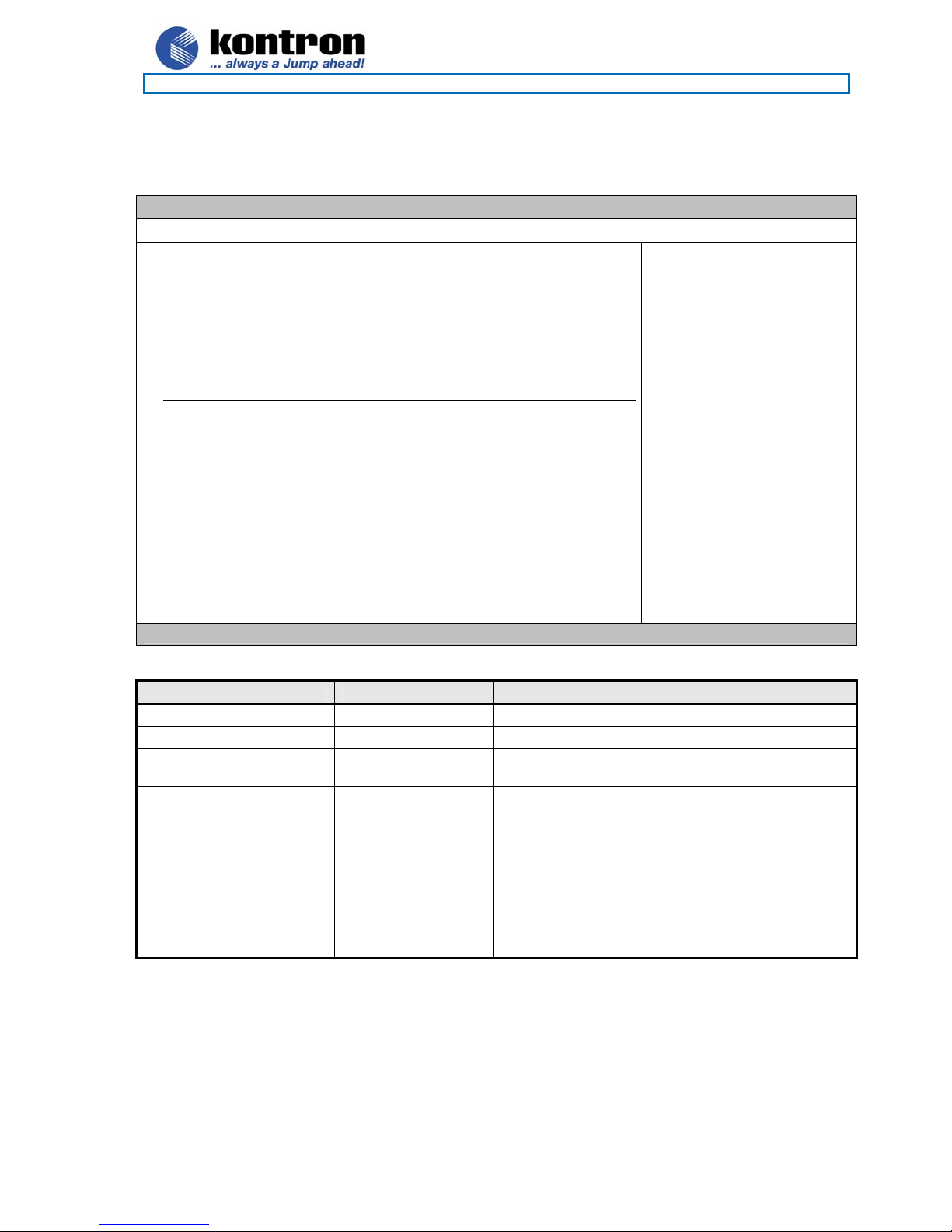
886LCD-M Family
KTD-00474-E Public User Manual Date: 2005-05-24 Page 75 of 78
8.9 Exit Menu
BIOS SETUP UTILITY
Main Advanced PCIPnP Boot Security Chipset Power Exit
Exit Options
Save Changes and Exit
Discard Changes and Exit
Discard Changes
Load Optimal Defaults
Load Failsafe Defaults
Halt on invalid Time/Date [Enabled]
Secure CMOS [Disabled]
V02.53 (C)Copyright 1985-2002, American Megatrends, Inc.
Feature Options Description
Save Changes and Exit Ok, Cancel Exit system setup after saving the changes
Discard Changes and Exit Ok, Cancel Exit system setup without saving any changes
Discard Changes Ok, Can cel Discards changes done so far to any of the setup
questions
Load Optimal Defaults Ok, Cancel Load Optimal Default values for all the setup
questions
Load Failsafe Defaults Ok, Cancel Load Failsafe Default values for al l the setup
questions
Halt on invalid Time/Date
Secure CMOS
Enabled, Disabled
Disabled, Enabled
Shall the BIOS halt and wait for a keypress when the
cmos is corrupted
Enable will store the current CMOS in the BIOS flash
rom, this will maintain the settings even if the battery
is failing
Exit system setup
after saving the
changes.
F10 Key can be used
for this operation.
<- Select Screen
|| Select Item
Enter Go to Sub Screen
F1 General Help
F10 Save and Exit
ESC Exit
Page 76

886LCD-M Family
KTD-00474-E Public User Manual Date: 2005-05-24 Page 76 of 78
8.10 AMI BIOS Beep Codes
Boot Block Beep Codes:
Number of
Beeps
1 Insert diskette in floppy drive A:
2 ‘AMIBOOT.ROM’ file not found in root directory of diske tte in A:
3 Base Memory error
4 Flash Programming successful
5 Floppy read error
6 Keyboard controller BAT command failed
7 No Flash EPROM de tected
8 Floppy controller failure
9 Boot Block BIOS checksum error
10 Flash Erase error
11 Flash Program error
12 ‘AMIBOOT.ROM’ file size error
13 BIOS ROM image mismatch (file lay out does not match image present in flash dev ice )
Description
POST BIOS Beep Codes:
Number of
Beeps
1 Memory refresh timer error.
2 Parity error in base memory (first 64KB block)
3 Base memory read/write test error
4 Motherboard timer not operational
5 Processor error
6 8042 Gate A20 test error (cannot switch to protected mode)
7 General exception error (processor exception interrupt error)
8 Display memory error (system video adapter)
9 AMIBIOS ROM checksum error
10 CMOS shutdown register read/write error
11 Cache memory test failed
Troubleshooting POST BIOS Beep Codes:
Number of
Beeps
1, 2 or 3 Reseat the memory, or replace with known good modules.
4-7, 9-11 Fatal error indicating a seri ou s pro ble m with the system. Consult your system manufacturer.
8 If the system video adapter is an add-in card, replace or reseat the video adapter. If the
Description
Troubleshooting Action
Before declaring the motherboard beyond all hope, eliminate the possibility of interference by
a malfunctioning add-in card. Remove all expansion cards except the video adapter.
• If beep codes are generated when all other expansion cards are absent, consul t your
system manufacturer’s technical support.
• If beep codes are not generated when all other expansion cards are absent, one of the addin cards is causing the malfunction. Insert the cards back into the system one at a time until
the problem happens again. This will reveal the malfunctioning card.
video adapter is an integrat ed part of the system board, the bo ard may be faulty.
Page 77

886LCD-M Family
KTD-00474-E Public User Manual Date: 2005-05-24 Page 77 of 78
9. OS setup
Use the Setup.exe files for all relevant drivers. The drivers can be found on the 886 LCD -M Driver CD or they
can be downloaded from the homepage http://www.kontron.dk/extsupport/webswdb/
Note: When installing/using ADD cards like ADD-DVI or ADD-LVDS it's possible that the OS start up without
any connected display(s) active. If you are able to pass the "Log On to Windows" etc. by entering the
password etc. without actually see the picture on the dispaly and If the Hot Keys have not been disabled in
the Extreme Graphic driver then th e following key combinations you can select a conn ected display:
<CRT><ALT><F1> enables the CRT (on board)
<CRT><ALT><F3> enables the LVDS (on board)
<CRT><ALT><F4> enables display conneted to the A DD card .
Page 78

886LCD-M Family
KTD-00474-E Public User Manual Date: 2005-05-24 Page 78 of 78
10. Warranty
KONTRON Technology warrants its products to be free from defects in material and workmanshi p d uring the
warranty period. If a product pro ves to be defective in material or wor kmanship during the warranty period,
KONTRON Technology will, at its sole option, re pa ir or repl ace th e p rod uct with a similar product.
Replacement Product or parts may include rema nu factured or refurbished parts or components.
The warranty does not cover:
1. Damage, deterioration or malfunction resulting from:
A. Accident, misuse, neglect, fire, water, lightning, or other act s of nature, unauthorized product
modification, or failure to fo llo w instructions supplied with the product.
B. Repair or attempted repair by anyone not authorized by KONTRON Technology.
C. Causes external to the product, such as electric power fluctuations or failure.
D. Normal wear and tear.
E. Any other causes which does not relate to a product defect.
2. Removal, installation, and set-up service charges.
Exclusion of damages:
KONTRON TECHNOLOGY LIABILITY IS LIMITED TO THE COST OF REPAIR OR REPLACEMENT OF
THE PRODUCT. KONTRON TECHNOLOGY SHALL NOT BE LIABLE FOR:
1. DAMAGE TO OTHER PROPERTY CAUSED BY ANY DEFECTS IN THE PRODUCT, DAMAGES BASED
UPON INCONVENIENCE, LOSS OF USE OF THE PRODUCT, LOS S OF TIME, LOSS OF PROFITS,
LOSS OF BUSINESS OPPORTUNITY, LOSS OF GOODWILL, INTERFERENCE WITH BUSINESS
RELATIONSHIPS, OR OTHER COMMERCIAL LOSS, EVEN IF ADVISED OF THEIR POSSI BI L ITY OF
SUCH DAMAGES.
2. ANY OTHER DAMAGES, WHETHER INCIDE NTA L, CONSEQUENTIAL OR OTHERWISE.
3. ANY CLAIM AGAINST THE CUSTOMER BY ANY OTHER PARTY.
 Loading...