


User’s and Service Guide
Agilent Technologies 85056A
2.4 mm Precision Calibration Kit
Agilent Part Number: 85056-90020
Printed in USA
Print Date: January 2002
Supersedes: September 2000
© Copyright 1996, 2000, 2002 Agilent Technologies, Inc. All rights reserved.

Warranty
This product i s w arranted against defec ts i n m aterial and workmanship for a p er io d of one
year from date of shipment. During the warranty period, Agilent Technologies will, at its
option, either repair or replace products which prove to be defective.
For warranty service or re pai r, this product must b e r etu rned to a serv ice facility
designated by Agilent. Buyer shall prepay shipping charges to Agilent and Agilent shall
pay shipping char ges to return the product to Buy er. However, Buyer shall pay all shipp ing
charges, d uties, and taxes for products returned to Agilent from another country.
Agilent Technologies warrants that its s oftware and firmware designa t e d by Agilent for
use with an instrumen t will execute its pr ogramming i ns tructi ons w hen proper l y i ns tall ed
on that instrument. Agilent Te c hnolog ie s does not warrant that the operation of the
instrument, or software, or fir mwa re will be uninterrupted or error -free.
Limitation of Warranty
The foregoing warranty shall not apply to defects resulting from improper or ina dequate
maintenance by Buyer, Buyer-supplied software or interfacing, unauthorized modification
or misuse, operation outside of the environmental specifications for the product, or
improper site preparation or maintenance.
NO OTHER WARRANTY IS EXPRESSED OR IMPLIED. AGILENT TECHNOLOGIES
SPECIFICALLY DISCLAIMS THE IMPLIED WARRANTIES OF MERCHANTABILITY
AND FITNESS FOR A PARTICULAR PURPOSE.
Exclusive Remedies
THE REMEDIES PROVIDED HEREIN ARE BUYER’S SOLE AND EXCLUSIVE
REMEDIES. AGILENT TECHNOLOGIES SHALL NOT BE LIABLE FOR ANY DIRECT,
INDIRECT, SPECIAL, INCIDENTAL, OR CONSEQUENTIAL DAMAGES, WHETHER
BASED ON CONTRACT, TORT, OR ANY OTHER LEGAL THEORY.
Assistan ce
Product maintenance agreements and other customer assistance agreements are availa ble
for Agilent products.
For any assistance, contact Agilent Technolog ies. Refer to page 5-4 for a list of Agilent
contacts.
ii

Contents
1. General Information
Calibration Kit Overview. . . . . . . . . . . . . . . . . . . . . . . . . . . . . . . . . . . . . . . . . . . . . . . . . . . . . .1-2
Kit Contents . . . . . . . . . . . . . . . . . . . . . . . . . . . . . . . . . . . . . . . . . . . . . . . . . . . . . . . . . . . . . .1-2
Broadband Loads. . . . . . . . . . . . . . . . . . . . . . . . . . . . . . . . . . . . . . . . . . . . . . . . . . . . . . . . .1-2
Offset Opens and Shorts . . . . . . . . . . . . . . . . . . . . . . . . . . . . . . . . . . . . . . . . . . . . . . . . . . .1-2
Adapters . . . . . . . . . . . . . . . . . . . . . . . . . . . . . . . . . . . . . . . . . . . . . . . . . . . . . . . . . . . . . . . .1-2
Sliding Loads. . . . . . . . . . . . . . . . . . . . . . . . . . . . . . . . . . . . . . . . . . . . . . . . . . . . . . . . . . . .1-3
Compatible Network Analyzers . . . . . . . . . . . . . . . . . . . . . . . . . . . . . . . . . . . . . . . . . . . . . . .1-3
Options. . . . . . . . . . . . . . . . . . . . . . . . . . . . . . . . . . . . . . . . . . . . . . . . . . . . . . . . . . . . . . . . . . .1-3
Equipment Required but Not Supplied . . . . . . . . . . . . . . . . . . . . . . . . . . . . . . . . . . . . . . . . .1-3
Incoming Inspection. . . . . . . . . . . . . . . . . . . . . . . . . . . . . . . . . . . . . . . . . . . . . . . . . . . . . . . . . .1-3
Recording the Device Serial Numbers . . . . . . . . . . . . . . . . . . . . . . . . . . . . . . . . . . . . . . . . . . .1-5
Clarifying the Sex of a Connector . . . . . . . . . . . . . . . . . . . . . . . . . . . . . . . . . . . . . . . . . . . . . . .1-6
Preventive Maintenance . . . . . . . . . . . . . . . . . . . . . . . . . . . . . . . . . . . . . . . . . . . . . . . . . . . . . .1-6
2. Specific atio ns
Environmental Requirements . . . . . . . . . . . . . . . . . . . . . . . . . . . . . . . . . . . . . . . . . . . . . . . . . .2-2
Temperature—What to Watch Out For . . . . . . . . . . . . . . . . . . . . . . . . . . . . . . . . . . . . . . . . .2-2
Mechanical Characteristics . . . . . . . . . . . . . . . . . . . . . . . . . . . . . . . . . . . . . . . . . . . . . . . . . . . .2-3
Pin Depth. . . . . . . . . . . . . . . . . . . . . . . . . . . . . . . . . . . . . . . . . . . . . . . . . . . . . . . . . . . . . . . . .2-3
Electrical Specifications . . . . . . . . . . . . . . . . . . . . . . . . . . . . . . . . . . . . . . . . . . . . . . . . . . . . . . .2-5
Certification. . . . . . . . . . . . . . . . . . . . . . . . . . . . . . . . . . . . . . . . . . . . . . . . . . . . . . . . . . . . . . .2-6
3. Use, Maintenance, and Care of the Devices
Electrostatic Discharge . . . . . . . . . . . . . . . . . . . . . . . . . . . . . . . . . . . . . . . . . . . . . . . . . . . . . . .3-2
Visual Inspection . . . . . . . . . . . . . . . . . . . . . . . . . . . . . . . . . . . . . . . . . . . . . . . . . . . . . . . . . . . .3-3
Look for Obvious Defects and Damage Firs t. . . . . . . . . . . . . . . . . . . . . . . . . . . . . . . . . . . . .3-3
What Causes Connector Wear? . . . . . . . . . . . . . . . . . . . . . . . . . . . . . . . . . . . . . . . . . . . . . .3-3
Inspect the Mating Plane Surfaces . . . . . . . . . . . . . . . . . . . . . . . . . . . . . . . . . . . . . . . . . . . .3-3
Inspect Female Connectors. . . . . . . . . . . . . . . . . . . . . . . . . . . . . . . . . . . . . . . . . . . . . . . . . . .3-4
Cleaning Connectors . . . . . . . . . . . . . . . . . . . . . . . . . . . . . . . . . . . . . . . . . . . . . . . . . . . . . . . . .3-4
Gaging Connectors. . . . . . . . . . . . . . . . . . . . . . . . . . . . . . . . . . . . . . . . . . . . . . . . . . . . . . . . . . .3-6
Connector Gage Accuracy. . . . . . . . . . . . . . . . . . . . . . . . . . . . . . . . . . . . . . . . . . . . . . . . . . . .3-6
When to Gage Connectors. . . . . . . . . . . . . . . . . . . . . . . . . . . . . . . . . . . . . . . . . . . . . . . . . . . .3-7
Gaging Procedures . . . . . . . . . . . . . . . . . . . . . . . . . . . . . . . . . . . . . . . . . . . . . . . . . . . . . . . . .3-8
Gaging 2.4 mm Connectors. . . . . . . . . . . . . . . . . . . . . . . . . . . . . . . . . . . . . . . . . . . . . . . . .3-8
Gaging the 2.4 mm Sliding Loads . . . . . . . . . . . . . . . . . . . . . . . . . . . . . . . . . . . . . . . . . .3-10
Adj us t ing the Sli ding L o a d Pin De p t h . . . . . . . . . . . . . . . . . . . . . . . . . . . . . . . . . . . . . . .3-1 2
Connections. . . . . . . . . . . . . . . . . . . . . . . . . . . . . . . . . . . . . . . . . . . . . . . . . . . . . . . . . . . . . . . . 3 -14
How to Make a Connection. . . . . . . . . . . . . . . . . . . . . . . . . . . . . . . . . . . . . . . . . . . . . . . . . .3-14
Preliminary Connection . . . . . . . . . . . . . . . . . . . . . . . . . . . . . . . . . . . . . . . . . . . . . . . . . .3-14
Final Connection Using a Torque Wrench. . . . . . . . . . . . . . . . . . . . . . . . . . . . . . . . . . . .3-14
Connecting the Sliding Load. . . . . . . . . . . . . . . . . . . . . . . . . . . . . . . . . . . . . . . . . . . . . . .3-16
How to Separate a Connection. . . . . . . . . . . . . . . . . . . . . . . . . . . . . . . . . . . . . . . . . . . . . . .3-17
Using the Sliding Loa d. . . . . . . . . . . . . . . . . . . . . . . . . . . . . . . . . . . . . . . . . . . . . . . . . . . . . . .3-18
Handling and Storage . . . . . . . . . . . . . . . . . . . . . . . . . . . . . . . . . . . . . . . . . . . . . . . . . . . . . . .3-18
85056A iii

Contents
4. Performance Verification
Introduction. . . . . . . . . . . . . . . . . . . . . . . . . . . . . . . . . . . . . . . . . . . . . . . . . . . . . . . . . . . . . . . . 4-2
How Agilent Verifies the Devices in Your Kit . . . . . . . . . . . . . . . . . . . . . . . . . . . . . . . . . . . . . 4-2
Recertifi cation . . . . . . . . . . . . . . . . . . . . . . . . . . . . . . . . . . . . . . . . . . . . . . . . . . . . . . . . . . . . . . 4-3
How Often to Recertify. . . . . . . . . . . . . . . . . . . . . . . . . . . . . . . . . . . . . . . . . . . . . . . . . . . . . .4-3
Where to Send a Kit for Recertification . . . . . . . . . . . . . . . . . . . . . . . . . . . . . . . . . . . . . . . .4-3
5. Troublesh ooting
Troubleshooting Proc ess . . . . . . . . . . . . . . . . . . . . . . . . . . . . . . . . . . . . . . . . . . . . . . . . . . . . . . 5-2
Returning a Kit or Device to Agilent . . . . . . . . . . . . . . . . . . . . . . . . . . . . . . . . . . . . . . . . . . . .5-3
Contacting Agilent. . . . . . . . . . . . . . . . . . . . . . . . . . . . . . . . . . . . . . . . . . . . . . . . . . . . . . . . . . . 5 - 4
6. Replaceable Parts
Introduction. . . . . . . . . . . . . . . . . . . . . . . . . . . . . . . . . . . . . . . . . . . . . . . . . . . . . . . . . . . . . . . . 6-2
A. Standard Definitions
Standard Class Assignments . . . . . . . . . . . . . . . . . . . . . . . . . . . . . . . . . . . . . . . . . . . . . . . . . .A-2
Blank Forms . . . . . . . . . . . . . . . . . . . . . . . . . . . . . . . . . . . . . . . . . . . . . . . . . . . . . . . . . . . . . .A-5
Nominal Standard Definitions . . . . . . . . . . . . . . . . . . . . . . . . . . . . . . . . . . . . . . . . . . . . . . . . .A-8
Setting the System Impedance . . . . . . . . . . . . . . . . . . . . . . . . . . . . . . . . . . . . . . . . . . . . . . .A-8
Blank Form. . . . . . . . . . . . . . . . . . . . . . . . . . . . . . . . . . . . . . . . . . . . . . . . . . . . . . . . . . . . . . A -12
iv 85056A

1 General Information
1-1

General Information
Calibration Kit Overview
Calibration Kit Overview
The Agilent 85056A 2.4 mm calibration kit is used to calibrate Agilent network analyzers
up to 50 GHz for measurements of components with 2.4 mm connectors.
Kit Contents
The 85056A calibration kit includes the fol lowing items:
• offset opens and shorts
• broad band and sliding load t er minations
• 2.4 mm adapters
• 2.4 mm gage sets
• 5/16 in, 90 N-cm (8 in-lb) torque wrench
• 7 mm open-end wrench
• data disks that contain the calibration definitions of the devices in the calibration kit
Refer to Chapter 6, “Rep laceable Parts,” for a complete list of kit contents and their
associat ed p art n u mbers.
Broadband Loads
The broadband loads are metrology-grade, 50Ω terminations that have b een optimized for
performance up to 50 GHz. The rugged internal structure provides for hig hly repeatable
connections. A distributed resistive element on sapphire provides excellent s tability and
return loss.
Offset Opens and Shorts
The offset opens and shorts are built from parts that are machined to the current
state-of-the-art in precision machining.
The offset short’s inner conductors have a one-piece construction, common with the
shorting plane. T he construction provides for extremely repeatable connections.
The offset opens have inner conductors that are supported by a strong,
low-dielectric-constant plastic to m i nimize compensation values.
Both the opens and shorts a re constructed so that the pin depth can be controlled ver y
tightly, thereby minimizing phase error s. The lengths of the o ffsets i n the opens and shorts
are designed so tha t the difference in phase of their refl ec tion coefficients is approximately
180 degre e s at all frequencies.
Adapters
Like the other devices in the kit, the adapters are built to very tight tolerances to provide
good broadband performance and to ensure stable, repeatable connections .
The adapters are desig ned so that their nominal electrical lengths are the same, allowing
them to be used in calibration procedures for non-insertable devices.
1-2 85056A

General Information
Incoming Inspection
Sliding Loads
The sliding loads in thi s kit are designed to provide excellent performance from 4 GHz to
50 GHz. The inner and outer conductors of the air line portion are precision machined to
state-of-the-art toler ances. Although the sliding load has exceptional return loss, i ts
superior load stability qual ifies it as a hig h -pe rformance device.
The sliding load w a s d es igned w ith the a b il ity to extend the inne r conduc tor f or c onnec ti on
purposes and then pull it back to a prese t pi n de pt h . T his fe ature is cri tical since it
minimizes the possibility of damage during connecti on, while maintaining a minimum pin
depth to optimize performance.
Compatible Network Analyzers
The 85056A calibration kits are intended to be used with the following Agilent network
analyzers:
•872x Series
• 8753 family
•PNA Series
If this calibration kit is used with other analyzers, the calibration constants must be
manually entered into the analyzer. Refer to your network analyzer user’s guide or
embedded help system for instructions.
Options
The following option is available for the 85056A:
Option 910
This option adds an additional copy of the user’s and service guide (this manual).
Equipment Required but Not Supplied
Connector cleaning supplies and various electrostatic discharge (ESD) protection devices
are not supplied with the calibration kit but are required to ensure successful operation of
the kit. Refer to Ta ble 6-2 on pag e 6-3 for ordering information.
Incoming Inspection
Verify that the shipment is complete by referring to T able 6-1.
Check for damage . T he foam-lined storage c ase pr ovi d es p r otec tion d uring s hipp ing. Verify
that this case and its contents are not damaged.
If the case or any devi ce appears damaged, or if the shipment is incomplete, contact
Agilent Technologies. See page 5-4 for contact information. Agilent will arrange for repair
or replacement of incomplete or damaged shipments without waiting for a settlement from
the transportation company.
85056A 1-3

General Information
Incoming Inspection
When you send the kit or device to Agilent, in clude a service tag (found near the end of this
manual) with the following information:
• your company name and address
• the name of a technic al contact person within your company, and the person's complete
phone number
• the model number and serial number of the kit
• the part number and serial num ber of the device
• the type of service required
•a detailed description of the problem
1-4 85056A

General Information
Recording the Device Serial Numbers
Recording the Device Serial Numbers
In addition to the kit ser ial number, the devices in the kit are individua lly seri alized (seria l
numbers are labeled onto the b ody of each device). Record these serial numbers in
Table 1-1. Recording the serial numbers will prevent confusing the devices in this kit with
similar devices from other kits.
The adapters included in the kit are for measurement convenience only and are not
serialized.
Table 1-1 Serial Number Record for the 85056A
Device Serial Number
Calibration kit
Male open
Female open
Male s hort
Female short
Male broadband load
Female broadband load
Male sliding load
Female sliding load
Male-to-male 2.4 mm adapter
Male-to-female 2.4 mm adap ter
Female-to-female 2.4 mm adapter
_______________________________
_______________________________
_______________________________
_______________________________
_______________________________
_______________________________
_______________________________
_______________________________
_______________________________
_______________________________
_______________________________
_______________________________
85056A 1-5

General Information
Clarifying the Sex of a Connector
Clarifying the Sex of a Connector
In this manual, c alib r ation devices and adapter s a r e r ef erred to in terms of their connector
interface. For example, a male open has a male connector.
However, during a measurement calibration, the network analyzer softkey menus label a
calibration device with reference to the sex of the analyzers test port connector—not the
calibration device connector. For example, the label SHORT(F) on the analyzers display
refers to the short that is to be connected to the female test port. This will be a male short
from the calibration kit.
A connector gages is referred to in terms of the connector that it measures. For instance, a
male connector gage has a female connector on the gage so that it can measure male
devices.
Preventive Maintenance
The best techniques for maintaining the integrity of the devices in the kit include:
• routine visual inspection
• cleaning
• proper g aging
• proper connection techniques
All of these are described in Chapter 3. Failure to detect and remove dirt or metallic
particles on a mating plane surfa ce can de grade re pe at ability an d accuracy an d can
damage any connector mated to it. Improper connections, resulting from pin depth values
being out of the ob served limits (see Table 2-2 on page 2-4), or from bad connection
techniques, can also damage these devices.
1-6 85056A

2 Specifications
2-1

Specifications
Environmenta l Requirements
Environmental Requirements
Table 2-1 Environmental Requirements
Parameter Limits
Temperature
Operating
Storage −40 °C to +75 °C
Error- corrected range
Altitude
Operating < 4,500 meters (≈15,000 fe et)
Storage < 15,000 meters (≈50,000 feet)
Relative humidity Always non-condensing
Operating 0 to 80% (26 °C maximum dry bulb)
Storage 0 to 90%
a. The temperatu re rang e over which the calibration standards maintain confor mance to their
b. The allowable network analyzer ambient tem perature drift during measurement calibration
a
b
specification s .
and during measurem ents when t he ne twor k analyzer er ror co rre cti on is t urne d on. Al so, the
range over which the network analyzer maintain s its specified pe rformance while correction
is turned on.
+20 °C to +26 °C
± 1 °C of measurement calibration temperature
Temperature—What to W atch Out For
Changes in temperature can affect electrica l characteristics. Therefore, the operating
temperature is a criti cal factor in performance. During a measurement calibration, the
temperature of the ca libration devices must be stable and within the range shown in
Table 2-1.
IMPORTANT Avoid unnecessary handling of the devices during calibration because your
fingers are a heat source.
2-2 85056A
Specifications
Mechanical Characteristics
Mechanical Characteristics
Mechanical characteristics such as center conductor protrusion a nd pin depth are not
performance specifications. They are, however, important supplemental characteristics
related to electrical performance. Agilent Technologies verifies the mechanical
characteristics of the devices in the kit with special gaging processes and electrica l testing.
This ensures that the device connectors do not ex hibit any center conductor protrusion or
improper pin depth when the kit leaves the fa ctory.
“Gaging Connectors” on page 3-6 explains how to use gages to determine if the kit devices
have maintained their mechanical integrity. Refer to Table 2-2 on page 2-4 for typic al and
observed pin depth limits.
Pin Depth
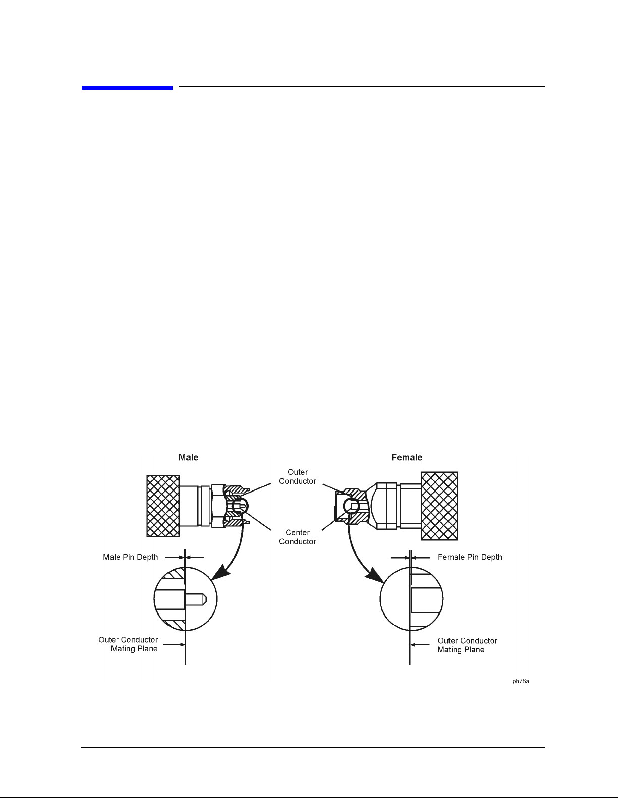
Pin depth is the distance the center conductor mating plane differs from being flush with
the outer conductor mating plane. See Figure 2-1. The pin depth of a connector can be in
one of two states: either protruding or rec essed.
Protrusion is the condition in which the center conductor extends beyond the outer
conductor mating plane. This condition will indicate a p ositive value on the connector gage.
Recession is the condition in which the center conductor is set back from the outer
conductor mating plane. T his condition will indicate a negative value on the connector
gage.
Figure 2-1 Connector Pin Depth
85056A 2-3

Specifications
Mechanical Characteristics
The pin depth value of each calibration device in the kit is not specified, but is an
important mechanical parameter. The electrical performance of the device depends, to
some extent, on its pin depth. The electrical specifications for each device in the kit take
into account the effect of pin depth on the device’s performance. Table 2-2 lists the typical
pin depths and measurement uncerta inties, and pr ovid es observed pin depth limits for the
devices in the kit. If the pin depth of a device does not measure within the observed pin
depth limits, it may be an indication that the device fails to meet electrical specifi cations.
Refer to Figure 2-1 on pag e 2-3 for a visual representation of proper pin depth (slightly
recessed).
Table 2-2 Pin Depth Limits
Device
Opens 0 to −0.0127 mm
Shorts 0 to −0.0127 mm
Fixe d loads −0.0025 to −0.0203 mm
Sliding loads 0 to −0.0127 mm
Adapters 0 to −0.0381 mm
a. Approximately +2 sigma to −2 sigma of gage uncertainty based on stud ies done at the
factory according to recom m ended procedures.
b. Observed pin depth limits are the range of observation limit s seen on the gage reading due
to measurement uncert ainty. The depth could still be within specif ications.
Typical Pin Dept h
0 to −0.00050 in
0 to −0.00050 in
−0.00010 to −0.00080 in
0 to −0.00050 in
0 to −0.00150 in
Measu rem e n t U n certa in ty
+0.0030 to −0.0030 mm
+0.00012 to −0. 00012 in
+0.0015 to −0.0015 mm
+0.00006 to −0. 00006 in
+0.0030 to −0.0030 mm
+0.00012 to −0. 00012 in
+0.0015 to −0.0015 mm
+0.00006 to −0. 00006 in
+0.0030 to −0.0030 mm
+0.00012 to −0. 00012 in
a
Observed Pin Depth Limits
+0.0030 to −0.0157 mm
+0.00012 to −0.000 62 in
+0.0015 to −0.0142 mm
+0.00006 to −0.000 56 in
+0.0005 to −0.0234 mm
+0.00002 to −0.000 92 in
+0.0015 to −0.0142 mm
+0.00006 to −0.000 56 in
+0.0030 to −0.0411 mm
+0.00012 to −0.001 62 in
b
2-4 85056A

Specifications
Electrical Specifications
Electrical Specifications
The electrical specif ications in Table 2-3 apply to the devices in your calibration kit when
connected with an Agilent precision interface.
Table 2-3 Electrical Specifications for 85056 A 2.4 mm Devices
Device Specifi cation Frequency (GHz)
Broadband loads Return loss ≥ 42 dΒ (ρ ≤ 0.00794) dc to ≤ 4
(male and female) Return loss ≥ 34 dΒ (ρ ≤ 0.01995) > 4 to ≤ 20
Return loss ≥ 30 dB (ρ ≤ 0.0316 2) > 20 to ≤ 26.5
Return loss ≥ 26 dB (ρ ≤ 0.0501 9) > 26.5 to ≤ 50
a
Sliding loads
(male and female) Return loss ≥ 40 dΒ (ρ ≤ 0.01000) > 20 to ≤ 36
Adapters Return loss ≥ 32 dΒ (ρ ≤ 0.02512) dc to ≤ 4
Offset opens
(male and female) ± 1.25 ° devia tion from nominal > 2 to ≤ 20
Offset shorts
(male and female) ± 1.25 ° devia tion from nominal > 2 to ≤ 20
b
b
Return loss ≥ 42 dΒ (ρ ≤ 0.00794) 4 to ≤ 20
Return loss ≥ 38 dB (ρ ≤ 0.0125 9) > 36 to ≤ 40
Return loss ≥ 36 dB (ρ ≤ 0.0158 5) > 40 to ≤ 50
Return loss ≥ 30dΒ (ρ ≤ 0.03162) > 4 to ≤ 26.5
Return loss ≥ 25dB (ρ ≤ 0.05623) > 26.5 to ≤ 40
Return loss ≥ 20 dB (ρ ≤ 0.1000 0) > 40 to ≤ 50
± 0.5 ° deviation from nominal
± 1.75 ° devia tion from nominal > 20 to ≤ 40
± 2.25 ° devia tion from nominal > 40 to ≤ 50
± 0.50 ° devia tion from nominal
± 1.5 ° deviat ion from nominal > 20 to ≤ 40
dc to ≤ 2
dc to ≤ 2
± 2.0 ° deviat ion from nominal > 40 to ≤ 50
a. The specifications for t he sliding load termination incl ude the quality of the airline
portions within t he sliding load combined with the effective stability of the sliding
element.
b. The specifications for the opens and shorts are given as allowed deviation from the
nominal model as defined in the standard definitions (see “Nominal Standard
Definitions” on pageA-8).
85056A 2-5

Specifications
Electrical Specifications
Certification
Agilent Technologies certifies that this product met its p ub li shed s peci fic ations a t the time
of shipment from the factory. Agilent further certifies that its calibration measurements
are traceable to the United States National Institute of Standards and Technology (NIST)
to the extent allowed by the institute’s calibration facility, and to the calibration facilities
of other International Standards Organization m embers. See “How Agilent Verifies the
Devices in Your Kit” on page 4-2 for m o re information.
2-6 85056A

3 Use, Maintenance, and Care of the
Devices
3-1

Use, Maintenance, and Care of the Devices
Electrostatic Discharge
Electrostatic Discharge
Protection against electrostatic discharge (ESD) is essential while connecting, inspecting,
or cleaning connectors attached to a static-sensitive ci rcuit (such as those found in test
sets).
Static electricity can build up on y our body and can easily damage sensitive internal
circuit elements when discharged. Static discharges too small to be felt can cause
permanent damage. Devices such as calibration c omponents and devices under test (DUT),
can also carry an electrostatic charge. To prevent damage to the test set, components, and
devices:
• Always wear a grounded wrist stra p h avi ng a 1 MΩ resistor in series with it when
handling components and devices or when making connections to the test set.
• Always use a grounded antistatic mat in front of your test equipment.
• Always wear a heel strap when working in an area with a conductive floor. If you are
uncertain about the conductivity of your floor, wear a heel strap.
Figure 3-1 shows a typical ESD protection setup using a grounded mat and wrist strap.
Refer to Chapter 6, “Rep laceable Parts,” for information on ordering supplies for ESD
protection.
Figure 3-1 ESD Protection Setup
3-2 85056A

Use, Maintenance, and Care of the Devices
Visual Inspection
Visual Inspection
Visual inspection and, if necessary, cleaning should be done every time a connection is
made. Metal particles from the connector threads may fall into the connector when it is
disconnected. One connection made with a dirty or damaged connector can damage both
connectors beyond repair.
In some cases, m a gnification is necessary to see damage to a connector; a magnifying
device with a magnificati on of ≥ 10× is recommended. However, not all defects that are
visible only under magnification wi ll affect the elec trical per formance of the connector. Use
the following guidelines when evaluating the i ntegrity of a connector.
Look for Obvious Defects and Damage First
Examine the connectors first for obvious defects and damage: badly worn plating on the
connector interface, deformed threads, or bent, broken, or misaligned center conductors.
Connector nuts should move smoothly and be free of burrs, loose metal particles, and
rough spots.
What Causes Connector Wear?
Connector wear is caused by connecting and disconnecting the devices. The more use a
connector gets, the faster it wears and degrades. The wear is greatly accelerated when
connectors are not kept clean, or are not connected properly.
Connector wear eventually d egra des performance of the dev ice. Calibration devices should
have a long life if their use is on the order of a few times per week. Replace d evices with
worn connectors.
The test port connectors on the network analyzer test s et may have many connections each
day, and are therefore more subject to wear. It is recommended that an adapter be used as
a test port saver to m inimize the wear on the test set’s test port connectors.
Inspect the Mating Plane Surfaces
Flat contact between the connectors at a ll point s on their mating plane sur faces is required
for a good connection. See Figure 2-1 on pag e 2-3. Look especially for deep scratches or
dents, and for dirt and metal particles on the connector mating plane surfaces. Also look
for signs of damage due to excessive or uneven wear or misalignment.
Light burnishing of the mating plane surfaces is normal, and is evident as light scratches
or shallow circular marks distributed more or less uniformly over the mating plane
surface. Other small defects and cosmetic imperfections are also normal. None of these
affect electrical or mechanical performance.
If a connector shows deep scratches or dents, particles clinging to the mating plane
surfaces, or uneven wear, clean and inspect it again. Devices with d amaged connectors
should be discarded. Determine the cause of damage before connecting a new, undamaged
connector in the same configuration.
85056A 3-3

Use, Maintenance, and Care of the Devices
Cleaning Connectors
Inspect Female Connectors
Inspect the contact fingers in the female center conductor carefully. These can be bent or
broken, and damage to them is not always easy to see. A connector with damaged contact
fingers will not make good electrical contact and must be repla ced.
NOTE This is particularly important when mating nonprecision to precision devices.
The female 2.4 mm connectors in this calibration kit are metrology-grade, precision
slotless connector s (PSC) . Prec isi on s lotl ess conne cto rs are used to improve accuracy. With
PSCs on test ports and standards, the accuracy achieved when measuring at 50 dB return
loss levels is comparable to using conventi onal slotted connectors measuring devices
having only 30 dB ret urn loss. This represents an accuracy improvement of a bout 10 times.
Conventional female center conductors are slotted and, when mated, are flared by the
male pin. Because physical dimensions determine connector impedance, this change in
physical dimension affects electrical performance, making it very difficult to perform
precision measurements with c onventional slotted female connectors.
The precision slotless connector was developed to eliminate this problem. The PSC has a
center conductor with a solid cylindrical shell, the outside diameter of which does not
change when mated. Instead, this center conductor has an internal contact that flexes to
accept the male pin.
Cleaning Connectors
Clean connectors are essential for ensuring the integrity of RF and microwave coaxial
connections.
1. Use Compressed Air or Nitrogen
WARNING Always use protective eyewear when using compressed air or
nitrogen.
Use compressed air (or nitrogen) to loosen particles on the connector mating plane
surfaces. Clean ai r cannot damage a connector or leave particles or residues behind.
You can use any source of clean, dry, low-pressure compressed air or nitrogen that has
an effective oil-vapor filter and liquid condensation trap placed just before the outlet
hose.
Ground the hose nozzle to prevent electrostatic discharge, and set the air pressure to
less than 414 kP a (60 ps i) to con trol the vel ocity of th e air stream. High- velocity s treams
of compressed air can cause electrostatic effects when directed into a connector. These
electrostatic effects can damage the device. Refer to “Electrostatic Disch arge” on
page 3-2 earlier in this chapter for additional information.
3-4 85056A
 Loading...