

Page 1
INSTRUCTION MANUAL
KEPCO
An ISO 9001 Company.
KIT
BIT 4886
FIRMWARE UPGRADE
1. DESCRIPTION
The Kepco KIT Model 219-0452 contains the firmware upgrade PROM to be installed in BIT 4886 Interface
Cards that have been previously installed in Kepco’s BOP 100-2DM-4886-25968 power supply. The Firmware update provides for Output shutdown, automatically setting the output to off if any of the following error
conditions is detected:
• Output voltage exceeds +- 60 millivolts of the programmed output setting.
• Output current exceeds the programmed current protect level.
• Output current exceeds the fixed current limit of 1.1 amperes.
The shutting down of the output shall set the appropriate status bits in the Status questionable register, the
Event Status Register and add the appropriate error messages to the error queue.
219-0452
This instruction sheet provides procedures for installing the new PROM, initializing the BIT 4886 card, and
updating the BIT 4886 manual with a new procedure for calibrating the BOP power supply and modification
and additions to the SCPI commands and queries used to communicate with the power supply.
2. INSTALLATION OF UPGRADE PROM
A. MATERIAL REQUIRED (SEE TABLE 1.)
TABLE 1. MATERIAL REQUIRED
MATERIAL LOCATION
PROM Provided in this Kit
Extractor Provided in this Kit
ESD (Electrostatic Discharge) wrist strap. Not Supplied
Phillips Screw Driver Not Supplied
Sense Resistor Not Supplied (see Table 3-4 on page 8)
Heat Sink (cable of dissipating 10 times the power rating of the sense resistor) Not Supplied
Sealant, Kepco P/N 201-0002
(Glyptol P/N 7526P, 7625R or 7625G or equivalent)
Microsoft Windows-based computer with National Instruments VISA software installed Not Supplied
Digital Voltmeter (capable of measuring 100.0005V
(Keithly 2010 multimeter or equivalent
Not Supplied
Not Supplied
B. UPGRADE PROCEDURE
QUANTITY
4
1
N/A
N/A
1
N/A
N/A
N/A
N/A
1. Remove a-c power to BOP by disconnecting line cord.
CAUTION: Take care not to damage ground strap connected to cover when removing cover. Ground
strap may be removed for convenience by removing attaching nut.
2. Remove BOP cover by removing 11 screws: (five from each side and one from the top (see Figure 1, Detail A).
KEPCO, INC. " 131-38 SANFORD AVENUE " FLUSHING, NY. 11352 U.S.A. " TEL (718) 461-7000 " FAX (718) 767-1102
http://www.kepcopower.com "
©2004, KEPCO, INC
Data subject to change without notice 228-1481 REV 3
email: hq@kepcopower.com
1
Page 2
3. Remove the BIT 4886 Interface card from the BOP as follows (See Figure 1):
NOTE:Numbers in circles of Figure 1 refer to numbered steps below:
Step 1. Unplug 3 pin Connector from Transformer at BIT 4886 Card, Location #3.
Step 2. Unplug Cable #2 (5-position connectors) from the BIT 4886 Interface Card.
Step 3. Unplug Cable #1 (18-position connectors) from the BIT 4886 Interface Card.
Step 4. Remove the knurled nuts and lockwashers securing the BIT 4886 Card to hex spacers and
remove BIT 4886 Card by sliding to front of BOP, then rotating away from A1.
FIGURE 1. BIT CARD REMOVAL
4. A brown IC socket located towards the rear of the unit contains the PROM. Locate the small depression
or notch in the PROM as shown in Figure 2. This is pin 1 of the PROM.
CAUTION: FAILURE TO USE AN ESD WRIST STRAP MAY DAMAGE THE PROM!
5. Connect the wrist strap to the chassis of the BOP. Place the strap on your wrist as indicated by the
instructions for the wrist strap.
6. Touch the IC tube to the chassis of the BOP. Open one end.
7. Use the extractor and insert the hook, first into one slot and then the other, and gently pry out the PROM.
Place the PROM in the tube and close the tube.
KEPCO, INC. " 131-38 SANFORD AVENUE " FLUSHING, NY. 11352 U.S.A. " TEL (718) 461-7000 "
2
http://www.kepcopower.com " email: hq@kepcopower.com
228-1481 REV 3 021704
FAX (718) 767-1102
Page 3
FIGURE 2. PROM LOCATION
8. Open the other end of the IC tube and remove the replacement PROM from the tube.
9. Insert the PROM into the socket, insuring pin one is as shown in Figure 2.
10. Reclose the IC tube. Remove wrist strap and disconnect it from the BOP.
11. Reinstall the BIT 4886 Card in the BOP by reversing removal (Section. 2.B.3, steps 4 through 1). If removed
earlier, secure ground strap using nut, then Install cover using 11 screws (five at each side, one at top).
12. On the label at the rear of the BOP, after the revision number (XX-Y) mark “A” (XX-YA).
13. Reconnect power cord and turn on the BOP. Verify the unit beeps and initializes normally.
14. Initialize the BIT 4886 card per Section 3.
15. Calibrate the BOP power supply using the revised procedure found in Section 4.
3. INITIALIZATION OF THE BIT 4886 CARD
The initialization procedure uses the “soft” front panel which is part of the CVI driver for the BIT 4886 which can be
downloaded from the Kepco website at: www.kepcopower.com/all_bop.zip.
1. Unzip the files and doubleclick on setup.exe to install the driver. The bit_mdac folder will be added to the Start
- Programs folder. Doubleclick bit_mdac.exe to run the program, and refer to the visamdac.pdf in the bit_mdac
folder for details about using the soft front panel.
2. Connect GPIB cable from the rear of the BOP to a Microsoft Windows-based computer with National Instruments VISA software installed to BIT 4886 card and verify that BOP has standard PC-12 connector installed
(Figure 1).
3. Install the VISA driver per the text file included with the driver. At the Start-up screen (Figure 3) set the correct
GPIB Address and click CONNECT. Upon successful initialization the initialization window closes and the
Power Supply Type field of the Start-up window (Figure 3) shows BIT 4886. Click Continue.
4. Refer to Figure 4 and enter the following information:
• Select Model: BOP 100-2.
• Serial Number: Enter serial number found on the rear nameplate of BOP power supply.
• Option Number: Enter 25968
KEPCO, INC. " 131-38 SANFORD AVENUE " FLUSHING, NY. 11352 U.S.A. " TEL (718) 461-7000 "
http://www.kepcopower.com " email: hq@kepcopower.com
021704 228-1481 REV 3
FAX (718) 767-1102
3
Page 4
• Press the Initialize Card button
NOTE: If initialization fails and an error message is displayed, repeat step 3, making sure that the
proper information is entered, and the new PROM was installed
FIGURE 3. VISA DRIVER START-UP. FIGURE 4. BIT 4886 CARD INITIALIZATION
USING VISA DRIVER
5. After initialization, proceed to revised PAR. 3.3 to calibrate the upgraded unit.
4. BIT 4886 INSTRUCTION MANUAL CHANGES
A. REPLACE PAR. 3.3 CALIBRATION (INCLUDING TABLES 3-1 THROUGH 3-3 AND FIGURES 3-3
AND 3-4) WITH THE FOLLOWING (FIGURE 3-2 UNCHANGED, INCLUDED FOR CLARITY):
NOTE: ALL SENSE RESISTORS MUST BE MOUNTED
ON A HEATSINK WITH A MINIMUM SURFACE
AREA OF 36 SQUARE INCHES TO MAINTAIN
THERMAL STABILITY DURING CALIBRATION.
FIGURE 3-2. CURRENT SHUNT CONNECTIONS
KEPCO, INC. " 131-38 SANFORD AVENUE " FLUSHING, NY. 11352 U.S.A. " TEL (718) 461-7000 "
4
http://www.kepcopower.com " email: hq@kepcopower.com
228-1481 REV 3 021704
FAX (718) 767-1102
Page 5
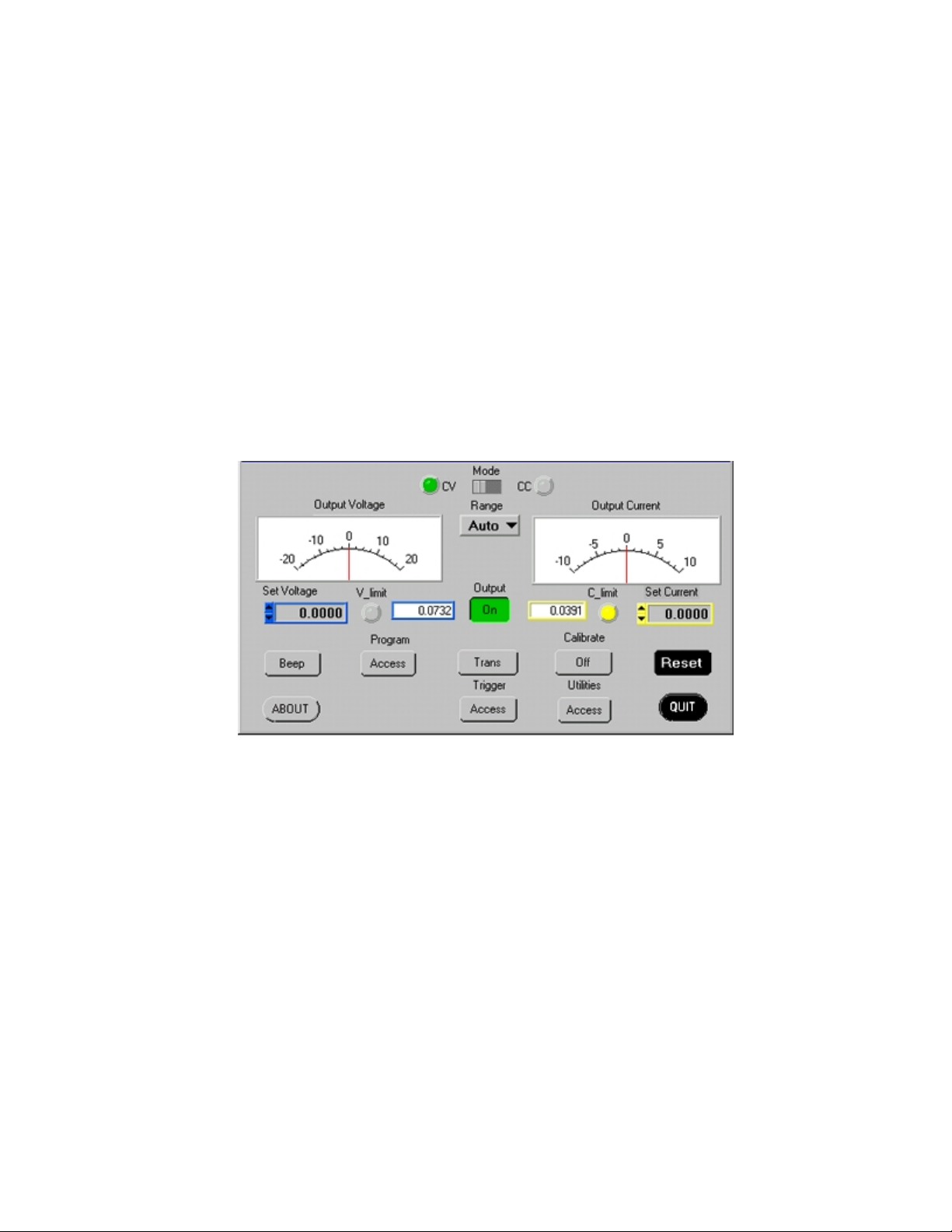
3.3 CALIBRATION OF BIT 4886 INTERFACE CARD USING THE VISA DRIVER SOFT PANEL
Calibration of the BIT 4886 card installed in the BOP 100-2DM-4886-25698 is performed using SCPI commands implemented through the Instrument driver. The driver provides a graphical interface with informational displays and prompts which lead you through the calibration of the BIT 4886 card. This VISA
compliant driver works with many GPIB cards from suppliers like National Instruments and Hewlett-Packard.
NOTE: PC-12 connector (See Figure 1) must be installed for BOP to function.
3.3.1 CALIBRATION USING THE VISA DRIVER SOFT PANEL
The following calibration procedure uses the “soft” front panel which is part of the CVI driver for the BIT
4886, Model 25968 which can be downloaded from the Kepco website at:
www.kepcopower.com/all_bop.zip:
Unzip the files and doubleclick on setup.exe to install the driver. The bit_mdac folder will be added to the
Start - Programs folder. Doubleclick bit_mdac.exe to run the program, and refer to the visamdac.pdf in the
bit_mdac folder for details about using the soft front panel.
FIGURE 3-3. MAIN PANEL
3.3.1.1 CALIBRATION BASICS
CAUTION: Before performing calibration, set BOP OUTPUT to OFF and connect short across BOP out-
put, then set OUTPUT to ON and Voltage to 10V. It is necessary to wait 10 minutes before
calibrating the unit to allow for thermal stabilization. After 10 minutes, set OUTPUT to
OFF and remove short from BOP output, then proceed with calibration.
All adjustments are done using the six arrow buttons of the Calibration Panel (see Figure 3-4 and Table 3-
1). The double arrow buttons
time; the ! and " buttons either increase (") or decrease (!) the output one step at a time. The triple
arrow buttons <<<— and —>>> either increase (—>>>) or decrease (<<<—) the output 80 steps at a time
!, "
The
For MAX and MIN Calibrations fine adjustment is done using the
can not be set within the specified tolerance using the fine adjustment, use the coarse adjustment to
increase (—>>>) or decrease (<<<—) the output. as needed, then use the fine adjust buttons to set the
value within tolerance.Where large adjustment is necessary, <<<— and —>>> can be used first to bring the
output close before using the
KEPCO, INC. " 131-38 SANFORD AVENUE " FLUSHING, NY. 11352 U.S.A. " TEL (718) 461-7000 "
021704 228-1481 REV 3
, !, and " buttons only work within the 80-step window established by <<<— and —>>>.
http://www.kepcopower.com " email: hq@kepcopower.com
!
and " either increase (") or decrease (!) the output five steps at a
!, "
, !, and " buttons.
!, "
, !, and " buttons. If the value
FAX (718) 767-1102
5
Page 6
FIGURE 3-4. CALIBRATION PANEL
TABLE 3-1. CALIBRATION PANEL FUNCTIONS
BUTTON OR WINDOW Function
START button Initiates calibration
Text box (Adjacent to START button) Used to enter unit password
VOLT button Initiates Voltage calibration
CURR button Initiates Current calibration
Message box (below VOLT buttons) Provides instructions about the calibration process.
White text window (above OK button) Displays the parameter currently being calibrated.
Á button Fine Adjustment - Decreases the output value by one LSB.
Ë button Fine Adjustment - Increases the output value by one LSB.
button Adjustment - Decreases the output value by five LSBs.
!
button Adjustment - Decreases the output value by five LSBs.
8
<<<— button Coarse Adjustment - Decreases the output value by 80 LSBs.
—>>> button Coarse Adjustment - Increases the output value by 80 LSBs.
OK button Enters the value displayed in the white text window
3.3.1.2 CALIBRATION PROCEDURE
1. Click on the Calibration Off button on the main panel (see Figure 3-3).This will open a calibration panel
(see Figure 3-4 and Table 3-1) that allows calibration in either voltage or current mode.
2. The password (DEFAULT) has been set at the factory. If it has not been changed, it will be displayed in
the box adjacent to the Start button on the right side of the panel. If the password has been changed
from DEFAULT, substitute the proper password in the box adjacent to the Start button and click the
Start button. If the password has been forgotten, consult factory. If the password is correct, the Volt and
Curr buttons will become active. Otherwise the message ERROR! - Wrong Password is displayed
and you must enter the correct password and click Start again.
3. For Voltage Calibration, click Volt button. The text window reads Volt ZERO and the message Adjust
for ZERO R81 (Eo Zero) on BOP A1 card. is displayed.
KEPCO, INC. " 131-38 SANFORD AVENUE " FLUSHING, NY. 11352 U.S.A. " TEL (718) 461-7000 "
http://www.kepcopower.com " email: hq@kepcopower.com
6
FAX (718) 767-1102
228-1481 REV 3 021704
Page 7

4. Connect a DVM to the output of the unit and adjust the R81 Potentiometer on A1 board of BOP until the
DVM reads the voltage specified in Table 3-2 for Low Range Zero, then click OK button.
NOTE: Use external DVM for all measurements.
TABLE 3-2. CALIBRATION MEASUREMENTS AND TOLERANCES - VOLTAGE
MODEL
BOP 100-2M
LOW
RANGE
ZERO
PAR. 3.3.1
STEP 4
0V
±0.0001V
VOLT
ZERO
PAR. 3.3.1
STEP 5
0V
±0.001V
HIGH
RANGE
ACCURACY
PAR. 3.3.1
STEP 6 and 7
100V (MAX)
-100V (MIN)
±0.0075
LOW
RANGE
ACCURACY
PAR. 3.3.1
STEPS 8, 9
25V (MAX)
-25V (MIN)
±0.002
5. The text window reads Volt ZERO and the message Measure and Adjust. is displayed. Using the !
and " and
!
and " buttons (see PAR. 3.3.1.1), adjust the output until the DVM reads the voltage
specified in Table 3-2 for VOLT ZERO, then click OK button.
6. The text window reads Volt MAX and the message Measure and Adjust. is displayed. Using the !
and " and
!
and " buttons (see PAR. 3.3.1.1), adjust until DVM reading is as specified in Table 3-2
for High Range Accuracy. Click OK when done.
7. The text window reads Volt MIN and the message Measure and Adjust. is displayed. Using the !
and " and
!
and " buttons (see PAR. 3.3.1.1), adjust until DVM reading is as specified in Table 3-2
for High Range Accuracy, then click OK button. NOTE: If the <<<— or —>>> button is depressed, proceed to step 6 after clicking OK.
8. The text window reads LVolt MAX and the message Measure and Adjust. is displayed. Using the !
and " and
!
and " buttons (see PAR. 3.3.1.1), adjust output until DVM reads voltage specified in
Table 3-2 for Low Range Accuracy, then click OK button.
9. The text window reads LVolt MIN and the message Measure and Adjust. is displayed. Using the !
and " and
!
and " buttons (see PAR. 3.3.1.1), adjust until DVM reads voltage specified in Table 32 for Low Range Accuracy, then click OK button. NOTE: If the <<<— or —>>> button is depressed, proceed to step 8 after clicking OK.
10.Voltage calibration is complete. If desired, the voltage calibration can be repeated by clicking Volt at the
calibration panel (Figure 3-3). If current calibration is not necessary, proceed to step 19.
11.At the calibration panel (Figure 3-3) click CURR to begin current calibration of the unit. Connect CALI-
BRATION RESISTOR! window opens.
12.Connect load (see Table 3-4) across the output of the unit and connect DVM across the load as shown
in Figure 3-2. Voltage measurements must be converted to Amperes using Ohm’s law, E = IR. Click OK
button to close Connect CALIBRATION RESISTOR window.
13.The test window reads Curr ZERO and the message Adjust for ZERO R83 (Io Zero) on BOP A1 card.
will be displayed.
14.Adjust the R83 Potentiometer on A1 board of BOP, until the external DVM reads voltage specified in
Table 3-3, then click OK button.
15.The text window reads Curr MAX and the message Measure and Adjust. is displayed. Using the !
and " and
!
and " buttons (see PAR. 3.3.1.1), adjust output until DVM reads the voltage specified
in Table 3-3, then click OK button.
KEPCO, INC. " 131-38 SANFORD AVENUE " FLUSHING, NY. 11352 U.S.A. " TEL (718) 461-7000 "
http://www.kepcopower.com " email: hq@kepcopower.com
021704 228-1481 REV 3
FAX (718) 767-1102
7
Page 8

TABLE 3-3. CALIBRATION MEASUREMENTS AND TOLERANCES - CURRENT
SENSE
RESISTOR
MODEL
BOP 100-2M
REFER TO NOTES IF
EXACT SENSE RESISTOR
VALUE IS KNOWN.
USE SPACE PROVIDED
AT RIGHT FOR
CALCULATED VALUES.
NOTES: The following formulas are used to calculate proper calibration values if the
exact Sense Resistor value is known.
R
A. Adjust to 0V ±(
B. Adjust V to (
C. Adjust V to (
SENSE
=
the measured value of the sense resistor to 6 places (minimum).
(SEE NOTE
TABLE 3-4)
R
SENSE
R
SENSE
R
SENSE
VAL UE
AND
1 Ohm
R
SENSE
SEE
NOTES.
) (0.00005)
) (2) ± (
) (2) ± (
CURRENT
ZERO
PAR. 3.3.1
STEP 14
0V
±0.00005V
SEE
NOTE A.
R
SENSE
R
SENSE
) (0.00015)
) (0.0006)
HIGH
CURRENT
ACCURACY
PAR. 3.3.1
STEP 15, 16
2V (MAX)
-2V (MIN)
±0.00015V
SEE
NOTE B.
CURRENT
PROTECT
ACCURACY
PAR. 3.3.1
STEP 17
2V (MAX)
±0.0006V
SEE
NOTE C.
TABLE 3-4. SUGGESTED SENSE RESISTORS
VALUE KEPCO PART NO. MANUFACTURER MANUFACTURER PART NO.
1 OHM 115-2996 ISOTEK RUG-Z-1R00-0.1 TK10
NOTES:
1. For Sense resistor values not listed, calculate the nominal value and tolerance as follows:
Nominal Value (Volts) = Actual Sense resistor resistance (Ohms) (measured to 8 places) x rated current (Amps)
Tolerance (Volts) = Nominal value (Volts)/32000
2. Sense resistor must be used with heat sink capable of dissipating 10 times rated power with a minimum surface area of 36 square
inches to maintain thermal stability during calibration.
16.The text window reads Curr MIN and the message Measure and Adjust. is displayed. Using the !
and " and
!
and " buttons (see PAR. 3.3.1.1), adjust until DVM reading is as specified in Table 3-3.
NOTE: If the <<<— or —>>> button is depressed, proceed to step 15 after clicking OK.
17.The text window reads Curr PROTECT and the message Measure and Adjust. is displayed. Using the
! and " and
!
and " buttons (see PAR. 3.3.1.1), adjust until DVM reading is as specified in Table
3-3. Click OK when done.
18.Current calibration is complete. If desired, the current calibration can be repeated by clicking Curr at the
calibration panel (Figure 3-4).
19.To exit Calibration, click on the Calibration On button on the main panel (Figure 3-3). This will open a
panel that allows the calibration to be saved. Click SAVE to save the calibration constants (both voltage
and current), or CANCEL to return to the old calibration.
20.Upon completing calibration, seal adjustment potentiometers A1R81 and A1R83 on BOP using sealant
(see Table 1).
KEPCO, INC. " 131-38 SANFORD AVENUE " FLUSHING, NY. 11352 U.S.A. " TEL (718) 461-7000 "
8
http://www.kepcopower.com " email: hq@kepcopower.com
228-1481 REV 3 021704
FAX (718) 767-1102
Page 9

B. REPLACE PAR. 5.2, 5.2.1, AND 5.2.2 AS FOLLOWS:
5.2 ENHANCED OPERATION
The following paragraphs describe options that will permanently modify the behavior of the BIT 4886 and
associated BOP power supply. Although these options use SCPI commands, they are not intended to be
used during normal programming of the BOP output.
The commands described in the following paragraphs affect only RAM variables. The power up state of the
variables is retrieved from the FLASH EEPROM. The command MEMORY:UPDATE can be used to copy
this RAM information to the FLASH EEPROM. The WINDOW variable is stored using the command
MEM:UPDATE SHUTDOWN and the other variables, including the DIAG:SAV command, use the command
MEMORY:UPDATE INTERFACE
5.2.1 ERROR DETECTION
The BIT 4886 card has the ability to alter the way the unit responds to detection of load and settings errors.
The default behavior is for the BIT 4886 to measure the main channel and verify that it is within the specified channel tolerances of the BOP, setting the appropriate bits in the Status Questionable register. This
default behavior is established by the SYST:SEC:IMM command and the factory default window of 32
LSBs.
The default behavior can be modified using the DIAG:ERR, DIAG:ONL, DIAG:OFFL AND DIAG:WIN commands listed in Table 5-1 so that device errors are generated for conditions such as window exceeded, output current limit at setting and output current exceeding a hard limit. These errors can also be used to force
the unit to go to an output off state upon detecting the errors. The behavior is altered, the new setting is
stored in RAM and it remains in effect until a power off/power on cycle. The settings can be saved for power
up by sending the MEMORY:UPDATE SHUTDOWN command. Error responses are listed in Table 5-1.
5.2.2 LIMIT CHANNEL CONTROL
The unit supports three limit settings for the output off state. The standard configuration is for the limits to be
set to the minimum levels which causes the output not to vary beyond the BOX limits defined in the BOP
manual. The limits can also be set to maximum or 110% of rated voltage or current. This is useful for battery
operation. These limit settings are established by the DIAG:OUTPut command. With other types of devices,
it is possible to set the output off limit channels to be at any level by using the DIAG:OFFLimit commands to
establish the limit for the output off state. DIAG:OUTP n
when the output is set to OFF. n = 0 is the default. This sets both voltage and current limit channels to 0
when the output is off. n = 1 sets voltage limit to maximum when the output is off. n = 2 sets the current limit
to the maximum when the output is off. Bits 2 and 3 of the hex character allow the DIAG:OFFLimit commands to establish a specific voltage limit and current limit, respectively, when the output is off. Bits 0 and 2
or bits 1 and 3 should not be set at the same time since the maximum setting will override the value specified by DIAG:OFFLimit. The SYST:SEC:IMM command sets DIAG:OUTP n = 0. The variables are stored in
non-volatile EEPROM by the command MEMORY:UPDATE INTERFACE.
(see Table 5-1) controls the limit DAC values
H
KEPCO, INC. " 131-38 SANFORD AVENUE " FLUSHING, NY. 11352 U.S.A. " TEL (718) 461-7000 "
http://www.kepcopower.com " email: hq@kepcopower.com
021704 228-1481 REV 3
FAX (718) 767-1102
9
Page 10

C. REPLACE TABLE 5-1 TO UPDATE DIAG: COMMANDS AND QUERIES
TABLE 5-1. ENHANCED OPERATION - ERROR RESPONSE
COMMAND QUERY DESCRIPTION
DIAG:ERR:CURR xx
(xx =hex values from 00
to FF)
DIAG:ERR:VOLT xx
(xx =hex values from 00
to FF)
DIAG:OFFLimit:CURR xx
(xx = decimal value)
DIAG:ERR:CURR? Allows both current protect and current limit functionality.
Bit 7 - when set will establish a fixed Current Limit level when output is ON.
Bit 6 - when set enables the current protection error logic
Bit 5 - when set enables Current Protect error bit in ESR/ESE register
Bit 4 - when set causes the power up and reset state of the ESE register to
be as follows: ESE - 72 if bit 5 set, 8 if not set.
Bit 3 - when set allows a current protect error to create an error message of
“303 - Current above Protection limit.”
Bit 2 - when set causes a current protect error to set the output to off.
Bit 1 - when sets allows a current measurement in current mode to generate
a “Device Error” message.
Bit 0 - when set enables a current measurement error in current mode to
shut down unit.
The query provides one byte which indicates the current limit setting.
DIAG:ERR:VOLT? Allows voltage protect and voltage limit functionality.
Bit 7 - when set establishes a fixed Voltage Limit level when output is ON.
Bit 6 - when set enables the voltage protection error logic
Bit 3 - when set allows a voltage protect error to create an error message of
“304 - Voltage above Protection limit”
Bit 2 - when set causes a voltage protect error to set the output to off
Bit 1 - when set allows a voltage measurement error in voltage mode to
generate a “Device Error” message.
Bit 0 - when set allows voltage “device error” message (see bit 1) to set the
output to off.
The query provides one byte which indicates the voltage limit setting.
DIAG:OFFLimit:CURR? The decimal value allows the user to establish the actual current limit DAC (digital to ana-
log converter) setting when the output is off and the unit is in voltage mode. This variable is only used when bit 4 of the DIAG:OUTP register is set. The value is calculated
using the equation:
Current expected /(Current max * 1.1) * 256.
The DVS standard setting is 128 derived from (1.1 / 2.2 ) * 256.
The query provides one byte which indicates the actual DAC current limit setting.
DIAG:OFFLimit:VOLT xx
(xx = decimal value)
DIAG:ONLimit:CURR xx
(xx = decimal value)
DIAG:ONLimit:VOLT xx
(xx = decimal value)
KEPCO, INC. " 131-38 SANFORD AVENUE " FLUSHING, NY. 11352 U.S.A. " TEL (718) 461-7000 "
10
DIAG:OFFLimit:VOLT? The decimal value allows the user to establish the actual voltage limit DAC (digital to ana-
DIAG:ONLimit:CURR? The decimal value allows the user to establish the actual current limit DAC (digital to ana-
DIAG:ONLimit:VOLT? The decimal value allows the user to establish the actual voltage limit DAC (digital to ana-
http://www.kepcopower.com " email: hq@kepcopower.com
log converter) setting when the output is off and the unit is in current mode. This variable is only used when bit 3 of the DIAG:OUTP register is set. The value is calculated
using the equation:
Voltage expected / Voltage max * 1.1) * 256
The DVS standard setting is 0.
The query provides one byte which indicates the actual DAC current limit setting.
log converter) setting when the output is on and the unit is in voltage mode. This variable is only used when bit 7 of the DIAG:ERR:CURR register is set. The value is
calculated using the equation:
Current expected /(Current max * 1.1) * 256.
The DVS standard setting is 128 derived from (1.1 / 2.2 ) * 256.
The query provides one byte which indicates the actual DAC current limit setting.
log converter) setting when the output is on and the unit is in current mode. This variable is only used when bit 7 of the DIAG:ERR:VOLT register is set. The value is
calculated using the equation:
Voltage expected / Voltage max * 1.1) * 256
The DVS standard setting is 0.
The query provides one byte which indicates the actual DAC current limit setting.
FAX (718) 767-1102
228-1481 REV 3 021704
Page 11
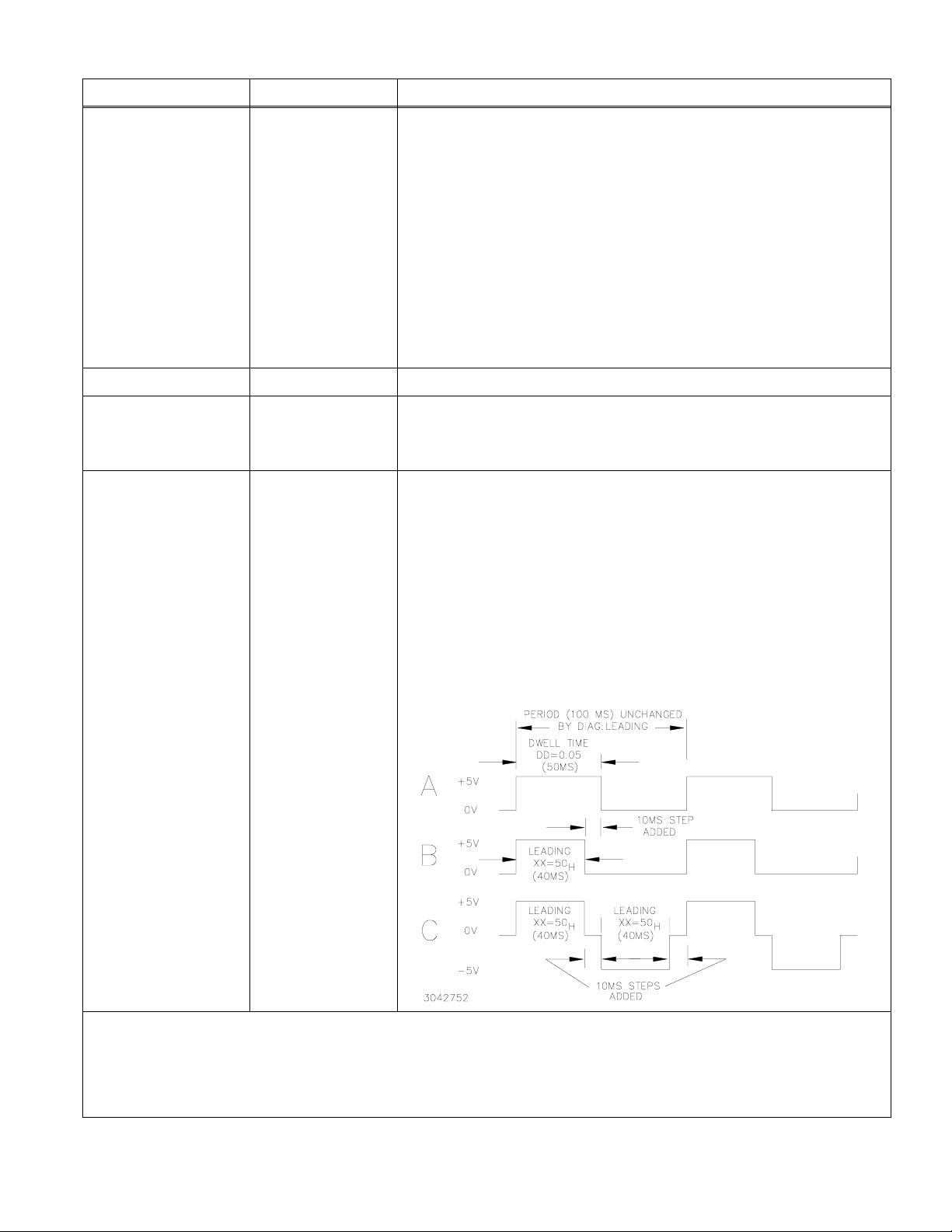
TABLE 5-1. ENHANCED OPERATION - ERROR RESPONSE (CONTINUED)
COMMAND QUERY DESCRIPTION
DIAG:OUTP n
(n = hex character)
DIAG:SAV n/a DIAG:SAV stores variables established by SYST:SET. (See PAR. 5.2.3 and B.82)
DIAG:WIN xx
(xx = hex value from 10
1
to 40)
DIAG:LEADING xx
(xx is the time in half milliseconds increments)
(hex)
DIAG:OUTP?
(Returns hex character)
DIAG:WIN?
(Returns window
value xx (hex)
DIAG:LEADING?
returns xx (hex), the
time in half milliseconds increments)
DIAG:OUTP n controls the limit DAC values when the output is set to OFF. The values
can either be set to maximum or to a user determined limit value (using the
DIAG:OFFLimit commands. The SYST:SEC:IMM command sets DIAG:OUTP n = 0.
DIAG:OUTP 0 = the default. This sets both voltage and current limit channels to 0 when
the output is off. The four bits of the hex character are defined as follows:
Bit 0 = 1 sets voltage limit to maximum when in Voltage mode and the output is off.
Bit 1 = 1 sets current limit to maximum when in Current mode and the output is off.
Bit 2 = 1 sets voltage limit to value determined by the DIAG:OFFLimit:VOLT command when the output is off.
Bit 3 = 1 sets current limit to value determined by the DIAG:OFFLimit:CURR command when the output is off.
For example, DIAG:OUTP 3 = sets both voltage and current limit to maximum. This
can be useful for battery applications where the limit channel can allow the battery to
discharge the battery voltage. Using both the maximum and DIAG:OFFLimit options
(e.g., bits 0 and 2) at the same time is not recommended - the maximum value overrides the DIAG:OFFLimit setting.
Allows user to specify value in LSB’s for error window used for detection of output voltage
or output current measurement errors (default = 32). Error window value can only be
set between 16 (10 Hex) and 64 (40 Hex) using one two-digit hex character (xx)
Query returns 2-digit hex character xx.
xx establishes max dwell time for a two-step list. If the dwell time DD for the two-step list
exceeds xx, a step is inserted with voltage = 0V for (DD - xx). MSTS default = 50.
Consider the following:
LIST:VOLT 0,5 Two step list, 0V then 5V.
LIST:DWEL .05 Dwell time of 50 ms
LIST:COUNT 0 Repeat continuously.
OUTP ON Output enabled.
VOLT:MODE LIST Run program
The above list would normally produce a continuous square wave, 50ms at 0V, 50ms
at 5V (Fig A). If DIAG:LEADING 50 (40 ms) is issued, the square wave changes to
60ms at 0V, 40ms at 5V as follows: the first 1/2 cycle = 50ms at 0V, the second 1/2
cycle = 40ms (the limit set by DIAG:LEADING) at 5V, then 10ms (50 - 40 = 10) at 0V
(Fig B). If LIST:VOLT 0,5 is changed to LIST:VOLT -5,5 both 1/2 cycles will show
10ms steps at 0V (Fig C).
1
.
1 The default window value of 32 indicates a 32 LSB margin for error during readback. The value for Readback is arrived at by taking 16 samples
of voltage or current and averaging them. A readback error is produced when the calculated readback value (with calibration constants applied)
exceeds the maximum readback (calculated readback + error window) or minimum readback (calculated readback – error window). Increasing
the error window can avoid undesired errors. For example, in cases where the LIST command is used to produce a square wave output, overshoot inherent in the characteristics of the power supply can sometimes cause the readback average to increase enough to cause a readback
error. Increasing the error window allows the square wave to be generated without producing an error.
KEPCO, INC. " 131-38 SANFORD AVENUE " FLUSHING, NY. 11352 U.S.A. " TEL (718) 461-7000 "
http://www.kepcopower.com " email: hq@kepcopower.com
021704 228-1481 REV 3
FAX (718) 767-1102
11
Page 12

D. MODIFY TABLE A-2 TO ADD BIT 6 = PROTECTION ERROR
TABLE A-2. STANDARD EVENT STATUS ENABLE REGISTER AND STANDARD
EVENT STATUS REGISTER BITS
NU (Not Used)
CONDITION NU PE CME EXE DDE QUE NU OPC
BIT 76543210
VALUE 128 64 32 16 8 4 2 1
PE Protection Error
CME Command Error
EXE Execution Error
DDE Device Dependent Error
QUE Query Error
OPC Operation Complete
E. ADD THE FOLLOWING TO APPENDIX B
B.4A CALibrate:CPRotect COMMAND
CAL:CPR
Syntax: Short Form: CAL:CPR {MIN | MAX}
Long Form: CALibrate:CPRotect {MIN | MAX}
Description: Selects Current Protection limit calibration, only effective with power supply in Calibrate status. CAL:CPR
MAX selects maximum positive current protection limit calibration. CAL:CPR MIN selects maximum negative current protection limit calibration. Related Commands: CAL:STAT, CAL:ZERO, CAL:DATA, CAL:SAVE.
F. MODIFY TABLE B-5 TO ADD BIT 14 = PROTECTION ERROR
TABLE B-5. QUESTIONABLE EVENT REGISTER, QUESTIONABLE CONDITION REGISTER
AND QUESTIONABLE CONDITION ENABLE REGISTER BITS
CONDITION NU PE CE VE NU CM VM
BIT 15 14131211 - 2 10
VALUE 32,768 16,359 8192 4096 2048 - 4 2 1
PE PROTECTION ERROR
CE CURRENT ERROR
VE VOLTAGE ERROR
CM CURRENT MODE
VM VOLTAGE MODE
NU NOT USED
12
KEPCO, INC. " 131-38 SANFORD AVENUE " FLUSHING, NY. 11352 U.S.A. " TEL (718) 461-7000 "
http://www.kepcopower.com " email: hq@kepcopower.com
228-1481 REV 3 021704
FAX (718) 767-1102
 Loading...