

Page 1
INSTRUCTION MANUAL
An ISO 9001 Company.
ATE-DMG KEPCO
EXT. CONTROL
KIT
ATE-DMG
EXTERNAL CONTROL
FIELD UPGRADE KITS
219-0439, 219-0440, 219-0441, 219-0463
1. DESCRIPTION
Kepco Kits 219-0439 for ATE 36-30DMG, 219-0440 for ATE 100-10DMG, 219-0441 for ATE 25-40DMG and 219-0463 for ATE 7515DMG allows these models to be upgraded to accommodate external control of the output. Each kit contains a specially modified
PC-12 connector (adapter assembly A11) with associated interconnect cable and a PROM which upgrades the firmware.
2. INSTALLATION OF COMPONENTS
2.1 MATERIAL REQUIRED (SEE TABLE 1.)
TABLE 1. MATERIAL REQUIRED
MATERIAL PART NUMBER LOCATION QUANTITY
• PROM Replaces U16 in Board A7 Different with each kit Provided in this Kit 1
• Adapter assembly A11 with Interconnect cable. Different with each kit Provided in this Kit 1
• Instruction Manual KEPCO P/N 228-1469 Provided in this Kit 1
• ESD (Electrostatic Discharge) wrist strap (KEPCO P/N 114-0080) KEPCO P/N 114-0080 Provided in this Kit 1
• IC Extractor 114-0079 Provided in this Kit 1
• Phillips Screw Driver N/A Not Supplied N/A
2.2 DISASSEMBLY PROCEDURE
1. Turn power off, disconnect the unit from source power and remove line cord.
2. Remove the top cover of the unit by removing 20 screws as follows: two at top of the rear panel and nine on each side.
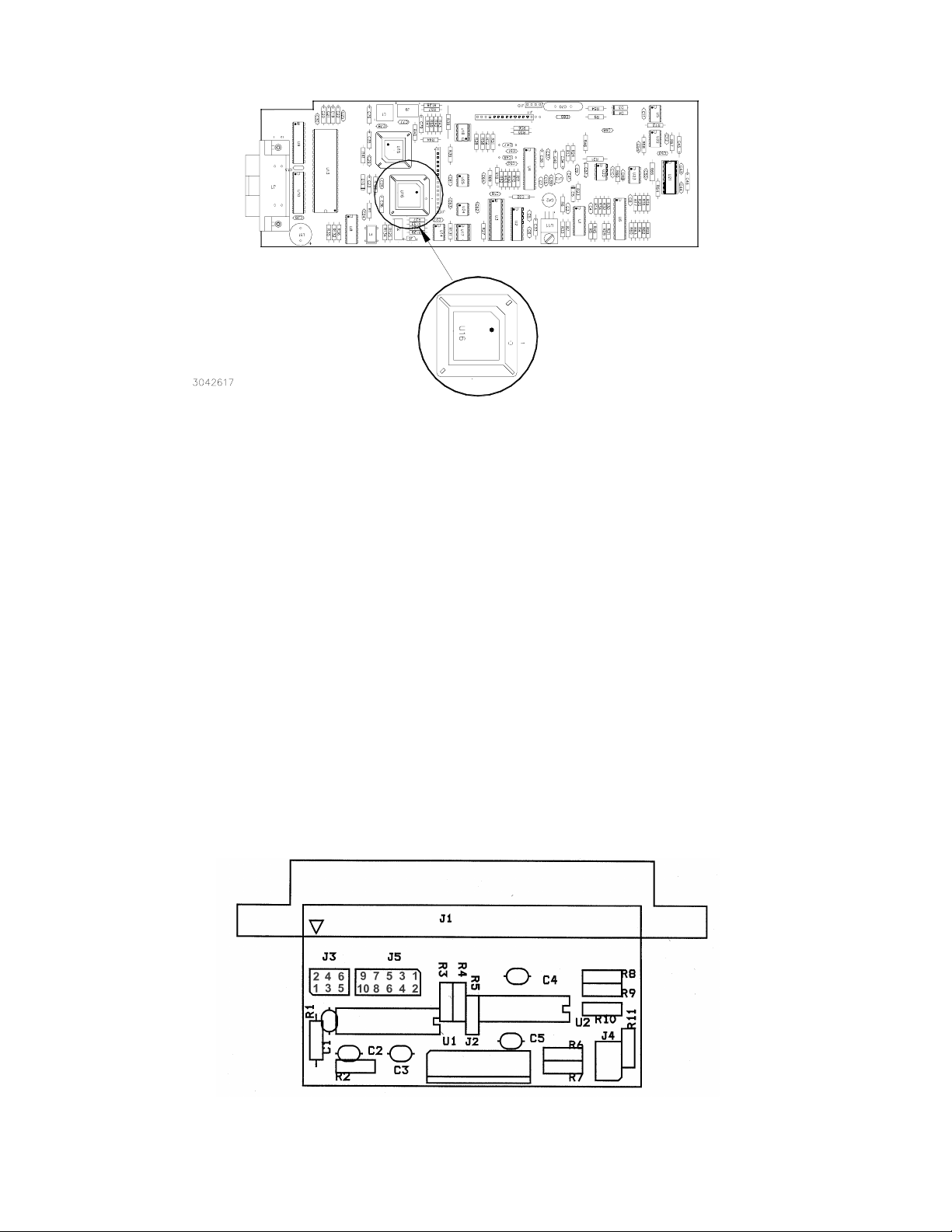
2.3 PROM REPLACEMENT PROCEDURE (SEE FIGURE 1)
NOTE: The PROM included in this Kit updates the firmware to Rev 6.3. If the firmware is already at Rev 6.3 or later, it is not
1. Locate PROM, U16 on Digital board A7 (see Figure 1).
2. Take the wrist strap from kit and use the peel and stick area to connect the wrist strap to the chassis of the ATE-DMG.
3. Touch the IC tube to the chassis of the ATE-DMG. Open one end.
4. Pry out the PROM using an IC extractor. Insert the hook, first into one slot and then the other, and gently pry out the PROM.
necessary to replace the PROM. Skip to PAR. 2.4 for Adapter Assembly replacement. Verify the PROM revision by
pressing the MENU Key on the ATE-DMG keypad until the display shows the operating configuration. (See PAR. 2.8 of
the ATE-DMG Technical Manual.)
Place the wrist strap on your arm as indicated by the instructions for the wrist strap.
Place the PROM in the tube and close the tube.
5. Open the other end of the IC tube and remove the replacement PROM from the tube.
6. Insert the PROM into the socket, ensuring the dot is oriented as shown in Figure 1.
KEPCO, INC. 131-38 SANFORD AVENUE FLUSHING, NY. 11352 U.S.A. TEL (718) 461-7000 FAX (718) 767-1102
http://www.kepcopower.com email: hq@kepcopower.com
©2005, KEPCO, INC 1
Data subject to change without notice 228-1469 REV 3
Page 2
7. Reclose the IC tube. Remove wrist strap and disconnect it from the ATE-DMG chassis.
8. Proceed to PAR. 2.4 to replace the Adapter Assembly
FIGURE 1. DIGITAL BOARD A7 PROM LOCATION
CAUTION:FAILURE TO USE THE ESD WRIST STRAP MAY DAMAGE THE PROM!
2.4 ADAPTER ASSEMBLY A11 REPLACEMENT PROCEDURE (SEE FIGURE 2)
NOTE: See PAR. 2.2 for disassembly.
1. Unplug interconnecting cable going to A7J1 from A11 Assembly.
2. Remove and discard A11 assembly and interconnecting cable assembly.
3. Install new A11 Assembly and connect new interconnecting cable from A11J2 to A7J1.
2.5 REASSEMBLY
1. Attach the cover to the chassis using 20 screws.
2. Install the power cord and connect the unit to source power, then proceed to PAR. 2.6 to initialize and calibrate the unit.
2.6 INITIALIZATION AND CALIBRATION
1. Turn on power supply. The unit will initialize with ENTER PS TYPE displayed on the LCD.
2. Use the keypad to enter the voltage followed by the current (e.g., for the ATE 25-40DMG, enter 2540), then press ENTER
(refer to Table 4-1 in ATE-DMG Service Manual).
3. The unit must then be calibrated by following the prompts displayed on the LCD (see Table 4-1 of ATE-DMG Service Manual).
FIGURE 2. ADAPTER ASSEMBLY A11, COMPONENT LOCATION
KEPCO, INC. 131-38 SANFORD AVENUE FLUSHING, NY. 11352 U.S.A. TEL (718) 461-7000 FAX (718) 767-1102
http://www.kepcopower.com email: hq@kepcopower.com
2 228-1469 REV 3 022305
Page 3

3. TECHNICAL MANUAL ADDITIONS
3.1 FAST/SLOW MODE
PAR. 2.7.4 steps 4 through 7 of the ATE-DMG Service Manual are replaced by the following: Remove jumper on adpater assembly
A11 between J3 pins 1 and 2; install jumpers between J3 pins 3 and 4 and between J3 pins 5 and 6. NOTE: Spare jumpers located
on J5.
3.2 USING THE EXTERNAL ANALOG REFERENCE
The following paragraphs describe the external control features available after the field upgrade kit has been installed.
The ATE-DMG now has the capability to control the output using a external d-c analog reference voltages. Analog references for
both voltage and current are required to produce an output. Two uncommited amplifiers (preamps”A” and “B”) included in the unit
can be used for signal conditioning. Each preamp has an inverting input (-), non-inverting input (+), and output, and a zero adjustment, and are accessable via A11J5 pins as shown in Figure 3. (For further details about Preamp “A” and “B” go to www.kepcopower.com/support and download the manual for ATE 1/4 Rack, 1/2 Rack 3/4 Rack or Full Rack, PAR’s 3-37 through 3-84.)
Connections to A11J5 can be made via discrete wires, a flat ribbon cable not exceeding 1 foot in length or by discrete wires terminated into crimp style pins inserted into a 5x2 housing (not supplied). The following parts are recommended, but not supplied: ribbon cable: AMP 746285-1 (Kepco P/N 142-0246); Housing for discrete wires: Molex 39-01-2100 (Kepco P/N 142-0434); Pins:
Molex 39-00-0039 (Kepco P/N 107-0290, 4 ea.).
NOTE: Connector A11J5 has two spare jumpers installed. When making connections to A11J5, move each spare jumper to a single pin of connector J3 (DO NOT SHORT J3 PINS).
1. Connect a 0 to 10V voltage reference to A11J5 pin 1 (pin 6 common); 0V programs the output voltage to zero, 10V programs output voltage to full scale.
2. Connect a 0 to 1V current reference to A11J5 pin 2 (pin 8 common), 0V programs the output current to zero, 1V programs
output current to full scale.
3. Turn on the external reference feature by sending the DIAG:EXT 01 command via the GPIB interface.
4. To access the external reference feature from the front panel, with the power supply in command entry status , press
MENU key 13 times until the top line of the display reads
line reads 0=Off, 1=On. Enter 1 to enable or 0 to disable and press ENTER to enable or disable the feature.
5. To access the feature from the GPIB the following commands are used.
To access external analog control from the GPIB, the following commands supplement those listed in Appendix B of the ATE-DMG
Technical Manual.
Extern. Ref On or Extern. Ref Off. and the bottom
B.91 [SOURce:]VOLTage:[:LEVel]MODE COMMAND VOLT:MODE
Syntax: Short Form: [SOUR:]VOLT[:LEV]:MODE {FIX | EXT}
Long Form: [SOURce:]VOLTage[:MODE {FIXed | EXTernal}
Description: Established whether control of the output voltage is via keypad or GPIB commands (FIXED) or via external
analog 0 to 10V reference (EXTERNAL). Setting is stored in NVRAM and retained upon subsequent power up.
B.92 [SOURce:]VOLTage:[:LEVel]MODE? QUERY VOLT:MODE?
Syntax: Short Form: [SOUR:]VOLT[:LEV]:MODE?
Long Form: [SOURce:]VOLTage[:LEVel]MODE]?
Return Value: FIXED or EXTERNAL
Description: Returns FIXED or EXTERNAL whether voltage control is from the keypad or GPIB interface (FIXED) or from
an external analog reference voltage (EXTERNAL).
B.93 [SOURce:]CURRent:[:LEVel]MODE COMMAND CURR:MODE
Syntax: Short Form: [SOUR:]CURR[:LEV]:MODE {FIX | EXT}
Long Form: [SOURce:]CURRent[:MODE {FIXed | EXTernal}
Description: Established whether control of the output current is via keypad or GPIB commands (FIXED) or via external
analog 0 to 1V reference (EXTERNAL). Setting is stored in NVRAM and retained upon subsequent power up.
KEPCO, INC. 131-38 SANFORD AVENUE FLUSHING, NY. 11352 U.S.A. TEL (718) 461-7000 FAX (718) 767-1102
022305 228-1469 REV 3 3
http://www.kepcopower.com email: hq@kepcopower.com
Page 4

B.94 [SOURce:]CURRent:[:LEVel]MODE? QUERY CURR:MODE?
n
Syntax: Short Form: [SOUR:]CURR[:LEV]:MODE?
Long Form: [SOURce:]CURRent[:LEVel]MODE]?
Return Value: FIXED or EXTERNAL
Description: Returns FIXED or EXTERNAL whether current control is from the keypad or GPIB interface (FIXED) or from
an external analog reference voltage (EXTERNAL).
B.95 DIAG:EXT COMMAND DIAG:EXT
Syntax: Short Form: DIAG:EXT <value>
Long Form: DIAG:EXT <value>
where <value> xx
HEX
Description: DIAG:EXT 01 initializes external analog control and 03 sets VOLT:MODE and CURR:MODE to EXTERNAL
DIAG:EXT 00 turns off the external analog control feature). Setting is stored in NVRAM and retained upon subsequent power up.
B.96 DIAG:EXT ? QUERY DIAG:EXT?
Syntax: Short Form: DIAG:EXT?
Long Form: DIAG:EXT]?
Return Value: 00
HEX
, 01
Description: Returns 00 when external analog control feature is disabled. Returns 01 when external analog control fea-
ture is enabled. Returns 03 when external analog control feature is enabled upon power up.
HEX
or 03
HEX
A11 J3
CONVERSION
12345
6
A11 J2
To A7
A11 J5
EXT_CMD
1
2
3
4
MODE
5
CMMD VOLTAGE 0 - 10V
6
CMMD CURRENT 0 - 10V
7
8
1
2
3
4
5
6
7
8
9
10
VOLTAGE 0 - 6V
INT/EXT
CURRENT 0 - 1V
GND
V_EXT
C_EXT
Aout
AA+
COMMON
B+
COMMON
BBout
GND
M15V
P15V
Bout
BAout
A-
A11 J1
1
2
1. Values for R1 and R2 are model specific
3
4
5
6
7
8
9
10
11
12
13
14
15
16
17
18
19
20
2. All Resistance in ohms.
21
22
3. Jumper Installed DMG option.
23
4. Jumper Installed for standard ATE or SN
24
25
option.
26
5. Jumper Installed for standard ATE.
27
28
6. Resistors R1,R2, R4, R6, R7, R8 installed
29
30
for DMG option.
31
32
33
7. For Standard ATE and SN option, external jumpers
34
35
should be installed between:
36
J5 P3-P4
37
38
J5 P9-P10
39
40
J4 P5-P6
41
8. For SLOW mode jumper should be installed between
42
43
J3 P1-P2
44
9. For FAST mode jumpers should be installed betwee
45
46
J3 P3-P4
47
48
J3 P5-P6
49
and jumper J3 P1-P2 should be removed.
50
10. For PAIRED units, remove jumper J4 P5-P6
A11 J4
GNDGND
1
2
3
4
5
6
NOTES
MODEL R2 R1
6-100 Not installed JUMPER
15-50 6980 11000
25-40 5620 18200
36-30 6980 35700
55-20 4220 35700
75-15 7870 90900
100-10 5760 90900
150-7 4220 100000
PAIRED ATE
M15V
R1
Note 1
P15V
R3
10K
R7
10K
Note 1
R10
10K
R2
GND
U1B
V_INT
V_EXT C_EXT
R9
10K
GND
5
6
R6
9
8
S1
D1
5
6
S2
D2
10
11
SEL
13
GNDV+V-
411
3
+
2
-
411
+
-
1K
P15V P15V
14
M15V
DG 390A
COMMON
P15V
U2A
V_INT
1
LM324
M15V
P15V
U2B
C_INT
7
LM324
M15V
C_INT
U1A
1
D1
3
D2
15
SEL
P15V
411
U2C
GND
10
+
9
-
LM324
M15V
P15V
411
U2D
GND
12
+
13
-
LM324
M15V
(Vl)
DG 390A
LAG NETWORK
16
S1
4
S2
12
8
MODE
14
R4
Note 4
P15V
R8
13K
C1.1C4
GND
.1
C3
C5
.1
.1
P15V
P15V
M15V
R5
Note 5
GND
A+
B+
GND
R11
Note 3
FIGURE 3. SCHEMATIC DIAGRAM
KEPCO, INC. 131-38 SANFORD AVENUE FLUSHING, NY. 11352 U.S.A. TEL (718) 461-7000 FAX (718) 767-1102
http://www.kepcopower.com email: hq@kepcopower.com
4 228-1469 REV 3 022305
 Loading...