

Page 1
OPERATOR’S MANUAL
BOP-GL 1KW
HIGH POWER BIPOLAR POWER SUPPLY
OPTIMIZED FOR INDUCTIVE LOADS
(LOW NOISE, RIPPLE, DRIFT AND TEMPERATURE COEFFICIENT)
KEPCO INC.
An ISO 9001 Company.
BOP-GL 1KW
POWER SUPPLY
ORDER NO.
IMPORTANT NOTES:
1) This manual is valid for the following Firmware Versions:
FIRMWARE VERSION NOTE.
3.05 and higher
2) A Change Page may be included at the end of the manual. All applicable changes and
revision number changes are documented with reference to the equipment serial numbers. Before using this Instruction Manual, check your equipment firmware version number to identify your model. If in doubt, contact your nearest Kepco Representative, or the
Kepco Documentation Office in New York, (718) 461-7000, requesting the correct revision
for your particular model and firmware version number.
3) The contents of this manual are protected by copyright. Reproduction of any part can be
made only with the specific written permission of Kepco, Inc.
Data subject to change without notice.
MODEL
©2014, KEPCO, INC
P/N 243-1293-s
KEPCO, INC. ! 131-38 SANFORD AVENUE ! FLUSHING, NY. 11355 U.S.A. ! TEL (718) 461-7000 ! FAX (718) 767-1102
email: hq@kepcopower.com ! World Wide Web: http://www.kepcopower.com
KEPCO®
THE POWER SUPPLIER™
Page 2

Page 3

Declaration of Conformity
Application of Council directives:
Standard to which Conformity is declared:
EN61010-1:1993 (Safety requirements for electrical equipment for measurement,
control and laboratory use)
Manufacturer's Name and Address:
Importer's Name and Address:
Type of Equipment:
Model No.:
73/23/EEC (LVD)
93/68/EEC (CE mark)
KEPCO INC.
131-38 SANFORD AVENUE
FLUSHING, N.Y. 11355 USA
P
O
C
E
V
I
T
A
T
N
E
S
E
R
P
E
R
Component Power Supply
[PRODUCT MODEL NUMBER]
Y
Year of Manufacture:
I, the undersigned, declare that the product specified above, when used in conjunction with the conditions of conformance set forth in the product instruction manual, complies with the requirements of the
Low Voltage Directive 73/23/EEC, which forms the basis for application of the CE Mark to this product.
Place: KEPCO Inc.
131-38 Sanford Ave.
Flushing, N.Y.11355 USA
Saul Kupferberg
(Full Name)
Date:
228-1348 DC-COMP/INST 022814 A
VP OF SALES
(position)
Page 4

Conditions of Conformance
When this product is used in applications governed by the requirements of the EEC, the following restrictions and conditions apply:
1. For European applications, requiring compliance to the Low Voltage Directive, 73/23/EEC, this power
supply is considered a component product, designed for “built in“ applications. Because it is incomplete in construction, the end product enclosure must provide for compliance to any remaining electrical safety requirements and act as a fire enclosure. (EN61010-1 Cl. 6, Cl. 7, Cl.8, Cl. 9 and EN610101 annex F)
2. This power supply is designed for stationary installation, with mains power applied via a detachable
power supply cord or via direct wiring to the source power terminal block.
3. This power supply is considered a Class 1 (earthed) product, and as such depends upon proper connection to protective earth for safety from electric shock. (EN61010-1 Cl. 6.5.4)
4. This power supply is intended for use as part of equipment meant for test, measurement and laboratory use, and is designed to operate from single phase, three wire power systems. This equipment
must be installed within a suitably wired equipment rack, utilizing a three wire (grounded) mains connection. See wiring section of this manual for complete electrical wiring instructions. (EN61010-1 Cl.
6.5.4 and Cl.6.10.1)
5. This power supply has secondary output circuits that are considered hazardous, and which exceed
100V d-c, able to deliver current greater than 10A d-c.
6. The output wiring terminals of this power supply have not been evaluated for field wiring and, therefore, must be properly configured by the end product manufacturer prior to use.
7. This power supply employs a supplementary circuit protector in the form of a circuit breaker mounted
on the front panel. This circuit breaker protects the power supply itself from damage in the event of a
fault condition. For complete circuit protection of the end product, as well as the building wiring, it is
required that a primary circuit protection device be fitted to the branch circuit wiring. (EN61010-1 Cl.
9.6.2)
8. Hazardous voltages are present within this power supply during normal operation. All operator adjustments to the product are made via externally accessible switches, controls and signal lines as specified within the product operating instructions. There are no user or operator serviceable parts within
the product enclosure. Refer all servicing to qualified and trained Kepco service technicians.
B 228-1529 COND/CONFORM 022814
Page 5
SAFETY INSTRUCTIONS
1. Installation, Operation and Service Precautions
This product is designed for use in accordance with EN 61010-1 and UL 3101 for Installation Category 2,
Pollution Degree 2. Hazardous voltages are present within this product during normal operation. The product should never be operated with the cover removed unless equivalent protection of the operator from
accidental contact with hazardous internal voltages is provided:
!
!
!
There are no operator serviceable parts or adjustments within the product enclosure.
Refer all servicing to trained service technician.
Source power must be removed from the product prior to performing any servicing.
This product is factory-wired for the nominal a-c mains voltage indicated on the rating nameplate located adjacent to the source power connection on the product's rear
panel. To reconfigure the product input for other nominal mains voltages as listed
herein, the product must be modified by a trained service technician.
2. Grounding
This product is a Class 1 device which utilizes protective earthing to ensure operator safety.
The PROTECTIVE EARTHING CONDUCTOR TERMINAL must be properly con-
!
nected prior to application of source power to the product (see instructions on installation herein) in order to ensure safety from electric shock.
PROTECTIVE EARTHING CONDUCTOR TERMINAL - This symbol indicates the
point on the product to which the protective earthing conductor must be attached.
EARTH (GROUND) TERMINAL - This symbol is used to indicate a point which is
connected to the PROTECTIVE EARTHING TERMINAL. The component installer/
assembler must ensure that this point is connected to the PROTECTIVE EARTHING TERMINAL.
CHASSIS TERMINAL -This symbol indicates frame (chassis) connection, which is
supplied as a point of convenience for performance purposes (see instructions on
grounding herein). This is not to be confused with the protective earthing point, and
may not be used in place of it.
3. Electric Shock Hazards
This product outputs hazardous voltage and energy levels as a function of normal operation. Operators
must be trained in its use and exercise caution as well as common sense during use to prevent accidental
shock.
This symbol appears adjacent to any external terminals at which hazardous voltage
!
228-1352 SAFETY - (COVER REMOVAL) 022814 C
levels as high as 500V d-c may exist in the course of normal or single fault conditions.
This symbol appears adjacent to any external terminals at which hazardous voltage
levels in excess of 500V d-c may exist in the course of normal or single fault conditions.
Page 6
OPERATOR
SAFETY INSTRUCTIONS
Read these safety instructions, as well as the applicable installation and operating instructions contained in
this manual before using the power supply.
WARNING
Do not touch the output terminals. The output is dangerous. Electric shock can cause injury or death.
Do not remove the cover or disassemble the unit. There are no operator serviceable components or
adjustments inside the unit. High voltage components inside the unit can cause serious injury even with
input power disconnected.
Service must be referred to authorized personnel. Using the power supply in a manner not specified by
Kepco. Inc. may impair the protection provided by the power supply. Observe all safety precautions noted
throughout this manual. The following table lists symbols used on the power supply or in this manual where
applicable.
The liquid in the LCD is hazardous: do not lick or swallow. Wash skin and clothes immediately and thoroughly upon exposure.
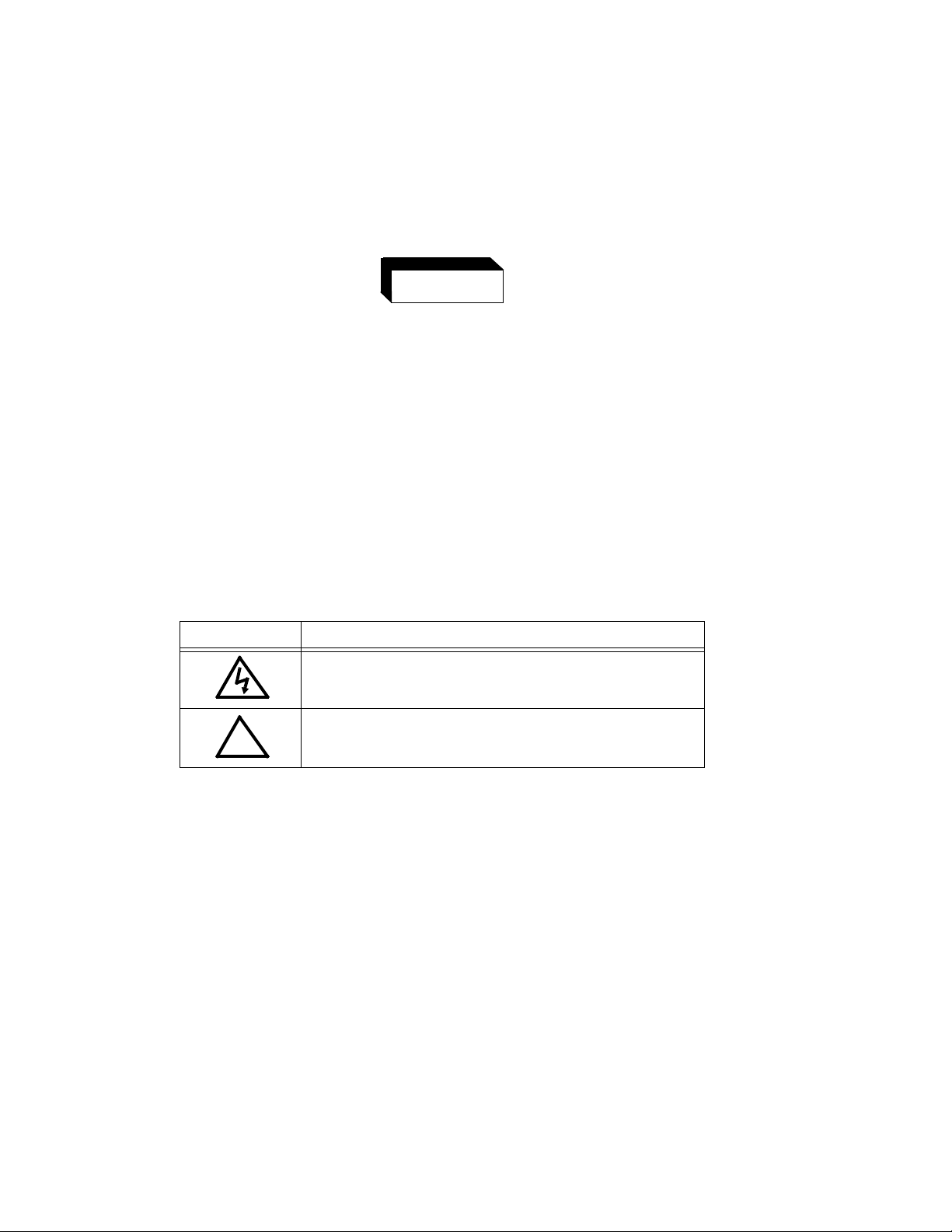
SAFETY SYMBOLS
SYMBOL Meaning
WARNING: RISK OF ELECTRIC SHOCK.
INDICATES THE POSSIBILITY OF BODILY INJURY OR DEATH.
CAUTION: REFER TO REFERENCED PROCEDURE.
!
INDICATES THE POSSIBILITY OF EQUIPMENT DAMAGE.
CAUTION
If this power supply is used in OEM equipment, the OEM equipment manufacturer is responsible for
attaching appropriate warning labels on the OEM equipment.
Operating the power supply outside the specified limits for input voltage, temperature, or other environmental conditions noted in this manual can damage the power supply and void the warranty.
DO NOT: wipe the front panel with hard materials, nor apply excessive force to the surface. DO NOT
expose to extended periods of bright sunshine or UV light.
Safety Messages
The BOP protection circuitry is designed to protect the load against unregulated high voltages and protect
the BOP from extensive damage in the event of a component failure. Refer to Table 1-2 for more information regarding the protection circuits.
D OP-SAFETY 022814
Page 7

LIST OF
WARNINGS AND CAUTIONS
PAGE WARNING/CAUTION
3-8 WARNING: For inductive loads, and especially superconducting magnet type loads,
the inherent offset of the BOP in the OFF state may generate significant
current in the circuit. A properly rated switch in parallel with a resistor
must be connected between the power supply and the load. The switch
must be open and voltage and current measurements at the output must
read 0V, 0A before removing or installing connections between BOP and
load.
3-9
3-9
4-8
2-8 CAUTION: it is recommended that source power of external equipment connected to
WARNING: For both inductive loads and constant-current-type active electronic
loads when the BOP output is set to OFF, a path is provided for absorbing
either the energy accumulated in the reactance of the load during the ON
state, or energy delivered by an electronic load. This prevents damage to
the load and power supply as well as providing safety for the user. However, In addition to the built-in safety features, constant-current-type active electronic loads must be adjusted to zero and voltage and current
measurements at the output must read 0V, minimum current, before handling the power supply-to-load connections.
WARNING: Accessing the BOP after the output is disabled in BATTERY mode is haz-
ardous because (1) high current arcing is possible and (2) either the external battery voltage, or the voltage (±Voltage Protection max) on the
BOP output terminals may be dangerous. Therefore, for battery and constant-voltage-type active electronic loads it is recommended that two
properly rated external switches be installed for safety: one in series with
the battery, and one across the BOP output. After the unit is set to OFF,
first open the switch in series with the battery, then close the switch
across the BOP output to ensure safety before handling BOP connections. When connecting the battery, the switch across the output should
be opened after the connections are complete and then the switch in series with the battery should be closed. If the constant-voltage-type active
electronic load is adjusted to zero before handling the power supply-toload connections, only the switch across the BOP output is required.
WARNING: The sense resistor will be dissipating full rated current of the BOP. If it is
hot to the touch, the sense resistor value, power rating and/or cooling are
incorrect; refer to PAR. 4.3 and Table 4-2.
the Analog Port be applied through an isolating transformer to avoid
ground loops or possible damage to the BOP due to incorrect equipment
a-c wiring (e.g., defeating of ground connection).
2-10 CAUTION: DO NOT repeatedly toggle the POWER circuit breaker/switch as this may
damage the unit.
2-11 CAUTION: DO NOT repeatedly toggle the POWER circuit breaker/switch as this may
damage the unit.
2-11 CAUTION: The rack must provide support at the rear (within 6 inches of the rear pan-
2-12 CAUTION: When working with active loads, the voltage or current of the active load
2-14 CAUTION: Never connect the load to the sense terminals. Monitoring instruments
2-14 CAUTION: Never connect the BOP OUTPUT terminal (or the load terminal tied to the
BOP 1KW OPR 2/28/14 E
el). Optional slides can also be used (see PAR. 2.4.2).
must not exceed the maximum voltage or current rating of the BOP. Otherwise the overvoltage or overcurrent protection will shut down the power supply.
(e.g., DVM, etc.) are the only external equipment that may be safely connected to the sense terminals.
OUTPUT terminal) to earth-ground. Otherwise, if the controlling device is
grounded, the BOP can be damaged by the protection limit output current
flowing inside the BOP along the programming signal return path.
Page 8

LIST OF
WARNINGS AND CAUTIONS
PAGE WARNING/CAUTION
2-14 CAUTION: Do not connect both the load and the programming device return (com-
mon) to earth-ground potential. Otherwise, If the COMMON power connection between the BOP and the load is lost, then the BOP can be
damaged by output current flowing inside the BOP along the programming signal return path.
2-14 CAUTION: The safety features incorporated into the BOP to handle energy from Ac-
tive loads are unable to protect the power supply or the load if input power to the BOP is lost or if the BOP Malfunctions. It is recommended that
the user monitor “Power OK” flag pins 3 and 4 of the external Protect Port
(see Table 2-5) and implement a fast-acting means of disconnecting capacitive loads or crowbarring inductive loads to prevent damage to both
the BOP and the load in the event of input power loss.
2-19 CAUTION: For both parallel and series configurations, remove links between (COM
S) and (COM OUT) terminals of all slaves to prevent damage to the unit
and maintain system accuracy. Make sure to accurately follow Figures 27 through 2-10 for proper connection of the units.
2-25 CAUTION: For both parallel and series configurations, remove links between (COM
S) and (COM OUT) terminals of all slaves to prevent damage to the unit
and maintain system accuracy. Make sure to accurately follow Figures 27 through 2-10 for proper connection of the units.
3-1 CAUTION: Before connecting a load, note that the unit is will power-up with the con-
figuration set by the power-up switches accessible through the top cover
(see Table 2-2 for switch settings). Verify that these power-up settings are
compatible with your load (see Figure 2-2 and Table 2-2 for switch settings).
To change to change load type, baud rate or Trigger port Remote on/off
logic refer to PAR. 3.3.2.1; to change all other power-up settings listed below refer to PAR. 3.3.2.2.
In addition to the power-up settings determined by the switches accessed through the top cover, many unit parameters may be saved for the
next power-up cycle using MEM:UPD commands (see PAR. B.12). When
using MEM:UPD, it is recommended that the unit be tagged with the custom power-up configuration to avoid unexpected behavior upon powerup.
3-4 CAUTION: DO NOT repeatedly toggle the circuit breaker/switch as this may damage
the unit.
3-5 CAUTION: DO NOT repeatedly toggle the circuit breaker/switch as this may damage
3-21 CAUTION: If you are not sure what the saved settings are, disconnect the load be-
3-32 CAUTION: When the serial port has received an XOFF, the error message -400, QUE
the unit.
fore issuing *RCL. Then issue queries to identify the stored settings.
error will be placed in the queue to indicate the loss of transmitted information due to a received XOFF character. When XON is received, the unit
will transmit all data in it's buffer followed by the exclamation character
(!). This (!) character is not part of any message from the BOP and indicates the transmission buffer has been cleared and the BOP is idle.
B-5 CAUTION: When using MEM:UPD it is recommended that the unit be tagged with the
F BOP 1KW OPR 2/28/14
saved configuration to avoid unexpected behavior upon power-up.
Page 9

TABLE OF CONTENTS
SECTION PAGE
SECTION 1 - INTRODUCTION
1.1 Scope of Manual ..................................................................................................................................... 1-1
1.2 General Description................................................................................................................................. 1-1
1.3 Specifications .......................................................................................................................................... 1-1
1.4 Remote Control ....................................................................................................................................... 1-13
1.5 Features .................................................................................................................................................. 1-13
1.5.1 Digital Calibration............................................................................................................................... 1-13
1.5.2 voltage/current Protection.................................................................................................................. 1-13
1.5.3 Waveforms......................................................................................................................................... 1-13
1.5.4 Saving and Recalling Settings........................................................................................................... 1-14
1.5.5 External Reference (Analog Control)................................................................................................. 1-14
1.5.6 External Limits ................................................................................................................................... 1-14
1.5.7 User-defined Voltage/Current Maximum Values (Software Limits) ................................................... 1-14
1.5.8 Parallel and Series Configurations .................................................................................................... 1-14
1.5.9 Energy Recuperation......................................................................................................................... 1-14
1.6 Equipment Supplied ................................................................................................................................ 1-15
1.7 Accessories ............................................................................................................................................. 1-15
1.8 Safety ...................................................................................................................................................... 1-15
SECTION 2 - INSTALLATION
2.1 Unpacking and Inspection ....................................................................................................................... 2-1
2.2 Terminations and Controls ...................................................................................................................... 2-1
2.3 Preliminary Operational Check................................................................................................................ 2-9
2.3.1 Preliminary Operational Check using Analog Control........................................................................ 2-9
2.3.2 Preliminary Operational Check using Digital Control......................................................................... 2-10
2.4 Installation ............................................................................................................................................... 2-11
2.4.1 Rack Mounting................................................................................................................................... 2-11
2.4.2 Slide Installation................................................................................................................................. 2-11
2.5 Wiring Instructions................................................................................................................................... 2-12
2.5.1 Safety Grounding............................................................................................................................... 2-12
2.5.2 Source Power Connections ............................................................................................................... 2-12
2.5.3 D-C Output Grounding....................................................................................................................... 2-12
2.5.3.1 Grounding Network Configuration................................................................................................ 2-13
2.5.4 Power Supply/Load Interface............................................................................................................. 2-13
2.5.5 Load Connection - General................................................................................................................ 2-14
2.5.6 Load Connection Using Local Sensing.............................................................................................. 2-14
2.5.7 Load Connection Using Remote Sensing.......................................................................................... 2-14
2.6 Cooling .................................................................................................................................................... 2-15
2.7 Setting up the unit ................................................................................................................................... 2-15
2.7.1 Power-up Settings ............................................................................................................................. 2-15
2.7.2 Setup for Analog Control ................................................................................................................... 2-17
2.7.3 Setup for Digital Control via GPIB ..................................................................................................... 2-17
2.7.4 Setup for Digital Control via RS 232C ............................................................................................... 2-17
2.8 Multiple Unit Configurations .................................................................................................................... 2-19
2.8.1 Multiple Unit Connections .................................................................................................................. 2-19
2.8.2 Multiple Unit Source Power ............................................................................................................... 2-24
2.8.3 Multiple Unit Protection...................................................................................................................... 2-24
2.8.4 Operating Instructions for Multiple Unit Combinations....................................................................... 2-25
2.8.5 Restoring a Unit to Standalone Operation ......................................................................................... 2-26
BOP-1K 022814 i
Page 10

TABLE OF CONTENTS
SECTION PAGE
SECTION 3 - OPERATION
3.1 General ................................................................................................................................................... 3-1
3.2 Power-up Settings .................................................................................................................................. 3-1
3.2.1 Changing the Default Power-up Settings.......................................................................................... 3-2
3.3 Power Supply Basics .............................................................................................................................. 3-2
3.3.1 Controls and Indicators ..................................................................................................................... 3-2
3.3.2 Turning the Power Supply On........................................................................................................... 3-3
3.3.2.1 Reset Power-up .......................................................................................................................... 3-4
3.3.2.2 Normal Power-up ........................................................................................................................ 3-4
3.3.3 Voltage and Current Parameters ...................................................................................................... 3-5
3.3.4 Voltage/Current Protect Limits (Limit Channel Software Limits) ....................................................... 3-5
3.3.4.1 Hidden Voltage and Current Protect Limits................................................................................. 3-5
3.3.5 Maximum Accepted Voltage or Current (Main Channel Software Limits)......................................... 3-7
3.3.6 Maximum/Minimum Protection Limits (Software-controlled) ............................................................. 3-8
3.3.7 Determining How the Unit responds when Output is OFF (Load Type)............................................ 3-8
3.3.8 External Limits .................................................................................................................................. 3-10
3.3.9 Enabling/Disabling DC Output Power ............................................................................................... 3-10
3.3.9.1 Remote Shutdown....................................................................................................................... 3-11
3.3.9.2 Remote On-OFF Using Trigger Port Pin 2 .................................................................................. 3-12
3.3.9.3 Remote On-OFF Using Trigger port (off) and Digital Command (on) ......................................... 3-12
3.3.9.4 Remote On-OFF Using Digital Commands................................................................................. 3-12
3.3.10 Setting Main Channel Mode (Voltage or Current)............................................................................. 3-13
3.3.11 Protection Limits ............................................................................................................................... 3-13
3.4 Analog Remote Mode Programming ...................................................................................................... 3-14
3.4.1 Controlling the Output Using the BOP as a Power Amplifier ............................................................ 3-15
3.4.1.1 Fixed Gain using External Reference Control ............................................................................. 3-15
3.4.1.2 Variable Gain Using External Reference Level........................................................................... 3-16
3.4.2 External Protection Limits ................................................................................................................. 3-17
3.4.2.1 Using Lesser of Digital vs. Analog (External) limits..................................................................... 3-18
3.4.3 Monitoring Output Current Using an analog signal ........................................................................... 3-18
3.5 Digital Control ......................................................................................................................................... 3-18
3.5.1 Password Protection......................................................................................................................... 3-18
3.5.2 Setting Operating Mode (Voltage or Current) ................................................................................... 3-18
3.5.3 Programming Voltage or Current and Associated Protect Limits...................................................... 3-19
3.5.4 Programming Associated Protect Limits ........................................................................................... 3-19
3.5.4.1 When Operating in Voltage Mode............................................................................................... 3-19
3.5.4.2 When Operating in Current Mode ............................................................................................... 3-19
3.5.5 Programming Techniques to Optimize performance ........................................................................ 3-20
3.5.5.1 Programming Voltage/Current Limit and Current/Voltage Limit .................................................. 3-20
3.5.5.2 Making Sure the Previous Command is Complete ..................................................................... 3-20
3.5.6 Storing/Recalling Power Supply Output Settings.............................................................................. 3-21
3.5.7 Waveform Generation....................................................................................................................... 3-22
3.5.7.1 Waveform Overview.................................................................................................................... 3-22
3.5.7.2 Understanding How Waveforms Are Generated ......................................................................... 3-23
3.5.7.3 Waveform Specifications............................................................................................................. 3-24
3.5.7.4 Executing a Waveform................................................................................................................ 3-24
3.5.7.5 Using Segments to Build a Waveform ........................................................................................ 3-25
3.5.8 Reset................................................................................................................................................. 3-26
3.5.9 Error Message Explanations............................................................................................................. 3-27
3.6 Programming Using Digital Control ........................................................................................................ 3-27
3.6.1 BIT 4882 Compatibility...................................................................................................................... 3-28
3.6.2 BIT 4886 Compatibility...................................................................................................................... 3-28
3.6.3 IEEE 488 (GPIB) Bus Protocol ......................................................................................................... 3-28
3.6.3.1 GPIB Port Setup.......................................................................................................................... 3-29
3.6.3.1.1 Changing the GPIB Address .................................................................................................. 3-29
3.6.3.1.2 Configure Device Clear (DCL) Control ................................................................................... 3-29
3.6.3.1.3 Determining Whether *RST Command sets the Output Off or On ......................................... 3-30
ii BOP-1K 022814
Page 11

TABLE OF CONTENTS
SECTION PAGE
3.6.4 RS232-C Operation ........................................................................................................................... 3-30
3.6.4.1 Serial Interface............................................................................................................................. 3-30
3.6.4.2 RS 232 Implementation ............................................................................................................... 3-30
3.6.4.2.1 XON XOFF Method.................................................................................................................3-32
3.6.4.2.2 Echo Mode..............................................................................................................................3-32
3.6.4.2.3 Prompt Method........................................................................................................................3-32
3.6.4.3 RS 232 Serial Port Setup............................................................................................................. 3-33
3.6.4.3.1 Select Baud Rate ....................................................................................................................3-33
3.6.4.3.2 Configure Echo Protocol .........................................................................................................3-33
3.6.4.3.3 Configure XON/XOFF Protocol...............................................................................................3-33
3.6.4.3.4 Configure Prompt Mode..........................................................................................................3-33
3.6.5 BOP VISA Instrument driver.............................................................................................................. 3-34
3.7 SCPI Programming ................................................................................................................................. 3-34
3.7.1 SCPI Messages................................................................................................................................. 3-34
3.7.2 Common Commands/Queries ........................................................................................................... 3-34
3.7.3 SCPI Subsystem Command/Query Structure.................................................................................... 3-35
3.7.3.1 ABORt Subsystem....................................................................................................................... 3-35
3.7.3.2 INITiate Subsystem...................................................................................................................... 3-35
3.7.3.3 LIST Subsystem........................................................................................................................... 3-35
3.7.3.3.1 Required LIST Commands......................................................................................................3-36
3.7.3.3.2 Other Required Commands ....................................................................................................3-36
3.7.3.3.3 Other Useful Commands.........................................................................................................3-36
3.7.3.3.4 Optional Commands ...............................................................................................................3-37
3.7.3.4 MEASure Subsystem................................................................................................................... 3-37
3.7.3.5 OUTPut Subsystem ..................................................................................................................... 3-37
3.7.3.6 MEMory Subsystem..................................................................................................................... 3-37
3.7.3.7 STATus Subsystem ..................................................................................................................... 3-39
3.7.3.8 TRIGger subsystem..................................................................................................................... 3-39
3.7.3.9 [SOURce:]VOLTage and [SOURce:]CURRent Subsystems ....................................................... 3-39
3.7.3.10 CALibrate Subsystem .................................................................................................................. 3-40
3.7.3.11 System Subsystem ...................................................................................................................... 3-40
3.7.3.11.1 Forgotten Passwords ..............................................................................................................3-40
3.7.4 Program Message Structure.............................................................................................................. 3-40
3.7.4.1 Keyword....................................................................................................................................... 3-41
3.7.4.2 Keyword Separator ...................................................................................................................... 3-41
3.7.4.3 Query Indicator ............................................................................................................................ 3-41
3.7.4.4 Data ............................................................................................................................................. 3-42
3.7.4.5 Data Separator............................................................................................................................. 3-42
3.7.4.6 Message Unit Separator .............................................................................................................. 3-42
3.7.4.7 Root Specifier .............................................................................................................................. 3-42
3.7.4.8 Message Terminator.................................................................................................................... 3-43
3.7.5 Understanding The Command Structure ........................................................................................... 3-43
3.7.6 Program Message Syntax Summary................................................................................................. 3-44
3.7.7 Status Reporting................................................................................................................................ 3-44
3.7.7.1 Status Reporting Structure........................................................................................................... 3-44
3.7.7.2 Operational Status Register......................................................................................................... 3-46
3.7.7.3 QUEStionable Status Register..................................................................................................... 3-46
3.7.8 SCPI Program Examples................................................................................................................... 3-47
3.8 Operator Troubleshooting ....................................................................................................................... 3-48
BOP-1K 022814 iii
Page 12

TABLE OF CONTENTS
SECTION PAGE
SECTION 4 - CALIBRATION
4.1 General ................................................................................................................................................... 4-1
4.2 Test Equipment Requirements ............................................................................................................... 4-3
4.3 Calibration using Remote SCPI commands via GPIB or RS 232 Interface ............................................ 4-3
4.3.1 Calibration Procedure using SCPI Commands................................................................................. 4-5
4.3.2 Calibration of Series- or Parallel-Connected Units ........................................................................... 4-10
4.4 Calibration Storage ................................................................................................................................. 4-10
APPENDIX A - SCPI COMMON COMMAND/QUERY DEFINITIONS
A.2 *CLS — Clear Status Command ............................................................................................................ A-1
A.3 *ESE — Standard Event Status Enable Command................................................................................ A-1
A.4 *ESE? — Standard Event Status Enable Query..................................................................................... A-2
A.5 *ESR? — Event Status Register Query.................................................................................................. A-2
A.6 *IDN? — Identification Query.................................................................................................................. A-2
A.7 *OPC — Operation Complete Command ............................................................................................... A-2
A.8 *OPC? — Operation Complete Query.................................................................................................... A-3
A.9 *OPT? — Options Query ........................................................................................................................ A-4
A.10 *RCL — Recall Command...................................................................................................................... A-4
A.11 *RST — Reset Command....................................................................................................................... A-4
A.12 *SAV — Save Command........................................................................................................................ A-4
A.13 *SRE — Service Request Enable Command ......................................................................................... A-5
A.14 *SRE? — Service Request Enable Query .............................................................................................. A-5
A.15 *STB? — Status Byte Register Query .................................................................................................... A-5
A.16 *TRG — Trigger Command .................................................................................................................... A-5
A.17 *TST? — Self Test Query....................................................................................................................... A-6
A.18 *WAI — Wait-To-Continue Command .................................................................................................... A-6
APPENDIX B - SCPI COMMAND/QUERY DEFINITIONS
B.1 Introduction............................................................................................................................................. B-1
B.2 Numerical Values.................................................................................................................................... B-2
B.3 ABOR
B.4 CAL Commands and Queries................................................................................................................. B-2
B.5 INIT
B.6 INIT
B.7 INIT
B.8 MEAS
B.9 MEASure[:SCALar]:MODE[:DC] Command .......................................................................................... B-4
B.10 MEASure[:SCALar]:VOLTage[:DC]? Query .......................................................................................... B-4
B.11 MEAS
B.12 MEMory:UPDate Command .................................................................................................................. B-5
B.13 OUTP
B.14 OUTP
B.15 OUTPut:CONTrol Command ................................................................................................................. B-7
B.16 OUTP
B.17 OUTP
B.18 OUTPut:MODE? Query.......................................................................................................................... B-7
B.19 [SOUR
B.20 [SOUR
B.21 [SOUR
B.22 [SOUR
B.23 [SOURce:]CURRent[:LEVel]:LIMit:NEG Command .............................................................................. B-9
B.24 [SOUR
B.25 [SOUR
t Command................................................................................................................................... B-2
iate[:IMMediate] Command ............................................................................................................ B-3
iate:CONTinuous Command .......................................................................................................... B-4
iate:CONTinuous Query................................................................................................................. B-4
ure[:SCALar]:CURRent[:DC]? Query.......................................................................................... B-4
ure[:SCALar]:TRANsient[:DC]? QUERY..................................................................................... B-4
ut[:STATe] Command................................................................................................................... B-6
ut[:STATe] Query ......................................................................................................................... B-7
ut:CONT? Query .......................................................................................................................... B-7
ut:MODE Command ..................................................................................................................... B-7
ce:]CURRent[:LEVel][:IMMediate][:AMPlitude] Command....................................................... B-7
ce:]CURRent[:LEVel][:IMMediate][:AMPlitude] Query ............................................................. B-8
ce:]CURRent[:LEVel]:LIMit[:BOTH] Command.......................................................................... B-8
ce:]CURRent[:LEVel]:LIMit[:BOTH]? Query............................................................................... B-9
ce:]CURRent[:LEVel]:LIMit:NEG? Query................................................................................... B-9
ce:]CURRent[:LEVel]:LIMit:POS Command .............................................................................. B-9
iv BOP-1K 022814
Page 13

TABLE OF CONTENTS
SECTION PAGE
B.26 [SOURce:]CURRent[:LEVel]:LIMit:POS? Query................................................................................... B-9
B.27 [SOURce:]CURRent:MODE Command................................................................................................. B-10
B.28 [SOURce:]CURRent:MODe? Query...................................................................................................... B-10
B.29 [SOUR
B.30 [SOURce:]CURRent[:LEVel]:PROTect[:BOTH] Query.......................................................................... B-10
B.31 [SOURce:]CURRent[:LEVel]:PROTect:MODE Command.................................................................... B-11
B.32 [SOUR
B.33 [SOURce:]CURRent[:LEVel]:PROTect:NeGative Command............................................................... B-11
B.34 [SOUR
B.35 [SOURce:]CURRent[:LEVel]:PROTect:POSitive Command................................................................ B-11
B.36 [SOURce:]CURRent[:LEVel]:PROTect:POSitive? Query..................................................................... B-11
B.37 [SOUR
B.38 [SOURce:]CURRent[:LEVel]:PROTect:LIMit[:BOTH]? Query............................................................... B-12
B.39 [SOURce:]CURRent[:LEVel]:PROTect:LIMit:NeGative Command...................................................... B-12
B.40 [SOUR
B.41 [SOURce:]CURRent[:LEVel]:PROTect:LIMit:POSitive Command....................................................... B-12
B.42 [SOURce:]CURRent[:LEVel]:PROTect:LIMit:POSitive? Query............................................................ B-12
B.43 [SOUR
B.44 [SOURce:]CURRent[:LEVel]:TRIGgered[:AMPlitude]? Query ............................................................ B-13
B.45 [SOURce:]FUNCtion:MODE Command................................................................................................ B-13
B.46 [SOUR
B.47 [SOURce:]FUNCtion:MODE:TRIGger Command................................................................................. B-13
B.48 [SOURce:]FUNCtion:MODE:TRIGger? Query ..................................................................................... B-13
B.49 [SOUR
B.50 [SOURce:]LIST:COUNt Command........................................................................................................ B-13
B.51 [SOURce:]LIST:COUNt? Query............................................................................................................. B-13
B.52 [SOUR
B.53 [SOURce:]LIST:COUNt:SKIP? Query.................................................................................................... B-15
B.54 [SOURce:]LIST:CURRent Command.................................................................................................... B-15
B.55 [SOUR
B.56 [SOURce:]LIST:CURR:APPLy Command ............................................................................................. B-16
B.57 [SOURce:]LIST:CURRent:APPLy:SWEep Command.......................................................................... B-16
B.58 [SOUR
B.59 [SOURce:]LIST:CURRent:POINts? Query............................................................................................ B-16
B.60 [SOURce:]LIST:DWELl Command ........................................................................................................ B-17
B.61 [SOUR
B.62 [SOUR
B.63 [SOUR
B.64 [SOUR
B.65 [SOURce:]LIST:REPeat Command....................................................................................................... B-18
B.66 [SOURce:]LIST:RESolution? Query ..................................................................................................... B-18
B.67 [SOUR
B.68 [SOURce:]LIST:SAMPle:VOLTage Command...................................................................................... B-19
B.69 [SOURce:]LIST:SAMPle? Query........................................................................................................... B-19
B.70 [SOUR
B.71 [SOURce:]LIST:SET:SAMPle? Query ................................................................................................... B-19
B.72 [SOUR
B.73 [SOUR
B.74 [SOURce:]LIST:SET:WAIT Command................................................................................................... B-20
B.75 [SOUR
B.76 [SOUR
B.77 [SOURce:]LIST:VOLTage Command .................................................................................................... B-20
B.78 [SOUR
B.79 [SOURce:]LIST:VOLT:APPLy Command .............................................................................................. B-24
B.80 [SOUR
B.81 [SOUR
B.82 [SOURce:]LIST:VOLTage:POINts? Query ............................................................................................ B-24
ce:]CURRent[:LEVel]:PROTect[:BOTH] Command................................................................... B-10
ce:]CURRent[:LEVel]:PROTect:MODE? Query......................................................................... B-11
ce:]CURRent[:LEVel]:PROTect:NeGative? Query.................................................................... B-11
ce:]CURRent[:LEVel]:PROTect:LIMit[:BOTH] Command.......................................................... B-11
ce:]CURRent[:LEVel]:PROTect:LIMit:NeGative? Query........................................................... B-12
ce:]CURRent[:LEVel]:TRIGgered[:AMPlitude] Command ....................................................... B-12
ce:]FUNCtion:MODE? Query..................................................................................................... B-13
ce:]LIST:CLEar Command ......................................................................................................... B-13
ce:]LIST:COUNt:SKIP Command............................................................................................... B-14
ce:]LIST:CURRent? Query......................................................................................................... B-16
ce:]LIST:CURRent:APPLy:SWEep? Query............................................................................... B-16
ce:]LIST:DWELl? Query ............................................................................................................. B-17
ce:]LIST:DWELl:POINts? Query ................................................................................................ B-17
ce:]LIST:QUERy Command ....................................................................................................... B-17
ce:]LIST:QUERy? Query ............................................................................................................ B-17
ce:]LIST:SAMPle:CURRent Command ..................................................................................... B-18
ce:]LIST:SET:SAMPle Command .............................................................................................. B-19
ce:]LIST:SET:TRIGger Command ............................................................................................. B-19
ce:]LIST:SET:TRIGger? QUERY............................................................................................... B-20
ce:]LIST:SET:WAIT? QUERY .................................................................................................... B-20
ce:]LIST:TRIGger Command ..................................................................................................... B-20
ce:]LIST:VOLTage? Query......................................................................................................... B-20
ce:]LIST:VOLTage:APPLy:SWEep Command .......................................................................... B-24
ce:]LIST:VOLTage:APPLy:SWEep? Query............................................................................... B-24
BOP-1K 022814 v
Page 14

TABLE OF CONTENTS
SECTION PAGE
B.83 [SOURce:]LIST:WAIT:HIGH Command................................................................................................. B-25
B.84 [SOURce:]LIST:WAIT:LEDGe Command .............................................................................................. B-25
B.85 [SOURce:]LIST:WAIT:LOW Command.................................................................................................. B-25
B.86 [SOUR
B.87 [SOURce:]VOLTage[:LEVel][:IMMediate][:AMPlitude]? Query............................................................ B-27
B.88 [SOURce:]VOLTage[:LEVel]:LIMit[:BOTH] Command .......................................................................... B-27
B.89 [SOUR
B.90 [SOURce:]VOLTage[:LEVel]:LIMit:NEGative Command ...................................................................... B-27
B.91 [SOUR
B.92 [SOURce:]VOLTage[:LEVel]:LIMit:positive Command ......................................................................... B-27
B.93 [SOURce:]VOLTage[:LEVel]:LIMit:positive? Query .............................................................................. B-27
B.94 [SOUR
B.95 [SOURce:]VOLTage:MODE? Query...................................................................................................... B-28
B.96 [SOURce:]VOLTage[:LEVel]:PROTect:BOTH Command ..................................................................... B-28
B.97 [SOUR
B.98 [SOURce:]VOLTage[:LEVel]:PROTect:MODE Command..................................................................... B-29
B.99 [SOURce:]VOLTage[:LEVel]:PROTect:MODE? Query ......................................................................... B-29
B.100 [SOUR
B.101 [SOURce:]VOLTage[:LEVel]:PROTect:NeGative? Query .................................................................... B-29
B.102 [SOURce:]VOLTage[:LEVel]:PROTect:POSitive Command................................................................. B-30
B.103 [SOUR
B.104 [SOURce:]VOLTage[:LEVel]:PROTect:LIMit:BOTH Command ............................................................ B-30
B.105 [SOURce:]VOLTage[:LEVel]:PROTect:LIMit[:BOTH]? Query ............................................................... B-30
B.106 [SOUR
B.107 [SOURce:]VOLTage[:LEVel]:PROTect:LIMit:NeGative? Query ........................................................... B-30
B.108 [SOURce:]VOLTage[:LEVel]:PROTect:LIMit:POSitive Command........................................................ B-31
B.109 [SOUR
B.110 [SOURce:]VOLTage[:LEVel]:TRIGgered[:AMPlitude] Command........................................................ B-31
B.111 [SOURce:]VOLTage[:LEVel]:TRIGgered[:AMPlitude]? Query............................................................. B-31
B.112 STAT
B.113 STATus:OPERation:ENABle Command............................................................................................... B-32
B.114 STATus:OPERation:ENABle? Query.................................................................................................... B-32
B.115 STAT
B.116 STATus:PRESet Command................................................................................................................... B-32
B.117 STATus:QUEStionable[:EVENt]? Query............................................................................................... B-32
B.118 STAT
B.119 STAT
B.120 STAT
B.121 SYST
B.122 SYSTem:COMMunication:GPIB:ADDRess Command ........................................................................ B-34
B.123 SYSTem:COMMunication:GPIB:ADDRess? Query ............................................................................. B-34
B.124 SYST
B.125 SYSTem:COMMunication:SERial:BAUD? Query ................................................................................. B-34
B.126 SYSTem:COMMunication:SERial:ECHO Command............................................................................ B-34
B.127 SYSTem:COMMunication:SERial:ECHO? Query .................................................................................. B-34
B.128 SYSTem:COMMunication:SERial:PACE Command .............................................................................. B-35
B.129 SYSTem:COMMunication:SERial:PACE? Query ................................................................................... B-35
B.130 SYSTem:COMMunication:SERial:PROMpt CommanD.......................................................................... B-35
B.131 SYSTem:COMMunication:SERial:PROMpt? Query ............................................................................... B-35
B.132 SYST
B.133 SYST
B.134 SYSTem:ERRor:CODE:ALL? Query...................................................................................................... B-35
B.135 SYST
B.136 SYSTem:KEYBoard? Query .................................................................................................................. B-36
B.137 SYST
B.138 SYST
B.139 SYSTem:PASSword:NEW Command ................................................................................................... B-36
ce:]VOLTage[:LEVel][:IMMediate][:AMPlitude] Command....................................................... B-26
ce:]VOLTage[:LEVel]:LIMit[:BOTH]? Query............................................................................... B-27
ce:]VOLTage[:LEVel]:LIMit:NEGative? Query........................................................................... B-27
ce:]VOLTage:MODe Command.................................................................................................. B-28
ce:]VOLTage[:LEVel]:PROTect[:BOTH]? Query ........................................................................ B-29
ce:]VOLTage[:LEVel]:PROTect:NeGative Command................................................................ B-29
ce:]VOLTage[:LEVel]:PROTect:POSitive? Query ..................................................................... B-30
ce:]VOLTage[:LEVel]:PROTect:LIMit:NeGative Command....................................................... B-30
ce:]VOLTage[:LEVel]:PROTect:LIMit:POSitive? Query ............................................................ B-31
us:OPERation:CONDition? Query............................................................................................... B-31
us:OPERation[:EVENt] Query...................................................................................................... B-32
us:QUEStionable:CONDition? Query.......................................................................................... B-32
us:QUEStionable:ENABle Command.......................................................................................... B-33
us:questionable:ENABle? Query ................................................................................................ B-34
em:BEEP Command ..................................................................................................................... B-34
em:COMMunication:SERial:BAUD Command ............................................................................ B-34
em:ERRor? Query ........................................................................................................................ B-35
em:ERRor:CODE? Query............................................................................................................. B-35
em:KEYBoard Command ............................................................................................................. B-35
em:PASSword:CENable Command ............................................................................................ B-36
em:PASSword:CDISable Command ........................................................................................... B-36
vi BOP-1K 022814
Page 15

TABLE OF CONTENTS
SECTION PAGE
B.140 SYSTem:PASSword:STATe? Query..................................................................................................... B-36
B.141 SYSTem:REMote Command ................................................................................................................. B-36
B.142 SYSTem:REMote? Query...................................................................................................................... B-36
B.143 SYST
B.144 SYSTem:SET Command ....................................................................................................................... B-37
B.145 SYSTem:SET? Query ............................................................................................................................ B-37
B.146 SYST
B.147 TRIGger:SOURce Command................................................................................................................ B-38
B.148 TRIG
em:SECurity:IMMediate Command............................................................................................. B-37
em:VERSion? Query .................................................................................................................... B-37
ger:SOURce? Query..................................................................................................................... B-38
BOP-1K 022814 vii
Page 16

LIST OF FIGURES
FIGURE TITLE PAGE
1-1 High Power BOP-GL Series Power Supply................................................................................................... x
1-2 BOP-GL Power Supply, Outline Drawing ................................................................................................... 1-11
1-3 BOP Output Characteristics ....................................................................................................................... 1-16
2-1 BOP-GL Series Rear Panel........................................................................................................................ 2-1
2-2 BOP-GL Top Cover Accessible Components ............................................................................................ 2-3
2-3 Factory Default Power-up Switch Settings ................................................................................................. 2-10
2-4 Load Connections, Local Sensing.............................................................................................................. 2-16
2-5 Load Connections, Remote Sensing.......................................................................................................... 2-16
2-6 Connections for Analog Control and Monitoring of BOP-GL Power Supply............................................... 2-18
2-7 Parallel Configuration, Local Sensing, Typical ........................................................................................... 2-20
2-8 Parallel Configuration, Remote Sensing, Typical ....................................................................................... 2-21
2-9 Series Configuration, Local Sensing, Typical............................................................................................. 2-22
2-10 Series Configuration, Remote Sensing, Typical......................................................................................... 2-23
2-11 Typical Master/Slave Protection Interconnections ..................................................................................... 2-24
3-1 BOP-GL Series Front Panel ....................................................................................................................... 3-3
3-2 Remote Shutdown Using External Power, Standalone or Multiple units .................................................... 3-11
3-3 Remote Shutdown Using Internal Power, Standalone Units ...................................................................... 3-11
3-4 Remote Shutdown Using Internal Power, Multiple Units,........................................................................... 3-12
3-5 Remote On-Off, Standalone or Multiple Units ............................................................................................ 3-13
3-6 Programming Example to Verify Previous Command has Completed ....................................................... 3-22
3-7 Sample Waveform...................................................................................................................................... 3-24
3-8 RS 232 Implementation.............................................................................................................................. 3-31
3-9 Tree Diagram of SCPI Commands Used with BOP Power Supply ............................................................ 3-38
3-10 Message Structure ..................................................................................................................................... 3-42
3-11 Status Reporting Structure......................................................................................................................... 3-45
3-12 Typical Example Of BOP Power Supply Program Using SCPI Commands............................................... 3-47
4-1 Calibration Setup in Voltage Mode............................................................................................................. 4-5
4-2 Calibration Setup in Current Mode ............................................................................................................. 4-8
A-1 GPIB Commands ....................................................................................................................................... A-3
B-1 Programming the Output............................................................................................................................ B-3
B-2 Using List Commands to measure sample at End of Pulse ....................................................................... B-5
B-3 Using List Commands to measure sample at Start of Pulse ...................................................................... B-6
B-4 Setting Limits.............................................................................................................................................. B-8
B-5 Using LIST Commands and Queries.......................................................................................................... B-14
B-6 Using LIST Commands for Sawtooth and Triangle Waveforms................................................................. B-21
B-7 Using List:WAIT Commands to Control Generation of a Waveform Measured by
Multiple External Devices using a Single External Pulse ........................................................................ B-22
B-8 Using List:WAIT Commands to allow an external device time to
function while imposing a maximum wait time......................................................................................... B-23
B-9 Using List:WAIT Commands to Control Generation of a Waveform Measured by
Multiple External Devices using the Low-Going leading Edge of an External Pulse ............................... B-26
B-10 Using PROT:LIM:POS and PROT:LIM:POS Commands to Set Asymmetrical Limits ............................... B-29
B-11 Using Status Commands and Queries ....................................................................................................... B-33
B-12 Setting the Unit to Remote Mode via Serial (RS 232) Port ........................................................................ B-36
B-13 Using System Commands and Queries ..................................................................................................... B-37
viii BOP-1K 022814
Page 17

LIST OF TABLES
TABLE TITLE PAGE
1-1 BOP-GL 1000 Watt Model Parameters .......................................................................................................1-1
1-2 BOP General Specifications .......................................................................................................................1-2
1-3 Equipment Supplied ....................................................................................................................................1-15
1-4 Safety Symbols ...........................................................................................................................................1-15
1-5 Accessories .................................................................................................................................................1-17
2-1 Rear Panel Connector Functions ................................................................................................................2-2
2-2 Power-Up Setup Switches ..........................................................................................................................2-3
2-3 IEEE 1118 Connector Input/Output Pin Assignments .................................................................................2-4
2-4 Trigger Port Pin Assignments .....................................................................................................................2-5
2-5 External Protection Connector Input/Output Pin Assignments ....................................................................2-5
2-6 RS232C PORT Input/Output Pin Assignments ...........................................................................................2-6
2-7 Parallel/Serial Control Out Port Pin Assignments .......................................................................................2-6
2-8 Parallel/Serial Control In Port Pin Assignments ..........................................................................................2-6
2-9 Parallel/Serial Protect In Port Pin Assignments ..........................................................................................2-7
2-10 Parallel/Serial Protect Out Port Pin Assignments .......................................................................................2-7
2-11 Analog I/O Port Input/Output Pin Assignments ...........................................................................................2-8
2-12 IEEE 488 Port Input/Output Pin Assignments .............................................................................................2-9
3-1 Front Panel Controls and Indicators ...........................................................................................................3-3
3-2 Voltage and Current Parameter Definitions ................................................................................................3-6
3-3 Power Supply Behavior when Output is set to OFF ....................................................................................3-10
3-4 Sine, Triangle and Ramp Waveform Frequency vs. Points ........................................................................3-23
3-5 Square Waveform Frequency vs. Points ....................................................................................................3-24
3-6 Waveform Segment Details ........................................................................................................................3-25
3-7 Operation of #RST Command ....................................................................................................................3-27
3-8 IEEE 488 (GPIB) Bus Interface Functions ..................................................................................................3-28
3-9 IEEE 488 (GPIB) Bus Command Mode Messages .....................................................................................3-28
3-10 IEEE 488 (GPIB) Bus Data Mode Messages ..............................................................................................3-29
3-11 Rules Governing Shortform Keywords ........................................................................................................3-41
4-1 Calibration Summary ..................................................................................................................................4-1
4-2 Suggested Sense Resistors ........................................................................................................................4-3
4-3 Voltage Calibration Measurements and Tolerances ...................................................................................4-3
4-4 Current Calibration Measurements and Tolerances ...................................................................................4-4
4-5 Calibration Storage .....................................................................................................................................4-11
A-1 IEEE 488.2 Command/query Index ........................................................................................................... A-1
A-2 Standard Event Status Enable Register and Standard Event Status Register Bits ................................... A-1
A-3 Service Request Enable and Status Byte Register Bits ............................................................................. A-5
A-4 Built-in test Error Codes ............................................................................................................................. A-6
B-1 SCPI Subsystem Command/query Index .................................................................................................. B-1
B-2 List Data Table ........................................................................................................................................... B-16
B-3 Operation Condition Register, Operation Enable Register,
and Operation Event Register Bits .......................................................................................................... B-31
B-4 Questionable Event Register, Questionable Condition Register
and Questionable Condition Enable Register Bits ..................................................................................B-32
B-5 Error Messages .......................................................................................................................................... B-38
BOP-1K 022814 ix
Page 18
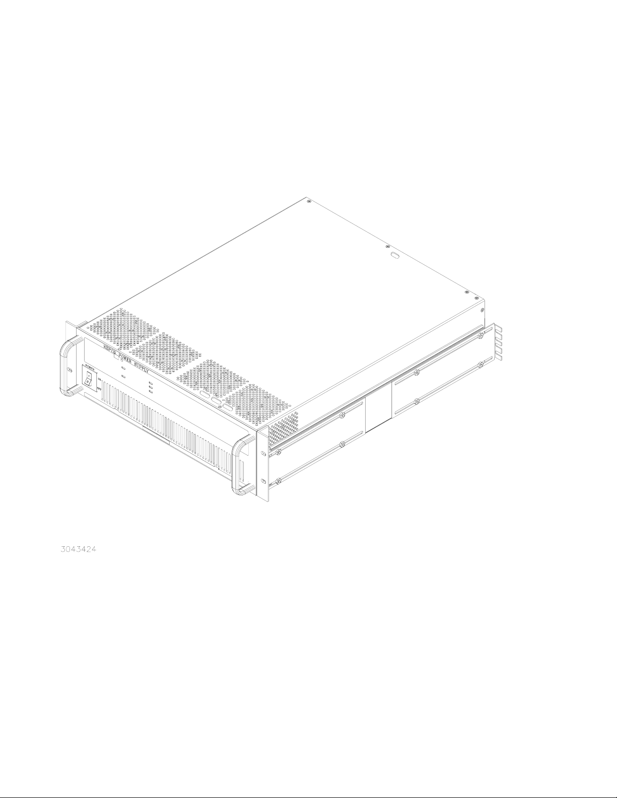
FIGURE 1-1. HIGH POWER BOP-GL SERIES POWER SUPPLY
x BOP-1K 022814
Page 19

1.1 SCOPE OF MANUAL
This manual contains instructions for the installation, operation and servicing of the BOP-GL
series of 1000 Watt rack-mounted, 4-quadrant bipolar, programmable, voltage and current stabilized d-c power supplies manufactured by Kepco, Inc., Flushing, New York, U.S.A.
1.2 GENERAL DESCRIPTION
The BOP-GL Series (Figure 1-1), are true 4-quadrant programmable voltage and current power
supplies, meaning they are capable of both sourcing and sinking power. The BOP-GL models
hereafter referred to as BOP, have been optimized for exceptionally low current ripple and noise
and improved stability (drift and temperature), making them ideal for driving inductive loads such
as large magnets or motors. These bipolar power supplies pass smoothly through zero without
switching to provide true ± voltage and ± current. These BOP power supplies use switch mode
technology for low dissipation. A bi-directional, isolating, a-c input power factor correcting (PFC)
circuit recuperates energy sunk from an active load and sends it back into the line to maintain
low dissipation.
These BOP power supplies can be controlled remotely by an analog ±10V input for the main
channel (voltage or current), and by a +1 to +10V input for the limit channels. They can also be
controlled through one of the standard digital interfaces (GPIB or RS 232) to set voltage and
current and the four protection limits (+voltage, –voltage, +current and –current.) Output voltage
and current can be remotely monitored via the analog monitor signals present at the rear panel
Analog I/O Port connector, or by using SCPI commands via either the RS 232 or GPIB ports.
SECTION 1 - INTRODUCTION
1.3 SPECIFICATIONS
Table 1-1 below indicates parameters that vary for different 1000 Watt BOP-GL models; Table 12 lists general specifications that apply to all 1000 Watt BOP-GL models.
TABLE 1-1. BOP-GL 1000 WATT MODEL PARAMETERS
Model
1000 WATT MODELS
BOP 10-100GL ±10V d-c ±100A d-c 1.0 10.0
BOP 20-50GL ±20V d-c ±50A d-c 2.0 5.0
BOP 50-20GL ±50V d-c ±20A d-c 5.0 2.0
NOTE: When connecting active loads, the steady-state voltage of the active load must not exceed the maximum
voltage rating of the BOP. Otherwise the overvoltage protection will shut down the power supply.
d-c Output Range Closed Loop Gain
E
O Max
I
O Max
Vol tag e
Channel
Current
Channel
BOP-1K-GL 022814 1-1
Page 20

TABLE 1-2. BOP GENERAL SPECIFICATIONS
SPECIFICATION RATING/DESCRIPTION CONDITION
INPUT CHARACTERISTICS
A-C Voltage nominal 230 Va-c
range 176 - 264 Va-c
Frequency nominal 50-60 Hz
range 47 - 63 Hz
Current 176 Va-c 9.5A maximum
264 Va-c 6.4A maximum
Power factor
Efficiency 65% minimum, when sourcing
Switching frequency 70 KHz PFC Stage, 5% tolerance
EMC Compliance EN61326-1 (1997) Class A equipment
EMC immunity to: ESD EN61000-4-2 Electrostatic discharge
EMC emissions Conducted EN61000-3-2 harmonics
Leakage current 3.5 mA 230V a-c, 60 Hz
Insulation coordination Input Installation Category II
Pollution degree 2
OUTPUT CHARACTERISTICS
Type of stabilizer Voltage-Current, 4 quadrant Switch mode
Switching frequency 100KHz Output Stage, 5% tolerance
Source adjustment
range
Sink adjustment range voltage -100% to +100% of rating 0 to 50 deg C. Recuperated energy is sent
(1) Output characteristics are for a single standalone unit.
Source 0.99 minimum
Sink 0.97 minimum
Radiated RF EN61000-4-3
EFT EN61000-4-4 Electrical fast transient/burst
Surges EN61000-4-5
Conducted RF EN61000-4-6
EN61000-3-3 fluctuation & flicker
Conducted EN55011/CISPR11 0.15 to 30 MHz
Radiated EN55011/CISPR11 30 to 1000 MHz
Overvoltage Category II
Output Installation Category II maximum 300V (500V for BOP 10-100GL)
Overvoltage Category II
(1)
voltage -100% to +100% of rating 0 to 50 deg C
current -100% to +100% of rating
current -100% to +100% of rating
Single phase, or between two phases of a 3phase system
nominal output power
for TN or TT power systems
isolation voltage between each output terminal and chassis ground.
back into line for general reuse.
1-2 BOP-1K-GL 022814
Page 21

TABLE 1-2. BOP GENERAL SPECIFICATIONS (Continued)
SPECIFICATION RATING/DESCRIPTION CONDITION
OUTPUT CHARACTERISTICS (Continued)
Analog Programming
accuracy
Analog Readback
Accuracy
Digital Programming
resolution / accuracy
Digital Readback
resolution / accuracy
Digital Sustain Output update rate 400 updates/sec voltage or current
Digital Readback measurement rate 5 ms
measurement array 64 samples voltage and current
rejection of line-
related ripple/noise
Voltage stabilization in
voltage mode (digital or
analog control)
time effect (drift) 0.01% of rating 0.5 through 8 hours
temperature effect 0.005%/deg C of rating 0 to 50 deg C
ripple and noise 0.03% of rating rms
Current stabilization in
current mode (digital or
analog control)
time effect (drift) 0.01% of rating 0.5 through 8 hours
temperature effect 0.005%/deg C of rating 0 to 50 deg C
ripple and noise 0.01% of rating rms
Voltage 0.01% of rating • Voltage and Current limit in Voltage Mode
Current Limit 0.1% of rating
Current 0.01% of rating
Voltage Limit 0.1% of rating (source)
0.2% of rating (sink)
Voltage 0.1% • The analog readback signal is 0V to ±10V
Current
0.1%
Voltage 14 bits / 0.05% Voltage and Current limit in Voltage Mode and
Current Limit 12 bits / 0.1%
Current 14 bits / 0.05%
Voltage Limit 12 bits / 0.1% (source), 0.2% (sink)
Voltage 16 bits / 0.05% main or limit channel
Current 16 bits / 0.05% main or limit channel
50, 60, 125Hz Digital readback (see PAR. B.9).
source effect 0.01% of rating min-max input voltage
load effect 0.02% of rating 0-100% load current
source effect 0.01% of rating min-max input voltage
load effect 0.02% of rating 0-100% load voltage
and Current and Voltage Limit in Current
Mode.
• The programming signal is 0V to ±10V for
0 to ±E
Onom
±I
(Current mode).
Onom
• The programming signal is +1V to +10V for
10% to 100% of all four limits (±voltage,
±current)
• Input impedance is 20KOhms for the main
channel (voltage or current)
• When the limit channels are not used, the
limits are clamped to 1% above the nominal values.
• The limit source must be able to sink a
maximum 0.15mA @ +1V programming
signal
for 0 to ± Nominal values for voltage and
current.
• Output impedance of the analog readback
signal is <0.1 Ohm
• The output current is maximum 5mA.
Current and Voltage Limit in Current Mode
(Voltage mode) or for 0 to
BOP-1K-GL 022814 1-3
Page 22

TABLE 1-2. BOP GENERAL SPECIFICATIONS (Continued)
SPECIFICATION RATING/DESCRIPTION CONDITION
OUTPUT CHARACTERISTICS (Continued)
O
O
NOM
NOM
(2)
or I
(4)(5)
(4)(5)
NOM
O
(3)
.
Error sensing 0.25V or 1% of voltage rating per
wire (whichever is less)
Transient recovery in
voltage mode
Output isolation voltage d-c or p-p 300V (500V for BOP 10-100GL) Output to chassis ground
Series operation Master/slave Maximum of 2 identical units.
Parallel operation
Output Protection
limiting
Output Stage Protection Output overvoltage/overcurrent
Input Stage Protection (PFC) Internal overvoltage, undervoltage,
Small signal
Bandwidth for main
channel (analog or
digital)
Rise/Fall time voltage channel 475
External limit channels update rate 100mS max Voltage or current, positive and negative limit
(2) Remote error sensing applies to the main voltage channel. Feedback for the ±voltage limit channels is supplied locally
from the power terminals. Consult factory for a remote sensing solution applicable to the voltage limit channels.
(3) With GND-NET to GND link installed: 0.55mA at 300V (0.91mA at 500V for BOP 10-100GL).
(4) Consult factory to configure more than two units in series or parallel (three units for BOP 10-100GL in parallel).
(5) For multiple unit configurations, automatic shutdown upon accidental removal of the cable at the Master PAR/SER IN
PROTECT PORT can be implemented with a simple internal modification. Consult factory for details.
maximum excursion 5% of nominal output nominal voltage, 50% load step
Recovery time 350
d-c leakage current 0.1mA @ 300V
(0.1mA @ 500V for BOP 10-100GL)
Analog Voltage and current limited in four quadrants, adjustable
Digital Voltage and current limited in four quadrants, adjustable between ±Internal minimum
E
Heatsink overtemperature,
switchers overcurrent
overcurrent, heat sink
overtemperature, fan inoperative
Input circuit breaker overcurrent Trips circuit breaker to shut off unit
voltage channel 1 KHz minimum Into nominal resistive load, 10% of rating
current channel 800 Hz minimum
µsec Return within 1% of set voltage
Master/slave Maximum of 2 identical units
between 10% and 101% of E
or I
MIN
O
(box) (see Figure 1-3) and ±1.01 E
MIN
O
µSec Into nominal resistive load, measured from 10
current channel 500
µSec Into short circuit, measured from 10 to 90%,
Above rated output voltage
GND-NET to GND link not installed.
(maximum of 3 for BOP 10-100GL)
or I
NOM
O
Triggers latched shutdown protection of the
output module and PFC stage. Recover by
cycling power off, then on.
Into short circuit, 10% of rating
to 90%, from 0 to ±100% of rating
from 0 to ±100% of rating
values
1-4 BOP-1K-GL 022814
Page 23

TABLE 1-2. BOP GENERAL SPECIFICATIONS (Continued)
SPECIFICATION RATING/DESCRIPTION CONDITION
PROGRAMMING CHARACTERISTICS
Analog I/O Port
(see Table 2-11)
External Protection Port
(Table 2-5)
Trigger Port (See Table 2-4)
Remote ON-OFF
(6)
(voltage or current)
Protection Limit
+Voltage, –Voltage
+Current, –Current
Output voltage and
current analog readback
External Shutdown Isolated input for shutdown of the
External Shutdown
External On-Off
(pin 2):
Main channel
channels:
Mode control Voltage: open circuit or TTL logic 1
Flag
Flag
STANDBY External Trigger Shutdown (Isolated
–10V to +10V Full range output, 20K Ohm input impedance
+1V to +10V 10% to 100% of Nominal Range. Input voltage
Current: short circuit or TTL logic 0
–10V to +10V For –100% to +100% of rating for output volt-
BOP (latched status)
Isolated output indicating
shutdown status
Isolated output indicating
output on (enabled) or off (disabled,
STANDBY) status
Operation of pin 2 is controlled by OUTP:CONT command (see Par. B.15).
Settings are STANDBY, HIGH, LOW, OFF. Either OFF or STANDBY is required if
using OUTP ON and OUTP OFF commands to control the output. This input can be
disabled (OFF), or set to BOP-MG functionality (STANDBY) (see Table 2-4).
input. Logic 0 or short-circuit causes
the output to go to STANDBY (off,
disabled) (latched status)
clamped to 12V through 1K ohms. Maximum
of 0.15mA input current at 1V input voltage.
±Voltage protection controllable in Current
Mode, ±Current protection limits controllable
in Voltage mode. Set at 1.01 x nominal rating
of main channel for voltage or current.
Available only when digitally activated or
through power-up setting.
age and current, 0.1 Ohm output impedance,
5mA max. load.
Pulse width: 100 microseconds min.
Action delay: 100 microseconds max
Restore operation by cycling input power.
Action delay: 100 microseconds max
Action delay: 200 milliseconds max
Pulse width: 100
Action delay: 200 mS max
Restore operation by sending OUTP ON command via remote interface.
µS min.
HIGH (default) Isolated Input for controlling output
status, on or off. High or open (not
connected), output is on (enabled).
When 0 volts or short circuit applied
to the pin, output is off (disabled)
LOW Isolated Input for controlling output
status, on or off. Logic 0 = output is
on (enabled); Logic 1 or open (not
connected) = output is off (disabled).
OFF Trigger port disabled. Inputs applied
to pin 2 have no effect.
External Trigger
Input (pin 4)
Remote
ON-OFF Input
External Trigger
Input
(6) Main channel can be controlled by either external analog signal or digital remote control. Consult factory if both analog
and digital control are required.
BOP-1K-GL 022814 1-5
Isolated input for trigger events Pulse width: 100
Isolated input for toggling the BOP
output between output OFF (output
disabled) and output ON (output
enabled)
Isolated input for trigger events Pulse width: 100 microseconds min.
Pulse width: 6 mS min for any guaranteed unit
response.
Action delay: 200 mS max
Pulse width: 6 mS min for any guaranteed unit
response.
Action delay: 200 mS max
µS min.
Action delay: 500
Action delay: 200 milliseconds max.
Logic 0 (or short circuit) for output off and
logic 1 (or open) for output on. This logic can
be reversed (see PAR. 3.3.2.1). This output
can also be disabled, or set to BOP-MG functionality (STANDBY) (see Table 2-4).
Action delay: 500 microseconds max
µS max
Page 24

TABLE 1-2. BOP GENERAL SPECIFICATIONS (Continued)
SPECIFICATION RATING/DESCRIPTION CONDITION
PROGRAMMING CHARACTERISTICS (Continued)
Digital control remote IEEE 488-2 (GPIB) and RS 232 SCPI
Status
Display
remote RS 485 (BITBUS) IEEE 1118, used for series and parallel config-
front panel Lights:
Unit Status: POWER / FAULT/LIMIT (lights green for Power OK, lights red for Fault,
lights orange for Limit).
Output Status: OUTPUT ON (lights green On, not lit for Off).
Mode of Operation: VOLTAGE/CURRENT (lights green for Voltage, lights yellow for
Current).
Control: DIGITAL CONTROL (lights green for Digital control, not lit for Analog control).
Type: MASTER/SLAVE (lights green for Standalone or Master, lights yellow for
Slave).
remote Output voltage and current read back on GPIB or RS 232 bus and on the analog
readback lines.
urations
FUNCTION GENERATOR CHARACTERISTICS (See PAR. 3.5.7)
Maximum number of waveforms 1 Lost when the unit is turned off, must be
saved on the host computer)
maximum number of points per basic waveform
Maximum number of segments or basic waveforms per waveform
Types of Basic waveforms Sine (Sinusoidal waveform)
Triangle (Triangular waveform)
Pos. Ramp (Ramp waveform)
Neg. Ramp (Sawtooth waveform)
Square (50% Duty Cycle Pulse)
Count (Number of repetitions) Range: 1 to 255
For Count = 0 the waveform is exe-
cuted indefinitely until stop com-
Waveform Parameters Type: Voltage or Current
3933
126 Or maximum number of points (whichever
Level (DC waveform)
mand is sent
Count: number
Initial/Repeating
comes first)
• The time interval for each segment
depends on the type of waveform: period
for ramp and square waveforms, period or
fraction of period for sine and triangular
waveforms and time interval for DC levels
• Waveforms that exceed the maximum
number of points are not executed and an
error message is generated.
See LIST:CURR:APPLY (PAR. B.56) for current waveforms, or LIST:VOLT:APPLY (PAR.
B.79) for voltage waveforms.
See LIST:COUNt command (PAR. ). When
the count is complete or the waveform is
stopped using the CURR:MODE FIX command (PAR. B.27) or VOLT:MODE FIX command (PAR. B.94) the output remains at last
output value. The BOP can also stop at the
end of a cycle by using the CURR:MODE
HALT or VOLT:MODE HALT command.
See LIST:CURR:APPLY (PAR. B.56) for current waveforms, or LIST:VOLT:APPLY (PAR.
B.79) for voltage waveforms).
• Type of waveform, voltage or current, can
be selected only for a new waveform and
consequently applies to all waveform segments.
• All segments except the last may be set to
run once (using the LIST:COUN:SKIP command) or per the Count setting.
1-6 BOP-1K-GL 022814
Page 25

TABLE 1-2. BOP GENERAL SPECIFICATIONS (Continued)
SPECIFICATION RATING/DESCRIPTION CONDITION
FUNCTION GENERATOR CHARACTERISTICS
Basic waveform parameters Sine: Frequency (Hz), Amplitude (Vp-p or Ap-p), Offset (Vd-c or Ad-c),
Start Phase (°), Stop Phase (°).
Triangular: Frequency (Hz), Amplitude (Vp-p or Ap-p), Offset (Vd-c or Ad-c), Start
Phase (°), Stop Phase (°).
Ramp (Pos. or Neg.): Frequency (Hz), Amplitude (Vp-p or Ap-p),
Offset (Vd-c or Ad-c).
Square: Frequency (Hz), Amplitude (Vp-p or Ap-p), Offset (Vd-c or Ad-c).
Level: Timing (sec), Amplitude (Vd-c or Ad-c).
• The start/stop phases are global parameters, applicable to all sine/ triangular
waveform segments. They are independent and can have any value between 0°
and 360°.
LIST command characteristics for “string” type
waveform
Maximum number of points
• For single (global) dwell time:
• For <126 different dwell times:
• For >126 different dwell times:
Dwell time range: 93usec to 34msec.
Dwell time resolution (increment):
0.751usec
(Continued)
Note: Dwell time list must match (balance) the
amplitude list.
5900 (high resolution)
3933
2950
Skip feature (a number of steps can
be skipped from the LIST at the first
run using LIST:COUN:SKIP.)
Able to synchronize a LIST command
with multiple BOP’s or other devices
using Trigger Port (see Table 2-4
NOTE).
Able to sample output voltage or current during LIST command execution (see Figures B-2 and B-3).
Frequency: Not applicable to Level
Range (Hz) 0.01 to 443 Sine, Triangle
0.02 to 532 ±Ramp
0.02 to 1000 Square
Programming Resolution (Hz) 0.01
Accuracy 1.5% of Frequency Sine, Triangle, Square, ±Ramp
Period (applicable to Level only)
Range (Seconds): 0.0005 TO 5.0000
Resolution: 0.0001
Accuracy: 1.5% of Time Duration
BOP-1K-GL 022814 1-7
Page 26

TABLE 1-2. BOP GENERAL SPECIFICATIONS (Continued)
SPECIFICATION RATING/DESCRIPTION CONDITION
FUNCTION GENERATOR CHARACTERISTICS (Continued)
Amplitude Range
Main Channel Voltage (Volts p-p) 0 to 2 x E
Current (Amperes
p-p)
Protection Limit Channel . Current, bipolar
(Amperes)
Voltage, bipolar
0 to 2 x I
0 to I
0 to E
(Volts)
O
O
O
NOM
O
NOM
NOM
NOM
Offset Voltage (Volts)
–E
Current (Amperes) –I
O
O
NOM
NOM
to +E
to +I
O
O
NOM
NOM
Amplitude Resolution (Programming)
Main Channel and Off-
set
Voltage (millivolts a-
c)
.35 Sine
(millivolts d-c) 1 Triangle, Square, ±Ramp, Level:
Current (milliamperes a-c) .35 Sine
(millivolts d-c) 1 Triangle, Square, ±Ramp, Level:
Protection Limit Channel . Current, bipolar
(Amperes)
Voltage, bipolar
0.1
0.1
(Volts)
Amplitude Accuracy
Main Channel
and Offset
Protection Limit Channel . Current 0.1% I
Distortion (THD-F, Total Harmonic Distortion
relative to the fundamental component)
Voltage 0.05% E
Current 0.05% I
Voltage 0.1% E
5% max. Sine
13% max. Triangle
O
O
O
O
NOM
NOM
NOM
NOM
70% max. ±Ramp
47% max. Square
Start/Stop Angle (Phase) Range 0 to 360° Sine, Triangle
Programming Resolution 0.01°
Accuracy Start Angle 1°
Stop Angle 1° @ 0.01Hz, to 16° @ 443 Hz Frequency dependent
Sine, Triangle, Square, ±Ramp
Sine, Triangle, Square, ±Ramp
(set once for all segments)
Applies to offset of sine, triangle, ±ramp, and
square waveforms and to Level waveform
Amplitude.
1-8 BOP-1K-GL 022814
Page 27

TABLE 1-2. BOP GENERAL SPECIFICATIONS (Continued)
SPECIFICATION RATING/DESCRIPTION CONDITION
SAVE/RECALL CHARACTERISTICS
Number of Locations 99
(See PAR. 3.5.7)
15 locations available to be implemented on
power-up
Parameters Saved or Recalled All parameters saved for power-up
Mode of operation Voltage, Current or External For External the operating mode is deter-
mined by signal at I/O Port; no signal selects
voltage mode (see PAR. 3.4.1).
Reference type Internal, External or
Main channel
External Reference Level
Internal, External or
Limit channel
Lesser Limit
Main Amplitude
(Internal)
0 to E
(internal or external)
O
NOM
or I
O
NOM
Main Channel:
Voltage (Volts) for Voltage mode,
Current (Amperes) for Current mode
Protection Limit Amplitude
(Internal)
E
O
1.01 E
MIN
O
or I
NOM
O
or I
MIN
O
to
NOM
Limit Channel, Positive and Negative
Voltage (Volts) for Current mode,
Current (Amperes) for Voltage mode
Output status ON or OFF
MISCELLANEOUS FEATURES
Digital Maximum/Minimum Settings
Protection Limit Channel
(maximum value, Internal)
Digital Self-test capabilities Serial Interface, Analog, Output Serial Interface test requires Loop Back Test
Digital Interface Settings Data Format SCPI
Digital Calibration Computer-assisted through GPIB or
Power-up Settings (top cover accessible
(see Table 2-2)
Protection Limit
Type
Main Channel 0 to E
Bipolar (default) or Independent
1.01 E
O
E
O
NOM
MIN
O
NOM
or I
or I
(default) Software limit to setting of main channel:
NOM
O
or I
to
MIN
O
(internal)
NOM
O
Output Status @ Reset ON or OFF (OFF = default)
Serial Baud Rate Off, 9600, 19200 (Off = default)
Device Clear SCPI (default) or MATE
XON/XOFF Enable (default) or Disable
Prompt Disable (default), Enable,
Enable with Echo
RS 232 bus
Allow the unit at power up to:
• Set Load type
• Set the GPIB address
• Set the system configuration for multiple units in series or parallel.
• Enable the analog programming input for main channel and for limit channels.
• Enable the control signal for the mode of operation, voltage or current.
• Set the unit with previously saved custom settings.
• Reset the unit to internal factory default settings, after which the desired power-up
settings must be configured.
Voltage (Volts) for Voltage mode,
Current (Amperes) for Current mode.
Software limit to setting of protection limit
channel:
Voltage (Volts) for Current mode
Current (Amperes) for Voltage mode
connector
Except analog Voltage Readback with local
manual calibration.
BOP-1K-GL 022814 1-9
Page 28

TABLE 1-2. BOP GENERAL SPECIFICATIONS (Continued)
SPECIFICATION RATING/DESCRIPTION CONDITION
GENERAL (ENVIRONMENTAL) CHARACTERISTICS
Temperature operating 0 to +50 deg C Full rated load
storage -20 to +85 deg C
Cooling Two internal fans intake from the front, exhaust to the rear
Humidity 0 to 95% RH non-condensing
Shock 20g. 11msec ±50% half sine non-operating
Vibration 5-10HZ: 10mm double amplitude 3 axes, non-operating
10-55HZ: 2g 3 axes, non-operating
Altitude sea level to 10,000 feet
Safety Certification a-c power UL 3101-1 and EN 6101-1 Pending
PHYSICAL CHARACTERISTICS
Dimensions English 5.25' X 19" X 21.5" H X W X D
metric 133.3mm X 482.6mm X 546.1mm H X W X D
Weight, 1000W models English 53 lbs
metric 24.1Kg
Connections Source power 3-pin IEC connector
Load connections Nickel-plated copper bus bars With 1/4-20 threaded standoff.
Sensing Output
Terminal Block
Analog I/O control
port
PAR/SER CTRL IN
port
PAR/SER CTRL OUT
port
PAR/SER PROT IN
port
PAR/SER PROT OUT
port
EXT PROT port 6-pin phone jack See Table 2-5
Primary digital port 24-pin GPIB connector IEEE 488 port - See Table 2-12
Secondary digital
ports
External Trigger 4-pin stereo audio phone jack See Table 2-4
7-pin terminal block Default: 3 links installed for local sensing and
ground network connected.
15-pin D female See Figure 2-1, Table 2-11.
8-pin mini DIN connector See Figure 2-1, Table 2-8.
4-pin mini DIN connector See Figure 2-1, Table 2-7
8-pin phone jack See Figure 2-1, Table 2-9
8-pin phone jack See Figure 2-1, Table 2-10
6-pin phone jack RS 232 port - See Table 2-6
5-pin mini DIN female connector IEEE 1118 port - See Table 2-3
1-10 BOP-1K-GL 022814
Page 29
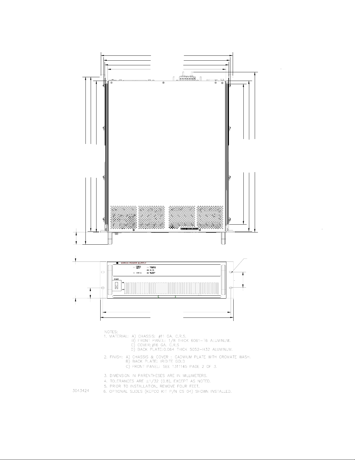
18.805 [477.63]
18.018 [457.64]
17.675 [448.93]
16.835 [427.60]
]
]
]
1
0
4
]
]
]
9
2
3
7
1
7
.
.
.
8
6
7
5
0
4
5
6
5
[
[
[
0
3
4
0
6
6
0
8
5
.
.
.
2
3
1
2
2
2
]
5
1
.
4
4
[
8
3
7
.
1
1
0
5
.
.
.
9
8
4
7
0
4
5
5
5
[
[
[
0
0
9
0
0
3
8
0
4
.
.
.
2
0
1
2
2
2
OBROUND 0.25x0.453 (4 LOC.)
]
4
5
.
2
3
1
[
8
1
2
.
5
]
4
3
.
7
3
[
0
7
4
.
1
18.235 [463.16]
18.985 [482.21]
]
7
2
.
6
5
[
5
1
2
.
2
FIGURE 1-2. BOP-GL POWER SUPPLY, OUTLINE DRAWING (SHEET 1 OF 2)
BOP-1K-GL 022814 1-11
Page 30
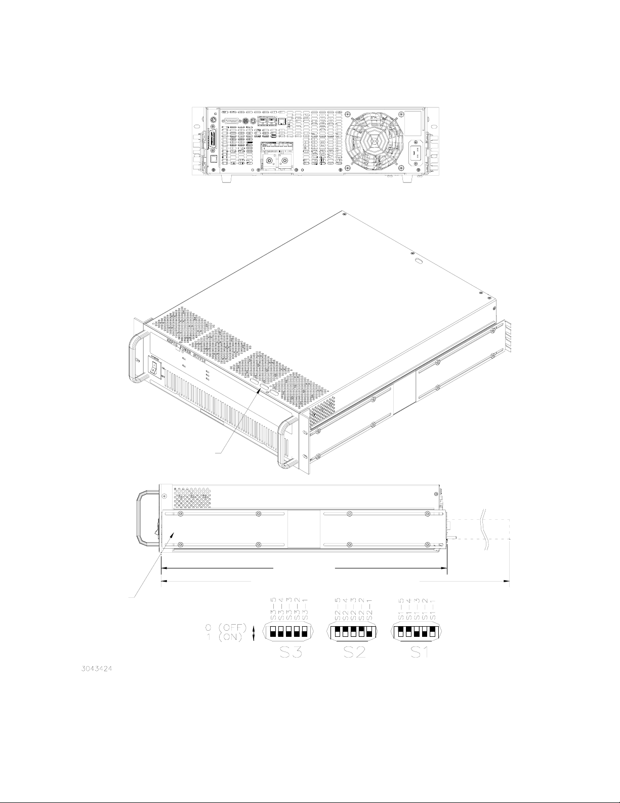
SEE DETAIL "A".
REAR VIEW
22.000 [558.79]
SLIDES TRAVEL DISTANCE: 23.000 [584.2]
SEE NOTE 6.
DETAIL "A"
FIGURE 1-2. BOP-GL POWER SUPPLY, OUTLINE DRAWING (SHEET 2 OF 2)
1-12 BOP-1K-GL 022814
Page 31

1.4 REMOTE CONTROL
The BOP Power Supply can be remotely controlled directly using either a) analog signal applied
to the Analog I/O Port (see PAR. 3.6 for details) or b) digital commands via either the IEEE
488.2 (GPIB) bus (see PARs. 3.6.3) or RS232C interface (see PAR.3.6.4) using IEEE 488 and
SCPI commands (see and Appendix A and B, respectively). The unit can be controlled with a
VISA (Virtual Instrumentation Software Architecture) driver to facilitate remote programming of
the BOP Power Supply (see PAR. 3.6.5). The VISA driver is an interface written in standard C
language which adds the proper SCPI syntax to commands sent to the BOP.
The BITBUS is used to allow communication between identical BOP units that are connected in
series or parallel to expand the voltage or current range (see PAR. 2.8).
1.5 FEATURES
1.5.1 DIGITAL CALIBRATION
The BOP Power Supply is digitally calibrated except for the zero and full scale settings of the
output voltage analog readback signal which are accessed through a cutout at the rear of the
top cover and are done manually. Digital calibration is done via the GPIB or RS 232 interface
using digital entries and a calibrated DVM, a precision d-c reference voltage source and precision shunt resistor. Previous calibration values are saved and can be restored if desired. The
original factory calibration values can also be restored. (Refer to Section 4.)
1.5.2 VOLTAGE/CURRENT PROTECTION
Positive and negative voltage or current protection values can be individually programmed.
Refer to PAR. 3.3.4.
1.5.3 WAVEFORMS
The BOP models have the capability to make the output follow complex waveforms. These may
be generated either using an analog reference voltage having the desired shape (see PAR.
1.5.6), or digitally using SCPI commands (see PAR. 3.5.7).
Digitally, the waveforms can be generated by specifying individual points in the waveform or
through the use of standard waveform segments. The segments provided by the BOP are, levels, positive and negative ramps, sine waves and triangle waves. While executing a waveform, it
is possible to cause other devices to be triggered by the BOP and for the BOP to wait for a trigger from another device. Segments or a series of points at the beginning of the waveform can
be programmed to be executed only once, or to be repeated as specified by the count. This
feature provides unique versatility for generating preconditions, resulting in a waveform that can
meet a variety of user requirements.
BOP-1K-GL 022814 1-13
Page 32

1.5.4 SAVING AND RECALLING SETTINGS
The BOP offers 99 memory locations that can be used to store a set of operating parameters for
later use. For each location, the user can store operating mode, output on/off, Main channel reference type and value, and protection reference type and value. The stored settings can then
be recalled to quickly program the unit to the predetermined setting. The settings stored in one
of the locations (1 to 15 only) can be programmed to be restored automatically upon power-up
using switch S3 (see Table. 2-2). Refer to PAR. 3.5.7 for further details.
1.5.5 EXTERNAL REFERENCE (ANALOG CONTROL)
An external reference, provided through the rear I/O analog port connector (see Table 2-11), can
be used to control the output of the BOP. The external reference can be attenuated by the digital
controls (see PAR. 3.4.1.2) so the unit operates with a lower amplification factor. In addition, the
BOP can limit its output based on the user-configurable limits so that, in the event of a failure in
the external reference, the devices connected to the output are protected. Refer to PAR. 3.3.10
for further details on using external signals to control the output.
1.5.6 EXTERNAL LIMITS
When the unit is controlled by an external reference, the protection limits can also be controlled
by analog signals that are digitally calibrated. The BOP samples the limit channel inputs and
applies the proper limit levels at variable rate (5 to 100 milliseconds), alternately sampling the
positive and negative limits. The external limit inputs are hardware-protected against overvoltage. Refer to PAR. 3.4.2
1.5.7 USER-DEFINED VOLTAGE/CURRENT MAXIMUM VALUES (SOFTWARE LIMITS)
The BOP output can be programmed not to exceed user-defined values. For example, the BOP
36-28GL, which has a maximum capacity of ±36V, ±28A, can be limited to +30V, –10V, +5A, -1A
for working with circuitry that might be damaged by higher levels. Once the limits are set, values
exceeding the limit values will not be accepted, including external references and protection limits. Refer to PAR. 3.3.5.
1.5.8 PARALLEL AND SERIES CONFIGURATIONS
Identical BOP units may be configured in series or parallel. If a series or parallel configuration is
enabled, communication between the master BOP and those configured as slave units occurs
via the BITBUS. Refer to PAR. 2.8 for further details.
1.5.9 ENERGY RECUPERATION
The BOP is a four-quadrant device as shown in Figure 1-3. Operating as a source, it delivers
energy into a passive load, and as a sink it operates as an electronic load, absorbing and dissipating energy from an active load. To minimize energy dissipation, the BOP employs energy
recuperation, where energy sinked from an active load is passed backwards through the output
circuit and the bidirectional input power factor correcting circuit to the a-c power lines, where it
becomes available for general reuse. This technology allows high power levels using switchmode technology while maintaining high efficiency and reduced size and weight.
1-14 BOP-1K-GL 022814
Page 33

1.6 EQUIPMENT SUPPLIED
Equipment supplied with the BOP power supply is listed in Table 1-3.
TABLE 1-3. EQUIPMENT SUPPLIED
ITEM FUNCTION
Source Power Entry mating connector Mates with source power entry connector 142-0381 (Kepco) (IEC 320)
PAR/SER CONTROL - IN
mating connector
Mating Connector, Trigger Mates with Trigger port. 142-0527 (Kepco)
Mating Connector, Analog I/O Port
(15-pin DSUB Connector)
Mates with PAR/SER CONTROL - IN port to allow
access to pins required for calibration
Mates with connector for Analog I/O port A2A5J6
Dsub 15 pin hood
Dsub 15 pin male
PART NUMBER
142-0488 (Kepco)
SP2501 (CUI Stack)
108-0374
(Tyco-Amp 207470-1)
142-0449
(Amphenol 17S-DA15P)
1.7 ACCESSORIES
Accessories for the BOP Power Supply are listed in Table 1-5.
1.8 SAFETY
Service must be referred to authorized personnel. Using the power supply in a manner not
specified by Kepco. Inc. may impair the protection provided by the power supply. Observe all
safety precautions noted throughout this manual (see listing on page E, preceding the Table of
Contents). Table 1-4 lists symbols used on the power supply or in this manual where applicable.
TABLE 1-4. SAFETY SYMBOLS
SYMBOL Meaning
WARNING! RISK OF ELECTRIC SHOCK!
CAUTION: REFER TO REFERENCED PROCEDURE.
!
WARNING
CAUTION
INDICATES THE POSSIBILITY OF BODILY INJURY
OR DEATH.
INDICATES THE POSSIBILITY OF EQUIPMENT
DAMAGE.
BOP-1K-GL 022814 1-15
Page 34

FIGURE 1-3. BOP OUTPUT CHARACTERISTICS
1-16 BOP-1K-GL 022814
Page 35

TABLE 1-5. ACCESSORIES
ITEM FUNCTION
PART NUMBER
Mating Connector, Trigger Mates with Trigger port. 142-0527 (Kepco)
SP2501 (CUI Stack)
IEEE 1118 (BITBUS)
Mating connector
Allows connection to IEEE 1118 (BITBUS) port. 142-0485 (Kepco)
KMDLA-5P (Kycon Inc.)
IEEE 488 Cable, (1 meter long) Connects BOP power supply to GPIB bus. SNC 488-1
IEEE 488 Cable, (2 meter long) Connects BOP power supply to GPIB bus. SNC 488-2
IEEE 488 Cable, (4 meter
Connects BOP power supply to GPIB bus. SNC 488-4
longs)
Interconnection Kit for multiple
identical power supplies in parallel (increase output current)
Interconnection Kit for multiple
identical power supplies in
series (increase output voltage)
Cables required to connect multiple BOP models in parallel for
increased current capability, e.g., connecting two BOP 1075GL models in parallel to produce a virtual BOP 10-150GL.
Cables required to connect multiple BOP models in series for
increased voltage capability, e.g., connecting two BOP 1075GL models in series to produce a virtual BOP 20-75GL.
KIT 219-0449 (2 in parallel)
KIT 219-0446
KIT 219-0447
KIT 219-0448
KIT 219-0443 (2 in series)
KIT 219-0444
(1)
(3 in parallel)
(1)
(4 in parallel)
(1)
(5 in parallel)
(1)
(3 in series)
Line Cord (250V, 20A) Provides connection to a-c mains via Nema 6-20P connector. 118-1087
Line Cord (250V, 20A) Provides connection to a-c mains via Nema L6-20P locking
118-1088
type connector.
RS 232 Cable Kit Contains RJ11 to RJ45 Patch cord, RJ 45 Patch cord, two RS
KIT 219-0436
232 adapters, one with male pins to connect to DTE equipment
and one with female pins to connect to a PC (personal computer), two RS 232 Loop Back test Connectors (one 6-pin and
one 8-pin) to test RS 232 communication and aid in isolating
RS 232 communication problems.
RS 232 Adapter (Male pins) Allows RS 232 port to be connected to DTE equipment. (Sup-
plied in KIT 219-0436.)
RS 232 Adapter (Female pins) Allows RS 232 port to be connected to a PC (personal com-
puter). (Supplied in KIT 219-0436.)
142-0487
(L-COM RA098M)
142-0506
(L-COM RA098F)
15-pin DSUB Connector Mating connector for Analog input connector A2A5J6
Dsub 15 pin hood
108-0374
(Tyco-Amp 207470-1)
Dsub 15 pin male
142-0449
(Amphenol 17S-DA15P)
IDC 6-pin connector Mating connector for RS-232 PORT, connector A1J5 and PRO-
TECT EXT. PORT, connector A2A5J7
IDC 8-pin plug Mating connector for PAR/SER PROTECT PORT (IN and
OUT) connectors.
Slides Allows easy withdrawal of unit from rack (see Figure 1-2).
142-0536
(Amphenol 5-555176-3)
142-0535
(Amphenol 5-557961-2)
CS 04
(Model CS 04 includes slides, brackets, all mounting hardware
and installation instructions.)
Heat Sink Provides adequate cooling for calibration sense resistors. 136-0451
Terminal Cover Protects against contact with output and barrier strip terminals.
129-0423
Install using the two existing screws (adjacent to two ground
terminals) securing rear panel to chassis. Particularly recommended for 72V and 100V models for safety purposes. Consult
factory for parallel/series configurations.
(1) Consult factory for configurations requiring more than two units in parallel or series
BOP-1K-GL 022814 1-17/(1-18 Blank)
Page 36

Page 37

SECTION 2 - INSTALLATION
2.1 UNPACKING AND INSPECTION
This instrument has been thoroughly inspected and tested prior to packing and is ready for
operation. After careful unpacking, inspect for shipping damage before attempting to operate.
Perform the preliminary operational check as outlined in PAR. 2.3. If any indication of damage is
found, file an immediate claim with the responsible transport service.
2.2 TERMINATIONS AND CONTROLS
a) Front Panel: Refer to Figure 3-1 and Table 3-1.
b) Rear Panel: Refer to Figure 2-1 and Table 2-1.
c) Top Cover: Refer to Figure 2-2 and Table 2-2.
FIGURE 2-1. BOP-GL SERIES REAR PANEL
BOP-1K-GL 022814 2-1
Page 38

TABLE 2-1. REAR PANEL CONNECTOR FUNCTIONS
NUMBER
(FIGURE 2-1)
1
2
3
4
5
6
7
8
9
10 terminals Frame or chassis terminals
11
12
13
CONNECTOR/TERMINAL
(REFERENCE DESIGNATOR)
IEEE 1118 (BITBUS)
PORT
(1)
(connector A1J4)
TRIGGER
(connector A1J3)
IEEE 488 (GPIB) PORT
(connector A1J6)
ANALOG I/O PORT
(connector A2A5J6)
PARALLEL/SERIAL
CONTROL PORT
(connectors A2A5J3, IN
and A2A5J4, OUT)
PARALLEL/SERIAL
PROTECT PORT
(connectors A2A5J1, IN
and A2A5J2 OUT)
EXT PROTECT PORT
(connector A2A5J7)
INPUT connector
(connector A7J1)
Monitor and Sensing
terminal block
(terminal block A7A1TB1)
COMMON
(terminal A7J3)
OUTPUT
(terminal A7J2)
RS232 PORT
(connector A1J5)
Used for multiple identical BOP master/slave parallel, and series and series-parallel
configurations (see Table 2-3).
May be used to initiate BOP output. (See Table 2-4.)
Used for Remote control of the BOP via the IEEE 488 (GPIB) interface (See Table
2-12.)
Provides interface for analog input/output signals. (See Table 2-11.)
Provides interconnections used to control parallel or serial configurations of identical BOP’s as a single power supply (see Table 2-8 for A2A5J3, IN and Table 2-7 for
A2A5J4, OUT).
Provides interconnections used to control protection shutdown of power supplies
connected in parallel or serial configurations (see Table 2-9 for A2A5J1, IN and
Table 2-10 for A2A5J2, OUT).
Provides means for controlling protection via external circuitry and provides status
flags to external circuitry. (See Table 2-5.)
Connects source power to unit.
Pin 1 - Line (or Line 1 without Neutral connection)
Pin 2 - Neutral (or Line 2 without Neutral connection)
Pin 3 - Ground (Protective conductor terminal)
Terminal block provides external connections as follows:
OUT S: Sense line connection to load (compensate for voltage drop on connections
to load.) (Terminal 2).
OUT MON: Monitor connection used to monitor output voltage at power terminals
and to implement local sensing (Terminal 3).
GND NET: Grounding network connection (Terminal 4).
GND: Chassis ground connection (Terminal 5).
COM MON: Monitor return connection (Terminal 6). Used to monitor output voltage
at power terminals and to implement local sensing.
COM S: Sense line return connection from load (Terminal 7)
Power output return from load.
Power output connection to load.
Used for Remote control of the BOP via the RS 232 serial interface. (See Table 2-6
for details.)
FUNCTION
2-2 BOP-1K-GL 022814
Page 39

SWITCH
(FIGURE
2-2)
S1
S2
VOLTAGE MONITOR
FULL SCALE ADJ
(A2A5R89)
VOLTAGE MONITOR
ZERO ADJ
A2A5R85
CALIBRATION
ADJUSTMENTS
S3
S2
S1
POWER-UP SETUP
SWITCHES
FIGURE 2-2. BOP-GL TOP COVER ACCESSIBLE COMPONENTS
TABLE 2-2. POWER-UP SETUP SWITCHES
SECTION FUNCTION DESCRIPTION
S1-1 Bit 1 (LSB) 1. Enable the GPIB address from 0 [00000] to 30 [11110]) while reading power-
S1-2 Bit 2
S1-3 Bit 3
S1-4 Bit 4
S1-5 Bit 5 (MSB)
S2-1
S2-2
S2-3
Master or Standalone (1)
Slave (0)
Series (1)
Parallel (0)
Bit 1 (LSB)
(see Table at right)
up switches S2 and S3 during a normal power-up (see PAR. 3.3.2.2 for
details).
2. Address 31 (11111) initiates a special power-up reset which resets the limits
to factory defaults (see PAR. B.143), allows selection of Load type, allows
selection of Remote on-off logic at Trigger port pin 2 and selection of RS 232
baud rate. (see PAR. 3.3.2.1 for details)
Establish whether the unit is standalone or designated as master or slave in a
multiunit series or parallel configuration
S2-5 S2-4
S2-3
(LSB)
Configure unit as
S2-1 = 1 S2-1 =0
0 0 0 Standalone N/A
0 0 1 Master with 1 slave Slave #1
01 0
Master with 2 slaves
(1)
Slave #2
(1)
S2-4
S2-5
Bit 2
(see Table at right)
Bit 3
(see Table at right)
01 1
10 0
Master with 3 slaves
Master with 4 slaves
(1)
(1)
Slave #3
Slave #4
NOTE: the unit will beep if the above switches are set to 110 or
111 (invalid setting). The unit will not beep if the switches are
set to 010, 011, 100, or 101 (2, 3, 4, or 5 slaves).
(1)
(1)
(1) Consult factory to implement configurations of more than one slave.
BOP-1K-GL 022814 2-3
Page 40

SWITCH
(FIGURE
2-2)
S3
TABLE 2-2. POWER-UP SETUP SWITCHES (CONTINUED)
SECTION FUNCTION DESCRIPTION
S3-1
(LSB)
S3-2
S3-3 S3-3 and S3-4 determine limits upon power-up:
S3-4
(MSB)
S3-5
Function established
by S3-5
Establish
function of
S3-1 through S3-4
S3-5 determines the function of S3-1 through S3-4:
S3-5 = 1: S3-1: Voltage mode (1) or Current mode (0)
S3-2: Analog Input ON (1) or Analog Input OFF (0) Analog
input ON enables pin 11 of the I/O port.
S3-4 S3-3 Description
00
01
10
11
S3-5 = 0: Setting S3-4 (MSB) through S3-1 (LSB) to 0 (off) [0000] estab-
lishes a special analog control configuration upon power-up:
Analog Input ON (main channel reference, pin 11 of Analog I/O
port enabled), limit channel references (pins 5, 6, 13 and 14 of
Analog I/O port) enabled and pin 2 of Analog I/O port enabled
(1 or open = voltage mode, 0 or short = current mode).
Analog External Protection limits enabled (see
PAR. 3.4.2)
Digital –V and –C Prot Max (Internal) set to
max. +V and +C Protect Max (Internal) set to
min. (box).
Digital +V and +C Prot Max (Internal) set to
max. –V and –C Prot Max (Internal) set to min.
(box).
Digital ±V Prot Max and ±C Prot Max (Internal)
set to max.
Setting S3-4 (MSB) through S3-1 (LSB) to 1 [0001] to 15
[1111], restores custom configuration previously saved in
selected location 1 to 15. (See PAR. 3.5.7)
TABLE 2-3. IEEE 1118 CONNECTOR INPUT/OUTPUT PIN ASSIGNMENTS
CONNECTOR PIN SIGNAL NAME FUNCTION
IEEE 1118, referenced to pins 5, 8
(2-Wire Differential Interface)
IEEE 1118, referenced to pins 1, 3
(2-Wire Differential Interface)
Connect to pin 5 or 8 to add an internal termination resistor
to first/last unit on the daisy chain.
IEEE 1118 (BITBUS)
PORT
(connector A1J4)
1, 3 (shorted) CONTROL BUS “A”
5, 8 (shorted) CONTROL BUS “B”
6TERMINATOR
2-4 BOP-1K-GL 022814
Page 41

TABLE 2-4. TRIGGER PORT PIN ASSIGNMENTS
CONNECTOR PIN SIGNAL NAME FUNCTION
1 LOGIC GND Return for EXT TRIGGER and REMOTE ON-OFF signals.
2 REMOTE ON-OFF Logic 0 or short-circuit referenced to logic GND (pin 1) sets
the output OFF (output disabled). Logic 1 (TTL or 5VCMOS) or open sets the output to ON (output enabled).
This logic can be reversed (see 3.3.2.1 for details.).
When using digital control this pin can also be a) disabled
to allow OUTP ON and OUTP OFF to control the output or
TRIGGER PORT
(connector A1J3)
3 NOT USED
4 EXT. TRIGGER INPUT Logic 0 for at least 100
b) configured to put the unit in standby (see PAR. B.15).
Logic 0 or short circuit for at least 100
output and puts the unit in standby, however Logic 1 (TTL
or 5V CMOS level) does NOT enable the output. A remote
OUTP ON command must be used to enable the output.
Response to this signal is relatively slow (200mS max).
µsec disables the
µsec or short-circuit referenced to
logic GND (pin 1) causes a trigger event. Logic 1 (TTL or
5V CMOS level) rearms the trigger feature. Response time
µsec max.
is 500
TABLE 2-5. EXTERNAL PROTECTION CONNECTOR INPUT/OUTPUT PIN ASSIGNMENTS
CONNECTOR PIN SIGNAL NAME FUNCTION
Cathode of LED optocoupler (through a 510 ohm resistor) which is
used for external isolated shutdown. Anode of LED is connected to
(A2A5J7) pin 2. A positive voltage (3.5 to 15V) at pin 2 (referenced to
1 SD_EXT_K
2 SD_EXT_A
EXT. PROTECT PORT
(connector A2A5J7)
NOTE: Upon receipt of LIST:SET:TRIG command (PAR B.72), the Output Off flag (EXT_C/EXT_E) no longer represents output on/
off state. Instead, this signal can be used to trigger an external device. The transistor state (conducting or not conducting)
and the pulse width duration is controlled by the LIST:SET:TRIG command. Upon receipt of LIST:CLE command (PAR
B.49) the Output Off flag reverts to representing output on/off status as described above.
3 PG_EXT_C
4 PG_EXT_E
5 EXT_C
6 EXT_E
pin 1) shuts down the unit. This signal shuts down unit functionality.
The unit remains powered, but no output is available and the front
panel POWER/FAULTLIMIT LED will turn red. Response is relatively
fast (100
cycle power off, then on.
Anode of LED optocoupler which is used for external isolated shutdown. (See pin 1 above.)
Collector of optocoupler-transistor which is used for external isolated
“power OK” flag. Transistor emitter is connected to (A2A5J7) pin 4.
When unit is operating normally, transistor is saturated. Current
through transistor should not exceed 5mA and supply voltage should
not exceed 15V.
Emitter of optocoupler-transistor which is used for external isolated
“power OK” flag. (See pin 3 above.)
Collector of optocoupler-transistor which is used for external isolated
“Output OFF” flag. Transistor emitter is connected to (A2A5J7) pin 6.
When output is OFF, transistor is saturated. Current through transistor should not exceed 3mA and supply voltage should not exceed
15V. See NOTE below for alternate function.
Emitter of optocoupler-transistor which is used for external isolated
“output OFF” flag. (See pin 5 above.)
µS max.). To resume normal operation it is necessary to
BOP-1K-GL 022814 2-5
Page 42

TABLE 2-6. RS232C PORT INPUT/OUTPUT PIN ASSIGNMENTS
CONNECTOR PIN SIGNAL NAME FUNCTION
1 RTS Request To Send (protocol not used)
2RXD Receive Data
RS 232
PORT
A1J5
3 TXD Transmit Data
4 LOGIC GND Logic Ground
5 LOGIC GND Logic Ground
6 CTS Clear To Send (protocol not used)
TABLE 2-7. PARALLEL/SERIAL CONTROL OUT PORT PIN ASSIGNMENTS
CONNECTOR PIN SIGNAL NAME FUNCTION
1 SGND Local signal ground
PAR ALLEL /SER IAL
CONTROL OUT
PORT
(A2A5J4)
2 No connection
S_IN_PARALLEL Relayed signal for daisy chain connection. (See PARALLEL/SERIAL IN
3
4 No connection
PORT (A2A5J3) pin 3)
TABLE 2-8. PARALLEL/SERIAL CONTROL IN PORT PIN ASSIGNMENTS
CONNECTOR PIN SIGNAL NAME FUNCTION
1 SGND Local signal ground
2 No connection
S_IN_PARALLEL Input for programming output current of a parallel-connected slave. Pro-
PAR ALLEL /SER IAL
CONTROL IN PORT
(A2A5J3)
3
4 No connection
5 No connection
IOUT_M_UNIT Output for programming slave current when the unit is a parallel-con-
6
7 No connection
S_IN_SERIAL Input for programming output voltage of a series-connected slave. Pro-
8
vided by master unit.
Level: –10V to +10V controls the current between –I
nected master
Level: –10V to +10V programs slave current to –I
vided by master unit or from previous slave if multiple slaves connected.
Level: –E
+E
Onom
Onom
to –E
to +E
Onom
controls programs output voltage from
Onom
.
Onom
Onom
to +I
to +I
Onom
Onom
.
.
2-6 BOP-1K-GL 022814
Page 43

TABLE 2-9. PARALLEL/SERIAL PROTECT IN PORT PIN ASSIGNMENTS
CONNECTOR PIN SIGNAL NAME FUNCTION
PARALLEL/SERIAL
PROTECT IN PORT
(A2A5J1)
SD_A Anode of LED optocoupler which is part of protection circuit for parallel
1
PGOUT_C Collector of optocoupler transistor which is part of protection circuit for
2
SD_RETURN Completes return connection for the protection circuit which receives
3
4 No connection
5 No connection
6 No connection
7 GND Local power ground.
ALLOW EXT_ERR Provides energy for the protection circuit (master unit only). Disabled at
8
or series combination. Cathode of LED is connected to PARALLEL/
SERIAL PROTECT OUT PORT (A2A5J2) pin 1 (see Table 2-10). When
activated, the optocoupler shuts down the unit. LEDs from all units of the
parallel or series combination are connected in series.
parallel or series combination. Transistor emitter is connected to PARALLEL/SERIAL PROTECT OUT PORT (A2A5J2) pin 2 (see Table 2-10).
When unit is operating normally, transistor is saturated. Transistors from
all units of the parallel or series combination are connected in series.
energy from the master unit.
power up to prevent shutdown during power up.
TABLE 2-10. PARALLEL/SERIAL PROTECT OUT PORT PIN ASSIGNMENTS
CONNECTOR PIN SIGNAL NAME FUNCTION
SD_K Cathode of LED optocoupler which is part of protection circuit for parallel
PARALLEL/SERIAL
PROTECT OUT
PORT
(A2A5J2)
1
PGOUT_E Emitter of optocoupler transistor which is part of protection circuit for
2
SD_RETURN Relayed connection, provides return for the protection circuit which
3
4 No connection
5 No connection
6 No connection
7 No connection
8 No connection
or series combination. (See IN port (A2A5J1) pin 1,Table 2-9.)
parallel or series combination. (See IN port (A2A5J1) pin 2,Table 2-9.)
receives energy from the master unit.
BOP-1K-GL 022814 2-7
Page 44

TABLE 2-11. ANALOG I/O PORT INPUT/OUTPUT PIN ASSIGNMENTS
CONNECTOR PIN SIGNAL NAME FUNCTION
CAUTION: it is recommended that source power of external equipment connected to the Analog
Port be applied through an isolating transformer to avoid ground loops or possible
damage to the BOP due to incorrect equipment a-c wiring (e.g., defeating of ground
connection).
1NC
External input signal, TTL logic referenced to pin 9, controls the mode
2VM-/CM
3 IOUT_DMM
4SGND
5 – I_LIM_EXT
ANALOG I/O
6 – V_LIM_EXT
PORT
A2A5J6
7NC
8NC
9 GND Ground - Used for VM-/CM (pin 2) return
10 SGND Signal Ground (used for EXT_REF (pin 11) return
11 E XT_R EF
12 GND1 Ground (Used for pin 5, 6, 13 and 14 return)
13 +I_LIM_EXT
14 +V_LIM_EXT
15 VOUT_DMM
NOTE: When disabled, the external limit channels are automatically set 20% higher than BOP nominal references.
of operation when using external reference (goes to the digital board
that changes VM-/CM signal). Logic 0 (or pin grounded) = current
mode, logic 1 (or pin not connected, the default) = voltage mode (see
PAR. 3.4.1).
Output analog signal referenced to pin 4 for monitoring output current,
0V to ± 10V corresponds to zero to ± full scale current.
Signal Ground used for IOUT_DMM (pin 3) and VOUT_DMM (pin 15)
return.
Analog input signal referenced to pin 12, 0V to +10V sets the negative
current limit between zero and –I
imum current (e.g., for BOP 36-28GL +10V sets negative current limit
, +10V corresponds to rated max-
Omax
to –28A) (see PAR. 3.4.2). Open = disabled (see NOTE).
Analog input signal, 0V to +10V, sets the negative voltage limit between
zero and –E
for BOP 36-28GL +10V sets negative voltage limit to –36V). Open =
, +10V corresponds to rated maximum voltage (e.g.,
Omax
disabled. (See PAR. 3.4.2.) Open = disabled (see NOTE).
External analog reference signal referenced to pin 10, used for main
channel (either voltage mode or current mode) to control BOP output
voltage or current. 0V to ±10V corresponds to zero to ± rated nominal
(full scale), voltage or current (see PAR. 3.4.1).
Analog input signal referenced to pin 12, 0V to +10V sets the positive
current limit between zero and I
mum current (e.g., for BOP 36-28GL +10V sets positive current limit to
; +10V corresponds to rated maxi-
Omax
+28A) (see PAR. 3.4.2). Open = disabled (see NOTE).
Analog input signal, 0V to +10V sets the positive voltage limit between
zero and E
, +10V corresponds to rated maximum voltage (e.g., for
Omax
BOP 36-28GL +10V sets positive current limit to +36V. Open = disabled. (See PAR. 3.4.2.) (see NOTE).
Analog output signal referenced to pin 4 for monitoring output voltage.
0V to ±10V corresponds to zero to ± full scale voltage (5mA max. load),
2-8 BOP-1K-GL 022814
Page 45

TABLE 2-12. IEEE 488 PORT INPUT/OUTPUT PIN ASSIGNMENTS
CONNECTOR PIN SIGNAL NAME FUNCTION
I01 I/O Line
I02 I/O Line
I03 I/O Line
I04 I/O Line
I05 I/O Line
I06 I/O Line
I07 I/O Line
I08 I/O Line
IEEE 488
PORT
J5
1D
2D
3D
4D
5 EOI End or Identify
6 DAV D ata Va l i d
7 NRFD Not Ready for Data
8 NDAC Not Data Accepted
9 IFC Interface Clear
10 SRQ Service Request
11 ATN Attention
12 SHIELD Shield
13 D
14 D
15 D
16 D
17 REN Remote Enable
18 GND Ground (signal common)
19 GND Ground (signal common)
20 GND Ground (signal common)
21 GND Ground (signal common)
22 GND Ground (signal common)
23 GND Ground (signal common)
24 LOGIC GND Logic Ground
2.3 PRELIMINARY OPERATIONAL CHECK
A simple operational check after unpacking and before equipment installation is advisable to
ascertain whether the power supply has suffered damage resulting from shipping.
Refer to Figures 2-1, 2-2 and 3-1 for location of operating controls and electrical connections.
Table 3-1 explain the functions of operating controls/indicators. Refer to PAR. 3.3 for a description of basic operating techniques.
2.3.1 PRELIMINARY OPERATIONAL CHECK USING ANALOG CONTROL
1. With POWER switch set to off position, verify that the power-up switches at the top cover are
set to the factory default positions shown in Figure 2-3. This establishes GPIB address 6,
standalone operation, Voltage mode, Analog Input enabled and internal ±current limits
enabled and set to maximum.
NOTE: The unit is shipped with load type set to Active (for inductive loads). If necessary, refer
to 3.3.7 for an explanation of load types and to PAR. 3.3.2.1 to change the load type.
The logic for Remote on/off input at pin 2 of the Trigger port is set to high (1) or open
circuit for output on, low (0) or short circuit for output off.
BOP-1K-GL 022814 2-9
Page 46

S1: 00110 = GPIB ADDRESS 6
S2: 00001 = STANDALONE
S3: 11111 = VOLTAGE MODE,
ANALOG INPUT ON
±V AND ±C PROTECT MAX SET
TO MAXIMUM
FIGURE 2-3. FACTORY DEFAULT POWER-UP SWITCH SETTINGS
2. Connect a twisted wire pair (either #24 or #22 AWG) to the mating connector for the Analog
I/O port pins 11 and 10. Connect +10V d-c ±0.1mV to pin 11, referenced to pin 10, then
install the mating connector on the Analog I/O port at the rear panel.
CAUTION: DO NOT repeatedly toggle the POWER circuit breaker/switch as this may
damage the unit.
3. Connect the power supply to source power (see PAR. 2.5.2). With no load connected, set
POWER switch to the ON position.
4. Each time the unit is turned on an internal self-test is performed. If the unit passes, it initializes with the power-up settings established in step 1 and the front panel POWER/FAULT/
LIMIT light is green (power good), the DIGITAL CONTROL light is not lit (analog input
enabled) and the VOLTAGE/CURRENT light is green (voltage mode), MASTER/SLAVE light
is green (standalone or master configuration) and the OUTPUT ON light is lit (output
enabled). If the front panel POWER/FAULT/LIMIT light is red, the unit has failed self-test;
contact Kepco for further instructions. If the unit beeps, or the MASTER/SLAVE or VOLTAGE/CURRENT light blinks, refer to PAR. 3.8 for troubleshooting.
5. Connect a digital voltmeter (DVM) (resolution and accuracy of 0.01% or better) to the OUT S
and COM S terminals at the rear panel terminal block.
6. Verify DVM voltage reading matches the nominal voltage of the unit within 0.01% of rated
maximum voltage.
2.3.2 PRELIMINARY OPERATIONAL CHECK USING DIGITAL CONTROL
1. With POWER switch set to off position, verify that the power-up switches at the top cover are
set to the factory default positions shown in Figure 2-3. This establishes GPIB address 6,
standalone operation, Voltage mode, Analog Input enabled and internal ±current limits
enabled and set to maximum.
2. Set Power-up switch S3-2 to 0 (off) to disable Analog Input.
NOTE: The unit is shipped with load type set to Active (for inductive loads). If necessary, refer
to 3.3.7 for an explanation of load types and to PAR. 3.3.2.1 to change the load type.
3. Connect a twisted wire pair (either #24 or #22 AWG) to the mating connector for the Analog
I/O port pins 11 and 4. Connect +10V d-c ±0.1mV to pin 11, referenced to pin 4., then install
the mating connector on the Analog I/O port at the rear panel.
4. Connect the GPIB or RS 232 cable coming from the host computer to the appropriate port
(GPIB or RS 232) at the BOP rear panel.
2-10 BOP-1K-GL 022814
Page 47

CAUTION: DO NOT repeatedly toggle the POWER circuit breaker/switch as this may
damage the unit.
5. Connect the power supply to source power (see PAR. 2.5.2). With no load connected, set
POWER switch to the ON position.
6. Each time the unit is turned on an internal self-test is performed. If the unit passes, it initializes with the power-up settings established in step 1 and the front panel POWER/FAULT/
LIMIT light is green (power good), the DIGITAL CONTROL light is not lit (analog input
enabled) and the VOLTAGE/CURRENT light is green (voltage mode), MASTER/SLAVE light
is green (standalone or master configuration) and the OUTPUT ON light is lit (output
enabled). If the front panel POWER/FAULT/LIMIT light is red, the unit has failed self-test;
contact Kepco for further instructions. If the unit beeps, or the MASTER/SLAVE or VOLTAGE/CURRENT light blinks, refer to PAR. 3.8 for troubleshooting.
7. Send the following SCPI commands:
*IDN? The unit responds with model number and serial number.
FUNC:MODE VOLT Puts the unit in Voltage Mode.
VOLT:MODE FIX Allows digital control of the output.
CURR:PROT:LIM xx xx is the nominal current rating of the unit.
VOLT yy yy is the nominal voltage rating of the unit.
OUTP ON Enables the output.
MEAS:VOLT? Measures output voltage and returns value to host computer.
8. Connect a digital voltmeter (DVM) (resolution and accuracy of 0.01% or better) to the
OUTPS and COMS terminals at the rear panel terminal block.
9. Verify DVM voltage reading matches the nominal voltage of the unit within 0.01% of rated
maximum voltage.
2.4 INSTALLATION
2.4.1 RACK MOUNTING
The unit is shipped with four feet attached to bottom of the unit which must be removed prior to
installation (see Figure 1-2). The BOP is designed to be rack mounted in a standard 19-inch
wide rack using the mounting ears (supplied) attached to the front panel (see Figure 1-2). Allow
a minimum of 1.0 in. (25.4 mm) in front of the unit to permit air intake necessary for proper cooling of the unit. CAUTION: The rack must provide support at the rear (within 6 inches of
the rear panel). Optional slides can also be used (see PAR. 2.4.2).
2.4.2 SLIDE INSTALLATION
Optional slides are available for rack mounting (see Table 1-5 and Figure 1-2).
BOP-1K-GL 022814 2-11
Page 48

2.5 WIRING INSTRUCTIONS
Interconnections between an a-c power source and a power supply, and between the power
supply and its load are as critical as the interface between other types of electronic equipment.
If optimum performance is expected, certain rules for the interconnection of source, power supply and load must be observed by the user. These rules are described in detail in the following
paragraphs.
CAUTION: When working with active loads, the voltage or current of the active load
must not exceed the maximum voltage or current rating of the BOP. Otherwise the overvoltage or overcurrent protection will shut down the power supply.
2.5.1 SAFETY GROUNDING
Local, national and international safety rules dictate the grounding of the metal cover and case
of any instrument connected to the a-c power source, when such grounding is an intrinsic part of
the safety aspect of the instrument. The ground terminal of the source power connector (Figure
2-1) is connected to the chassis and the instructions below suggest wiring methods which comply with these safety requirements; however, in the event that the specific installation for the
power system is different from the recommended wiring, it is the customer's responsibility to
ensure that all applicable electric codes for safety grounding requirements are met. As a precaution, always connect the stud marked at the rear panel to proper earth ground.
2.5.2 SOURCE POWER CONNECTIONS
Source power is connected to the power supply via three-wire input power using the source
power mating connector supplied (see Table 1-3). See Table 1-2 for source power specifications. This power supply operates from single phase a-c mains power (or between two phases
of 3-phase a-c mains power) over the specified voltage and frequency ranges (Table 1-2) without any need for range selection.
2.5.3 D-C OUTPUT GROUNDING
Connections between the power supply and the load and sensing connections may, despite all
precautions such as shielding, twisting of wire pairs, etc., be influenced by radiated noise, or
“noise pick-up”. To minimize the effects of this radiated noise the user should consider grounding one side of the power supply/load circuit. The success of d-c grounding requires careful
analysis of each specific application, however, this recommendation can only serve as a general
guideline.
One of the most important considerations in establishing a successful grounding scheme is to
avoid GROUND LOOPS. Ground loops are created when two or more points are grounded at
different physical locations along the output circuit. Due to the interconnection impedance
between the separated grounding points, a difference voltage and resultant current flow is
superimposed on the load. The effect of this ground loop can be anything from an undesirable
increase in output noise to disruption of power supply and/or load operation. The only way to
avoid ground loops is to ensure that the entire output/load circuit is fully isolated from ground,
and only then establish a single point along the output/load circuit as the single-wire ground
point.
The exact location of the “best” d-c ground point is entirely dependent upon the specific application, and its selection requires a combination of analysis, good judgement and some amount of
2-12 BOP-1K-GL 022814
Page 49

empirical testing. If there is a choice in selecting either the OUTPUT or COMMON output terminals of the power supply for the d-c ground point, both sides should be tried, and preference
given to the ground point producing the least noise. For single, isolated loads the d-c ground
point is often best located directly at one of the output terminals of the power supply; when
remote error sensing is employed, d-c ground may be established at the point of sense lead
attachment. In the specific case of an internally-grounded load, the d-c ground point is automatically established at the load.
The output and common terminals of BOP power supplies are d-c isolated (“floating”) from the
chassis in order to permit the user maximum flexibility in selecting the best single point ground
location. Care must be taken in measuring the ripple and noise at the power supply: measuring
devices which are a-c line operated can often introduce additional ripple and noise into the circuit.
There is, unfortunately, no “best” method for interconnecting the load and power supply. Individual applications, location and nature of the load require careful analysis in each case. Grounding a single point in the output circuit can be of great importance. It is hoped that the preceding
paragraphs will be of some assistance in most cases. For help in special applications or difficult
problems, consult directly with Kepco's Application Engineering Department.
2.5.3.1 GROUNDING NETWORK CONFIGURATION
When the output is floating there is a tendency for large changes in output voltage to affect the
digital programming section, possibly resulting in an erroneous output. Decoupling capacitors
from each of the two output terminals to the chassis via a terminal block link form a grounding
network. The grounding network is designed to reduce high frequency noise and ensure that the
digital programming section is not adversely affected by the dynamic swing of the output. The
power supply is shipped with the grounding network connected: a connection between terminals
TB1-4 (GND NET) and TB1-5 (GND). To disconnect the grounding network from the output,
remove the connection across TB1-4 and TB1-5.
2.5.4 POWER SUPPLY/LOAD INTERFACE
The general function of a voltage- or current-stabilized power supply is to deliver the rated output quantities to the connected load. The load may have any conceivable characteristic: it may
be fixed or variable, it may have predominantly resistive, capacitive or inductive parameters; it
may be located very close to the power supply output terminals or it may be a considerable distance away. The perfect interface between a power supply and its load would mean that the
specified performance at the output terminals would be transferred without impairment to any
load, regardless of electrical characteristics or proximity to each other.
The stabilized d-c power supply is definitely not an ideal voltage or current source, and practical
interfaces definitely fall short of the ideal. All voltage-stabilized power supplies have a finite
source impedance which increases with frequency, and all current-stabilized power supplies
have a finite shunt impedance which decreases with frequency. The method of interface
between the power supply output and the load must, therefore, take into account not only the
size with regard to minimum voltage drop, but the configuration with regard to minimizing the
impedance introduced by practical interconnection techniques (wire, bus bars, etc.). The series
inductance of the load wire must be as small as possible as compared to the source inductance
of the power supply: although the error sensing connection to the load compensates for the d-c
voltage drop in the power leads, it cannot compensate for the undesirable output effects of the
power lead inductance. These lead impedances (both power and sensing leads) are especially
important if the load: is constantly modulated or step-programmed; has primarily reactive char-
BOP-1K-GL 022814 2-13
Page 50

acteristics; or where the dynamic output response of the power supply is critical to load performance.
2.5.5 LOAD CONNECTION - GENERAL
Load connections require wires that are properly rated for the nominal output current of the unit.
Load connections to the BOP power supply are achieved via the OUTPUT and COMMON bus
bar-type terminals located on the rear panel. A barrier strip is provided at the rear panel for connection of the sense wires to the load (for remote sensing or multiple unit applications).
CAUTION: Never connect the load to the sense terminals. Monitoring instruments (e.g.,
DVM, etc.) are the only external equipment that may be safely connected to
the sense terminals.
CAUTION: Never connect the BOP OUTPUT terminal (or the load terminal tied to the
OUTPUT terminal) to earth-ground. Otherwise, if the controlling device is
grounded, the BOP can be damaged by the protection limit output current
flowing inside the BOP along the programming signal return path.
CAUTION: Do not connect both the load and the programming device return (common)
to earth-ground potential. Otherwise, If the COMMON power connection
between the BOP and the load is lost, then the BOP can be damaged by output current flowing inside the BOP along the programming signal return
path.
CAUTION: The safety features incorporated into the BOP to handle energy from Active
loads are unable to protect the power supply or the load if input power to the
BOP is lost or if the BOP Malfunctions. It is recommended that the user monitor “Power OK” flag pins 3 and 4 of the external Protect Port (see Table 2-5)
and implement a fast-acting means of disconnecting capacitive loads or
crowbarring inductive loads to prevent damage to both the BOP and the load
in the event of input power loss.
NOTE: Regardless of output configuration, either local or remote output sense lines
must be connected for operation.
1. Observe Polarities: The OUT S sensing wire must be connected to the OUTPUT
load wire, and the COM S sensing wire must be connected to the COMMON load wire.
2. If local sensing is used, install links (see Figure 2-4).
2.5.6 LOAD CONNECTION USING LOCAL SENSING
Figure 2-4 shows a typical configuration using local sensing and a grounded load; for local
sensing with an isolated (“floating”) load, do not install the ground connection (see Figure 2-4,
Note 2).
2.5.7 LOAD CONNECTION USING REMOTE SENSING
Figure 2-5 shows a typical configuration using remote sensing and a grounded load; for remote
sensing with an isolated (“floating”) load, do not install the ground connection (see Figure 2-5,
Note 2).
Use #22 AWG wire, twisted pair for remote sense connections.
2-14 BOP-1K-GL 022814
Page 51

2.6 COOLING
The power devices used within the power supply are maintained within their operating temperature range by means of internal heat sink assemblies and by two cooling fans. Periodic cleaning
of the power supply interior is recommended. Do not obstruct any vents on the unit. If the power
supply is located within a confined space, take care that the ambient temperature, which is the
temperature of the air immediately surrounding the power supply, does not rise above the specified limits (see Table 1-2).
2.7 SETTING UP THE UNIT
The following paragraphs describe the connections and initial BOP setup needed to operate in
the desired mode.
2.7.1 POWER-UP SETTINGS
The BOP uses three DIP switches (S1, S2, S3 shown in Figure 2-2 and explained in Table 2-2),
each with five segments to establish initial conditions upon power-up. These switches can be
configured for a) Reset Power-up or b) Normal Power-up.
Reset Power-up (PAR. 3.3.2.1) is used to change the load type (load type determines how the
unit responds to the output OFF command, see PAR. 3.3.7), logic of The Remote On/Off signal
at pin 2 of the Trigger port, and baud rate. Reset power-up also resets the limits to factory
defaults (see PAR. B.143). When using the unit on for the first time, refer to PAR. 3.3.2.1 to perform a Reset power-up.
Normal Power-up (PAR. 3.3.2.2) is used to establish the GPIB address, configure the unit as
either standalone or part of a multi-unit configuration, and establish how the unit is to be controlled (analog or digital), select operating mode (voltage or current), and select how protection
limits are to be controlled.
Refer to PAR. 3.2 for a summary of factory default settings established by the power-up
switches. The Reset Power-up (PAR. 3.3.2.1) must be used to change the load type, baud rate
or reverse the logic of Remote On/Off logic at Trigger port pin 2. Otherwise refer to PAR. 3.3.2.2
to establish normal power-up settings.
BOP-1K-GL 022814 2-15
Page 52

FIGURE 2-4. LOAD CONNECTIONS, LOCAL SENSING
GND
N / C OUT
OUT
MON
S
NET
GND
COM
MON
COM
S
FIGURE 2-5. LOAD CONNECTIONS, REMOTE SENSING
2-16 BOP-1K-GL 022814
Page 53

2.7.2 SETUP FOR ANALOG CONTROL
1. With power off configure the power-up setup switches (see Table 2-2 for details). Setup for
analog control can be accomplished through the power-up switches in one of two ways:
a. Setting S3-5 (MSB) through S3-1 (LSB) to 0 (off) [00000] is a unique configuration that
allows external signals applied to the I/O port to control the BOP upon power-up: Analog
Input ON (main channel reference, pin 11 of Analog I/O port) enabled, limit channel references (pins 5, 6, 13 and 14 of Analog I/O port) enabled, Voltage/Current mode is established by pin 2 of Analog I/O port (1 or open = voltage mode, 0 or short = current mode)
and output is set to ON (enabled).
b. Setting S3-5 to 1 allows S3-1 through S3-4 to determine how the unit is controlled.
• Set S3-1 to either 1 for Voltage mode or 0 for Current mode
• Set S3-2 to 1 to enable analog control (allow the main channel to be controlled by the
external reference applied to analog I/O Port pin 11).
• Set S3-3 and S3-4 to configure the protection limits (see Table 2-2).
2. Connect the load and programming and monitoring equipment as shown in Figure 2-6.
2.7.3 SETUP FOR DIGITAL CONTROL VIA GPIB
1. With all power off, connect the load to the BOP using either local or remote sensing. If units
are to be connected in series or parallel, refer to PAR. 2.8. Connect the GPIB connector to
the GPIB port (see Figure 2-1 and Table 2-1).
2. Refer to Table 2-2 and configure GPIB address, power-up settings, and master/slave status.
Set S3-5 to 1 and S3-2 to 0 to set Analog Input to OFF.
3. Refer to PAR. 3.3.2.2 to turn power on.
4. Refer to PAR. 3.3 for power supply basics and PAR. 3.6 for remote mode programming.
SCPI programming is described in PAR. 3.7; Appendices A and B provide syntax for SCPI
common and subsystem commands and queries implemented in this unit.
2.7.4 SETUP FOR DIGITAL CONTROL VIA RS 232C
1. With all power off, connect the load to the BOP using either local or remote sensing (refer to
PAR. 2.5).
2. If units are to be connected in series or parallel, refer to PAR. 2.8.
3. Connect the RS 232 connector to the RS 232 port (see Figure 2-1 and Table 2-1).
4. The default baud rate is 9600. The baud rate can be set to 19.2K by performing reset powerup (PAR. 3.3.2.1) with switch S3-1 set to 1.
5. Refer to PAR. 3.3.2.2 to turn power on.
Refer to PAR. 3.3 power supply basics and PAR. 3.7 for RS 232 operation. SCPI programming
is described in PAR. 3.7; Appendices A and B provide syntax for SCPI common and subsystem
commands and queries implemented in this unit. Refer to PAR. 3.6.4.3 to configure the RS 232
Port.
BOP-1K-GL 022814 2-17
Page 54

ANALOG
PROGRAMMING
SOURCE FOR
MAIN CHANNEL
ANALOG
PROGRAMMING
SOURCE FOR
PROTECTION
LIMIT CHANNELS
PROGRAMMING
SOURCE FOR
MODE CONTROL
VM
CM
ALTERNATIVE
MEANS OF
MODE CONTROL
H
0 TO ±10V
< 1Ω 20KΩ
L
SEE
WARNING
H1
+1 TO +10V
< 1
Ω
H2
0 TO 10V
L
SEE
WARNING
H
1.0mA
5mA
L
SEE
WARNING
TWISTED
TWISTED
100KΩ
ANALOG
I/O PORT
11
10
13
14
5
6
12
2
9
BOP-GL
POWER
SUPPLY
OUTPUT
TERMINALS
OUT
OUT MON
OUT S
COMM S
COMM MON
COMM
DVM
(OUTPUT
VOLTAGE
MEASUREMENT)
HL
LOAD
PRECISION
SHUNT
SEE
WARNING
VM
CM
LH
DVM
(OUTPUT
CURRENT
MEASUREMENT)
DVM
(OUTPUT
VOLTAGE
MONITOR)
DVM
(OUTPUT
CURRENT
MONITOR)
TWISTED
>1MΩ
TWISTED
>1MΩ
WARNING: IF THE LOAD IS GROUNDED, THE PROGRAMMING DEVICES AND THE MONITORING
INSTRUMENTS MUST BE FLOATING. IF THE LOAD IS FLOATING, THE PROGRAMMING
DEVICES AND MONITORING INSTRUMENTS CAN BE GROUNDED.
NOTE: USE AWG #24 OR AWG #22 WIRE FOR PROGRAMMING AND MONITORING/MEASURING
DEVICE INTERCONNECTIONS.
0 TO ±10V
<0.1Ω
<0.1Ω
0 TO ±10V
15
4
3
FIGURE 2-6. CONNECTIONS FOR ANALOG CONTROL AND MONITORING OF BOP-GL POWER SUPPLY.
2-18 BOP-1K-GL 022814
Page 55

2.8 MULTIPLE UNIT CONFIGURATIONS
Parallel and series configurations of identical BOP units increase the rated voltage and current
range of the power supply. Up to two units (three units for model BOP 10-100GL) can be connected in parallel to increase the current: I
= number of units in parallel. Similarly, up to two units can be connected in series to increase the
voltage: E
MAX (one unit)
x NS = E
MAX (parallel combination)
configurations requiring more than two units in series or parallel, contact Kepco. Multiple unit
configurations require the appropriate Interconnection Kit (see Table 1-5).
For all multiple unit configurations the master reports the system output parameters: voltage and
current; the slaves display and send to the master their own main channel parameter: voltage
for series configurations or current for parallel configurations.
Additional hex nuts are provided in the interconnection kit for sufficient cable separation so they
can be oriented as needed to fit onto the terminal.
NOTE: Multiple unit configurations require that all individual units be properly calibrated. (Units
shipped from Kepco have been factory-calibrated.) If not, refer to Section 4 to calibrate
the individual units prior to connecting them in parallel or series. Using calibrated units
ensures that the multiple unit configuration is calibrated; calibrating the multiple unit
configuration is neither needed nor possible.
2.8.1 MULTIPLE UNIT CONNECTIONS
MAX (one unit)
x NP = I
MAX (parallel combination)
where N
where NS = number of units in series. For
P
Before connecting the units in parallel or in series, turn off all units and remove any previous
interconnections between units as well as connections to the load
Refer to Table 2-2 and configure the top cover power up switches S1 through S3 of each unit for
the desired configuration master/slave, series/parallel (S2), GPIB address if desired (S1), and
additional settings (S3) as needed. Then turn on each unit for approximately 10 seconds to
allow the settings of S1, S2 and S3 to be stored.
Turn off the units, then proceed with the parallel or series connection. Figures 2-7 (local sensing) and 2-8 (remote sensing) show the connections for three parallel-connected units; Figures
2-9 (local sensing) and 2-10 (remote sensing) show the connections for three series-connected
units. These figures allow other configurations, e.g., two parallel- or series-connected units to be
easily deduced. Consult factory for configurations requiring more than two units in series or parallel (three units in parallel for BOP 10-100GL).
CAUTION: For both parallel and series configurations, remove links between (COM S)
and (COM OUT) terminals of all slaves to prevent damage to the unit and
maintain system accuracy. Make sure to accurately follow Figures 2-7
through 2-10 for proper connection of the units.
The following connections are required.
• Power cables
• Sense connections (either local or remote)
• Interconnection cables and terminations required for parallel or series configurations are
supplied in the applicable Interconnection Kit (see Table 1-5 for part number).
BOP-1K-GL 022814 2-19
Page 56

NOTE: Consult factory for configurations requiring more than two units in parallel.
FIGURE 2-7. PARALLEL CONFIGURATION, LOCAL SENSING, TYPICAL
2-20 BOP-1K-GL 022814
Page 57

NOTE: Consult factory for configurations requiring more than two units in parallel.
FIGURE 2-8. PARALLEL CONFIGURATION, REMOTE SENSING, TYPICAL
BOP-1K-GL 022814 2-21
Page 58

N / C OUT
N / C OUT
GND
OUT
NET
MON
S
GND
OUT
NET
MON
S
GND
GND
COM
MON
COM
MON
COM
COM
S
S
N / C OUT
NET
MON
S
GND
COM
MON
COM
S
GND
OUT
NOTE: Consult factory for configurations requiring more than two units in series.
FIGURE 2-9. SERIES CONFIGURATION, LOCAL SENSING, TYPICAL
2-22 BOP-1K-GL 022814
Page 59

N / C OUT
N / C OUT
GND
OUT
NET
MON
S
GND
OUT
NET
MON
S
GND
GND
COM
MON
COM
MON
COM
COM
S
S
N / C OUT
NET
MON
S
GND
COM
MON
COM
S
GND
OUT
NOTE: Consult factory for configurations requiring more than two units in series.
FIGURE 2-10. SERIES CONFIGURATION, REMOTE SENSING, TYPICAL
BOP-1K-GL 022814 2-23
Page 60

2.8.2 MULTIPLE UNIT SOURCE POWER
When multiple units are connected in series or parallel, the individual power supplies of the system may be connected to different phases of a 3-phase a-c power source.
2.8.3 MULTIPLE UNIT PROTECTION
For multiple unit configurations it is necessary to configure the protection so that a fault will shut
down all the interconnected power supplies. Figure 2-11 is a simplified diagram showing typical
protection interconnections for master/slave configurations. These interconnections are done
using the special cables and terminations supplied in the applicable Interconnection Kit available as an accessory (see Table 1-5).
FIGURE 2-11. TYPICAL MASTER/SLAVE PROTECTION INTERCONNECTIONS
Upon startup, PAR/SER PROT IN PORT pin 8 of the master goes low, and stays low until all
slaves are powered up. Normal power up of a unit causes the transistor connecting PAR/SER
PROT IN PORT pin 2 and PAR/SER PROT OUT PORT pin 2 to conduct. The transistors of all
units are connected in series, effectively shorting out all the shutdown diodes (the shutdown
diodes of all units are also connected in series) connecting PAR/SER PROT IN PORT pin 1 and
PAR/SER PROT OUT PORT pin 1. After all the units are powered up and operating normally,
the low at PAR/SER PROT IN PORT pin 8 changes to high, but the conducting transistors keep
the voltage at pin 8 low and the diodes are cut off. If a fault occurs, the transistor between PAR/
SER PROT IN PORT pin 2 and PAR/SER PROT OUT PORT pin 2 of the defective unit is cut off,
allowing current to flow through the shutdown diodes. This develops internal shutdown signals
that shut down all units.
2-24 BOP-1K-GL 022814
Page 61

2.8.4 OPERATING INSTRUCTIONS FOR MULTIPLE UNIT COMBINATIONS
1. Before either installing the units in a rack or stacking and connecting them one on top of the
other, configure the power-up settings as desired while the units are turned off.
a. For master unit, perform the Reset Power-up (see PAR. 3.3.2.1) to establish the load type,
logic for trigger port pin 2 (output on/off) and RS 232 baud rate (this also resets limits to
factory default settings (see PAR. B.143).
b. Configure the master/slave power-up switches (S2-1 through S2-5) for each unit per Table
2-2.
c. Configure the mode control power-up switches (S3-1 through S3-5). For analog control
refer to PAR. 2.7.2, for digital control via GPIB refer to PAR. 2.7.3 and for digital control via
RS 232 refer to PAR. 2.7.4.
NOTES: • It is not necessary to set power-up switch S3 segments for the slaves. Power-up
configuration is established automatically: mode of operation is established by the
series or parallel configuration switch S2-2 of each unit, the analog inputs are disabled, and the limit channels are set for maximum internal values
• After setting the power-up switches S1 through S3, turn on each unit for approximately 10 seconds to allow the unit to store the settings. Then turn off the units and
proceed to step 2.
2. Install the units in the rack, or stack them one on top of the other, then use the cables and
terminations supplied in the applicable Interconnection Kit (available as an accessory, see
Table 1-5) per Figures 2-7 through 2-10 as applicable. Figures 2-7 (local sensing) and 2-8
(remote sensing) show the connections for three parallel-connected units; Figures 2-9 (local
sensing) and 2-10 (remote sensing) show the connections for three series-connected units.
These figures allow other configurations, e.g., two parallel-connected units or two series connected units, etc. to be easily deduced.
CAUTION: For both parallel and series configurations, remove links between (COM S)
and (COM OUT) terminals of all slaves to prevent damage to the unit and
maintain system accuracy. Make sure to accurately follow Figures 2-7
through 2-10 for proper connection of the units.
3. Connect all units to a common a-c power source.
4. Connect the load to the master power output terminals using wires rated for the total current
and voltage of the system. For remote sensing use a twisted pair #22 AWG to connect OUT
S to OUT and COMM S to COMM at the load (see Figure 2-8 for parallel or Figure 2-10 for
series).
5. Connect monitoring/measuring devices to the master as shown in Figure 2-6.
6. Turn on all units, starting with the master. After the start-up sequence has ended, each unit
should not be beeping, the POWER/FAULT/LIMIT lights should be green, and the MASTER/
SLAVE lights should correctly identify master (green) and slaves (yellow).
BOP-1K-GL 022814 2-25
Page 62

7. If analog programming is to be used, connect the programming device to the master as
shown in Figure 2-6.
8. If analog control is to be used, the multiple unit combination is ready for use. Operation of the
multi-unit combination is identical to a standalone unit.
NOTE: When powering down the system, the master should be the last unit turned off.
9. If digital control is to be used, turn all units off.
a. Set power-up switch S3-2 to 0 (analog input disabled), Connect the GPIB or RS 232 cable
from the host computer to the GPIB or RS 232 port on the BOP, respectively.
b. Turn on all units, starting with the master. After the start-up sequence has completed, ver-
ify that
• all POWER/FAULT/LIMIT lights green,
• MASTER/SLAVE lights correctly indicate master (green) and slave(s) (yellow)
• It is recommended that the Output on-off pin at the Analog I/O port be disabled by sending OUTP:CONT OFF command to the master. This allows OUTP ON and OUTP OFF
commands to control the output digitally via the host computer. The DIG. CTRL light on
the master front panel will be on (green).
• All OUTPUT ON lights for the slaves are on (green). The master OUTPUT ON light status is determined by either the state of the signal at Trigger port pin 2 or an OUTP command (see PAR. 3.3.9 for details).
2.8.5 RESTORING A UNIT TO STANDALONE OPERATION
1. Turn off power to the master and all slaves.
2. Remove all interconnecting cables between units.
3. Perform steps a and b for each unit.
a. Access the power-up switches and reconfigure them as standalone (S2-1 set to 1, S2-2
through S2-5 set to 0)
b. Refer to PAR. 3.3.2.2 and reconfigure power-up switch S3 and S1 as desired.
c. After setting the power-up switches S1 through S3, turn on each unit for approximately 10
seconds to allow the unit to store the settings. Then turn off the unit and make connections
as desired.
2-26 BOP-1K-GL 022814
Page 63

3.1 GENERAL
This section explains how to operate the 1000 Watt BOP-GL Power Supply. The power supply
can be operated using either a) signals applied to the Analog I/O port control or b) digital commands via either the GPIB or RS 232 bus or c) a mixture of both.
Analog control (see PAR. 3.4) uses signals from the Analog I/O port to set the main channel
mode (voltage/current), control the output voltage or current, set protection limits, and uses a
signal applied to the Trigger port to control whether the output is on (enabled) or off (disabled).
Digital control (see PAR. 3.6) uses either the built-in GPIB (IEEE 488) (see PAR. 3.6.5) or RS
232 (see PAR. 3.7) interface to communicate with a remote computer. GPIB or RS 232 communication is via SCPI commands which afford full functionality of the BOP (see PAR. 3.7, Appendix A and Appendix B). Operation using digital control can be simplified by the use of the VISA
driver (see PAR. 3.6.5).
3.2 POWER-UP SETTINGS
CAUTION: Before connecting a load, note that the unit is will power-up with the configu-
ration set by the power-up switches accessible through the top cover (see
Table 2-2 for switch settings). Verify that these power-up settings are compatible with your load (see Figure 2-2 and Table 2-2 for switch settings).
SECTION 3 - OPERATION
To change to change load type, baud rate or Trigger port Remote on/off logic
refer to PAR. 3.3.2.1; to change all other power-up settings listed below refer
to PAR. 3.3.2.2.
In addition to the power-up settings determined by the switches accessed
through the top cover, many unit parameters may be saved for the next
power-up cycle using MEM:UPD commands (see PAR. B.12). When using
MEM:UPD, it is recommended that the unit be tagged with the custom powerup configuration to avoid unexpected behavior upon power-up.
Factory default power-up switch settings (Figure 2-3) are BOLD (other choices are in italics):
• Load type Active (Battery, Resistive)
• Trigger port pin 2 remote on/off logic set for:
logic 1 or open = output enabled, logic 0 or short = output disabled
(logic 0 = output enabled, logic 1 = output disabled)
NOTE: By using the OUTP:CONT command (see PAR. B.15), the Trigger port pin can be set
to put the unit in standby, or this input can be completely disabled if using OUTP command to control whether output is on or off.
• RS 232 Baud rate 9600 (19.2K)
• Standalone configuration (Master, Slave)
• Analog Control enabled (disabled)
BOP-1K-GL 022814 3-1
Page 64

• Vol tage mode (Current mode)
• internal control, ± limit values at max (1.01 x E
(internal control, +limit values at maximum (1.01 x E
–limit values at minimum (box))
(internal control, –limit values at maximum (1.01 x E
+limit values at minimum (box))
(External protection limits)
• GPIB address 6 (0 to 30)
All the above settings can be changed either by using the top cover-accessible switches while
power is off, or by sending SCPI commands if using digital control.
3.2.1 CHANGING THE DEFAULT POWER-UP SETTINGS
The default power-up settings listed in PAR. 3.2 can be changed as follows:
1. To change Load type, Trigger port pin 2 remote on-off logic or RS 232 baud rate, refer to
PAR. 3.3.2.1 for Reset Power-up.
2. To change all other power-up switch settings refer to PAR. 3.3.2.2 for normal power-up.
NOTE: All power-up settings can be changed by digital command, and if desired, the digitally
changed setting can be saved for power-up using the MEM:UPD command (see PAR.
B.12). However it is recommended that the unit be tagged with all settings saved for
power-up to avoid unexpected behavior upon power-up.
Onom
Onom
Onom
or I
or I
or I
Onom
Onom
Onom
)
),
),
3.3 POWER SUPPLY BASICS
The following paragraphs describe basic operation of the front panel controls and indicators
(PAR. 3.3.1), how to turn the unit on, including how to change the power-up defaults (PAR.
3.3.2), and an explanation of the basic techniques and principles needed to operate the power
supply.
When in Voltage mode, the power supply will (within the configured and rated limits) provide the
programmed output voltage. Current is determined by the load, and cannot exceed the Current
Protect limits. If the protect limit is reached, the POWER/FAULT/LIMIT LED light changes from
green (power OK) to orange.
When in Current mode, the power supply will (within the configured and rated limits) provide the
programmed output current. Voltage is determined by the load, and cannot exceed the Voltage
Protect limits. If the protect limit is reached, the POWER/FAULT/LIMIT LED light changes from
green (power OK) to orange.
3.3.1 CONTROLS AND INDICATORS
Refer to Table 3-1 and Figure 3-1 for a description of front panel controls and indicators.
3-2 BOP-1K-GL 022814
Page 65

FIGURE 3-1. BOP-GL SERIES FRONT PANEL
TABLE 3-1. FRONT PANEL CONTROLS AND INDICATORS
NUMBER
(FIGURE 3-1)
1
2
3
4
5
6
CONTROL/INDICATOR FUNCTION
POWER ON/OFF
circuit breaker A7CB1
OUTPUT ON LED
Unit Status
POWER/FAULT/LIMIT LED
Configuration Type
MASTER/SLAVE LED
Mode of Operation
VOLTAGE/CURRENT LED
DIG. CTRL LED Lights green for digital control, not lit for Analog Control.
Applies source power to unit.
Provides Output Status. Lights green for OUTPUT ON, not lit for output
off.
Lights green for POWER good, lights red for FAULT, lights orange for
LIMIT.
Lights green for MASTER or Standalone, lights yellow for SLAVE. For
multiunit configuration, this flashes (either green or yellow) to indicate unit
is a master, and is looking for slaves. If flashing continues, refer to PAR.
3.8 for troubleshooting.
Flashes during power-up while configuration is established. Lights green
for VOLTAGE mode, lights yellow for CURRENT mode. If flashing continues, refer to PAR. 3.8 for troubleshooting.
3.3.2 TURNING THE POWER SUPPLY ON
The status of the unit upon power-up depends on the configuration of the three power-up
switches (see Figure 2-2 and Table 2-2). Each power-up switch has five segments. For convenience the switch settings are often given for all segments as e.g., 00110 indicates segments 5,
4 and 1 are off (0) and segments 2 and 3 are on (1). In other instances a particular segment
(e.g., S3-5) is specified.
The reset power-up (PAR. 3.3.2.1) allows the power-up switches to establish 1) load type, 2)
Remote On/off logic at Trigger port pin 2 and 3) baud rate. The reset power-up also resets all
limits to the factory default condition (see PAR. B.143). The normal power-up (PAR. 3.3.2.2)
establishes the operating mode of the unit, whether control will be analog or digital, whether the
unit is standalone or part of a multi-unit configuration, and selects the GPIB address to be used
(see Table 2-2 for details).
BOP-1K-GL 022814 3-3
Page 66

3.3.2.1 RESET POWER-UP
At power up, if the GPIB address switches (S1) are set to all ones (address 31), the unit does a
reset power-up to establish the load type, baud rate and Remote On/Off logic of Trigger port pin
2. Reset power-up also causes the unit to reset all limits to the factory default configuration (see
PAR. B.143) and override limits saved by MEM:UPD LIM command. If load type, baud rate and
Trigger Port remote on/off logic do not need to be changed, refer to PAR. 3.3.2.2 for normal
power-up.
1. With power off before Reset Power-up power-up, at the top cover, set GPIB address to
11111 (switches S1-1 through S1-5 set to 1) and set all S3 switches to 0.
2. Set S3 as follows to establish the load type upon power-up: S3-2 to 1 = Resistive Load, S33 to 1 = Active Load, S3-4 to 1= Battery Load.
3. Set S3-1 to establish the baud rate for RS 232 operation: 1 = 19.2K, 0 = 9600.
4. Set S3-5 to 0 if desired to reverse the logic of the Remote On/Off signal at pin 2 of the External Trigger Port from the default (logic 1 = output enabled, logic 0 = output disabled) to logic
0 = output enabled, logic 1 = output disabled.
5. Do not change S2 settings.
CAUTION: DO NOT repeatedly toggle the circuit breaker/switch as this may damage the
unit.
6. Set POWER ON/OFF circuit breaker/switch (1, Figure 3-1) on front panel to ON. If actuator
does not lock when released, wait a few seconds before trying again. The circuit breaker is
“trip-free” design; if overload exists, contacts cannot be held closed by actuator.
7. The unit will begin beeping on and off at equal intervals. Set POWER ON/OFF circuit
breaker/switch on front panel to OFF and proceed to normal power-up (PAR. 3.3.2.2) to
complete power-up configuration.
For subsequent power-up, unless it is necessary to change RS 232 baud rate, load type, or the
logic at Trigger port pin 1, refer to PAR. 3.3.2.2 for normal power up (without resetting limits to
defaults).
3.3.2.2 NORMAL POWER-UP
Power-up conditions are established by switches S1, S2 and S3 available from the top cover
(see Table 2-2 and Figure 2-2). If either the load type upon power-up, RS 232 baud rate or the
remote on/off logic at Trigger Port pin 2 needs to be changed, refer to Reset Power-up setup,
PAR. 3.3.2.1. NOTE: Reset Power-up setup will reset the limits to factory default settings (overrides limit settings previously saved by MEM:UPD LIM command); Normal power-up leaves the
limits unchanged.
1. With power off set switches S1, S2 and S3 as desired in accordance with Table 2-2.
a. Set S3 to establish power-up conditions per Table 2-2: either a) use one of 15 previously
saved memory locations to establish power up conditions or b) Determine whether the
main channel will be controlled by an analog signal at I/O port pin 11 or by digital commands, establish main channel Mode (Voltage/Current) per PAR. 3.3.10) and establish the
protection limits (control of the limit channel) per par 3.3.11.
3-4 BOP-1K-GL 022814
Page 67

b. Set S2 to select standalone or multiple unit operation.
c. Set S1 with valid GPIB address from 0 to 30.
CAUTION: DO NOT repeatedly toggle the circuit breaker/switch as this may damage the
unit.
2. Set POWER ON/OFF circuit breaker/switch (1, Figure 3-1) on front panel to ON. If actuator
does not lock when released, wait a few seconds before trying again. The circuit breaker is
“trip-free” design; if overload exists, contacts cannot be held closed by actuator.
3. Unit performs self-test upon power-up initialization. If the unit passes self-test, the
POWER/FAULT/LIMIT light turns green and the unit is ready for operation; if it fails, the light
turns red.
3.3.3 VOLTAGE AND CURRENT PARAMETERS
Table 3-2 defines the voltage and current parameters used in this manual and provides references to the SCPI commands and queries associated with the parameter.
3.3.4 VOLTAGE/CURRENT PROTECT LIMITS (LIMIT CHANNEL SOFTWARE LIMITS)
These values are the references for the complementary channels: voltage in current mode and
current in voltage mode. The range for these values is between a minimum (box) value (see Figure 1-3) and 1% above the rated nominal value (see PAR. 3.3.5). If the unit is in voltage mode, it
will enter current protect mode when the load demands more current and energy than permitted
by the ±current protect settings. Similarly, if the unit is in current mode, it will enter voltage protect mode if the load demands more voltage and energy than permitted by the ±voltage protect
settings. When the protect settings are exceeded, the protection channel limits the output current or voltage, the POWER/FAULT/LIMIT LED lights orange (LIMIT), and the power supply
continues operation in the complementary mode of operation.
The BOP can be configured to program the protection limits as a single value that applies to
both protection channels using a common digital command, either CURR:PROT:LIM (see PAR.
B.37) or VOLT:PROT:LIM (see PAR. B.104) or by using or individual commands:
CURR:PROT:LIM:POS (see PAR. B.41), CURR:PROT:LIM:NEG (see PAR. B.39),
VOLT:PROT:LIM:POS (see PAR. B.108), VOLT:PROT:LIM:NEG (see PAR. B.106) to program
individual settings for positive and negative protection limits.
3.3.4.1 HIDDEN VOLTAGE AND CURRENT PROTECT LIMITS
The BOP employs two back-up channels which function as safety backups if a main channel
fails. The backup channel limits are fixed and not user accessible. These limits are set to 5%
over the nominal (rated) values for voltage or current. If the software limits for a main channel is
changed (PAR. 3.3.5), the corresponding protect channel limit is automatically changed to be
5% of the nominal (rated) value above the user-programmed software limit.
BOP-1K-GL 022814 3-5
Page 68

TABLE 3-2. VOLTAGE AND CURRENT PARAMETER DEFINITIONS
Term Definition
To m o dify
refer to
PAR.
+E
Onom
–E
Onom
+I
Onom
–I
Onom
+Voltage
–Voltage
+Voltage max
–Voltage min
+Current Protect
–Current Protect
+Current Protect Max
–Current Protect Min
Minimum (box)
+Current Protect Min
–Current Protect Max
The nominal (rated) output voltage of the unit determined by model; e.g. for
a BOP 36-28GL, ±E
Onom
is 36V.
The nominal (rated) output current of the unit determined by model; e.g. for
a BOP 36-28GL, ±I
Voltage mode only. Positive (+) and negative (–) output voltage values
Onom
is 28A.
established by remote command.
Range (+): 0 to +Voltage max
Range (–): 0 to –Voltage min
Voltage mode only. Maximum (positive) and minimum (maximum
negative) voltage that can be set.
Value (+): 0 to +E
Value (–): 0 to –E
Voltage mode only. Defines maximum (+) current and Minimum (maximum
Onom
Onom
negative) (–) that unit can source or sink.
Range (+): +Current Protect min to +Current Protect max
Range (–): –Current Protect max to –Current Protect min
Voltage mode only. Maximum setting for +Current Protect and Minimum
(maximum negative) setting for –Current Protect.
Value (+): +Current Protect min to (1.01 x +Current max)
Value (–): –Current Protect max to (1.01 x –Current min)
Voltage mode only. Minimum (positive) setting for +Current Protect and
maximum (maximum negative) setting for –Current Protect. Values of ±Current Protect between +Current Protect Min and –Current Protect Max (near
zero) are not allowed.This zone (also referred to as the
minimum (box) is
automatically calculated by the BOP (see Figure 1-3).
N/A
N/A
B.86
B.88, B.89,
B.90, B.92
B.29, B.30,
B.35, B.33
B.37, B.38,
B.41, B.39
N/A
+Voltage Protect
–Voltage Protect
Current mode only. Maximum positive (+) and minimum (maximum
negative) (–) voltage that can appear at the output.
Range (+): +Voltage Protect min to +Voltage Protect max
B.96, B.97,
B.102,
B.100
Range (–): –Voltage Protect max to –Voltage Protect min
+Voltage Protect Max
–Voltage Protect Min
Minimum (box)
+Voltage Protect Min
–Voltage Protect Max
Current mode only. Maximum (positive) setting for +Voltage Protect and
Minimum (maximum negative) setting for –Voltage Protect.
Value (+): +Voltage Protect min to (1.01 x +Voltage max)
Value (–): –Voltage Protect max to (1.01 x –Voltage min)
Current mode only. Minimum (positive) setting for +Voltage Protect and
maximum (maximum negative) setting for –Voltage Protect. Values of ±Voltage Protect between +Voltage Protect Min and –Voltage Protect Max (near
zero) are not allowed. This zone (also referred to as the
minimum (box) is
B.104,
B.105,
B.108,
B.106
N/A
automatically calculated by the BOP (see Figure 1-3).
+Current
–Current
Current mode only. Positive and negative output current established by
remote command.
B.19
Range (+): 0 to +Current max
Range (–): 0 to –Current min
+Current max
–Current min
Current mode only. Maximum (positive) and minimum (maximum
negative) current that can be set.
Value (+): 0 to +I
Value (–): 0 to –I
Onom
Onom
B.21, ,
B.25, B.22
3-6 BOP-1K-GL 022814
Page 69

3.3.5 MAXIMUM ACCEPTED VOLTAGE OR CURRENT (MAIN CHANNEL SOFTWARE LIMITS)
The software limits for the main channels (+Voltage Max, –Voltage Min, +Current Max and –
Current Min) are the maximum (positive) and minimum (Maximum negative) values allowable
for voltage and current. The default software limits are determined by the model: the nominal
(rated) values for voltage and current (e.g., 36V and 28A for the BOP 36-28GL). These four values can be adjusted independently. For example, a BOP 36-28GL, capable of delivering ±36V
in voltage mode can be configured to allow voltage to be adjusted only from –1V to +15V by
setting –Voltage Min to –1 and +Voltage Max to +15. To accomplish this via either GPIB or RS
232 ports send the following SCPI commands:
VOLT:LIM:POS 15 sets voltage positive limit to +15 volts
VOLT:LIM:NEG 1 sets voltage negative limit to 1 volt.
To ensure these settings are restored after a power cycle send MEM:UPD LIM and tag the
unit with the new power-up configuration. To restore factory default limits and undo the limits
saved by MEM:UPD LIM command, either perform a reset power-up (see PAR. 3.3.2.1) or
digitally query the limit(s), then digitally change them as needed, (if desired, save for powerup using MEM:UPD LIM). Tag the unit with new power-up settings.
Similarly, a BOP 36-28GL, capable of delivering ±28A in current mode can be configured to
allow current to be adjusted from –0.5A to +10A by setting –Current Min to –0.5 and +Current
Max to +10. Adjustment range is between 0 and E
for voltage and 0 and I
Onom
Onom
for current.
Note that these software limits are not the same as the Protect Limits described in PAR. 3.3.6.
To accomplish this via either GPIB or RS 232 ports send the following SCPI commands:
CURR:LIM:POS 10 Sets current max limit to 10 Amperes.
CURR:LIM:NEG 5 Sets current min limit to 0.5 Amperes.
To ensure these settings are restored after a power cycle send MEM:UPD LIM and tag the
unit with the new power-up configuration. To restore factory default limits and undo the limits
saved by MEM:UPD LIM command, either perform a reset power-up (see PAR. 3.3.2.1) or
digitally query the limit(s), then digitally change them as needed, (if desired, save for powerup using MEM:UPD LIM). Tag the unit with new power-up settings.
The main channel software limit values can be lowered (closer to zero) by the user, e.g., to prevent inadvertent damage to a specific circuit under test. When the maximum/minimum values
are lowered, the unit will not accept values that exceed the new software limits. The main channel software limits are always in effect, for both analog control and digital control. If the user
attempts to program a value that exceeds the software limit using a digital command, the command is considered invalid and is disregarded: a 120 error is produced. If analog control is
enabled, the output is clamped to the software limit for programmed values higher than the software limit.
If main channel software limits are changed from the default, the protection limits must
be changed to correspond to the new software limits (see PAR. 3.3.6). As an example,
changing +Voltage Max and –Voltage Min of a BOP 36-28GL to ±3V, respectively, causes the
unit to behave as if it was a BOP 3-28GL. In this case it is important to change the +V Protect
Max and –V Protect Min limits (e.g., to ±3.3V, respectively) so that the load is protected when
operating in Current Mode. This is done by sending the following command.
VOLT:PROT:LIM 3.3 This sets both limits to 3.3 volts.
BOP-1K-GL 022814 3-7
Page 70

To ensure these settings are restored after a power cycle send MEM:UPD LIM and tag the
unit with the new power-up configuration. To restore factory default limits and undo the limits
saved by MEM:UPD LIM command, perform a reset power-up (see PAR. 3.3.2.1).
3.3.6 MAXIMUM/MINIMUM PROTECTION LIMITS (SOFTWARE-CONTROLLED)
The ± protection limits are software limits that establish the maximum and minimum (maximum
negative) allowable levels of output voltage in current mode and current in voltage mode. The
default protection limits are 1% above E
Omax or
1% above I
Omax
.
CAUTION: WHEN WORKING WITH ACTIVE LOADS, ALWAYS ADJUST THE BOP PROTECTION LIMITS TO BE ABOVE THE MAXIMUM VALUES OF VOLTAGE OR CURRENT
EXPECTED FROM THE LOAD. FOR EXAMPLE, WHEN THE BOP IS OPERATING IN VOLTAGE MODE SINKING ENERGY FROM A CONSTANT CURRENT TYPE LOAD, SET THE
CURRENT PROTECTION LIMITS OF THE BOP ABOVE THE MAXIMUM CURRENT
EXPECTED FROM THE LOAD.
The protect channel limits are +V (voltage) Protect max, –V Protect min, +C (current) Protect
Max and –C Protect min (see Table 3-2); these prevent the unit from delivering voltage or current that exceed these settings. In voltage mode the current protect channel is clamped to the
limit value; in current mode the voltage protect channel is clamped to the limit value. Adjustment
range is between a minimum (box) value (see Figure 1-3) and 1% above the nominal (rated)
value.
3.3.7 DETERMINING HOW THE UNIT RESPONDS WHEN OUTPUT IS OFF (LOAD TYPE)
The BOP supports three Load Type selections (see Table 3-3) which determine how the power
supply responds when the output is off: ACTIVE, RESISTIVE and BATTERY. These selections
are designed to provide proper operation with different load types. It is important to note that the
Load Type selection does not affect the settings of the power supply for ON state; it only affects
the main internal reference level and the protection levels during the OFF state. Load type is
selected by performing a Reset Power-up (see PAR. 3.3.2.1) or by using the digital
OUTP:MODE command (see PAR. B.17).
WARNING
For inductive loads, and especially superconducting magnet type
loads, the inherent offset of the BOP in the OFF state may generate significant current in the circuit. A properly rated switch in parallel with a
resistor must be connected between the power supply and the load.
The switch must be open and voltage and current measurements at the
output must read 0V, 0A before removing or installing connections
between BOP and load.
ACTIVE. Active mode (default setting) is necessary for the power supply to function properly
and safely with inductive loads and constant-current-type active electronic loads. Active mode
can also be used with resistive loads. Table 3-3 indicates how the power supply responds to a
command to go from Output ON to OFF. When the output is disabled, the unit is set to voltage
3-8 BOP-1K-GL 022814
Page 71

mode, voltage is set to zero and both current protect and voltage limit are set to maximum.
When the unit is enabled, the pre-existing settings for voltage, current protect and voltage limit
are restored.
WARNING
For both inductive loads and constant-current-type active electronic
loads when the BOP output is set to OFF, a path is provided for absorbing either the energy accumulated in the reactance of the load during
the ON state, or energy delivered by an electronic load. This prevents
damage to the load and power supply as well as providing safety for
the user. However, In addition to the built-in safety features, constantcurrent-type active electronic loads must be adjusted to zero and voltage and current measurements at the output must read 0V, minimum
current, before handling the power supply-to-load connections.
RESISTIVE. This mode, as the name suggests, is useful for resistive loads. Table 3-3 indicates
how the power supply responds to a command to go from Output ON to OFF.
WARNING
Accessing the BOP after the output is disabled in BATTERY mode is
hazardous because (1) high current arcing is possible and (2) either the
external battery voltage, or the voltage (±Voltage Protection max) on
the BOP output terminals may be dangerous. Therefore, for battery and
constant-voltage-type active electronic loads it is recommended that
two properly rated external switches be installed for safety: one in
series with the battery, and one across the BOP output. After the unit is
set to OFF, first open the switch in series with the battery, then close
the switch across the BOP output to ensure safety before handling
BOP connections. When connecting the battery, the switch across the
output should be opened after the connections are complete and then
the switch in series with the battery should be closed. If the constantvoltage-type active electronic load is adjusted to zero before handling
the power supply-to-load connections, only the switch across the BOP
output is required.
BATTERY. This mode is necessary for the power supply to function properly and safely with
either battery or constant-voltage-type active electronic loads. This mode prevents the battery
from discharging during the OFF state. When the output is disabled (set to OFF), the BOP will
go to current mode, current will be set to zero, with voltage protect and current limit set to maximum. In this way the battery will not be discharged while the output is OFF. For constant-voltage-type active electronic loads this mode stops energy flow during the OFF state. Table 3-3
indicates how the power supply responds to a command to go from Output ON to OFF.
BOP-1K-GL 022814 3-9
Page 72

TABLE 3-3. POWER SUPPLY BEHAVIOR WHEN OUTPUT IS SET TO OFF
LOAD TYPE
SETTING
ACTIVE
RESISTIVE
BATTERY
If unit was in Voltage Mode when output OFF
command issued.
• Unit remains in voltage mode.
• Voltage set to zero.
• Both ± Current Protect set to maximum.
• Both ± Voltage Limit remain at maximum.
• Unit remains in voltage mode.
• Voltage set to zero.
• Both ± Current Protect set to minimum box values.
• Both ± Voltage Limit. remain at maximum.
• Unit set to current mode.
• Current set to zero.
• Both ± Voltage Protect. remain at maximum.
• Both ± Current Limit set to maximum.
3.3.8 EXTERNAL LIMITS
These limits are external analog signals which are converted within the BOP to digital signals
that program the protection channels only: current protect in voltage mode and voltage protect
in current mode. The range of each analog input signal is +1V to +10V, corresponding to a
range for clamping the output between minimum, 10% of nominal (positive and negative), to
+max/–min of nominal rating. Refer to PAR. 3.4.2 for details on implementing external limits.
Table 3-2 explains the effect that these limits have in both voltage and current mode, and references the corresponding paragraph for changing the parameter.
If unit was in Current Mode when output OFF
command issued.
• Unit set to voltage mode.
• Voltage set to zero.
• Both ± Current Protect remain at maximum.
• Both ± Voltage Limit set to maximum.
• Unit remains in current mode.
• Current set to zero.
• Both ± Current Protect set to minimum box values.
• Both ± Voltage Limit set to maximum,
• Unit remains in current mode,
• Current set to zero.
• Both ± Voltage Protect set to maximum.
• Both ± Current Limit remain at maximum.
3.3.9 ENABLING/DISABLING DC OUTPUT POWER
The behavior of the unit when disabled depends on the Load Type setting (see PAR. 3.5.5 and
Table 3-3 for details). There are four ways to disable the output:
1. Using Remote Shutdown pin 2 (referenced to pin 1) of the Protect Ext. port. This requires
the unit to be turned off, then on in order to restore operation (see PAR. 3.3.9.1).
2. Using Remote On-Off at pin 2 (referenced to pin 1) of the Trigger port which sets the output
to off (disabled) or on (enabled) by toggling a signal applied to the Trigger port (see PAR.
3.3.9.2)
3. Using Remote On-Off at pin 2 (referenced to pin 1) of the Trigger port to disable the output
and the digital command OUTP ON to enable the output (see PAR. 3.3.9.3).
4. Using digital commands OUTP OFF and OUTP ON to disable and enable the output (see
PAR. 3.3.9.4).
3-10 BOP-1K-GL 022814
Page 73

3.3.9.1 REMOTE SHUTDOWN
Functionality of a standalone unit can be shut down using a remote signal applied to the PROTECT EXT. PORT as shown in Figure 3-2 or 3-3. Functionality of a multiple unit configuration
(parallel, series or series-parallel) can be shut down by applying a remote signal to the master
PAR/SER PROTECTION PORT as shown in Figure 3-2 or 3-4. When the signal is momentarily
active (minimum 100 microseconds), power transfer between input and output is stopped (both
input and output internal modules are shut off). This condition is latched and shuts down unit
functionality. The unit remains powered, but no output is available and the front panel
POWER/FAULTLIMIT LED will turn red (fault). The unit must be powered off, then on again to
restore normal operation. This feature can be used a “panic” control or as an interlock shut
down for a system with other equipment.
For multiple unit configurations, automatic shutdown upon accidental removal of the cable at the
Master PAR/SER IN PROTECT PORT can be implemented with a simple internal modification.
Contact Kepco for details.
FIGURE 3-2. REMOTE SHUTDOWN USING EXTERNAL POWER, STANDALONE OR MULTIPLE UNITS
FIGURE 3-3. REMOTE SHUTDOWN USING INTERNAL POWER, STANDALONE UNITS
BOP-1K-GL 022814 3-11
Page 74

FIGURE 3-4. REMOTE SHUTDOWN USING INTERNAL POWER, MULTIPLE UNITS,
3.3.9.2 REMOTE ON-OFF USING TRIGGER PORT PIN 2
A standalone unit or a multiple unit configuration (parallel or series) can be set to output on
(enabled) or off (disabled) by applying a remote signal to the TRIGGER PORT as shown in Figure 3-5. For multiple unit configurations this signal must be applied to the master.
The factory default condition, established by the Reset Power-up configuration (see PAR.
3.3.2.1) is: when the signal is active (Logic 0 or short-circuit referenced to logic GND (pin 1), the
output is set to off after a maximum delay of 200 milliseconds and the front panel OUTPUT indicator goes off. Logic 1 (TTL or 5V-CMOS) or open sets the output to ON (output enabled) and
the OUTPUT indicator goes on.
This logic can be reversed so that logic 1 sets output off, logic 0 sets output on, by setting S3-5
to off (0) as directed during the Reset Power-up (PAR. 3.3.2.1).
3.3.9.3 REMOTE ON-OFF USING TRIGGER PORT (OFF) AND DIGITAL COMMAND (ON)
This method of controlling the output uses Trigger Port pin 2 to turn the output off, and the
OUTP ON command to turn the output on (see Figure 3-5). This method requires that
OUTP:CONT STANDBY (see PAR. B.15) be sent first. OUTP:CONT STANDBY allows a logic 0
(or short-circuit) pulse (100µS minimum) on pin 2 of the trigger port to turn off the output. A logic
1 or open circuit at Trigger port pin 2 has no effect on the output. Sending OUTP ON turns the
output on.
3.3.9.4 REMOTE ON-OFF USING DIGITAL COMMANDS
This method uses OUTP ON and OUTP OFF commands to control the output. This requires
that OUTP:CONT OFF command (see PAR. B.15) be sent first, disabling the Trigger port pin 2.
(If OUTP:CONT OFF is not sent, the state of Trigger port pin 2 will override the digital commands.) To save the OUTP:CONT state for power-up, send MEM:UPD INT and tag the unit with
the new power-up configuration
3-12 BOP-1K-GL 022814
Page 75

FIGURE 3-5. REMOTE ON-OFF, STANDALONE OR MULTIPLE UNITS
3.3.10 SETTING MAIN CHANNEL MODE (VOLTAGE OR CURRENT)
When the unit is turned on, the main channel mode is determined by the power-up switches.
• If S3 is set to 00000 the mode is determined by the status of pin 2 of the Analog I/O port
(see Table 2-11). Applying a TTL logic 1 (or open circuit) programs the unit to voltage
mode. Applying a TTL logic 0 (or short circuit) programs the unit to current mode.
• If S3 is set to 0nnnn (where nnnn = binary number from 1 (0001, where S3-1 = 1) to 15
(1111), unit turns on with the mode previously saved in the selected location, and may be
either voltage or current mode.
• If S3 is set to 1xxxn (xxx = set as desired; if n = 0, unit is set to current mode, if n = 1, unit
is set to voltage mode.
Once the unit is powered up, main channel mode can be controlled by the FUNC:MODE command (see PAR. B.45).
• Sending FUNC:MODE VOLT sets the unit to voltage mode and sending FUNC:MODE
CURR sets the unit to current mode.
• Sending FUNC:MODE EXT allows the mode to be determined by the status of pin 2 of
the Analog I/O port (see Table 2-11).
3.3.11 PROTECTION LIMITS
When the unit is turned on the protection limits are determined by the power-up switches:
• If S3 is set to 00000 the protection limits are controlled by the pins 5, 6, 13 and 14 of the
Analog I/O port (see Table 2-11).
• If S3 is set to 100xx (x = set as desired, S3-3 and S3-4 = 0, S3-5 = 1), the protection limits are controlled by the pins 5, 6, 13 and 14 of the Analog I/O port (see Table 2-11).
• If S3 is set to 0nnnn (where nnnn = binary number from 1 (0001, where S3-1 = 1) to 15
(1111), unit turns on with the limits previously saved in the selected location.
BOP-1K-GL 022814 3-13
Page 76

• If S3 is set to 101xx (x = set as desired, S3-3 = 1, S3-4 = 0, S3-5 = 1), –V Protect Max
and –C Protect Max are internally set to maximum (1.01 x nominal (rated) values. +V
Protect Max and +C Protect Max are Internally set to min. (box).
• If S3 is set to 110xx (x = set as desired, S3-3 = 0, S3-4 = 1, S3-5 = 1), +V Protect Max
and +C Protect Max are internally set to maximum (1.01 x nominal (rated) values. –V
Protect Max and –C Protect Max are Internally set to min. (box).
• If S3 is set to 111xx (x = set as desired, S3-3 = 1, S3-4 = 1, S3-5 = 1), ±V Protect Max
and ±C Protect Max are internally set to maximum (1.01 x nominal (rated) values.
Once the unit is powered up, main channel mode can be controlled by the CURR:PROT:MODE
(see PAR. B.31) and VOLT:PROT:MODE (see PAR. B.98) commands.
• Sending VOLT:PROT:MODE FIXED allows the voltage protect limits to be controlled by
VOLT:PROT:LIM commands and sending CURR:PROT:MODE FIXED allows the current
protect limits to be controlled by CURR:PROT:LIM commands
• Sending VOLT:PROT:MODE EXT allows the voltage protect limits to be controlled by
pins 6 and 14 of the Analog I/O port. Sending CURR:PROT:MODE EXT allows the current protect limits to be controlled by pins 5 and 13 of the Analog I/O port.
• Sending VOLT:PROT:MODE LESS allows the voltage protect limits to be controlled by
the lesser absolute value between that selected by the digital VOLT:PROT:LIM commands and the analog voltage on pins 6 and 14 of the Analog I/O port (see PAR. 3.4.2.1
for details).
• Sending CURR:PROT:MODE LESS allows the current protect limits to be controlled by
the lesser absolute value between that selected by the digital CURR:PROT:LIM commands and the analog voltage on pins 5 and 13 of the Analog I/O port (see PAR. 3.4.2.1
for details).
3.4 ANALOG REMOTE MODE PROGRAMMING
The recommended method for asserting Analog control requires that the unit be powered up
with power-up switches S3-1 through S3-5 set to 00000 (see Figure 2-2 and Table 2-2). This
sets up the following:
• The main channel is controlled by the external reference at pin 11 of the Analog I/O port
(see Table 2-11).
• The limit channels are controlled by the reference voltages at pins 5, 6, 13 and 14 of the
Analog I/O port (only two pins are active, determined by which limit channel is
active) (see Table 2-11).
• The mode (voltage/current) is determined by the state of pin 2 of the Analog I/O port
(see Table 2-11).
3-14 BOP-1K-GL 022814
Page 77

Pins of the Analog I/O port can also be used selectively to control the unit if the unit is powered
up with power-up switches S3-2 and S3-5 set to on (see Figure 2-2 and Table 2-2). This allows
the other S3 switches to selectively establish the following:
• Establish voltage or current mode (PAR. 3.3.10).
• Control the main channel using the BOP as a power amplifier (PAR. 3.4.1).
• Establish the protection limits (PAR. 3.4.2).
3.4.1 CONTROLLING THE OUTPUT USING THE BOP AS A POWER AMPLIFIER
The BOP can function as a power amplifier by means of the External Reference input at the
Analog I/O port. This analog signal controls the main channel of the BOP. To use the BOP as a
power amplifier see the following instructions for using the external reference for establishing
the maximum full scale output.: PAR. 3.4.1.1 for fixed gain, PAR. 3.4.1.2 for variable gain.
3.4.1.1 FIXED GAIN USING EXTERNAL REFERENCE CONTROL
The main channel of the BOP, voltage in voltage mode, and current in current mode, can be
controlled by an external reference voltage, 0 to ±10V applied at pin 11, referenced to pin 10, of
the Analog I/O port. The input impedance for this signal is 20K ohms.
NOTE: Power-up switch S3 must either be set to 00000 or S3-2 and S3-5 must be set to 1
(on) prior to power-up, otherwise the analog reference signal applied to Analog
I/O Port pin 11 will have no effect.
When the external reference is used, the BOP functions as a power amplifier, amplifying the
external reference at pin 11 to produce the output.
The nominal (inherent) voltage gain of each model is calculated by (G
and nominal (inherent) current gain is (G
between the nominal (rated) voltage or current (E
(E
) used to produce that output.
REF
So for an external reference of ±10V, the nominal voltage gain (G
NOM-I
) = I
Onom
Onom
/ E
. Thus the nominal gain is the ratio
REF
or I
), and the external reference
Onom
NOM-V
voltage gain of a BOP 36-28GL is 36/10 = 3.6. The nominal current gain (G
NOM-V
) = E
NOM-I
) = E
NOM-V
) is I
/ E
Onom
REF
/10, e.g., the
/10,
NOM-V
e.g., the current gain of a BOP 36-28GL is 28/10 = 2.8.
The external reference voltage may be d-c, a-c, or a combination of a-c plus d-c. The maximum
frequency of an a-c signal should be below the inherent frequency response of the BOP (1KHz
for voltage, 800Hz for current (see Table 1-2). For parallel or series combinations, the frequency
response is reduced as specified in the instruction manual included with the cable kit. A frequency that exceeds the bandwidth of the BOP will cause the output to be distorted.
For linear response (input vs. output) the software limit (see 3.3.5) should be set to nominal and
the maximum peak value (d-c plus a-c) of the reference signal must not exceed ±10V. If the
input signal exceeds the limit value (either ±10V if the software limit is set to nominal, or a lesser
voltage for a user-determined software limit) clipping of the output voltage or current to the limit
will occur.
NOTE: If the system limits have been modified (PAR. 3.3.5), the output of the power supply will
never exceed the modified system limits. E.g, for a BOP 36-28GL, if the system voltage
limit is modified to ±18V, applying a positive analog voltage to pin 11 that starts at zero
.
BOP-1K-GL 022814 3-15
Page 78

and rises to +10V causes the output to rise from zero and reach +18V when the external reference reaches +5V. The output stays at +18V while the reference increases
from +5V to +10V since the system voltage limits for this example are ±18V.
The command sequence that can be used is:
FUNC:MODE VOLT Sets unit to voltage mode.
VOLT:LIM 18 Sets main channel (voltage) software limits to ±18V.
CURR:PROT 20 Sets protection level to ±20A.
To restore all the above settings for power up, send *SAV3. This saves the settings to memory
location 3 (locations 1 through 15 can be used to establish initial power-up conditions). Set
power-up switch S3 to 00011 when performing a normal power-up (PAR. 3.3.2.2) to restore the
saved settings upon power up: main channel set to voltage, voltage limits set to ±18V and current protection set to ±18A.
The voltage limit setting can also be saved by sending MEM:UPD LIM (see PAR B.12) and tagging the unit with the new power-up settings. The factory default limits can be restored by performing a reset power-up (PAR. 3.3.2.1) which overrides the limits previously set by MEM:UPD
LIM.
NOTE: If the system limits have been modified (PAR. 3.3.5), the output of the power supply will
never exceed the modified system limits.
3.4.1.2 VARIABLE GAIN USING EXTERNAL REFERENCE LEVEL
The BOP can function as a variable gain power amplifier similar to the fixed (inherent or nominal) gain amplifier as described in PAR. 3.4.1.1. The user can determine a new (lower) full scale
output value for the ±10V reference level (applied at pin 11, referenced to pin 10, of the Analog
I/O port) by configuring the Reference input as follows:
NOTE: Power-up switch S3 must either be set to 00000 or S3-2 and S3-5 must be set to 1
(on) prior to power-up, otherwise the analog reference signal applied to Analog
I/O Port pin 11 will have no effect.
For an external reference of ±10V, the nominal voltage gain (G
) of a BOP 36-28GL is
NOM-V
36/10 = 3.6. If the new full scale voltage for 10V is set to 29V, the voltage gain is changed from
3.6 to 29/10 = 2.9. The gain can be changed only using digital CURR:MODE (see PAR. B.27)
and VOLT:MODE (see PAR. B.94) commands, but the output is controlled by the external reference signal.
Once the feature is configured, the new full scale value is entered by changing the active setting
value of the main channel. This determines the full scale output to be produced by a 10V external reference. The command sequence that can be used is:
FUNC:MODE VOLT Sets unit to voltage mode.
VOLT:MODE GAIN Enables gain mode of operation.
VOLT 29 For 10V at Analog I/O pin 11, output level set to 29V.
CURR:PROT 28.3 Sets protection level to maximum.
To restore the above settings for power up, send *SAV1. This saves the settings to memory
location 1 (locations 1 through 15 can be used to establish initial power-up conditions). Set
power-up switch S3 to 00001 when performing a normal power-up (PAR. 3.3.2.2) to restore the
3-16 BOP-1K-GL 022814
Page 79

saved settings upon power up: output set to voltage (gain) mode of operation with gain set to
2.9.
The gain in voltage mode is G
= V
V
entered at the front panel.
The gain in current mode is G
A
Amperes) entered at the front panel.
NOTE: If the system limits have been modified (PAR. 3.3.5), the output of the power supply will
never exceed the modified system limits.
3.4.2 EXTERNAL PROTECTION LIMITS
External protection limits are established upon power-up by switches S3-3 and S3-4. Once the
unit is powered up, the signals at the analog I/O port and the digital commands can be used to
control the protection limits. Refer to Table 2-2 and PAR 3.3.11 for details. The following paragraphs explain the operation of the analog signals assuming that they have been enabled.
Only two of the four LIM_EXT signals are active at a time, affecting the complementary protect
channel: ±current protect limit for voltage mode and ±voltage protect limit for current mode. A
voltage between +1V and +10V at the following pins (referenced to Ground, pin 12) will control
the corresponding protection parameter between 10% of the nominal value (see Figure 1-3) and
the corresponding positive or negative nominal full scale value.
• –I_LIM_EXT (pin 5) - This +1V to +10V analog signal sets the negative current protect
limit from 10% of the nominal value to –full scale current. +10V corresponds to rated
minimum (maximum negative) current (e.g., for BOP 36-28GL, +10V sets negative current limit to –28A).
/10 where V
SET
= I
SET
SET
/10 where I
is the desired full scale voltage (in Volts)
is the desired full scale current (in
SET
• –V_LIM_EXT (pin 6) - This +1V to +10V analog signal sets the negative voltage protect
limit from 10% of the nominal value to –full scale voltage. +10V corresponds to rated
minimum (maximum negative) voltage (e.g., for BOP 36-28GL, +10V sets negative voltage limit to –36V).
• +I_LIM_EXT (pin 13) - This +1V to +10V analog signal sets the positive current protect
limit from 10% of the nominal value to full scale current. +10V corresponds to rated maximum current (e.g., for BOP 36-28GL, +10V sets positive current limit to +28A).
• +V_LIM_EXT (pin 14) - This +1V to +10V analog signal sets the positive voltage protect
limit from 10% of the nominal value to full scale voltage. +10V corresponds to rated maximum voltage (e.g., for BOP 36-28GL, +10V sets positive voltage limit to +36V).
The maximum frequency of an a-c signal used for the external protection limit must be at least
10 times lower that the sampling rate of the external signal (10Hz), resulting in a bandwidth of
1Hz.
The external programming circuit must be able to sink 0.15mA maximum provided by the BOP.
When the input is an open circuit, the corresponding input signal automatically goes to 20%
above the nominal protection limit, but internally the protection value is clamped to 1.01 of nominal.
BOP-1K-GL 022814 3-17
Page 80

3.4.2.1 USING LESSER OF DIGITAL VS. ANALOG (EXTERNAL) LIMITS
The BOP provides the ability to automatically choose the lesser absolute value between the
external limits (applied to Analog I/O port pins 5, 6, 13 and 14) and the limits established by a
digital command. This feature is accessible through digital control and can be restored upon
power-up using a saved location.
For example, with a BOP 50-20GL, the maximum limit value in current mode can be set to 20V
using the digital interface, but the limits can be controlled by the analog limit signals applied to
pins 6 and 14 of the analog I/O port. However, if the signals at pins 6 or 14 exceed 4V (10V = full
scale or 50V, 4V is 2/5 of full scale = 20V), the digital limit will take effect and prevent the limit
from exceeding 20V. To implement this send the following commands:
VOLT:PROT 10 Sets the positive and negative protection to 10 volts.
VOLT:PROT:MODE LESS Allows protect limit to be automatically selected from either 1)
the external analog voltage applied to the Analog I/O port or 2)
10V set by VOLT:PROT 10. Whichever limit has a lower absolute value (closest to zero) has effect.
FUNC:MODE CURR Sets the output to current mode.
CURR:MODE EXT Sets main channel (current channel) to use an external level
applied to the Analog I/O port.
To restore the above settings for power up, send *SAV2. This saves the settings to memory
location 2 (locations 1 through 15 can be used to establish initial power-up conditions). Set
power-up switch S3 to 00010 to (S3-2 to 1) when performing a normal power-up (PAR. 3.3.2.2)
to restore the saved settings from location 2 upon power up: Current mode, External limits
enabled, limit to be the lesser of 10V (digital) or external limit signals applied to Analog I/O port.
3.4.3 MONITORING OUTPUT CURRENT USING AN ANALOG SIGNAL
The BOP provides output analog signals which are always available, 0 to ±10V, proportional to
the output current and voltage. The current monitor signal is available at pin 3, referenced to pin
4, of the Analog I/O port. The voltage monitor signal is available at pin 15, referenced to pin 4, of
the Analog I/O port.
3.5 DIGITAL CONTROL
3.5.1 PASSWORD PROTECTION
The Password is only effective when using digital control. The commands that can be password
protected are SYST:SEC:IMM and all CALibration commands. When the unit is shipped, the
password is set to DEFAULT. Refer to PAR B.139 to set a new password.
Before performing calibration or sending SYS:SEC:IMM, first send SYST:PASS:CEN (see PAR
B.137). When calibration is complete or when SYST:SEC:IMM has been executed, it is recommended that the password state be disabled using SYST:PASS:CDIS (see PAR B.138).
3.5.2 SETTING OPERATING MODE (VOLTAGE OR CURRENT)
The BOP uses two separate channels, one to set output voltage or current and one to set the
corresponding protection limit. When using digital control, the main channel is determined by
the FUNC:MODE command which selects either Voltage mode or Current mode, or allows the
status of Analog I/O port pin 2 to determine the mode (see PAR. 3.3.10 for details). The limit
3-18 BOP-1K-GL 022814
Page 81

channel is determined automatically by the main channel selected. When Voltage mode is
selected, the current protection limit channel is active, and when Current mode is selected, the
Voltage protection limit channel is active.
3.5.3 PROGRAMMING VOLTAGE OR CURRENT AND ASSOCIATED PROTECT LIMITS
When the operating mode is Voltage mode, use the VOLT command (see PAR. B.86) where
<exp_value> = digits with decimal point and Exponent, e.g., 2.71E1 for 27.1. For example, send
VOLT 2.71E1 to set output voltage to 27.1 Volts in voltage mode.
When the operating mode is Current mode use the CURR command (see PAR. B.86) where
<exp_value> = digits with decimal point and Exponent, e.g., 5.2-E1 for 0.52. For example, send
CURR 5.2-E1 to set output current to 0.52A in current mode.
3.5.4 PROGRAMMING ASSOCIATED PROTECT LIMITS
3.5.4.1 WHEN OPERATING IN VOLTAGE MODE
When the operating mode is Voltage mode, the following parameters are in effect (see Table 3-2
for definitions): +Voltage Max, –Voltage Min, +C Protect Max, +C Protect Min, –C Protect Max, –
C Protect Min, ±C Protect.
+Voltage Max and –Voltage Min are programmed using the VOLT:LIM commands (see PAR’s.
B.88 through B.93 for details). These commands limit the maximum ±voltage that can appear at
the output.
+C Protect Min and –C Protect Max cannot be programmed and are automatically set to minimum (box).
+C Protect Max and –C Protect Min. are programmed using the CURR:PROT:LIM commands
(see PAR’s. B.37 through B.42 for details.) These commands define the maximum values that
±current protection (±C Protect) can be set to. If the programmed values are exceeded, a command error -201, “Current range error” occurs.
+C Protect and –C Protect are programmed using the CURR:PROT commands (see PAR’s.
B.29 through B.36 for details.) These commands program the ±current protection values. If load
current reaches the ±current protection values, current will be clamped so ±current protection
values cannot be exceeded.
3.5.4.2 WHEN OPERATING IN CURRENT MODE
When the operating mode is Current mode, the following parameters are in effect (see Table 32 for definitions): +Current Max, –Current Min, +V Protect Max, +V Protect Min, –V Protect Max,
–V Protect Min, ±V Protect.
+Current Max and –Current Min are programmed using the CURR:LIM commands (see PAR’s.
B.88 through B.93 for details). These commands limit the maximum ±current that can appear at
the output.
+V Protect Min and –V Protect Max cannot be programmed and are automatically set to minimum (box).
+V Protect Max and –V Protect Min. are programmed using the VOLT:PROT:LIM commands
(see PAR’s. B.37 through B.42 for details.) These commands define the maximum values that
BOP-1K-GL 022814 3-19
Page 82

±voltage protection (±V Protect) can be set to. If the programmed values are exceeded, a command error -201, Voltage Range error” occurs.
+V Protect and –V Protect are programmed using the VOLT:PROT commands (see PAR’s. B.29
through B.36 for details.) These commands program the ±voltage protection values. If load voltage reaches the ±voltage protection values, voltage will be clamped so ±voltage protection values cannot be exceeded.
3.5.5 PROGRAMMING TECHNIQUES TO OPTIMIZE PERFORMANCE
3.5.5.1 PROGRAMMING VOLTAGE/CURRENT LIMIT AND CURRENT/VOLTAGE LIMIT
Kepco's auto-crossover digital supplies can operate in either voltage mode with current limit, or
current mode with voltage limit. The operating mode is determined by the voltage and current
commands received, as well as the load. Each time voltage and current commands are
received, the unit will go to the corresponding mode (voltage or current) with either the main
channel or the limit channel in control of the output (voltage or current), depending on the load
value. Each time there is a potential mode change, there is always an uncontrolled period of a
few fractions of milliseconds while the two feedback loops compete for control of the output. By
changing only the active parameter (e.g., voltage for voltage mode), there is no doubt as to what
the operating mode will be, so the unit is never uncontrolled, response is quick and no transients
are possible. Recommended programming techniques are:
1. Minimize programmed mode (voltage or current) changes. Unless absolutely required by the
test parameters, allow the power supply to automatically switch modes as determined by the
load. This will improve response time and reduce undesirable transients.
2. Once the mode (voltage or current) is programmed, program the active parameter to zero
and the complementary limit parameter to the maximum anticipated for application. Then
program only the active parameter. The active parameter is the parameter that controls the
output, e.g., voltage controls the output in voltage mode.
3. Never program both the active and complementary limit parameter to zero. This can result in
long response times. Set the active parameter to zero and the complementary limit parameter to a minimum, e.g., 10% of maximum, to ensure that the active mode is defined.
3.5.5.2 MAKING SURE THE PREVIOUS COMMAND IS COMPLETE
Some SCPI commands require a flash memory update and can take an indeterminate amount
of time to complete. These commands are:
•*SAV
• MEM:PACK
• MEM:UPD
•CAL:COPY
•CAL:SAVE
• SYST:PASS:NEW
• SYST:SEC:IMM
When sending these commands via the GPIB, these commands require a query to be added to
the command string to verify the previous command is complete. When the command is complete, the unit updates the status byte and indicates MAV (Message Available, bit 4 - see Table
A-3) is true. MAV indicates that there is a response to be received by the computer, so when it
3-20 BOP-1K-GL 022814
Page 83

becomes set, the unit is ready for its next command after reading back the data from the query
that was added to the command string.
When sending the above commands via the RS 232 bus, data flow control must be enabled
(XON) for the unit to properly update flash memory.
The *OPC? query is ideal to check if the previous command is complete since it returns either a
1 or 0. It is important that it be sent as a part of the same string as the command that causes a
flash update. As an example, sending CAL:SAVE 12/31/2005;:*opc? or *opc?;:CAL:SAVE
12/31/2005 are valid command strings. Sensing the commands separately will not verify that the
previous command is complete. Figure 3-6 is a program written in C, incorporating these techniques.
Failure to provide an adequate delay can result in:
• Commands that are not processed,
• The following command may be received in error, causing an error in the transmission,
• Unit lock-up requiring power cycling of the unit. If working via the GPIB bus, sending
Interface Clear and Device Clear followed by *RST will unlock the unit.
3.5.6 STORING/RECALLING POWER SUPPLY OUTPUT SETTINGS
The power supply settings (mode, main channel reference type and setting, protection limit type
and setting and output status) can be stored in one of 99 memory locations for later recall. This
is accomplished using the *SAV command (see PAR A.12).
To recall parameters previously saved in one of the 99 locations send *RCL (see PAR A.10).
Once the *RCL command is issued, the stored settings are applied to the unit.
CAUTION: If you are not sure what the saved settings are, disconnect the load before
issuing *RCL. Then issue queries to identify the stored settings.
Locations 1 through 15 can be used to store settings for power-up. By setting the power-up
switches (see PAR. 3.3.2.2) the settings previously saved to a location between 1 and 15 can be
configured to be applied to the unit upon power-up. If this feature is to be used it is recommended that the unit be tagged with the location and saved settings to avoid unexpected behavior upon power-up.
BOP-1K-GL 022814 3-21
Page 84

#include <formatio.h>
#include <utility.h>
#include <gpib.h>
#include <ansi_c.h>
/*Overhead for the use of a NATIONAL INSTRUMENTS gpib interface */
int unit_desc; // handle for the national instruments controller
int GPIbus=0; // GPIB card 0
int adr=6; // Power Supply address
char status_byte; // status byte from the power supply
#define MAV 0x10 /* bit 4 of the status byte is the Message AVailable bit by 488.2 specification */
/* Function Send_with_wait
INPUT: string to be sent to power supply
Description: adds the *OPC? query and performs serial polls to wait for the command to be completed.
*/
int Send_with_wait(char *command);
char snd[501]; // data to be sent to the power supply
char rcv [10]; // data from power supply
int j;
sprintf(snd,”%s;:*OPC?,command); // Add *OPC? to the command
Send(GPIbus, adr, snd, strlen(snd), 2); // Send the data to the power supply
for (j=0;j<500;j++)( // loop until ready (5 seconds max)
Delay(.05); // Wait for command to complete
ibrsp(unit_desc,&status_byte); // get status byte
if ((status_byte& 0x10) ==0x10) break;) // by looking for data in string
Receive (GPIbus, adr, rev, rev_buf_size,10); // so the error queue will not receive a 410 error
}
main( // test code to show operation of function.
unit_desc=ibdev(GPIbus,adr,adr/256,T100ms,1,0x40a);Delay(.005);
Send (GPIbus,adr,”VOLT 10;curr .01”,sizeof(“VOLT 10;curr .01”),NLEND;
Send_with_wait(“*SAV 10”);
}
// so there is a response from the
// power supply
FIGURE 3-6. PROGRAMMING EXAMPLE TO VERIFY PREVIOUS COMMAND HAS COMPLETED
3.5.7 WAVEFORM GENERATION
3.5.7.1 WAVEFORM OVERVIEW
A waveform is comprised of at least one, or as many as 126 segments which are part of a series
of LIST commands. Each segment has an individually specified value for Type, Frequency or
Period, Amplitude, Offset, Start angle, Stop angle, and Initial/Repeat. These segments are programmed using the LIST:CURR:APPLy (PAR. B.57) or LIST:VOLT:APPLy (PAR. B.79) commands. The details of the waveform segments are defined in Table 3-6. Once the waveform
segments are added to the list, the list is executed by sending either
B.27) or VOLT:MODE LIST (PAR. B.94).
CURR:MODE LIST (PAR.
3-22 BOP-1K-GL 022814
Page 85

3.5.7.2 UNDERSTANDING HOW WAVEFORMS ARE GENERATED
Waveform are generated by the BOP by producing a series of discrete output levels (points) in a
prescribed pattern. In the case of sine, triangle and ramps, this produces an output that conforms to an approximation of the selected waveform type. The number of points available for a
waveform is limited to 3933 for all segments. Since there are a finite number of points, the lower
the frequency, the more points used, and the smoother the output waveform will appear. As the
frequency increases, fewer points are available for each cycle and the resulting waveform may
appear somewhat more jagged. Tables 3-4 and 3-5 list the number of points used for each frequency range of sine, triangle and ramp waveforms and for square waveforms, respectively.
Levels use a maximum of 60 points.
This means that a waveform consisting of a single sinewave segment at 0.1 Hz will use all 3840
points to generate each cycle, while a sinewave at 440 Hz will use 24 points for each cycle.
Note that a single segment between 0.01Hz and 1.8Hz uses all available points, so subsequent
segments will result in an error “-223, “too much data” and some points may appear in the list.
This can be corrected by either reducing the number of segments, or increasing the frequency
of the existing segments until the point total is acceptable.
TABLE 3-4. SINE, TRIANGLE AND RAMP WAVEFORM FREQUENCY VS. POINTS
Frequency
(See Notes 1, 2, and 3)
From To From To
0.01Hz 2.7Hz 3840 55.5Hz 66.5Hz 160
2.71Hz 3.6Hz 2880 66.6Hz 88.7Hz 120
3.71Hz 5.5Hz 1920 88.8Hz 118.3Hz 90
5.6Hz 8.3Hz 1280 118.4Hz 147.9Hz 72
8.4Hz 11.0Hz 960 148Hz 177.4Hz 60
11.1Hz 14.7Hz 720 177.5Hz 221.8Hz 48
14.8Hz 22.1Hz 480 221.9Hz 295.8Hz 36
22.2Hz 33.2Hz 320 295.81Hz 354.9Hz 30
33.3Hz 44.3Hz 240 355.9Hz 443.7Hz 24 (See Note 2)
44.4Hz 55.4Hz 192 443.8z 532Hz 20 (See Note 3)
NOTES: 1. As the frequency varies within the range, the time interval per point varies proportionately,
decreasing as the frequency increases.
2. Sine and Triangle segments can not exceed 443Hz.
3. Ramp segments can not exceed 532Hz.
Total Points
Frequency
(See Notes 1, 2, and 3)
Total Points
BOP-1K-GL 022814 3-23
Page 86

TABLE 3-5. SQUARE WAVEFORM FREQUENCY VS. POINTS
Frequency
(See Note)
From To From To
0.02Hz 1.8Hz 3840 43.51Hz 58.0Hz 120
1.81Hz 2.7Hz 2880 58.01Hz 72.5Hz 90
2.71Hz 4.0Hz 1920 72.51Hz 87.0Hz 72
4.01 5.4Hz 1280 87.01Hz 108.7Hz 60
5.41 7.2Hz 960 108.71Hz 145.0Hz 48
7.21Hz 10.8Hz 720 145.2.9Hz 174.0Hz 36
10.81 16.3Hz 480 174.1Hz 217.5Hz 30
16.31Hz 21.7Hz 320 217.6Hz 261.0Hz 24
21.71Hz 27.1Hz 240 261.1Hz 435.0Hz 20
27.11Hz 32.6Hz 192 435Hz 652.5Hz 12
55.5Hz 66.5Hz 160 653 1000 10
NOTE: Time interval per point is inversely proportion to frequency variation within the range.
Total Points
3.5.7.3 WAVEFORM SPECIFICATIONS
Refer to Table 1-2 for specifications applicable to waveforms created using LIST commands.
Frequency
(See Note)
Tot a l Point s
FIGURE 3-7. SAMPLE WAVEFORM
3.5.7.4 EXECUTING A WAVEFORM
These segments are programmed using the LIST:CURR:APPLy (PAR. B.57) or
LIST:VOLT:APPLy (PAR. B.79) commands. The details of the waveform segments are defined
in Table 3-6. Once the waveform segments are added to the list, the list is executed by sending
either CURR:MODE LIST (PAR. B.27) or VOLT:MODE LIST (PAR. B.94).
3-24 BOP-1K-GL 022814
Page 87

It is recommended that an oscilloscope be used to view the output. CAUTION: The oscillo-
scope must be floating before connecting to the OUT MON or OUT S terminals or the
COM MON or COM S terminal of the BOP. Connect the oscilloscope across OUT S and COM
S terminals of the rear panel terminal block to monitor the output at the load, or between OUT
MON and COM MON to monitor the BOP output at the BOP (see Figure 2-1).
TABLE 3-6. WAVEFORM SEGMENT DETAILS
SETTING CHOICES FUNCTION
Type Square
Pos Ramp
Neg Ram
Triangle
Sine
Level
Frequency (Hz) or
Period (Sec) for Level
only
Amplitude (P to P) xxx.xxx
Offset xxx.xxx
Start Angle
(Sine or Triangle only)
Stop Angle
(Sine or Triangle only)
Initial/ Repeat Repeating
NOTE:
All waveforms except Level are centered on the offset. E.g. for a BOP 100-10GL, a positive ramp of 100V p-p amplitude, 10V offset,
will start at -40V and increase to +60V over the time period (T) determined by the frequency (F): T = 1/F.
xxxx.xxx (Hz) or
xx.xxxx (Seconds)
(Volts or Amperes)
(Volts or Amperes)
xxx x
(degrees)
xxx x
(degrees)
Initial
Square - Square wave (constant 50% duty cycle), bipolar, starts with positive excursion (see Note).
Pos Ramp - Increasing ramp, bipolar (see Note).
Neg Ramp - Decreasing ramp, bipolar (see Note).
Triangle - bipolar, starts with positive excursion, start/stop angle may be user controlled (see Note).
Sine - - bipolar, starts with positive excursion, start/stop angle may be user controlled
(see Note).
Level - value determined by offset., duration determined by Period.
Square wave: 0.02 to 1000 Hz
Ramp: 0.02 to 532 Hz
Sine or Triangle:0.01 to 443 Hz
Level: Period (duration) in seconds. 0.0005 to 5.0000 seconds
Peak to peak amplitude of segment. Volts or Amperes determined by mode selected
for waveform. Value within model rating acceptable (e.g., for BOP 100-10GL, maximum amplitude is 200V). Values that exceed the maximum or minimum software limits
(see PAR. 3.3.6) are neither accepted nor executed.
DC level on which the waveform (centered) will ride or Amplitude for Level segments.
Volts or Amperes determined by mode selected for waveform. E.g. for BOP 100-10GL,
to specify a positive ramp that goes from +30V to +80V, set amplitude to +50V and offset to +55V. Since p-p amplitude of segment is centered on offset, it is possible for the
waveform to exceed the model ratings (e.g., for the BHK 100-10GL, if the amplitude is
set to 150V and the offset is -50V, the negative portion of the segment will exceed the 100V maximum of the model). In this case the output is clamped to the max/min software limit in effect (see PAR. 3.3.5). Values that exceed the maximum or minimum
software limits (see PAR. 3.3.6) are neither accepted nor executed.
The point at which the sine or triangle waveform segment starts. Values from 0.0° to
360.0° are acceptable. Default is 0.0°.
The point at which the sine or triangle waveform segment stops. Values from 0.0° to
360.0° acceptable. Default is 0.0° (functions the same as 360°).
Repeating - Segment is executed for each cycle specified by the Count.
Initial - Segment is executed only on the first count and skipped for all subsequent
counts. Useful for preconditioning applications or establishing an initial delay.
All segments except the last may be set to Initial or Repeating. The last segment is
always Repeating
3.5.7.5 USING SEGMENTS TO BUILD A WAVEFORM
The following steps provide detailed instructions to show how a complex waveform, illustrated in
Figure 3-7, may be created by building segments. Refer to PAR. 3.7.3.3 additional information
of the use of LIST commands.
1. Send the following commands to create the trigger pulse and leading 0 volt level of the sample waveform (see Figure 3-7).
BOP-1K-GL 022814 3-25
Page 88

LIST:CLE Clears the list. Lists are not automatically deleted, but cannot
be saved for power-up.
LIST:VOLT:APPL LEV,.001,1.5 Sets the first segment at 1.5 volts for 1 millisecond.
LIST:VOLT:APPL LEV,.002,0 Sets the zero segment for 2 milliseconds.
2. Send the following commands to create another segment which is the first quadrant of a 20V
p-p sine wave riding on a 0V offset. It starts at 0V and rises to 10V (1/2 of 20) over 10 ms
(1/4 of 40ms period established by 25Hz frequency). This segment simulates the initial
charging of a capacitor.
LIST:VOLT:APPL:SWE 0,90 Prepares for the initial charge waveform.
LIST:VOLT:APPL SINE,25,20,0 Creates the initial curve of the charge constant.
3. Send the following commands to determine how many points are in the initial waveform segments and set this value to flag the initial (non-repeating) segments of the waveform.
LIST:DWEL:POIN? Returns xxxx that represents the initial non repeating points.
LIST:COUN:SKIP xxxx Use the value from previous command to establish skip point.
4. Send the following commands to create a repeating negative ramp starting at +10V
decreasing to +6V since it is a 4V p-p signal riding on an 8V offset. The frequency of 50 Hz
establishes the time duration of 20 mS for the segment.
LIST:VOLT:APPL:SWE 0,360 Sets up the unit to accept all points in waveform.
LIST:VOLT:APPL RAMP 50,5,8 50Hz, 5V p-p, 8V offset
5. Send the following commands to create a repeating 1/4 sine wave that starts at 6V and rises
to 10V over 5 ms (1/4 of 20ms period established by 50Hz frequency). The waveform shown
in Figure 3-7 has now been created. Note that by careful calculation of period and start/stop
angle, accurate waveform simulations can be attained.
LIST:VOLT:APPL:SWE 0,90 Prepares for the initial charge waveform.
LIST:VOLT:APPL SINE,50,8,6 Creates the repeating curve of the charge constant.
6. Send the following commands to execute the waveform.
CURR:PROT 10 Establishes how much current will be supplied by the unit.
LIST:COUNT 0 Causes the waveform to continue indefinitely.
VOLT:MODE LIST Starts the waveform.
7. To stop the waveform immediately (at its current point) send VOLT:MODE FIX.
8. To stop the waveform at the end of the cycle (12 volts) send VOLT:MODE HALT.
3.5.8 RESET
The *RST command resets the unit (See PAR. A.11). Table 3-7 describes how the unit operates
depending on how *RST set Output is configured, and the load type selected. The user can
3-26 BOP-1K-GL 022814
Page 89

control whether the *RST command sets the output on or off. The *RST command can be configured using the SYST:SET command (PAR. B.144).
TABLE 3-7. OPERATION OF #RST COMMAND
Load type when *RST
Issued (see NOTE)
• Active or Resistive Load
(see PAR. 3.5.5)
• Battery Load (see PAR.
3.5.5)
NOTE: Prior to issuing *RST unit may be operating in either voltage mode or
current mode.
• Voltage mode
• Main Channel reference set to 0.0V
• Current protect set to 5% of
• Voltage protect set to 5% above E
• If *RST set to ON, unit is set to Voltage Mode
• If
• Main Channel reference set to 0.0A
• Current protect set to 5% of
• Voltage protect set to 5% above E
BOP Status After *RST Issued
*RST set to OFF unit is set to Current Mode
3.5.9 ERROR MESSAGE EXPLANATIONS
Refer to Table B-5 for an explanation of error messages returned by the SYST:ERR? (PAR.
B.132) query.
3.6 PROGRAMMING USING DIGITAL CONTROL
I
Onom
I
Onom
Onom
Onom
BOP models may be digitally programmed over a control bus using SCPI (Standard Commands
for Programmable Instruments). SCPI provides a common language conforming to IEEE 488.2
for instruments used in an automatic test system (see PAR. 3.7). The control bus used must be
either the IEEE 488 standard communication bus (General Purpose Interface Bus, GPIB), or the
RS 232C Serial Bus.
Refer to Table 2-12 for input/output signal allocations for communication via the GPIB, Table 2-6
for RS 232, and Table 2-3 for the BITBUS.
This section includes a discussion of GPIB bus protocols (PAR. 3.6.3), instructions for changing
the GPIB address (PAR. 3.6.3.1.1), RS 232C Operation (PAR. 3.6.4), a discussion of the VISA
(Virtual Instrumentation Software Architecture) driver supplied with the unit (PAR. 3.6.5), followed by a detailed explanation of SCPI programming (PAR. 3.7).
When either of the two interface ports are in use, PAR’s 3.6.3.1 (GPIB) and 3.6.4.3 (RS 232)
describe how to configure the port to meet the user’s requirements.
The BOP can be conveniently substituted for a standard BOP that is currently being used with
one of Kepco’s BIT cards by using one of the Compatibility Modes provided (see PAR. 3.6.1 and
3.6.2.
The SYSTem:SET (PAR. B.144) command can be used to configure the BOP to operate in a
manner consistent with earlier models of Kepco’s 100W, 200W and 400W BOP power supplies.
BOP-1K-GL 022814 3-27
Page 90

3.6.1 BIT 4882 COMPATIBILITY.
To replace a standard low power BOP/BIT 4882 card combination with a 1KW BOP-GL with
minimal reconfiguration of existing test setups, send SYSTem:SET 4882 followed by
MEMory:UPDate INTERFACE.
3.6.2 BIT 4886 COMPATIBILITY
To replace a standard low power BOP/BIT 4886 card combination with a 1KW BOP-GL with
minimal reconfiguration of existing test setups, send SYSTem:SET 4886.
3.6.3 IEEE 488 (GPIB) BUS PROTOCOL
Table 3-8 defines the interface capabilities of the BOP power supply (Talker/Listener) relative to
the IEEE 488 (GPIB) bus (reference document ANSI/IEEE Std 488: IEEE Standard Digital Interface
for Programmable Instrumentation) communicating with a Host Computer—Controller (Talker/Listener). Tables 3-9 and 3-10 define the messages sent by the BOP, or received by the BOP, via
the IEEE 488 bus in IEEE 488 command mode and IEEE 488 data mode, respectively. These
messages are enabled during the “handshake” cycle, with the BOP power supply operating as
either a Talker or a Listener. (See PAR. 3.6.3.1 to change the GPIB address.
TABLE 3-8. IEEE 488 (GPIB) BUS INTERFACE FUNCTIONS
FUNCTION
Source Handshake SH1 Complete Capability (Interface can receive multiline messages)
Acceptor Handshake AH1 Complete Capability (Interface can receive multiline messages)
Talker T6 Basic talker, serial poll, unaddress if MLA (My Listen Address) (one-byte address)
Listener L4 Basic listener, unaddress if MTA (My Talk Address) (one-byte address).
Service Request SR1
Remote/Local RL1
Parallel Poll PP0 No Capability
Device Clear DC1
Device Trigger DT1 Respond to *TRG and <GET> trigger functions.
Controller C0 No Capability
SUBSET
SYMBOL
Complete Capability. The interface sets the SRQ line true if there is an enabled service request condition.
Complete capability. Interface selects either local or remote information. In local
mode the BOP enables the analog programming inputs. The unit automatically
enters remote mode (digital control) when the first SCPI command is received.
Complete Capability. BOP accepts DCL (Device Clear) and SDC (Selected Device
Clear).
COMMENTS
TABLE 3-9. IEEE 488 (GPIB) BUS COMMAND MODE MESSAGES
MNEMONIC
MESSAGE
DESCRIPTION
COMMENTS
ATN Attention Received
DAC Data accepted Received or Sent
DAV Data Valid Received or Sent
DCL Device Clear Received (see PAR. 3.6.3.1.2)
3-28 BOP-1K-GL 022814
Page 91

TABLE 3-9. IEEE 488 (GPIB) BUS COMMAND MODE MESSAGES (CONTINUED)
MNEMONIC
IFC Interface Clear Received
MLA My Listen Address Received
MTA My Talk Address Received
OTA Other Talk Address Received
RFD Ready for Data Received or Sent
SDC Selected Device Clear Received
SPD Serial Poll Disable Received
SPE Serial Poll Enable Received
SRQ Service Request Sent
UNL Unlisten Received
UNT Untalk Received
MESSAGE
DESCRIPTION
COMMENTS
TABLE 3-10. IEEE 488 (GPIB) BUS DATA MODE MESSAGES
MNEMONIC MESSAGE DESCRIPTION COMMENTS
DAB
END
EOS
RQS
STB
Data Byte Received or Sent
End Received or Sent
End of String Received or Sent
Request Service Sent
Status Byte Sent
3.6.3.1 GPIB PORT SETUP
The following paragraphs describe the how to configure the GPIB port.
3.6.3.1.1 CHANGING THE GPIB ADDRESS
The default address is 6. To change the GPIB address use the SYST:COMM:GPIB:ADDR command (PAR B.122). To configure a particular GPIB address to implemented upon power-up,
refer to PAR. 3.3.2.2).
3.6.3.1.2 CONFIGURE DEVICE CLEAR (DCL) CONTROL
The device clear (DCL) and selected device clear can be set to operate in two modes. In the
MATE mode (DCL1), when the device clear is received, the output of the power supply is set to
zero volts. In the SCPI mode (DCL0) sending DCL or selected DCL has no effect on output voltage and current as required by IEEE specification 488.2. The factory default value is SCPI
mode (DCL0) (see PAR. B.144).
BOP-1K-GL 022814 3-29
Page 92

3.6.3.1.3 DETERMINING WHETHER *RST COMMAND SETS THE OUTPUT OFF OR ON
Refer to PAR. B.144 (RO0 or RO1) to configure how the unit responds to the *RST (reset) command. See PAR. 3.5.8 to understand how the unit behaves when output is off (disabled) or on
(enabled) with different load types.
3.6.4 RS232-C OPERATION
The BOP may be operated via an RS232-C terminal, or from a PC using a terminal emulation
program. The default settings are as follows:
• Baud rate: OFF
• Parity: None
•Data Bits 8
• Stop Bits 1
•Prompt DISABLE
• XON/XOFF ENABLE
To configure baud rate, prompt, echo or XON/XOFF, refer to PAR. 3.6.4.3. Behavior of the serial
interface is described in PAR. 3.6.4.1 and RS 232 Implementation is described in PAR. 3.6.4.2.
3.6.4.1 SERIAL INTERFACE
The serial interface behaves like the GPIB interface in that the command is parsed after receiving a control character of either a Line Feed or Carriage Return. The serial interface supports six
special control characters. The six special control characters are:
Escape (1B
) Causes the input buffer to be cleared. This character is used to ensure
H
that the buffer is empty when the host powers on since it is possible
that the unit was previously powered on and received some characters
prior to the initialization of the host computer.
Backspace (08
) Causes the last character in the input buffer to be removed from the
H
input buffer queue.
Carriage Return (0D
Line Feed (0A
H
) Causes the input buffer to be parsed by the BOP.
H
) Causes the input buffer to be parsed by the BOP.
3.6.4.2 RS 232 IMPLEMENTATION
The following paragraphs are provided to help the user understand how the RS 232 serial interface is implemented in the BOP. Since the RS 232 protocol does not use a parity bit, the
XON/XOFF method of communication is selected as the default to ensure “handshake” control
of serial communication.
The echo mode is an optional method used to ensure reliable communication between the command originator (computer) and the BOP power supply, thus avoiding a more complex “handshake” protocol. When the BOP is in the RS 232 echo mode it returns all data sent to the host
controller.
3-30 BOP-1K-GL 022814
Page 93

The BOP provides an additional option that allow handshake communication: the Prompt
method. By using the handshake options (prompt and XON XOFF) the host controller can
ensure that serial data interrupts occurring after parsing of the incoming message do not result
in lost data.
Figure 3-8 illustrates the echo mode, the prompt method and the default XON XOFF method
described in the following paragraphs.
FIGURE 3-8. RS 232 IMPLEMENTATION
Only seven control characters (characters between 00H and 1FH) are acknowledged by the
power supply:
• Carriage Return (CR, 0D
• Line Feed (LF, 0A
)
H
• Back Space (BS, 08
• Escape (ESC, 01B
•XON (011
•XOFF (013
• CAN (018
)
H
H
)
H
H
)
)
H
)
H
)
BS deletes the last character entered, with the exception of CR or LF characters. Either the CR
or LF character acts as the line terminator, initiating parsing of the ASCII data sent to the BOP
by the command originator. When the line is parsed and the commands are sent to the analog
processor, the BOP sends the line terminator sequence CR LF to the command originator.
The ESC character is used for synchronization, causing the BOP to reset its input buffer and
return a CR LF sequence.
The XON character enables the transmitter if XON/XOFF flow control is enabled (see PAR.
3.6.4.3.3).
The XOFF character stops data transmission if XON/XOFF flow control is enabled (see PAR.
3.6.4.3.3).
BOP-1K-GL 022814 3-31
Page 94

The CAN character resets the receive and transmit pointers and queues.
CAUTION: When the serial port has received an XOFF, the error message -400, QUE
error will be placed in the queue to indicate the loss of transmitted informa-
tion due to a received XOFF character. When XON is received, the unit will
transmit all data in it's buffer followed by the exclamation character (!). This
(!) character is not part of any message from the BOP and indicates the
transmission buffer has been cleared and the BOP is idle.
All non-control characters are sent via the serial port of the command originator. The control
character BS is echoed as BS Space BS. Only the first control character is returned in response
to either a CR LF or LF CR character sequence (see Figure 3-8).
3.6.4.2.1 XON XOFF METHOD
The XON XOFF method allows the BOP to control when the command originator is allowed to
send data. The command originator can only send data after the XON (transmission on) character (011
) has been received; the command originator stops sending data after receiving the
H
XOFF (transmission off) character (013
sending additional data.
Control characters, either CR or LF, are returned as XOFF CR if echo mode is on, and as XOFF
if echo mode is off. XOFF stops data from the command originator and the BOP returns the normal sequence of CR LF (if echo mode is enabled).
), and waits until the XON character is received before
H
3.6.4.2.2 ECHO MODE
Echo mode is one method of ensuring data is transferred without errors. This mode should only
be enabled when errors in operation are detected.
Each byte (character) is echoed back to the sender where it is verified as the same character
that was just sent. If the wrong character is echoed back, sending the ESC character clears the
line to allow retransmission of the character. It is important the CR and LF characters are NOT
sent until the verification process is complete.
When working in echo mode, it is possible to receive the NAK (15 hex) from the BOP. This indicates an unknown quantity of echoed characters have been lost due to a queue overflow problem. The error queue will also contain the -400, QUE error message, To prevent this, please
insure the received data string does not exceed 127 characters between line terminators and no
more than four queries are sent between line terminators in SCPI mode of operation
All non-control characters are sent via the serial port of the command originator.
3.6.4.2.3 PROMPT METHOD
The command originator sends a message line (command) to the BOP and waits until the
prompt sequence CR LF > (3E
CR LF > to the command originator indicating the power supply is ready to receive the next
command and data will not be lost. This method is useful in an interactive mode as well as with
certain process controllers.
, 6210) is received. The BOP sends the prompt sequence
H
3-32 BOP-1K-GL 022814
Page 95

3.6.4.3 RS 232 SERIAL PORT SETUP
The unit must be in remote mode before the RS 232 commands to affect the output can be executed (e.g., VOLT 10;OUTP ON). This can be accomplished by sending SYST:REM ON prior to
sending any commands that affect the power supply output. (See PAR. B.141 and Figure B-12).
Verify that the DIG. CTRL LED on the front panel is lit.
Paragraphs 3.6.4.3.1 through 3.6.4.3.4 below describe the commands required for the BOP to
communicate via the RS 232C Serial bus using SCPI commands. NOTE: If the default.
NOTE: To save RS 232 configuration changes for subsequent power-up cycles, send
MEM:UPD:SER and tag unit with new revised power-up setting(s).
3.6.4.3.1 SELECT BAUD RATE
The default baud rate is 9600, established by power-up switch S3-1 set to 0 during Reset
Power-up. To establish a baud rate of 19.2K upon power-up, set power-up switch S3-1 to 1 and
perform the Reset Power-up (see PAR. 3.3.2.1). The baud rate can also be changed using the
command SYST:COMM:SER:BAUD (see PAR. B.124). To save changes for subsequent powerup cycles, send MEM:UPD:SER and tag unit with new power-up setting.
NOTE: If changes to the RS 232 configuration must be implemented using the RS 232 port
rather than the GPIB port, it is recommended to send the commands at no more than
one command every 10 seconds.
3.6.4.3.2 CONFIGURE ECHO PROTOCOL
The ECHO protocol can be enabled/disabled using the SYST:COMM:SER:ECHO command
(see PAR. B.126). See PAR. 3.6.4.2.2 for a description of echo mode. The *RST command has
no effect on echo status. See PAR. 3.5.5.2 and Figure 3-6 for special programming considerations.
Enable - Causes all subsequent characters to be echoed back.
Disable - Turns off the character echo after the next line terminator character.
3.6.4.3.3 CONFIGURE XON/XOFF PROTOCOL
The XON/XOFF protocol can be enabled/disabled using the SYST:COMM:SER:PACE command (see PAR. B.128).
Enable - Allows BOP to control when data is received (see PAR. 3.6.4.2.1 for a description of
Xon/Xoff protocol).
Disable - Disables XON/XOFF. If both Serial XON/XOFF and Prompt functions are disabled,
Echo mode is set (see PAR. 3.6.4.2.2 for a description of echo mode).
3.6.4.3.4 CONFIGURE PROMPT MODE
The prompt mode can be controlled using the SYST:COMM:SER:PROM command (see PAR.
B.130). (See PAR. 3.6.4.2.3 for a description of prompt mode). To save changes for subsequent
power-up cycles, send MEM:UPD:SER and tag unit with new revised power-up setting.
Enable - Enables Serial Prompt (see PAR. 3.6.4.2.3 for a description of prompt mode).
BOP-1K-GL 022814 3-33
Page 96

Disable - Disables Prompt. If both Serial XON/XOFF and Prompt functions are disabled, Echo
mode is the default (see PAR. 3.6.4.2.2 for a description of Xon/Xoff mode).
If both Serial Prompt (see PAR. 3.6.4.2.3) and Echo (see PAR. 3.6.4.2.2) modes. are enabled,
Prompt is returned when the unit is ready and any received characters are echoed back to the
sender.
3.6.5 BOP VISA INSTRUMENT DRIVER
The VISA instrument driver for the BOP power supply, available for download at www.kepcopower.com/drivers.htm, simplifies programming with a VISA compatible GPIB controller.
Included are:
• source code (C) for all VISA functions (kp_bophi.c)
• a complete programming reference manual (kp_bophi.doc)
• a sample application of the VISA functions (written in C) which can be used to program
one or more BOP power supplies using a virtual front panel observed on a computer monitor (kp_appl.c)
Although the software drivers supplied by Kepco are VISA compliant, they also require the
installation of the proper VISA driver from your GPIB card supplier. Many vendors supply this
software with the hardware; National Instruments (http://www.natinst.com) has the driver for
their cards available on the internet at a file transfer site (ftp://ftp.natinst.com — find the folder
for support and VISA drivers).
3.7 SCPI PROGRAMMING
SCPI (Standard Commands for Programmable Instruments) is a programming language conforming to the protocols and standards established by IEEE 488.2 (reference document
ANSI/IEEE Std 488.2, IEEE Standard Codes, Formats, Protocols, and Common Commands). SCPI
commands are sent to the BOP Power Supply as ASCII output strings within the selected programming language (PASCAL, BASIC, etc.) in accordance with the manufacturer’s requirements for the particular GPIB controller card used.
Different programming languages (e.g., BASIC, C, PASCAL, etc.) have different ways of representing data that is to be put on the IEEE 488 bus. It is up to the programmer to determine how
to output the character sequence required for the programming language used. Address information (GPIB address) must be included before the command sequence. (See PAR.3.6.3.1.1 to
establish the BOP Power Supply GPIB address.)
3.7.1 SCPI MESSAGES
There are two kinds of SCPI messages: program messages from controller to power supply,
and response messages from the power supply to the controller. Program messages consist of
one or more properly formatted commands/queries and instruct the power supply to perform an
action; the controller may send a program message at any time. Response messages consist of
formatted data; the data can contain information regarding operating parameters, power supply
state, status, or error conditions.
3.7.2 COMMON COMMANDS/QUERIES
Common commands and queries are defined by the IEEE 488.2 standard to perform overall
power supply functions (such as identification, status, or synchronization) unrelated to specific
3-34 BOP-1K-GL 022814
Page 97

power supply operation (such as setting voltage/current). Common commands and queries are
preceded by an asterisk (*) and are defined and explained in Appendix A (see Table 4-4). Refer
also to syntax considerations (PARs 3.4.3 through 3.4.6).
3.7.3 SCPI SUBSYSTEM COMMAND/QUERY STRUCTURE
Subsystem commands/queries are related to specific power supply functions (such as setting
output voltage, current limit, etc.) Figure 3-9 is a tree diagram illustrating the structure of SCPI
subsystem commands used in the BOP Power Supply with the “root” at the left side, and specific commands forming the branches. The following paragraphs introduce the subsystems;
subsystem commands are defined and explained in Appendix B.
3.7.3.1 ABORT SUBSYSTEM
This subsystem allows pending trigger levels to be cancelled.
3.7.3.2 INITIATE SUBSYSTEM
This subsystem enables the trigger system. When a trigger is enabled, the triggering action will
occur upon receipt of a GPIB <GET>, *TRG or TRIGger command. If a trigger circuit is not
enabled, all trigger commands are ignored.
3.7.3.3 LIST SUBSYSTEM
The LIST subsystem is used to generate transients, waveforms and execute a series of steps
(points) repeatedly. Up to 1002 power supply settings can be stored temporarily. Each setting
consists of either a voltage or current value (depending on whether the power supply has been
set to Voltage or Current mode), and a corresponding dwell time (the duration those settings are
in effect). These settings may be executed in sequence as they are entered, or executed in a
user-determined sequence that also allows individual settings to be repeated more than once.
In addition, the entire sequence may be repeated for a specific number of times, or run indefinitely until commanded to stop. The sequence can also be run in reverse order to produce
inverted waveforms.
Each point contains a value for the main channel (either voltage or current) and the duration
(dwell) that the value will appear at the output (from 93 microseconds to 0.034 second. The list
system supports from 2950 to 5900 points per waveform, depending on the number of different
dwells in the waveform: For example, if each point in the list has the same duration (a single
dwell time), 5900 points are supported; if no more than 126 different dwell times are specified,
3933 points are supported, and if each point has a different dwell, a maximum of 2950 points
are supported. The number of points supported is determined automatically by the BOP firmware.
The LIST subsystem includes a subsystem for waveform generation. The waveform generation
is invoked with the verb APPLY. When APPLY is added to a list:volt or list:curr command, the
BOP adds a series of points to the list arrays. The BOP can apply these points to approximate a
SINE, Triangle, RAMP (positive or negative) or square waveform or a level. The basic command
requires a type, frequency (or period for a level), a peak-to-peak amplitude (or amplitude for a
level).and offset (offset not needed for a level) The unit will create an appropriate number of
points in both the dwell and output control array to create the waveform centered on zero volts.
An optional offset can be added to the command to cause the BOP to generate a non-centered
waveform. For example, a 5 volt 400 Hertz sine wave may be centered at -3 volts. The list subsystem allows the user to modify the unit's behavior to generate parts of waveforms and to used
specific dwell times as appropriate. The APPLY subsystem accommodates 126 different seg-
BOP-1K-GL 022814 3-35
Page 98

ments in a single waveform provided the generated points fit in the array. See paragraph 3.5.7.2
for an explanation of how a waveform is generated by the BOP.
The following paragraphs provide guidance for using the list commands.
3.7.3.3.1 REQUIRED LIST COMMANDS
There are only five LIST commands, plus either the VOLT:MODE (PAR. B.94) or CURR:MODE
(PAR. B.27) command, that are needed to create and execute a list. Use of these required commands is illustrated in Figure B-6 which shows the creation of sawtooth and triangular waveforms. LIST commands are not accepted while a list is running. Send VOLT:MODE FIX (PAR.
B.94) or CURR:MODE FIX (PAR. B.27) to stop the list. A list remains in memory until the power
is cycled or the LIST:CLEar (PAR. B.49) command is processed. Therefore, if the original list is
unchanged, additional commands can be added to the end of the list without resending all the
commands. However, to change parameters of one or more commands within the list, send
LIST:CLEAR and then resend the entire list including the changed parameters. To execute the
list again, either VOLT:MODE LIST (PAR. B.94) or CURR:MODE LIST (PAR. B.27) must be sent
again.
LIST:VOLT (PAR. B.77) or LIST:CURR (PAR. B.54). These commands establish the points
(steps) of a list which program output voltage or current. A list can only be either a voltage list or
a current list, so the points in a list must be made with either LIST:VOLT XXXX or LIST:CURR
XXXX. Mixing of these commands within a list is not allowed.
LIST:CLEAR (PAR. B.49). Always precede a new list with this command. A list remains in memory until the power is cycled or the LIST:CLEAR command is processed.
LIST:DWELL (PAR. B.60). Defines the dwell time for each point in a list. In many instances it is
easier to use one dwell time and repeat a specific point multiple times to generate longer duration pulses. Remember, if more than one LIST:DWELL is sent, there must be a LIST:DWELL for
each voltage or current point in the list.
LIST:COUNT (PAR. ) Defines how many times a list is executed. 0 equals indefinite; when a
count of 0 is used, either *RST, VOLT:MODE FIX or CURR:MODE FIX must be used to stop the
list. *RST will cause the output to be set off and the unit is set to Voltage mode. VOLT:MODE
FIX or CURR:MODE FIX stops the list immediately; the point being executed when the list is
stopped will be present at the BOP output.
3.7.3.3.2 OTHER REQUIRED COMMANDS
VOLT:MODE LIST (PAR. B.94) or CURR:MODE LIST (PAR. B.27). These commands start the
list and VOLT:MODE FIX (PAR. B.94) or CURR:MODE FIX (PAR. B.27) stop the list. LIST commands are not accepted while a list is running. If LIST:COUNT is between 1 and 255, when the
count decrements to 0, the list stops and the unit automatically moves to VOLT:MODE FIXED or
CURR:MODE FIXED state. To execute the list again, either VOLT:MODE LIST or CURR:MODE
LIST must be sent again.
3.7.3.3.3 OTHER USEFUL COMMANDS
LIST:COUNT:Skip (PAR. B.53). This command provides the ability to execute the initial points
only once whenever a list is run. It is used to set initial preconditions prior to running a repetitive
sequence.
3-36 BOP-1K-GL 022814
Page 99

LIST:VOLT:POINTS? (PAR. B.79) or LIST:CURR:POINTS? (PAR. B.59) These queries return
the number of points in a list and provide a simple way to insure that all points entered were
properly processed and as intended.
3.7.3.3.4 OPTIONAL COMMANDS
Most commands have associated Queries (?) These are useful for troubleshooting/debugging
lists but are not needed in most cases.
3.7.3.4 MEASURE SUBSYSTEM
This query subsystem returns the voltage and current measured at the power supply's output
terminals.
3.7.3.5 OUTPUT SUBSYSTEM
This subsystem controls whether the power supply output is disabled or enabled.
3.7.3.6 MEMORY SUBSYSTEM
This subsystem controls the Flash Memory used by the BOP microprocessors and is used for
storing setup parameters and for storing a list for later recall and execution
The unit’s configuration, voltage and current, saved setups (*SAV and *RCL command) and Calibration values are stored in Flash Memory. Since the Flash EEPROM cannot be modified by
writing a single data byte, the block must be erased and then the data written into the correct
locations.
Saved setups are accomplished by the 99 memory locations (groups of settings) which are
stored in the nonvolatile memory. Each setting contains values for: Mode, main channel setting
(voltage or current), Reference setting, positive and negative protect values and External Protect setting (see Table 3-8).
The BOP accomplishes this by partitioning the Flash memory. As the amount of Flash memory
used becomes larger with each subsequent data update, the Flash memory fills up and needs
to be compressed. The compression of the Flash EEPROM, called packing, is automatically
handled by the BOP microprocessor's code. The packing process can take a half a second to
accomplish. Because it is automatically executed, it can occur after any *SAV or save of Calibration. When the memory is out of space, the internal microprocessor moves the any data in the
first page to the end of the flash array and then erases the first flash page. The pack process
can take 500 milliseconds to complete. Packing is automatically invoked during power-up initialization if the BOP finds that any storage area is over 90% utilized.
The following statistics are a guide as to when a MEMORY PACK will occur.
• Save area - Approximately 300 *SAV operations can be completed before a PACK will
occur automatically.
• Variable area - around 3000 updates can be completed prior to an automatic PACK
occurring. Variable areas also include serial number updates and password updates.
• Calibration - 64 calibrations can be saved before a PACK is required.
BOP-1K-GL 022814 3-37
Page 100

ROOT : (colon)
ABORt subsystem
ABORt
INITiate subsystem
INITiate
[:IMMediate]
:CONTinuous bool
:CONTinuous?
CALibrate subsystem
CALibrate
:CEXTernal MAX, ZERO
:CGAin MIN MAX
:CLIMit MAX, ZERO
:CPRotect MIN, MAX
:CURRent MIN, MAX
:DATA val
:SAVE <string>
:STATe <boolean>, password
:STATe?
:VEXTernal MAX, ZERO
:VOLTage MIN, MAX
:VGAin MIN, MAX
:VLIMit MAX, ZERO
:VPRotect MIN, MAX
:ZERO
MEASure subsystem
MEASure
[:SCALar]:CURRent[:DC]?
[:SCALar]:[VOLTage][:DC]?
OUTPut subsystem
OUTPut
[:STATe] ON or OFF
[:STATe]?
:MODE ACTIVE, RESISTIVE,
BATTERY
:MODE?
CONTrol
CONT?
STATus subsystem
STATus
:OPERation
:CONDition?
:ENABle val
:ENABle?
[:EVENt]?
:PRESet
:QUEStionable
:CONDition?
:ENABle val
:ENABle?
[:EVENt]?
TRIGger subsystem
TRIGger
[:SOURce] EXT, BUS
[:SOURce]?
[SOURce:] subsystem
(see Sheet 2)
SYSTem subsystem
SYSTem
:BEEP
:COMM
:GPIB:ADDR val "
:GPIB:ADDR?
:SER
:BAUD
:BAUD?
:ECHO
:ECHO?
:PACE
:PACE?
:PROM
:PROM?
:ERRor?
[:NEXT]?
:CODE?
[:NEXT]?
:ALL?
:KEYBoard ENABLE DISABLE
:KEYBoard?
:PASSword
[:CENAble] (code)
:STATe?
:CDISenable (code)
:NEW OLD, NEW !
:STATe?
:REMote bool
:REMote?
:SECUrity
:IMMediate !
:SET "
:SET?
:VERSion?
LIST subsystem
(See Sheet 2)
MEMory subsystem
MEMory
:UPDate
:RELoad
!
!See PAR. 3.5.5.2 and Figure 3-6 for special programming considerations.
" Requires MEM:UPD to save for power-up.
FIGURE 3-9. TREE DIAGRAM OF SCPI COMMANDS USED WITH BOP POWER SUPPLY (SHEET 1 OF 2)
3-38 BOP-1K-GL 022814
 Loading...