

UHF FM TRANSCEIVER
TK-361SA
SERVICE MANUAL
© 2008-2 PRINTED IN JA PAN
B51-8819-00 (N) PDF
CONTENTS
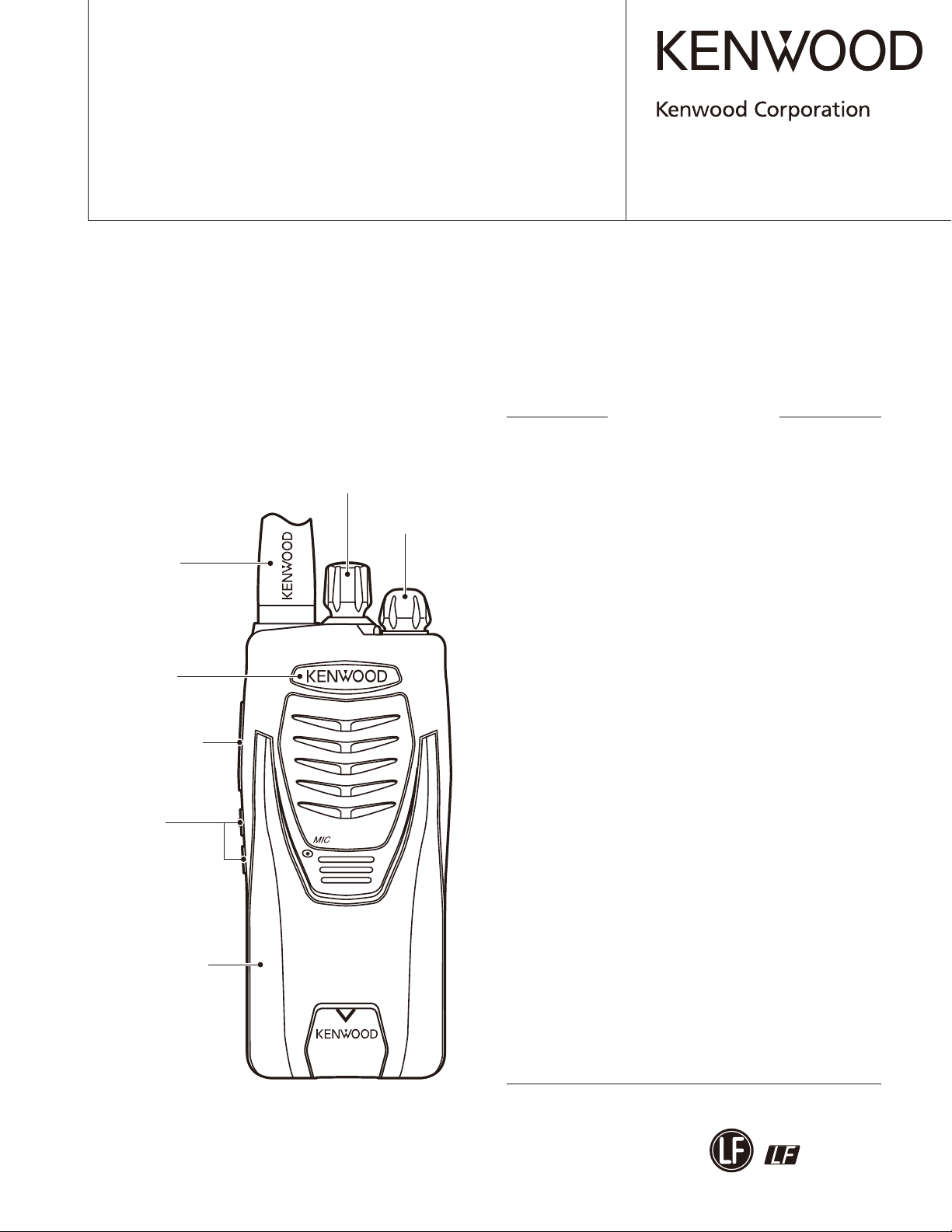
Whip antenna
(T90-1039-25)
Badge
(B43-1190-04)
Button knob (PTT)
(K29-9308-23)
Button knob
(Lock/Scan)
(K29-9364-03)
Knob (Channel)
(K29-9318-03)
Knob (Volume)
(K29-9309-03)
GENERAL .....................................................2
REALIGNMENT ...........................................3
DISASSEMBLY FOR REPAIR ......................5
CIRCUIT DESCRIPTION ..............................8
SEMICONDUCTOR DATA .........................11
COMPONENTS DESCRIPTION .................12
TERMINAL FUNCTION .............................12
PARTS LIST ...............................................13
EXPLODED VIEW ......................................19
PACKING ....................................................20
ADJUSTMENT ..........................................21
LEVEL DIAGRAM ......................................25
PC BOARD
TX-RX UNIT (X57-6900-21) ...................26
SCHEMATIC DIAGRAM ............................30
BLOCK DIAGRAM .....................................34
Plastic cabinet assy
(A02-4043-03)
OPTIONAL ACCESSORIES
KBH-10 (Belt Clip) ..................................36
KNB-30A (Ni-Cd Battery Pack) .............36
KSC-31 (Rapid Charger) ........................36
SPECIFICATIONS ......................................37
This product uses Lead Free solder.

TK-361SA
GENERAL
Document Copyrights
Copyright 2008 by Kenwood Corporation. All rights re-
served.
No part of this manual may be reproduced, translated,
distributed, or transmitted in any form or by any means,
electronic, mechanical, photocopying, recording, or otherwise, for any purpose without the prior written permission
of Kenwood.
Disclaimer
While every precaution has been taken in the preparation
of this manual, Kenwood assumes no responsibility for errors or omissions. Neither is any liability assumed for damages resulting from the use of the information contained
herein. Kenwood reserves the right to make changes to any
products herein at any time for improvement purposes.
INTRODUCTION
SCOPE OF THIS MANUAL
This manual is intended for use by experienced tech ni cians familiar with similar types of commercial grade com mu ni ca tions equipment. It contains all required service
in for ma tion for the equipment and is current as of the publication date. Changes which may occur after publication
are covered by either Service Bulletins or Manual Revisions.
These are is sued as required.
ORDERING REPLACEMENT PARTS
When ordering replacement parts or equipment in for ma tion, the full part identifi cation number should be in clud ed.
This applies to all parts : components, kits, or chassis. If the
part number is not known, include the chassis or kit number
of which it is a part, and a suffi cient description of the re quired component for proper identifi cation.
PERSONAL SAFETY
The following precautions are recommended for personal
safety:
• DO NOT transmit until all RF connectors are verifi ed se-
cure and any open connectors are properly terminated.
• SHUT OFF and DO NOT operate this equipment near
elec tri cal blasting caps or in an explosive atmosphere.
• This equipment should be serviced by a qualifi ed tech ni -
cian only.
SERVICE
This transceiver is designed for easy servicing. Refer
to the sche mat ic diagrams, printed circuit board views, and
align ment procedures contained within.
Destination Number Of CH Frequency No. / Frequency Factory default CH setting RF power output
CH1 463.975MHz / QT 94.8Hz
CH2 464.125MHz / QT 88.5Hz
CH3 464.175MHz / QT 103.5Hz
CH4 464.325MHz / QT 79.7Hz
CH5 464.375MHz / QT 107.2Hz
CH6 OFF
CH7 OFF
CH8 OFF
2W
M 8 channel
CH1 463.975MHz
CH2 464.125MHz
CH3 464.175MHz
CH4 464.325MHz
CH5 464.375MHz
2
1. Modes
User mode
PC mode
Clone mode
Self programming mode
REALIGNMENT
Data programming mode
PC test mode PC tuning mode
TK-361SA
Power switch/Volume control
t
Turn clockwise to switch the power ON and counter-
clockwise to switch the power OFF. Rotate to adjust the
volume.
LED indicator
y
Indicates the transceiver status. Lights red while trans-
mitting, green while receiving, and fl ashes red when the
battery power is low while transmitting.
Mode Function
User mode For normal use.
PC mode
Data programming
mode
PC test mode
Clone mode
Self programming
mode
Used for communication between the transceiver and PC.
Used to read and write frequency data and
other features to and from the transceiver.
Used to check the transceiver using the PC.
This feature is included in the KPG-88D(M2).
Used to transfer programming data from one
transceiver to another.
Used to program the transceiver without any
external programming device.
2. How to Enter Each Mode
Mode Operation
User mode Power ON
PC mode Received commands from PC
Clone mode [PTT]+[Side2]+Power ON (Two seconds)
Self programming
mode
[PTT]+[Side1]+Power ON (Two seconds)
3. Getting Acquainted
=
;
Antenna
B
:
@
.
Speaker/
microphone
jacks
Battery pack
(KNB-30A)
4. PC Mode
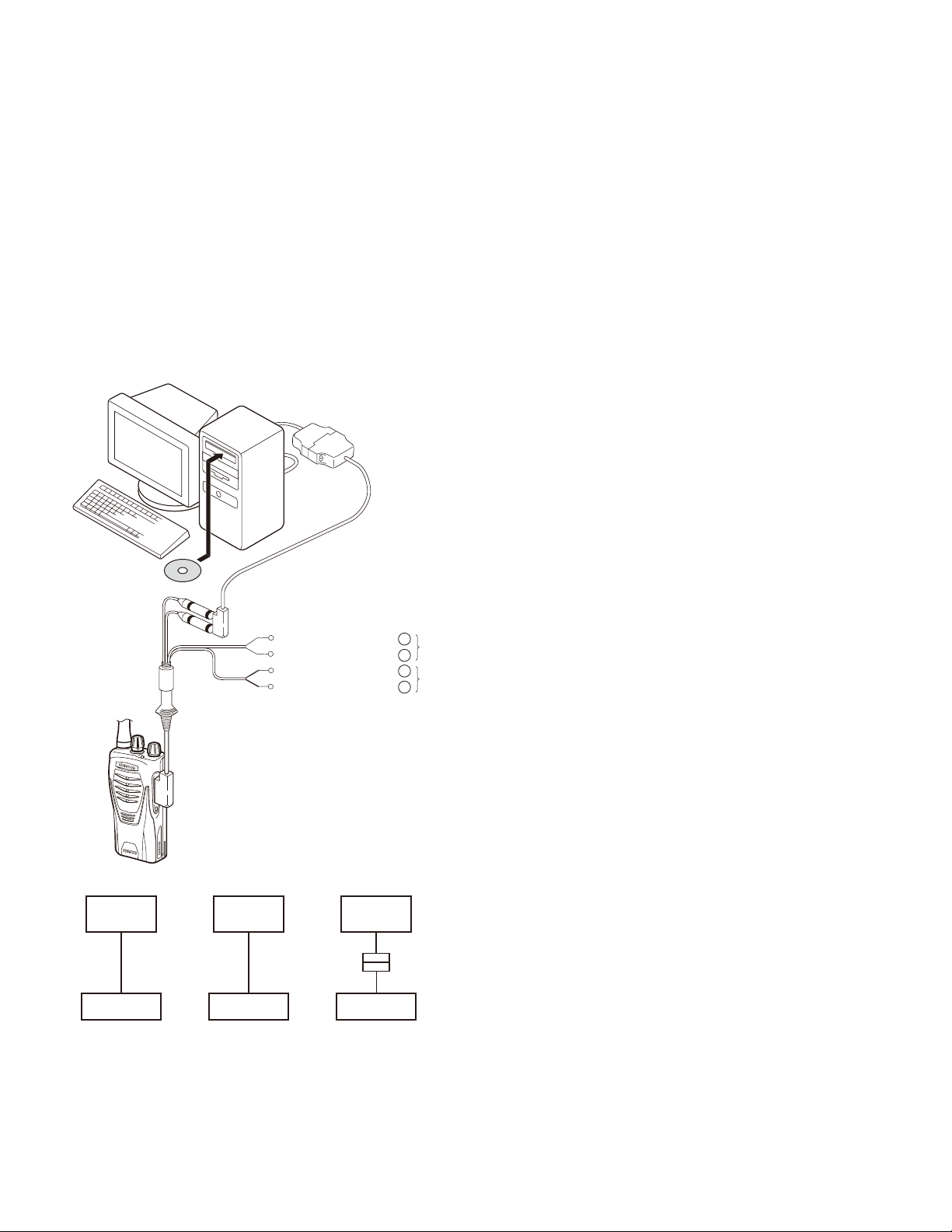
4-1. Preface
The transceiver is programmed by using a personal computer, a programming interface (KPG-22/22A, USB adapter
(KCT-53U)) and programming software (KPG-88D(M2)).
The programming software can be used with a PC. Figure 1 shows the setup of a PC for programming.
4-2. Connection Procedure
1. Connect the transceiver to the personal computer with
the interface cable and USB adapter (when the interface
cable is KPG-22A, the KCT-53U can be used.).
Notes:
• You must install the KCT-53U driver in the computer to
used the USB adapter (KCT-53U).
• When using the USB adapter (KCT-53U) for the fi rst time,
plug the KCT-53U into a USB port on the computer with
the computer power ON.
2. When the POWER is switched on, user mode can be en-
tered immediately. When the PC sends a command, the
transceiver enters PC mode.
When data is transmitting from the transceiver, the red
LED lights.
When data is received by the transceiver, the green LED
lights.
Notes :
• The data stored in the personal computer must match
Model Name when it is written into EEPROM.
• Change the transceiver to PC mode, then attach the in-
terface cable.
4-3. KPG-22/KPG-22A Description
(PC programming interface cable : Option)
The KPG-22/22A is required to interface the transceiver
with the computer. It has a circuit in its D-sub connector
(KPG-22: 25-pin, KPG-22A: 9-pin) case that converts the RS232C logic level to the TTL level.
The KPG-22/22A connects the SP/MIC connector of the
transceiver to the RS-232C serial port of the computer.
PTT (Push to Talk) switch
q
Press and hold, then speak into the microphone to trans-
mit.
Side 1 key
w
Super lock (default).
Side 2 key
e
Scan + Temporary delete (default)
Channel selector
r
Rotate to change the operating channel.
4-4. KCT-53U Description (USB adapter : Option)
The KCT-53U is a cable which connects the KPG-22A to
a USB port on a computer.
When using the KCT-53U, install the supplied CD-ROM
(with driver software) in the computer. The KCT-53U driver
runs under Windows 2000 or XP.
3
TK-361SA
REALIGNMENT
4-5. Programming Software Description
The KPG-88D(M2) is the programming software for the
transceiver supplied on a CD-ROM. The software on this
disk allows a user to program the transceiver radios via Programming interface cable (KPG-22/22A).
4-6. Programming with PC
If data is transferred to the transceiver from a PC with
the KPG-88D(M2), the data for each set can be modifi ed.
Data can be programmed into the EEPROM in RS-232C
format via the SP/MIC jack.
In this mode the PTT line operate as TXD and RXD data
lines respectively.
PC
KPG-88D(M2)
Tuning cable
(E30-3216-05)
KPG-22 or KPG-22A or
KPG-22A+KCT-53U
Illustration is KPG-22
Gray
Gray/Black
1.5D-XV Lead wire
1.5D-XV Shield wire
+
SP
–
+
MIC
–
5. Clone Mode
5-1. Outline
“Clone Mode” copies the transceiver data to another
transceiver.
The dealer can copy the transceiver data to another
transceiver even without the use of a personal computer.
5-2. Example
The transceiver can copy the programming data to one
or more transceivers via RF communication.
The clone source and clone target/s must be in Clone
mode.
5-3. Operation
1. To switch the clone target/s to Clone mode, press and
hold the [PTT] and [Side2] keys while turning the transceiver power ON.
2. Wait for 2 seconds. The LED will light orange and the
transceiver will announce “Clone”.
3. Select a channel table number using Lock (increment
channel table) and Scan(decrement channnel table) keys.
4. To switch the clone source to Clone mode, press and
hold the [PTT] and [Side2] keys while turning the transceiver power ON.
5. Wait for 2 seconds. The LED will light orange and the
transceiver will announce “Clone”.
6. Select the same channel table number as the clone target/s.
7. Press [PTT] on the clone source to begin data transmission.
When the clone target starts to receive data, the LED
will light green.
When the clone source fi nishes sending data, a “confi r-
mation” tone will sound.
If data transmission fails while cloning, an “error” tone
will sound from the target unit.
8. If the cloning fails, no data will be available in the target
unit when it is returned to User mode.
9. When the cloning is successful, the target unit’s “Scan”
function will return to their default values (Scan = OFF).
4
PC
D-SUB
(25-pin)
KPG-22
Transceiver
PC
D-SUB
(9-pin)
KPG-22A
Transceiver
Fig. 1
PC
USB
KCT-53U
KPG-22A
Transceiver
Notes:
• The dealer can clone data to two or more transceivers by
repeating the above procedures.
• If the transceivers Clone Mode is configured as “Disabled”, the transceiver cannot enter Clone mode.
• The table shown below will cover the frequency tables
used for wireless cloning.
• Clone mode cannot be entered in battery low state.
• A unit cannot be a “Source Unit” if it is unprogrammed.
If [PTT] is pressed, an “error” tone will sound.
• Once a unit is set to be the source, it cannot be a target
after the data has been transmitted. This protects the
data in the source unit.
• If the target unit is cloned successfully, it will return to
User Mode.
• If the target unit is not cloned successfully, the led will
remain Orange.
REALIGNMENT
TK-361SA
• The source Unit and target Unit must be of the same
model type and destination in order for Clone to operate.
• Clone mode cannot be accessed if “Super Lock” is activated.
• Electronic interface may cause a failure in data transfer
during Wireless Clone, such as when waveforms or electromagnetics are being performed at the workbench.
• Clone mode can be used ONLY by the authorized service
personnel.
• The Clone mode setting must be confi gured as “Disable”
before being delivered to the end-user.
• To clone, replace the antenna from both the source transceiver and the target transceiver with a dummy load.
• The transmit output power is automatically set to Low in
Clone mode.
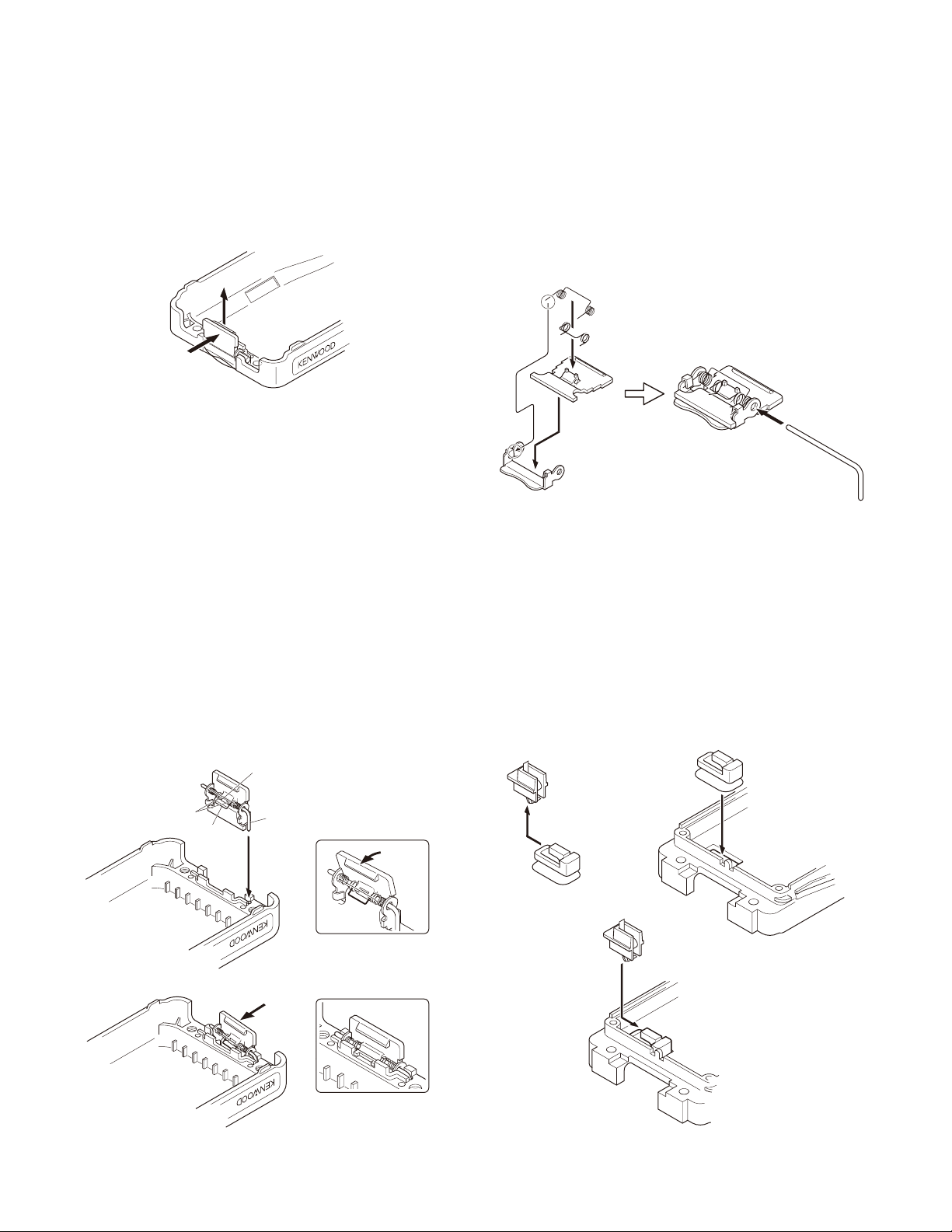
DISASSEMBLY FOR REPAIR
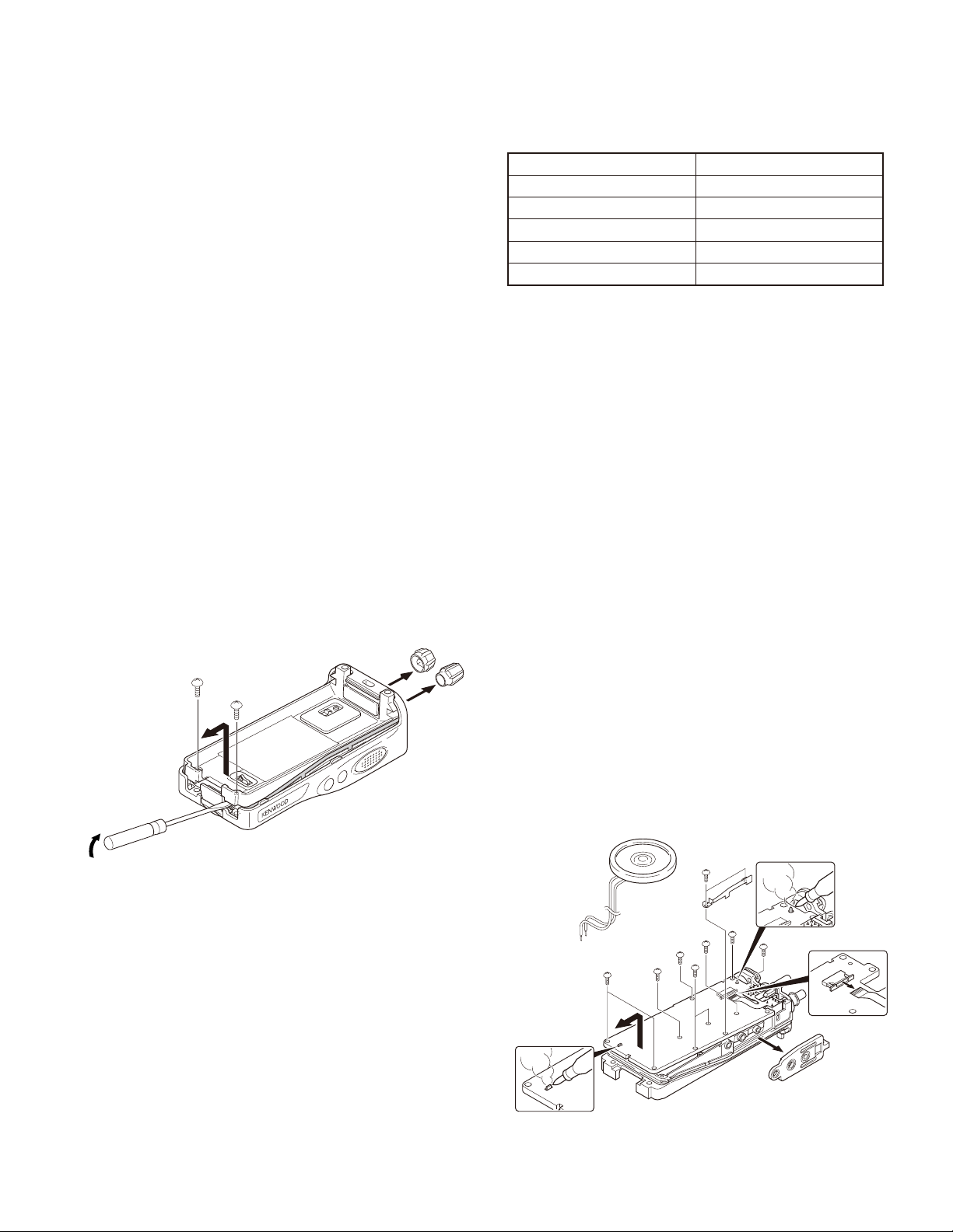
Removing the case assembly from the chassis
■
1. Remove the volume knob q and channel knob w.
2. Remove the two screws e.
3. Lift and remove the chassis from the case assembly r.
(Use a fl at-blade screwdriver to easily lift the chassis.)
:
@
.
.
;
Clone Frequency Table
Table number Frequency (MHz)
1 463.9750
2 464.1250
3 464.1750
4 464.3250
5 464.3750
Removing the TX-RX unit from the chassis
■
1. Remove the packing t from the SP/MIC jack of the TXRX unit.
2. Remove the eleven screws y fi xing the TX-RX unit.
3. Remove the fi xing bracket u of the SP/MIC.
4. Remove the solder of the antenna terminal with a soldering iron i.
5. Remove the solder of the positive terminal with a soldering iron o.
Note: You can remove the TX-RX unit from the chassis
without removing the solder at the positive terminal.
However, in this case, you can not attach the packing
(G53-1605-03) that is on the positive terminal to the
chassis in assembling. So, it is advisable to remove the
solder on the positive terminal fi rst.
6. Remove the FPC from the fl at cable connector !0.
7. Lift and remove the TX-RX unit from the chassis !1.
8
B
B
B
B
B
B
2
>
B
B
=
5
TK-361SA
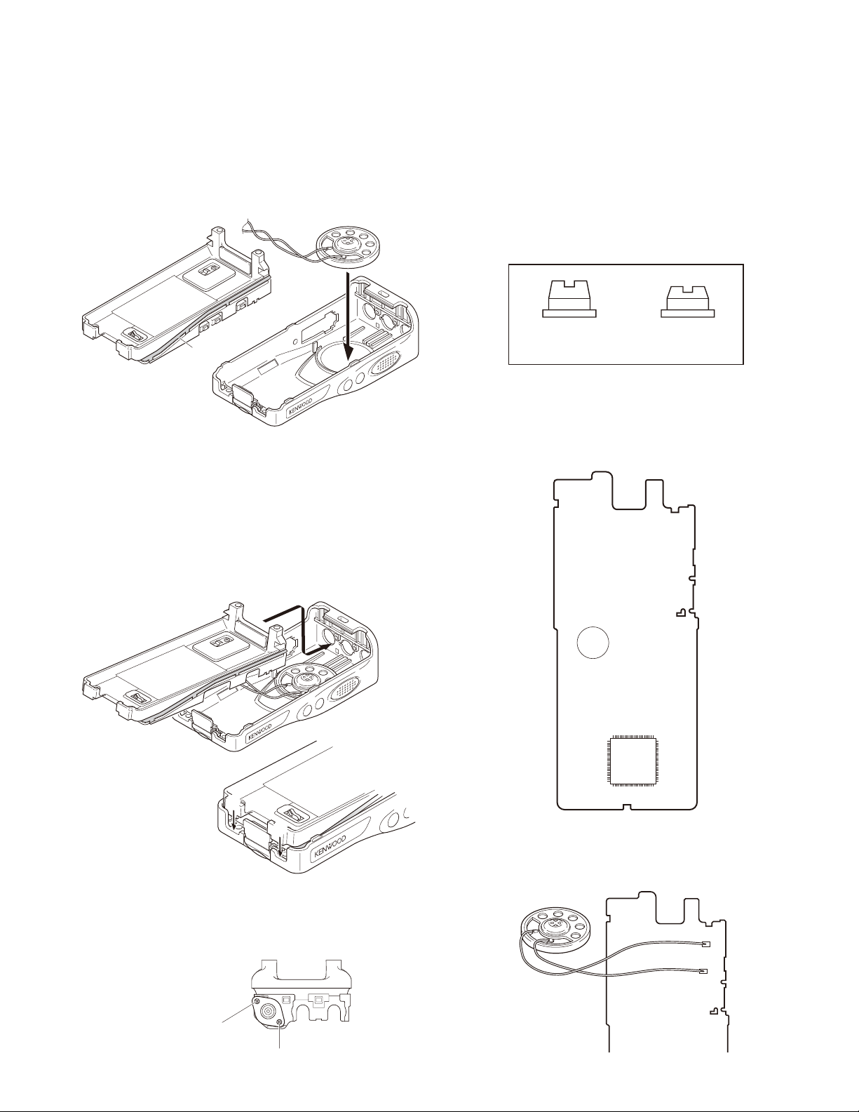
DISASSEMBLY FOR REPAIR
Removing the battery release lever from the
■
case assembly
1. Press the upper part of the lever toward the inside of the
case assembly. One side of the shaft will be removed q.
2. Lift and remove the battery release lever from the case
assembly w.
@
:
Attaching the battery release lever to the case
■
assembly
1. Insert one side of the shaft into the hole at the lever fi tting section on the case assembly q.
Caution: The thin spring (G01-4543-14) should be posi-
tioned above the two tabs of the lever.
2. Tilt the battery release lever slightly forward w, so that
the thick spring (G01-4542-04) is positioned below the
case surface.
3. With the thick spring positioned below the case surface,
attach the other side of the shaft to the case assembly
by pressing the battery release lever e until it snaps into
place r.
Caution: Be careful not to tilt the battery release lever
too forward.
If the battery release lever is pushed in this state where
the two tabs come below the case surface, there is a
possibility of damaging the two tabs.
Assembling the battery release lever
■
1. Place the lever w onto the stopper q.
2. Place the thick spring e onto the lever.
3. Hook the right and left ends of the thin spring r onto
the tabs of the stopper, then place the thin spring onto
the lever t.
4. Slide the shaft through the hole of the stopper and lever
.
y
;
.
=
:
Cautions for assembly
■
@
B
1. Attaching the positive terminal to the chassis
Always attach the positive terminal to the chassis, using
the following procedures, before mounting the TX-RX
unit onto the chassis.
1. Remove the holder assembly w from the packing q of
the positive terminal.
2. Mount the packing of the positive terminal into the chassis hole e.
3. Mount the holder assembly into the packing of the positive terminal r.
@
.
:
;
Two tabs
A thick spring
A thin spring
Shaft
@
:
.
;
6
DISASSEMBLY FOR REPAIR
TK-361SA
2. Mounting the chassis to the case assembly
1. Confirm that the waterproof packing attached to the
circumference of the chassis is securely inserted in the
groove of the chassis q.
2. Attach the speaker to the speaker recess of the case assembly w. Make sure the speaker is securely inserted.
@
:
Confirm that the
waterproof packing is
securely inserted in the
groove of the chassis.
3. Insert the upper part of the chassis into the case assembly e.
Caution: Take care that the speaker lead wire is not
caught by the microphone element.
4. Press the chassis r and the case assembly together to
attach them.
Caution: If the packing of the SP/MIC does not come
to the correct position after attaching the chassis to the
case assembly, reposition the packing with your fi ngers.
.
4. The nuts of the volume knob and channel knob
Note that the shapes, colors and heights of nuts of the
volume knob and channel knob are different from one
another. (The nut of volume knob is stainless steel, and
the nut of channel knob is brass)
Use the following jig when removing the nuts of the vol-
ume knob and channel knob.
• Jig (Part No. : W05-1012-00)
Volume Knob
(Stainless steel)
Channel Knob
(Brass)
5. Screw sequence for mounting the TX-RX unit to
the chassis
Attach the TX-RX unit to the chassis using the screws in
the order shown in the drawing below.
2
8
>
=
B
:
;
;
;
3. Attaching the antenna receptacle to the chassis
Screw the antenna receptacle to the chassis in the order
shown in the drawing so that the antenna receptacle
comes to the center of the case hole.
Tighten this screw first.
Tighten this screw second.
@
TX-RX UNIT
Component side view
.
6. Connecting the speaker wires to the TX-RX unit
Note: To connect the speaker wires, you must solder it
to the location of the TX-RX unit as illustrated below.
SP–
SP+
TX-RX UNIT
Component
side view
7
TK-361SA
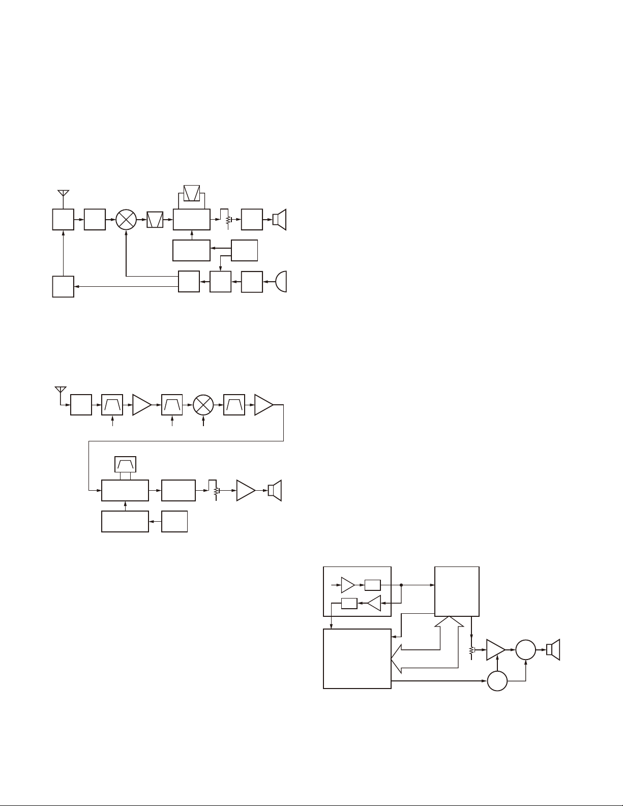
CIRCUIT DESCRIPTION
1. Frequency Confi guration
The receiver utilizes double conversion. The first IF is
38.85MHz and the second IF is 450kHz. The fi rst local oscillator signal is supplied from the PLL circuit.
The PLL circuit in the transmitter generates the neces-
sary frequencies. Fig. 1 shows the frequencies.
CF
ANT
463.975~464.375MHz
ANT
SW
TX
AMP
RF
AMP
425.125~
425.525MHz
463.975~464.375MHz
1st MIX
MCF
38.85MHz
450kHz
IF
SYSTEM
38.4MHz
X3
multiply
RF
AMP
PLL
VCO
AF
AMP
TCXO
MIC
AMP
SP
12.8MHz
MIC
Fig. 1 Frequency confi guration
2. Receiver
The frequency confi guration of the receiver is shown in
Fig. 2.
ANT
ANT
SW
Front End (RF AMP)
■
The signal coming from the antenna passes through the
transmit/receive switching diode circuit, (D103, D104,
D106 and D122) passes through a BPF (L229 and L228), and
is amplifi ed by the RF amplifi er (Q205).
The resulting signal passes through a BPF (L214, L212
and L211) and goes to the mixer (Q204). These BPFs are
adjusted by variable capacitors (D203, D204, D205, D206
and D210). The input voltage to the variable capacitor is regulated by voltage output from the micro control unit (MCU)
(IC405).
First Mixer
■
The signal from the front end is mixed with the fi rst local
oscillator signal generated in the PLL circuit by Q3 to produce a fi rst IF frequency of 38.85MHz.
RF AMP
BPF
Q205
PCTV
CF201
IC201
IF, MIX, DET
Q1
X3 multiply
2nd Local 12.8MHz
BPF
PCTV
IC301
AQUA-L
X1
TCXO
MIXER
Q204
1st Local
AF VOL
Fig. 2 Receiver section
MCF
XF201
IC302
AF PA
IF AMP
Q203
SP
The resulting signal passes through the XF201 MCF to
cut the adjacent spurious and provide the opitimun characteristics, such as adjacent frequency selectivity.
IF Amplifi er Circuit
■
The fi rst IF signal is passed through a four-pole monolithic crystal fi lter (XF201) to remove the adjacent channel
signal.
The fi ltered fi rst IF signal is amplifi ed by the fi rst IF amplifi er (Q203) and then applied to the lF system IC (IC201). The
IF system IC provides a second mixer, second local oscillator, limiting amplifi er, quadrature detector and RSSI (Received
Signal Strength Indicator). The second mixer mixes the fi rst
IF signal with the 38.4MHz of the second local oscillator
output (Q1) and produces the second IF signal of 450kHz.
The second IF signal is passed through the ceramic fi lter
(CF201) to remove the adjacent channel signal. The fi ltered
second IF signal is amplified by the limiting amplifier and
demodulated by the quadrature detector with the ceramic
discriminator (CD201). The demodulated signal is routed to
the audio circuit.
Audio Amplifi er Circuit
■
The demodulated signal from IC201 goes to AF amplifi er
through IC301.
The signal then goes through an AF volume control, and
is routed to an audio power amplifi er (IC302) where it is amplifi ed and output to the speaker.
Squelch
■
Part of the AF signal from the IC enters the FM IC (IC201)
again, and the noise component is amplifi ed and rectifi ed by
a fi lter and an amplifi er to produce a DC voltage corresponding to the noise level.
The DC signal from the FM IC goes to the analog port
of the MCU (IC405). IC405 determines whether to output
sounds from the speaker by checking whether the input
voltage is higher or lower than the preset value.
To output sounds from the speaker, IC405 sends a high
signal to the SP MUTE line and turns IC302 on through
Q303, Q304, Q305, Q306 and Q316. (See Fig. 3)
IC201 FM IF
IF AMP
BUSY
QT/DQT IN
IC405
MCU
AF CONT
SIGNAL
QT/DQT
CLK, DATA,
STD, LOADN
IC301
AQUA-L
Q306,316
IC302
AF PA
Q303,304,305
SW
SW
SP
Fig. 3 AF amplifi er and squelch
8
CIRCUIT DESCRIPTION
TK-361SA
Receive Signaling
■
• QT/DQT
The output signal from FM IC (IC201) enters the MCU
(IC405) through IC301. IC405 determines whether the QT or
DQT matches the preset value, and controls the SP MUTE
and the speaker output sounds according to the squelch results.
3. PLL Frequency Synthesizer
The PLL circuit generates the fi rst local oscillator signal
for reception and the RF signal for transmission.
PLL
■
The frequency step of the PLL circuit is 5 or 6.25kHz.
A 12.8MHz reference an oscillator signal is divided at IC1
by a fi xed counter to produce oscillator (VCO) output signal
which is buffer amplifi ed by Q2 then divided in IC1 by a programmable counter. The divided signal is compared in phase
with the 5 or 6.25kHz reference signal from the phase comparator in IC1. The output signal from the phase comparator
is fi ltered through a low-pass fi lter and passed to the VCO
to control the oscillator frequency. (See Fig. 4)
VCO
■
The operating frequency is generated by Q4 in transmit
mode and Q3 in receive mode. The oscillator frequency is
controlled by applying the VCO control voltage, obtained
from the phase comparator, to the varactor diodes (D2, D4,
D6 and D7 in transmit mode and D3, D5, D8 and D9 in receive mode). The RX pin is set high in receive mode causing
Q5 turn on.
The TX pin is set high in transmit mode. The outputs
from Q3 and Q4 are amplifi ed by Q6 and sent to the RF amplifi ers.
LPF
LPF
D2,4
D6,7
D3,5
D8,9
Q4
TX VCO
Q3
RX VCO
Q6
BUFF AMP
Q5,7
T/R SW
Q2
RF AMP
Q9
RF AMP
RX
TX
Unlock Detector
■
If a pulse signal appears at the LD pin of IC1, an unlock
condition occurs, and the DC voltage obtained from C4, R5,
and D1 causes the voltage applied to the MCU (IC405) to go
low. When the MCU detects this condition, the transmitter
is disabled, ignoring the push-to-talk switch input signal.
4. Transmitter System
Microphone Amplifi er
■
The signal from the microphone passes through IC301.
The signal passes through the Audio processor (IC301)
for the maximum deviation adjustment, and goes to the
VCO modulation input.
MIC
AGC
IC405
MCU
AQUA-L
LPF
BEEP
IC301
QTVCO
QTTCXO
LPF
LPF TCXO
Fig. 5 Microphone amplifi er
Drive and Final Amplifi er
■
The signal from the T/R switch (D101) is amplifi ed by the
pre-drive (Q101) to 50mW.
The output of the drive amplifi er is amplifi ed by the RF
power amplifier (Q102 and Q103) to 2W (1W when the
power is low). The RF power amplifi er consists of two MOS
FET stages. The output of the RF power amplifi er is then
passed through the harmonic fi lter (LPF) and antenna switch
(D103 and D122) and applied to the antenna terminal.
Q101 Q102
Pre-drive
AMP
VD
5T5T
R127
R128
R129
Drive
AMP
VGVG
Q103
Final
AMP
VG
VDD
T/R SW
(D101)
Q100
RF
AMP
+B
VCO
D103,122
ANT
SW
X1
ANT
LPF
PLL DATA
X1
12.8MHz
5kHz/6.25kHz
1/N
REF OSC
1/M
5kHz/6.25kHz
Fig. 4 PLL circuit
Phase
comparator
Charge
pump
IC1
PLL IC
PCTV
(IC405)
IC101
(1/2)
IC101
(2/2)
Fig. 6 Drive and fi nal amplifi er and APC circuit
APC Circuit
■
The APC circuit always monitors the current flowing through the RF power amplifi er (Q102 and Q103) and
keeps a constant current. The voltage drop at R127, R128
and R129 is caused by the current fl owing through the RF
power amplifi er and this voltage is applied to the differential
amplifi er IC101 (1/2).
9
TK-361SA
CIRCUIT DESCRIPTION
IC101 (2/2) compares the output voltage of IC101 (1/2)
with the reference voltage from MCU (IC405). The output of
IC101 (2/2) controls the VG of the RF power amplifi er, Drive
amplifi er and Pre-Drive amplifi er to make both voltages the
same.
The change of power high/low is carried out by the
change of the reference voltage.
Encode Signaling
■
• QT/DQT
QT,DQT data of the QTTCXO Line is output from pin 28
of the MCU (IC405). The signal passes through a low-pass
CR fi lter and goes to the TCXO (X1).
The QT,DQT data of the QTVCO Line is output from pin
24 of the MCU. The signal passes through a low pass CR fi lter, mixes with the audio signal, and goes to the VCO modulation input. TX deviation is adjusted by the MCU.
5. Power Supply
There are four 5V power supplies 5M, 5C, 5R, and 5T.
5M for MCU (IC405) is always output while the power is on.
5M is always output, but turns off when the power is
turned off to prevent malfunction of the MCU.
5C is a common 5V and is output when SAVE is not set
to OFF.
5R is 5V for reception and output during reception.
5T is 5V for transmission and output during transmission.
Memory Circuit
■
Memory circuit consists of the MCU (IC405) and an EEPROM (IC406). An EEPROM has a capacity of 64k bits that
contains the transceiver control program for the MCU and
data such as transceiver channels and operating features.
IC405
MCU
IC406
EEPROM
Fig. 8 Memory circuit
Low Battery Warning
■
The battery voltage is checked by the MCU (IC405).
The transceiver generates a warning tone when it falls
below the warning voltage shown in the table.
(1) The red LED blinks when the battery voltage falls below
the voltage (1) shown in the table during transmission.
Note:
The transceiver checks the battery voltage during recep-
tion even when, in the FPU, the Battery Warning status
function is set to “On TX” (default setting).
However, the LED does not blink during reception. Dur-
ing transmission, the LED blinks to generate the warning
tone of a low battery voltage.
(2) The transceiver immediately stops transmission when
the battery voltage falls below the voltage (2) shown in
the table. A message tone beeps while the PTT switch is
released.
6. Control Circuit
The control circuit consists of a MCU (IC405) and its
peripheral circuits. It controls the TX-RX unit. IC405 mainly
performs the following:
(1) Switching between transmission and reception by the
PTT signal input.
(2) Reading system, group, frequency, and program data
from the memory circuit.
(3) Sending frequency program data to the PLL.
(4) Controlling squelch on/off by the DC voltage from the
squelch circuit.
(5) Controlling the audio mute circuit by the decode data in-
put.
(6) Transmitting tone and encode data.
Frequency Shift Circuit
■
The MCU (IC405) operates at a clock of 7.3728MHz. This
oscillator has a circuit that shifts the frequency by BEAT
SHIFT SW (Q407, Q408).
A beat sound may be able to be evaded from generation
if “Beat Shift” is set to ON when it is generated in the internal spurious transmission modulated sound of a transceiver.
IC405
MCU
BSHIFT
XIN
XOUT
X2
Q408
H: OFF
L: ON
Q407
H: OFF
L: ON
Ni-Cd Battery
(1) 6.2V
(2) 5.9V
R404
SB
88
R406
BATT
IC405
MCU
Fig. 9 Low battery warning
7. Control System
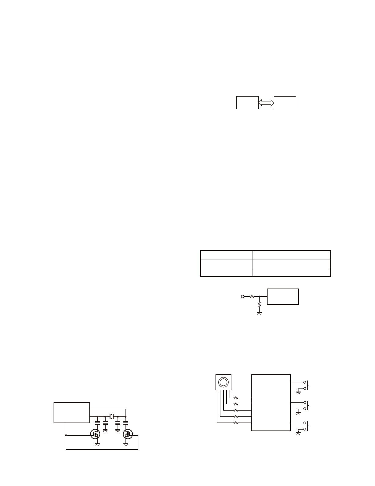
Keys and channel selector circuit.
The signal from keys and channel selector input to MCU
(IC405) directly as shown in fi g. 10.
Channel selector
IC405
MCU
50
EN1
49
EN2
48
EN3
47
EN4
46
EN5
Fig. 10 Control system
PTT
PF1
PF2
27
PTT SW
74
SW1
75
SW2
10
Fig. 7 Frequency shift circuit

SEMICONDUCTOR DATA
Micro Control Unit: 30622MAP490GU (TX-RX unit IC405)
Pin No.
1 PCTV O APC/BPF control data output
2 BEEP O BEEP Output
3NC -NC
4 EEPDAT I/O EEPROM data input/output
5 EEPCLK O EEPROM clock output
6 BYTE - GND
7 GND - GND
8 BSHIFT O Beat shift switch
9NC -NC
10 RESET I CPU reset
11 XOUT O CPU clock (7.3728MHz)
12 VSS - GND
13 XIN I CPU clock (7.3728MHz)
14,15 VCC - +5V
16 INT I Battery voltage monitor input
17 TCLK/DTRDO I Base band IC data input
18 RDF/FD I Base band IC data input
19 SCLK O Base band IC clock output
20 D I/O I/O Base band IC data input/output
21
22 DIR O Base band IC data output
23 STD I Base band IC data input
24 QT VCO O QT/DQT output
25 DTRLOADN O Base band IC data output
26 1/2 OSC O 3.6864MHz (7.3728MHz/2)
27 PTT I PTT switch input
28 QT TCXO O QT/DQT output
29 TXD O Serial data (FPU/FLASH)
30 RXD I Serial data (FPU/FLASH)
31 GND - GND
32 APCSW O APC switch
33,34 NC - NC
35 DCSW O APC voltage discharge switch
36 - - Not used
37 RX_SW O RX VCO switch
38 TX_SW O TX VCO switch
39 GND - GND
40 PLL_UL I PLL unlock detect input
41 PLL_STB O PLL strobe output
42 PLL_DAT O PLL data output
43 PLL_CLK O PLL clock output
Pin Name I/O Function
TDATA/DTRCLK
O Base band IC data output
Pin No.
44 VCC - +5V
45 - - Not used
46 EN5 I Channel selectable input
47 EN4 I Channel selectable input
48 EN3 I Channel selectable input
49 EN2 I Channel selectable input
50 EN1 I Channel selectable input
51 OPTDET I Headset input detect
52 AF_CONT O Speaker mute
53
54 - - Not used
55~59
60 VCC - +5V
61 NC - NC
62 VSS - GND
63,64 GND - GND
65~71
72 LEDTX O Red LED lights control output
73 LEDRX O Green LED lights control output
74 PF1 I Lock key input
75 PF2 I Scan key input
76 SIM1 - GND
77 SIM2 - GND
78,79 NC - NC
80 5T_C O 5T control output
81 5R_C O 5R control output
82 5C_C O 5C control output
83~87
88 BATT I Battery voltage input
89 RSSI I
90 BUSY I Busy level input
91 VOX I VOX level input
92 QT/DQT_IN I QT/DQT input
93 TH_DET I Thermistor input
94 AVSS - GND
95 NC - NC
96 VREF - +5V
97 AVCC - +5V
98 NC - NC
99 MIC_Mute O MIC mute
100 NC - NC
Pin Name I/O Function
Calling Alert SW
NC - NC
NC - NC
NC - NC
TK-361SA
O Calling alert switch
Received Signal Strength Indicator input
11

TK-361SA
COMPONENTS DESCRIPTION
TX-RX Unit (X57-6900-21)
Ref. No. Part Name Description
IC1 IC PLL system
IC101 IC Comparator (APC)
IC201 IC FM IF system
IC301 IC Audio processor
IC302 IC AF AMP
IC401,402
IC403 IC Voltage detector/ Reset
IC404 IC Voltage detector/ Int
IC405 IC Micro control unit
IC406 IC EEPROM
Q1 Transistor Tripler
Q2 Transistor PLL IC f_in AMP
Q3 FET VCO/ RX
Q4 FET VCO/ TX
Q5 Transistor DC switch/ TX VCO
Q6 Transistor RF Buffer AMP
Q7 Transistor DC switch/ RX VCO
Q8 Transistor Ripple fi lter
Q9,100 Transistor RF AMP
Q101 FET Pre-drive AMP
Q102 FET TX Drive AMP
Q103 FET TX Final AMP
Q104 Transistor APC switch
Q105 FET APC switch
Q107 Transistor APC switch
Q108 FET APC switch
Q109 Transistor APC switch
Q203 Transistor IF AMP
Q204 FET Mixer
Q205 FET RF AMP
Q301 Transistor TX DEV adjustment
Q302 Transistor MIC AGC
Q303 Transistor DC switch/ SP Mute
Q304 Transistor DC switch
IC Voltage Regulator/ 5V
Ref. No. Part Name Description
Q305 Transistor DC switch/ SP Mute
Q306 FET SP Mute switch
Q316 FET SP Mute switch
Q317,318
Q401 Transistor LED switch/ Red
Q402 Transistor LED switch/ Green
Q403 FET 5T switch
Q404 FET 5R switch
Q405 Transistor 5C switch
Q407,408
D1 Diode Rectifi cation
D2
D3
D4
D5
D6,7
D8,9
D10
D11 Diode Current steering
D101 Diode TX/RX RF switch
D102 Zener Diode APC protect
D103,104
D106 Diode ANT switch
D122 Diode ANT switch
D202 Diode TX/RX RF switch
D203~206
D210
D301,302
D303 Diode Isolation
D401 Diode Reverse current protection
D402 Diode Reverse Protection
D403 LED LED/ Red
D404 LED LED/ Green
D405 Zener Diode Limiter
FET Audio switch
FET Beat Shift switch
Variable Capacitance Diode
Variable Capacitance Diode
Variable Capacitance Diode
Variable Capacitance Diode
Variable Capacitance Diode
Variable Capacitance Diode
Variable Capacitance Diode
Diode ANT switch
Variable Capacitance Diode
Variable Capacitance Diode
Diode Detector
Frequency control/ TX VCO
Frequency control/ RX VCO
Frequency control/ TX VCO
Frequency control/ RX VCO
Frequency control/ TX VCO
Frequency control/ RX VCO
Modulator
RF BPF tuning
RF BPF tuning
CN401
Pin No. Name I/O Function
1 B I B (Battery Voltage)
2 SB O Switched B
3 SP1 I Audio input
4 SP2 O Audio output
5 GND - GND
12
TERMINAL FUNCTION
Pin No. Name I/O Function
6 EN1 I Channel selector pulse input
7 EN2 I Channel selector pulse input
8 GND - GND
9 EN3 I Channel selector pulse input
10 EN4 I Channel selector pulse input
11 EN5 I Channel selector pulse input

PARTS LIST
TK-361SA
New Parts.
✽
Parts without Parts No. are not supplied.
Les articles non mentionnes dans le Parts No. ne sont pas fournis.
Teile ohne Parts No. werden nicht geliefert.
Ref. No.
indicates safety critical components.
New
Ad dress
Parts No. Description
parts
TK-361SA
1 1A A02-3944-13 PLASTIC CABINET (CABINET ASSY)
2 1A ✽ A02-4043-03 PLASTIC CABINET ASSY (8CH)
3 3A A10-4094-43 CHASSIS
4 1B A21-1645-23 DRESSING PANEL (CABINET ASSY)
6 1C B09-0680-03 CAP (SP/MIC) ACCESSORY
7 2B B11-1817-04 ILLUMINATION GUIDE
8 1B B43-1190-04 BADGE (CABINET ASSY)
9 1C ✽ B62-2096-00 INSTRUCTION MANUAL
11 1A D10-0649-03 LEVER (CABINET ASSY)
12 1A D21-0863-04 SHAFT (CABINET ASSY)
13 1A D32-0441-13 STOPPER (CABINET ASSY)
15 2A E04-0465-05 RF COAXIAL RECEPTACLE (SMA)
16 3B E23-1253-04 TERMINA L(BATT-)
17 2B E37-1175-05 PROCESSED LEAD WIRE (SP+)
18 2B E37-1176-05 PROCESSED LEAD WIRE (SP-)
20 3A F20-3353-14 INSULATING SHEET (CHASSIS BATT+)
22 2A G01-4542-04 COIL SPRING (CABINET ASSY)
23 1A G01-4543-14 COIL SPRING (CABINET ASSY)
24 2B G10-1330-04 FIBROUS SHEET (AUDIO IC)
25 2A G11-4283-04 RUBBER SHEET (FINAL FET)
26 2A G11-4313-04 SHEET (MIC ELEMENT)
27 3A G13-2033-04 CUSHION (BATT-)
28 3B G13-2034-14 CUSHION (BATT-)
29 3A G13-2038-24 CUSHION (CHASSIS-CERAMIC FILTER)
30 2A G13-2039-14 CUSHION (PCB-CERAMIC FILTER)
31 3B G13-2045-04 CUSHION (CHASSIS)
32 2B G13-2076-04 CUSHION (SPEAKER)
33 2B G13-2088-04 CUSHION (CHASSIS,VR,CH)
34 3A G53-1604-03 PACKING (CHASSIS)
35 3A G53-1605-03 PACKING (BATT+)
36 2B G53-1606-13 PACKING (VOL/CH/LED)
37 1B G53-1607-03 PACKING (SP/MIC)
38 2B G53-1608-03 PACKING (SPEAKER)
39 2A G53-1609-14 PACKING (MIC ELEMENT)
40 2B G53-1610-04 PACKING (SMA)
42 2C H12-3179-05 PACKING FIXTURE
43 3D ✽ H52-2246-02 ITEM CARTON CASE
45 1C J19-5472-03 HOLDER (SP/MIC) ACCESSORY
46 2A J19-5473-03 HOLDER ASSY (BATT+)
47 2B J21-8478-04 MOUNTING HARDWARE
48 2B J21-8525-03 MOUNTING HARDWARE
49 2C J29-0734-05 BELT HOOK ACCESSORY
50 2B J82-0092-05 FPC
Destination
L : Scandinavia K : USA P : Canada
Y : PX (Far East, Hawaii) T : England E : Eu rope
Y : AAFES (Europe) X : Australia M : Oth er Areas
TK-361SA (Y50-5920-21)
TX-RX UNIT (X57-6900-21)
Ref. No.
E 2A,2B N83-2005-48 PAN HEAD TAPTITE SCREW (PCB)
57 1C N99-2046-05 SCREW SET ACCESSORY
59 2B R31-0661-05 VARIABLE RESISTOR
61 2B S60-0435-05 ROTARY SWITCH
63 1B T07-0760-25 SPEAKER
64 1C T90-1039-25 WHIP ANTENNA ACCESSORY
66 2D ✽ W08-0969-35 CHARGER ACCESSORY
67 1D W08-0971-35 AC ADAPTER ACCESSORY
68 2D ✽ W09-1001-15 BATTERY ASSY ACCESSORY
Ad dress
New
Parts No. Description
parts
TX-RX UNIT (X57-6900-21)
D403 B30-2156-05 LED (RED)
D404 B30-2157-05 LED (YELLOW)
C1 CK73HB1H332K CHIP C 3300PF K
C2 CK73HB1C682K CHIP C 6800PF K
C3 CK73GB1A105K CHIP C 1.0UF K
C4 CK73HB1C103K CHIP C 0.010UF K
C5 CK73HB1H102K CHIP C 1000PF K
C6 CK73HB1A104K CHIP C 0.10UF K
C7,8 CC73HCH1H101J CHIP C 100PF J
C9 CC73HCH1H100C CHIP C 10PF C
C10 CS77CP0J100M CHIP TNTL 10UF 6.3WV
C11 CC73HCH1H101J CHIP C 100PF J
C12 CK73HB1H102K CHIP C 1000PF K
C13 CK73HB1A104K CHIP C 0.10UF K
C14 CK73HB1C103K CHIP C 0.010UF K
C15 CC73HCH1H100C CHIP C 10PF C
C16 CK73HB1H102K CHIP C 1000PF K
C17 CC73HCH1H470J CHIP C 47PF J
C18 CC73HCH1H180J CHIP C 18PF J
C19 CK73HB1A104K CHIP C 0.10UF K
C21 CS77CP0J100M CHIP TNTL 10UF 6.3WV
C22 CS77AA1VR33M CHIP TNTL 0.33UF 35WV
C24 CK73HB1H102K CHIP C 1000PF K
C25 CC73HCH1H020B CHIP C 2.0PF B
C26 CC73HCH1H300J CHIP C 30PF J
C27 CS77CA1C3R3M CHIP TNTL 3.3UF 16WV
C29,30 CK73HB1H471K CHIP C 470PF K
C32 CS77CA1V0R1M CHIP TNTL 0.1UF 35WV
C33,34 CK73HB1H102K CHIP C 1000PF K
C35 CC73HCH1H270J CHIP C 27PF J
C38 CC73HCH1H050B CHIP C 5.0PF B
C39 CK73GB1H332K CHIP C 3300PF K
Destination
52 1A K29-9308-23 BUTTON KNOB (CABINET ASSY)
53 1B K29-9309-03 KNOB (VOLUME)
54 1B K29-9318-03 KNOB (CHANNEL)
55 1A K29-9364-03 BUTTON KNOB (CABINET ASSY)
A 2B N14-0819-04 CIRCULAR NUT (VOLUME)
B 2B N14-0832-04 CIRCULAR NUT (CHANNEL)
C 2A,2B N30-2604-48 PAN HEAD MACHINE SCREW (SMA)
D 3A N30-2606-48
PAN HEAD MACHINE SCREW (CHASSIS)
C40 CC73HCH1H030B CHIP C 3.0PF B
C41 CK73GB1H682K CHIP C 6800PF K
C42 CC73HCH1H050B CHIP C 5.0PF B
C43 CC73HCH1H100C CHIP C 10PF C
C44 CK73HB1H471K CHIP C 470PF K
C45 CK73GB1A105K CHIP C 1.0UF K
C47 CC73HCH1H101J CHIP C 100PF J
C48 CK73HB1H471K CHIP C 470PF K
13
 Loading...