Kenwood TМ-271E Service Manual
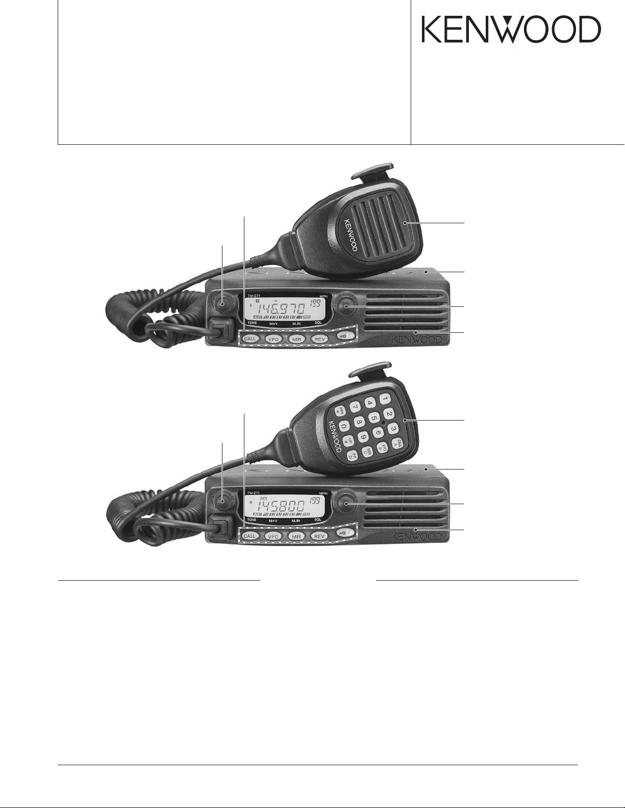
VHF FM TRANSCEIVER
TM-271A/271E
SERVICE MANUAL
TM-271A (M2,M4)
Key top
(K29-9291-01)
Knob (Volume)
(K29-9292-03)
© 2003-10 PRINTED IN JAPAN
B51-8663-00 (N) 743
Microphone
(T91-0624-05)
Cabinet
(A01-2193-01)
Knob (Encoder)
(K29-9293-03)
Panel assy
(A62-1088-03)
TM-271A/E (K,M3,E)
Key top
(K29-9291-01)
Knob (Volume)
(K29-9292-03)
CONTENTS
CIRCUIT DESCRIPTION ............................ 2
SEMICONDUCTOR DATA ........................ 8
COMPONENTS DESCRIPTION ................ 9
PARTS LIST ............................................. 10
Microphone
(T91-0641-05)
Cabinet
(A01-2193-01)
Knob (Encoder)
(K29-9293-03)
Panel assy
(A62-1088-03)
TERMINAL FUNCTION ........................... 27
PC BOARD
DISPLAY UNIT (X54-3450-10) ............ 28
TX-RX UNIT (X57-685X-XX)............... 30
EXPLODED VIEW.................................... 17
PACKING ................................................. 18
RESETTING THE TRANSCEIVER ........... 19
ADJUSTMENT ........................................ 20
SCHEMATIC DIAGRAM.......................... 34
BLOCK DIAGRAM ................................... 38
LEVEL DIAGRAM .................................... 40
SPECIFICATION ................... BACK COVER
TM-271A/271E
CIRCUIT DESCRIPTION
Frequency Configuration
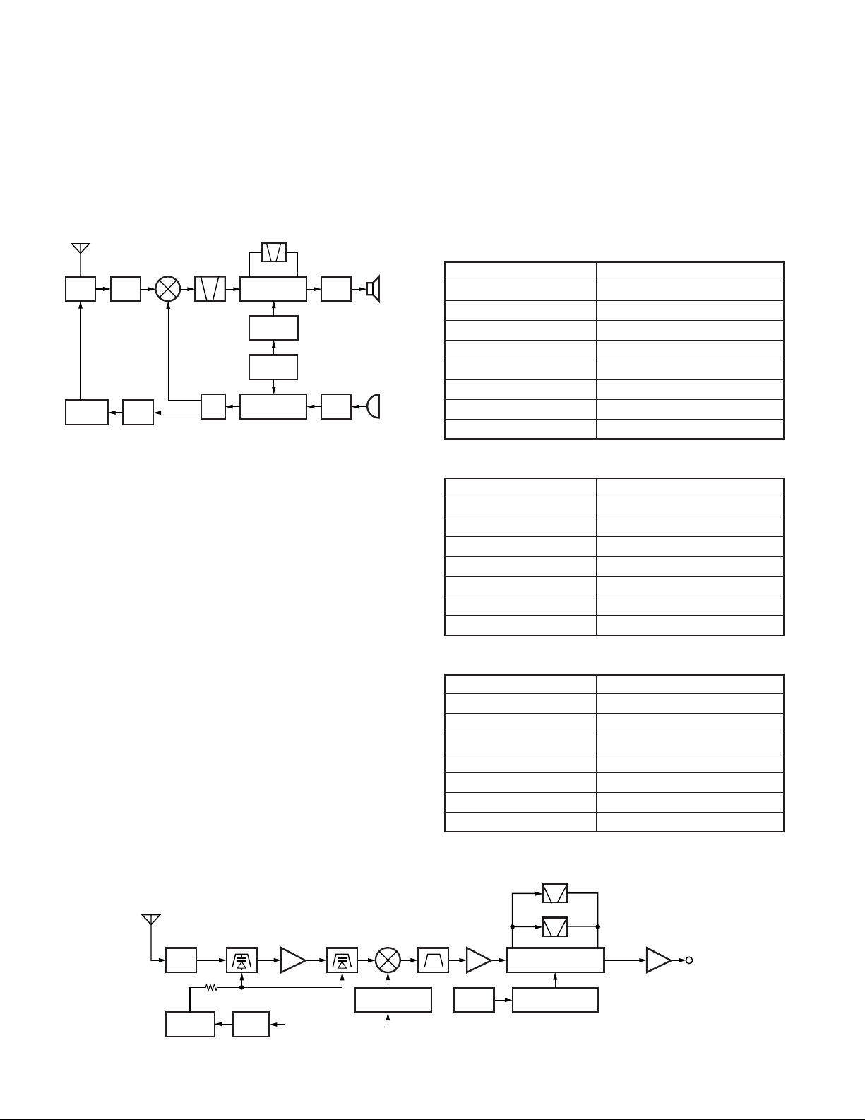
The receiver utilizes double conversion. The first IF is
49.95MHz and the second IF is 450kHz. The first local oscillator signal is supplied from the PLL circuit.
The PLL circuit in the transmitter generates the necessary
frequencies. Figure 1 shows the frequencies.
1/2
CF 450kHz
IF SYSTEM
50.4MHz
X3
multiply
TCXO
PLL/VCO
AF
PA
16.8MHz
MIC
AMP
SP
MIC
ANT
ANT
SWRFAMP
POWER
AMP
RF
AMP
1st
MIX
MCF
49.95MHz
RX
TX
Fig. 1 Frequency configuration
Receiver System
The receiver is double conversion superheterodyne. The
frequency configuration is shown in Figure 1.
■ Front-end RF Amplifier
An incoming signal from the antenna is applied to an RF
amplifier (Q353) after passing through a transmit/receive
switch circuit (D603, D605 are off) and a band pass filter
(L357, L356 and varactor diodes : D353, D354). After the
signal is amplified (Q353), the signal is filtered through a band
pass filter (L354, L355 and varactor diodes: D351, D352) to
eliminate unwanted signals before it is passed to the first
mixer.
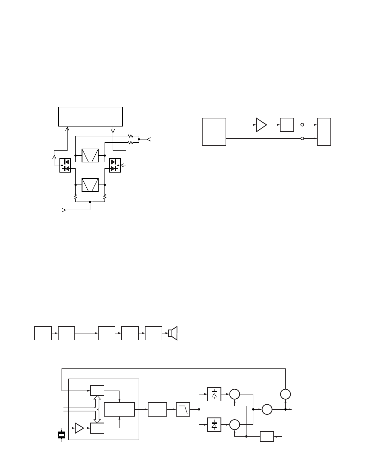
The voltage of these diodes are controlled by tracking the
CPU (IC101) center frequency of the band pass filter. (See
Fig. 2.)
■ First Mixer
The signal from the RF amplifier is heterodyned with the
first local oscillator signal from the PLL frequency synthesizer
circuit at the first mixer (Q352) to create a 49.95MHz first
intermediate frequency (1st IF) signal. The first IF signal is
then fed through one pair of monolithic crystal filter (MCF :
XF351) to further remove spurious signals.
■ IF Amplifier
The first IF signal is amplified by Q351, and then goes to
IC301 (FM processing IC). The signal is heterodyned again
with a second local oscillator signal within IC301 to create a
450kHz second IF signal. The second IF signal is then fed
through a 450kHz ceramic filter (Wide : CF301, Narrow :
CF302) to further eliminate unwanted signals before it is amplified and FM detected in IC301.
Item Rating
Nominal center frequency 49.95MHz
Pass bandwidth ±5.0kHz or more at 3dB
35dB stop bandwidth ±20.0kHz or less
Ripple 1.0dB or less
Insertion loss 5.0dB or less
Guaranteed attenuation 80dB or more at fo±1MHz
Spurious 40dB or more
Terminal impedance 350Ω / 5.5pF
Table 1 Crystal filter (L71-0620-05) : XF351
Item Rating
Nominal center frequency 450kHz
6dB bandwidth ±6.0kHz or more
50dB bandwidth ±12.5kHz or less
Ripple 2.0dB or less
Insertion loss 6.0dB or less
Guaranteed attenuation 35.0dB or more within fo±100kHz
Terminal impedance 2.0kΩ
Table 2 Ceramic filter (L72-0993-05) : CF301
Item Rating
Nominal center frequency 450kHz
6dB bandwidth ±4.5kHz or more
50dB bandwidth ±10.0kHz or less
Ripple 2.0dB or less
Insertion loss 6.0dB or less
Guaranteed attenuation 60.0dB or more within fo±100kHz
Terminal impedance 2.0kΩ
Table 3 Ceramic filter (L72-0999-05) : CF302
CF301 (Wide)
ANT
D602
D603
D605
ANT
SW
IC203
DC AMP
2
L357,356
D353,354
BPF
TV
IC161
D/A
Q353
RF AMP
CPU
L354,355
D351,352
Q352
BPF
MIX
IC402
1/2 divider
1st local
OSC (VCO/PLL)
XF351
MCF
Fig. 2 Receiver system
Q351
IF AMP
X401
TCXO
CF302 (Narrow)
IC301
IF system
Q302
X3 multiply
IC161
D/A CONVERTER
W/NO
(EVOL2)
Q301
NOISE AMP
D301IC301 IC101
AFO
RSSI
DET
CPU
IF
SYSTEM
SQIN
RSSI
CIRCUIT DESCRIPTION
TM-271A/271E
■ Wide/Narrow Switching Circuit
The Wide port (pin 65) and Narrow port (pin 64) of the CPU
is used to switch between ceramic filters. When the Wide
port is high, the ceramic filter SW diodes (D303, D302) cause
CF301 to turn on to receive a Wide signal.
When the Narrow port is high, the ceramic filter SW diodes (D303, D302) cause CF302 to turn on to receive a Narrow signal. (See Fig. 3.)
IC301
R319
IF System
R318
R317
Wide
IC101 65pin
Narrow
IC101 64pin
IF_IN MIX_O
CF301
(Wide)
CF302
D303 D302
(Narrow)
R320
Fig. 3 Wide/Narrow switching circuit
■ AF Signal System
The detection signal from IF IC (IC301) goes to D/A converter (IC161) to adjust the gain and is output to AF filter
(IC251) for characterizing the signal. The AF signal output
from IC251 and the DTMF signal, BEEP signal are summed
and the resulting signal goes to the D/A converter (IC161).
The AFO output level is adjusted by the D/A converter. The
signal output from the D/A converter is input to the audio
power amplifier (IC252). The AF signal from IC252 switches
between the internal speaker and speaker jack (J1) output.
(See Fig. 4.)
IC301
IF IC
IC161 IC251
CONV.
D/A
W/NO
(EVOL2)
AF
Filter
IC161
D/A
CONV.
IC252 SP
AF PA
Fig. 4 AF signal system
■ Squelch Circuit
The detection output from the FM IF IC (IC301) passes
through a noise amplifier (Q301) to detect noise. A voltage is
applied to the CPU (IC101). The CPU controls squelch according to the voltage (SQIN) level. The signal from the RSSI
pin of IC301 is used for S-meter. The electric field strength of
the receive signal can be known before the SQIN voltage is
input to the CPU, and the scan stop speed is improved.
Fig. 5 Squelch circuit
PLL Frequency Synthesizer
The PLL circuit generates the first local oscillator signal for
reception and the RF signal for transmission.
■ PLL
The frequency step of the PLL circuit is 5 or 6.25kHz. A
16.8MHz reference oscillator signal is divided at IC401 by a
fixed counter to produce the 5 or 6.25kHz reference frequency. The voltage controlled oscillator (VCO) output signal
is buffer amplified by Q410, then divided in IC401 by a dualmodule programmable counter. The divided signal is compared in phase with the 5 or 6.25kHz reference signal in the
phase comparator in IC401. The output signal from the
phase comparator is filtered through a low-pass filter and
passed to the VCO to control the oscillator frequency. (See
Fig. 6.)
■ VCO
The operating frequency is generated by Q406 in transmit
mode and Q405 in receive mode. The oscillator frequency is
controlled by applying the VCO control voltage, obtained
from the phase comparator, to the varactor diodes (D405 and
D406 in transmit mode and D403 and D404 in receive mode).
The TX/RX pin is set high in receive mode causing Q408 and
Q407 to turn Q406 off, and turn Q405 on. The TX/RX pin is
set low in transmit mode. The outputs from Q405 and Q406
are amplified by Q410 and sent to the RF amplifiers. (See Fig.
6.)
IC401 : PLL IC
PLL
DATA
16.8MHz
5kHz/6.25kHz
1/N
Phase
1/M
comparator
5kHz/6.25kHz
REF
OSC
Q402,403
Charge
pump
LPF
Fig. 6 PLL circuit
D405,406
D403,404
Q406
TX VCO
Q405
RX VCO
Q404
AMP
Q410
BUFF
AMP
RF amplifiers
Q407,408
T/R SW
TX/RX (CPU)
3
TM-271A/271E
CIRCUIT DESCRIPTION
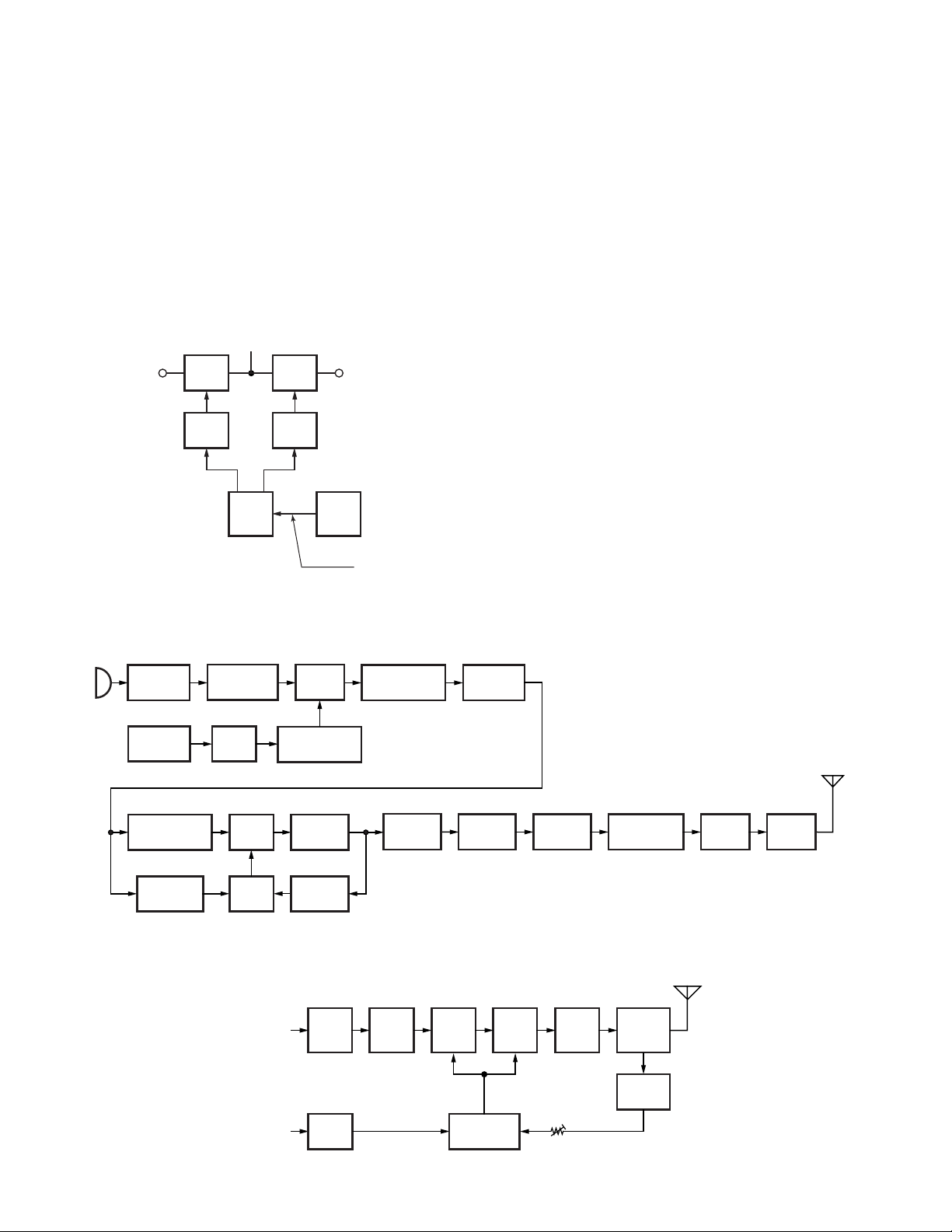
■ Unlock Circuit
During reception, the 8RC signal goes high, the 8TC signal
goes low, and Q34 turns on. Q33 turns on and a voltage is
applied to 8R. During transmission, the 8RC signal goes low,
the 8TC signal goes high and Q36 turns on. Q35 turns on and
a voltage is applied to 8T.
The CPU monitors the PLL (IC401) LD signal directly.
When the PLL is unlocked during transmission, the PLL LD
signal goes low. The CPU detects this signal and makes the
8TC signal low. When the 8TC signal goes low, no voltage is
applied to 8T, and no signal is transmitted. (See Fig. 7.)
8C
8R 8T
Q33
SW
Q34
SW
8RC
IC101
CPU
Q35
SW
Q36
SW
LD
8TC
IC401
PLL
PLL lock
: LD “H”
Fig. 7 Unlock circuit
Transmitter System
■ Outline
The transmitter circuit produces and amplifies the desired
frequency directly. It FM-modulates the carrier signal by
means of a varicap diode.
■ Power Amplifier Circuit
The transmit output signal from the VCO passes through
the transmission/reception selection diode (D409) and amplified by Q501, Q502 and Q503. The amplified signal goes to
the final amplifier (Q504) through a low-pass filter. The lowpass filter removes unwanted high-frequency harmonic components, and the resulting signal is transmitted through the
antenna terminal. (See Fig. 8.)
■ APC Circuit
The automatic transmission power control (APC) circuit
detects part of a final amplifier output with a diode (D606,
D607) and applies a voltage to IC501. IC501 compares the
APC control voltage (PC) generated by the D/A converter
(IC161) and DC amplifier (IC203) with the detection output
voltage. IC501 generates the voltage to control Q503 and
Q504 and stabilizes transmission output.
The APC circuit is configured to protect over current of
Q503 and Q504 due to fluctuations of the load at the antenna
end and to stabilize transmission output at voltage and temperature variations. (See Fig. 9.)
MIC
MIC/IDC
MIC KEY
INPUT
IC161
D/A
CONVERTER
X401
TCXO
16.8MHz
IC202IC201
SPLATTER
FILTER
IC101
CPU
Q406
VCO
PLL
IC401
D409
IC161
(PC/TVO)
IC203
SUM
AMP
IC161
D/A
CONVERTER
Q410
BUFFER
Q404
RF AMP
Q501
RF
AMP
IC203
DC
AMP
IC161
D/A
CONVERTER
IC402
1/2
DIVIDER
IC203
BUFFER
Q411
RF AMP
Q501
RF AMP
Fig. 8 Transmitter system
Q502
PRE
DRIVE
AMP
(PC)
Q503
DRIVE
AMP
IC501
CONTROL
FINAL
APC
D602,D603
Q504
AMP
VR601
D605
ANT
SW
D606
D607
Q502
PRE
DRIVE AMP
LPF
POWER
DET
ANT
Q503
DRIVE
AMP
ANT
Q504
FINAL
AMP
4
Fig. 9 APC circuit
CIRCUIT DESCRIPTION
TM-271A/271E
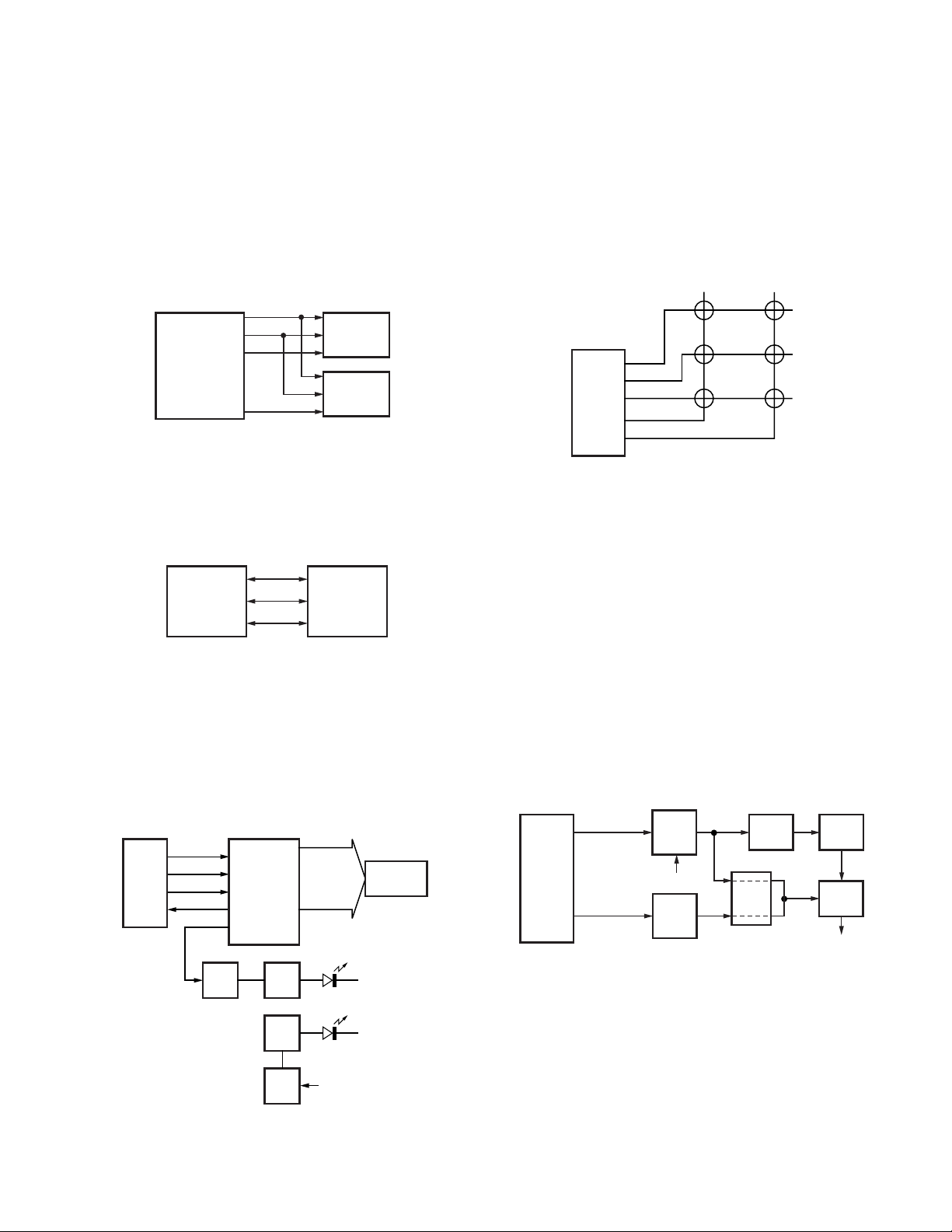
Control Circuit
The CPU carries out the following tasks (See Fig. 10.):
1) Controls the WIDE, NARROW, TX/RX outputs.
2) Adjusts the AF signal level of the AF filter (IC251) and
turns the filter select compounder on or off.
3) Controls the display unit.
4) Controls the PLL (IC401).
5) Controls the D/A converter (IC161) and adjusts the volume, modulation and transmission power.
CK
DT
IC101
CPU
LD
PLLE
Fig. 10 Control circuit
■ Memory Circuit
The transceiver has an 64k-bit EEPROM (IC66). The
EEPROM contains adjustment data. The CPU (IC101) controls the EEPROM through three serial data lines. (See Fig.
11.)
EEPCK
IC101
CPU
EEPSDT
EEPWP
Fig. 11 Memory circuit
■ Display Circuit
The CPU (IC101) controls the display LCD and LEDs.
When power is on, the LCD driver will use the BL line to control the LCD illumination and key backlight LEDs.
The brightness function is controlled by the switch Q12.
The LCD driver (IC3) and CPU (IC101) communicate through
the CE, CL, DI, DO lines. (See Fig. 12.)
CE
IC101
CPU
CL
DI
DO
BL
IC3
LCD
driver
converter
IC66
EEPROM
COM0~
COM3
SEG0~
SEG30
IC161
D/A
IC401
PLL
LCD
■ Key Matrix Circuit
The TM-271 front panel has function keys. Each of them
is connected to a cross point of a matrix of the KI1 to KI3 and
KSI to KS2 ports of the LCD driver.
The LCD driver monitors the status of the KI1 to KI3 and
KS1 to KS2 ports. If the state of one of the ports changes,
the LCD driver assumes that the key at the matrix point corresponding to that port has been pressed.
IC3
LCD
driver
KI1
KI2
KI3
KS2
KS1
FUNC
REV
MHz
(Encoder)
CALL
VFO
MR
Fig. 13 Key matrix circuit
■ Encode
The DCS and CTCSS signals are output from QT/DQT of
the CPU (IC101) and summed with the external pin DI line by
the summing amplifier (IC203) and the resulting signal goes
to the D/A converter (IC161). The DTMF signal is output from
DTMF pin of the CPU and summed with a MIC signal by the
summing amplifier (IC203), and the resulting signal goes to
the D/A converter (IC161).
The D/A converter (IC161) adjusts the MOD level and the
balance between the MOD and CTCSS/DCS levels. Part of a
CTCSS/DCS signal is summed with MOD and the resulting
signal goes to the VCOMOD pin of the VCO. This signal is
applied to a varicap diode in the VCO for direct FM modulation.
TCXO
MOD
X401
TCXO
DI
IC161
D/A
VCO
MOD
IC401
PLL
VCO
Amp
TONE
IC101
CPU
DTMF
QT/DQT
(CPU1)
DTMO
(EVOL15)
IC203
SUM
AMP
IC203
SUM
AMP
Q6
SW
Q10
SW
Q9
SW
Q12
SW
D2~D4
D19~D30
BRI
Fig. 12 Display circuit
Fig. 14 Encoder
5
TM-271A/271E
CIRCUIT DESCRIPTION
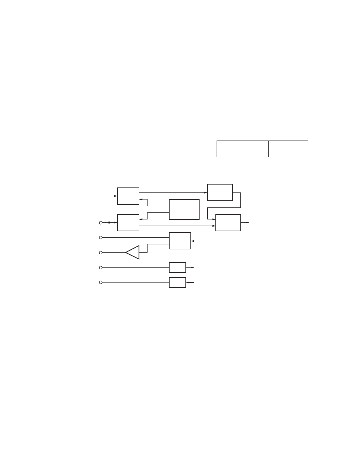
■ Decode
• CTCSS/DCS
The signal (W/NO (EVOL2)) goes to DTMF IN (pin 95) of
CPU (IC101). The CTCSS/DCS signal will pass through the
low-pass filters in the CPU (IC101) and be decoded within the
CPU (IC101). The DTMF signal will be decoded within the
CPU (IC101).
IC101
CPU
DTMF IN
95
W/NO (EVOL2)
Fig. 15 Decode
■ D/A Converter
The D/A converter (IC161) is used to adjust MO modulation, AF volume, TV voltage, FC reference voltage, and PC
POWER CONTROL voltage level.
Adjustment values are sent from the CPU as serial data.
The D/A converter has a resolution of 256 and the following
relationship is valid:
D/A output = (Vin – VDAref) / 256 x n + VDAref
Vin: Analog input
VDAref: D/A reference voltage
n: Serial data value from the microprocessor (CPU)
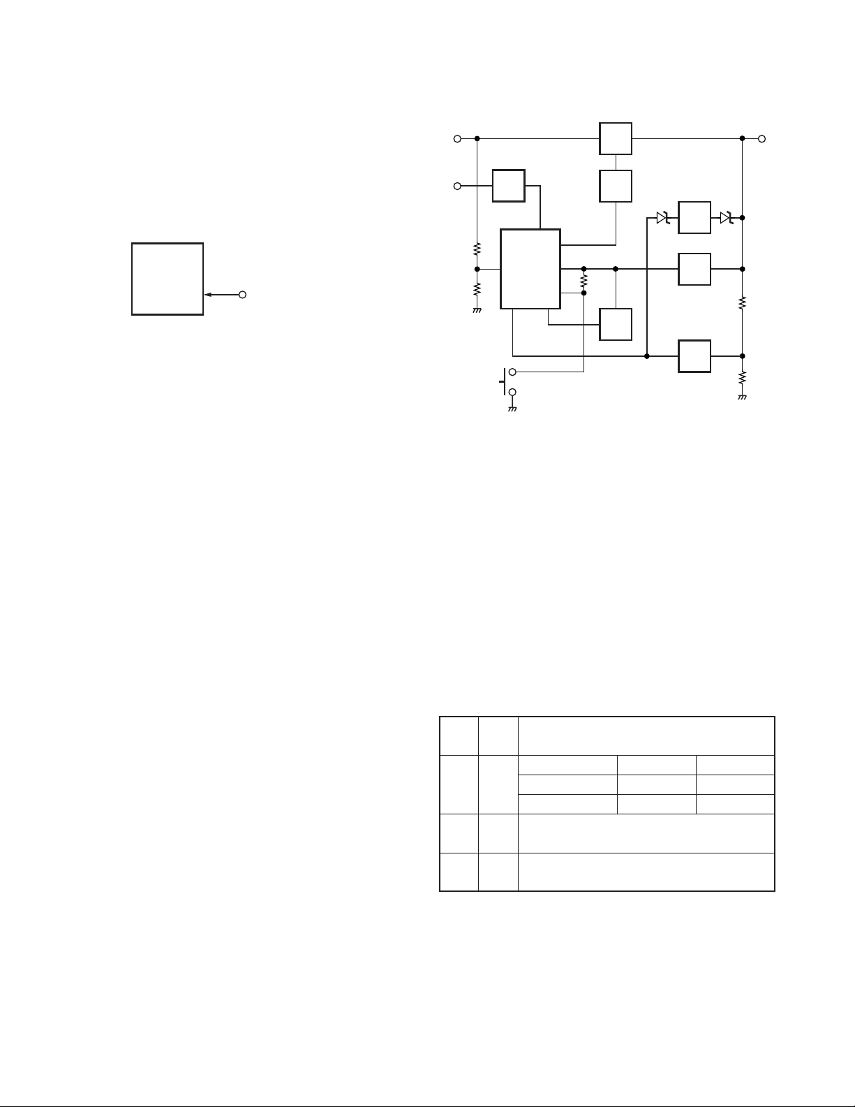
Power Supply Circuit
When the power switch on the display unit is pressed, the
power port on the display unit which is connected port 17
(POWER), goes low, then port 82 (SBC) goes high, Q32 turns
on, SB SW (Q31) turns on and power (SB) is supplied to the
radio.
When the DC power supplied to the radio, the voltage
regulator IC (IC33) supply into the CPU VDD and reset voltage
detect IC (IC34). IC34 will generate signal (RESET) in to the
reset terminal on the CPU (IC101) to carry out a power ON
reset. If DC power is less than about 9.5V, the radio is unable
to power on.
When the DC power voltage deceases from normal voltage, the INT voltage detector IC (IC35) will set to high on CPU
port 18 (INT) if B line will became less than about 9.5V. Then
CPU send to EEPROM (IC66) the backup data and go into
STOP mode.
This circuit has an overvoltage protection circuit. If a DC
voltage of 18V or higher is applied to the base of Q61, this
voltage turns Q61 on and will set to high on CPU port 18
(INT). Then CPU send to EEPROM (IC66) the backup data
and go into stop mode. (See Fig. 16.)
SB
IGN
R77R76
POWER
SW
Q71
SW
BATT
INT
IGN
IC101
CPU
POWER
RESET
SBC
5M
Q31
SW
Q32
SW
IC34
RST
5M
Q61
SW
IC33
AVR
IC35
INT
D61D62
B
R39R40
Fig. 16 Power supply circuit
Data Terminal and Peripheral Circuits
CN2 (data terminal) is the data communications terminal
on the TX/RX PCB. It handles transmission control, data input/output, and squelch signals.
There are two data communications modes : 9600bps
mode and 1200bps mode. Unlike with 1200bps AFSK, with
this type of high-speed modulation, frequency modulation is
carried out after the digital base band signals (rectangular
wave) are passed through a band limiting filter. For 9600bps
GMSK for example, compared to 4800Hz signals (nearly sine
wave signals passed through a filter), these signals have a
hissing sound like digital modulation when listened to by ear.
Different types of modulation, such as GMSK is distinguished by the type of band limiting filter.
Pin Pin Specification
No. Name
1 PKD bps switching 1200bps 9600bps
Modulation input 400mVp-p 4Vp-p
Frequency shift 3± 0.5kHz 2.2± 0.5kHz
4 PR9 Output level 500mVp-p/10kΩ
Always output during reception
5 PR1 Output level 500mVp-p/10kΩ
Not output when squelch off
Table 4 Data terminal input/output level
6
CIRCUIT DESCRIPTION
TM-271A/271E
■ Transmission Signals
Transmission modulation signals enter from PKD of the
data terminal (CN2). The path to the modulation depends on
whether communications are 1200bps or 9600bps mode.
For 1200bps mode, the transmission modulation signals
from single analog switch (IC204) pass through MIC amplifier
(IC201,202) and summing amplifier (IC203), and go to VCO
(X401) through D/A converter (IC161).
For 9600bps mode, the transmission modulation signals
from single analog switch (IC205) pass through summing
amplifier (IC303), go to TCXO (X401) and VCO through D/A
converter (IC161). (See Fig. 17.)
■ Reception Signals
PR9 is the 9600bps data communications reception output. It outputs the FM detection circuit output through an AF
filter (IC251). These signals are always output whether the
squelch is open or closed.
IC204
Analog
PKD
CN2
switch
IC205
Analog
switch
1200bps
9600bps
76
75
PR1 is the 1200bps data communications reception output. It outputs the FM detection circuit output through an AF
filter (IC251). Output is controlled with the mute switch
(Q252) according to whether squelch is open or closed. (See
Fig. 17.)
■ Squelch Signal Output Circuit
The squelch circuits is input to the TNC to prevents conflicts from occurring between simultaneous receive mode
and transmit mode traffic during packet communications
(only during 1200bps). The signal is output from pin 29 of
IC101 to the data terminal. The logic is as shown in the table
below.
SQC terminal output L : SQ CLOSE
CN2 H : SQ BUSY
IC201,202
MIC amp
IC101
CPU
IC203
Sum amp
VCO, TCXO,
D/A converter
PR9
PR1
PKS
SQC
Q252
Mute SW
IC251
AF filter
D6
D5
D/A converter
PKS (CPU) pin 30
SQC (CPU) pin 29
Fog. 17 Data terminal and peripheral circuits
7
TM-271A/271E
SEMICONDUCTOR DATA
Microprocessor : 30622MAA-B85GP (TX-RX Unit IC101)
■ Terminal Function
Pin No. Name I/O Function
1 TONE O CTCSS/DCS/Clone output
2 DTMF O DTMF/BEEP/1750Hz output
3 PLLE O PLL IC chip select
4,5 NC I
6 GND - GND.
7 CNVSS -
8 EVLLD O
9 BSHIFT O Beat shift
10 RESET - Reset
11 XOUT - X’tal (8MHz)
12 VSS - GND
13 XIN - X’tal (8MHz)
14 VCC - +5V
15 NMI - (Input only)
16 NC I
17 POWER I Power key input
18 INT I µcom stop
19 NC I
20 TX/RX O TX/RX
21 UL I PLL unlock detect
22,23 NC I
24 EEPSDT I/O EEPROM data
25 EEPCK O EEPROM clock
26 EEPWP O EEPROM write protect
27,28 NC I (Nch open drain)
29 SQC O Squelch signal output for TNC
(TxD for flash)
30 PKS I PTT input for TNC (RxD for flash)
31 CLKFLS I (GND)
32 BSYFLS O (Vcc)
33 TXD O To PC
34 RXD I From PC
35 PTT I PTT input
36~38 NC I
39 EMPFLS I/O (GND)
40~43 NC I
44 CEFLS I/O (Vcc)
45~49 NC I
50 AFM O AF mute
51 SPM O Speaker mute
52 AMPSW O AF AMP switch
Pin No. Name I/O Function
53 DT O Common data
54 CK O Common clock
55 NC I
56 DST1 I Destination 1
57~59 DST2~DST4 I Destination 2~4
60 VCC - +5V
61 NC I
62 VSS - GND
63 ADJ I For adjustment mode
64 NARROW O Wide/Narrow 2
65 WIDE O Wide/Narow
66,67 NC I
68 LCDCL O Clock for LCD
69 LCDCE O Chip enable for LCD
70 LCDDO O Output data to LCD
71 LCDDI I Input data from LCD
72 NC I
73 ENCB I Encoder input B
74 ENCA I Encoder input A
75 TNC9600 O TNC speed H : 9600, L : 1200
76 TNC1200 O TNC speed L : 9600, H : 1200
77 MICMT O MIC mute
78 NC I NC
79 8RC O 8R control
80 8TC O 8T control
81 NC I
82 SBC O Battery switch
83~85 NC I
86 CM I/O MIC key check
87 I For AMR DTMF keypad MIC
88 I For AMR DTMF keypad MIC
89 VOL I Volume encoder
90 TEMP2 I Temperature 2
91 TEMP1 I Temperature 1
92 RSSI I RSSI input
93 SQIN I Squelch input
94 AVSS - GND
95 DTMF IN I CTCSS/DCS/Clone/1050Hz input
96 VREF - +5V
97 AVCC - +5V
98~100
NC I
8

COMPONENTS DESCRIPTION
TM-271A/271E
Display Unit (X54-3450-10)
Ref. No. Parts name Description
IC3 IC LCD controller
Q6 Transistor DC switch
Q9 Transistor LCD backlit switch
Q10 Transistor Key backlit switch
Q12 Transistor Brightness function switch
D2~4 LED Key backlit
D19~30 LED LCD backlit
D31 Diode Reverse connection protection
TX-RX Unit (X57-685X-XX)
Ref. No. Parts name Description
IC31 IC Voltage regulator (8C)
IC32 IC Voltage regulator (5C)
IC33 IC Voltage regulator (5M)
IC34 IC Voltage detector (reset)
IC35 IC Voltage detector (int)
IC66 IC EEPROM
IC101 IC CPU
IC161 IC Digital potentiometer
IC201 IC MIC amplifier / IDC
IC202 IC MIC amplifier / Splatter filter
IC203 IC Buffer amplifier / SUM amplifier
/ DC amplifier / 1/2 Vcc
IC204,205
IC251 IC Audio filter
IC252 IC Audio amplifier
IC301 IC FM demodulation
IC401 IC PLL synthesizer
IC402 IC Divider (Hetero)
IC501 IC APC controller
Q31,32 Transistor
Q33,34 Transistor DC switch (8R) / Active while RX
Q35,36 Transistor DC switch (8T) / Active while TX
Q61 Transistor Over voltage detection / Active when
Q86,87 Transistor Beat shift / Active while beat shift is on
Q201 Transistor AGC / MIC mute
Q251 Transistor Buffer amplifier / RX audio
Q252,253
Q254
Q255 Transistor AF mute / Active while AMPSW is H
Q301 Transistor Noise amplifier / SQL amplifier
IC Single analog switch
DC switch (SB) / Active when power is on
PS voltage is more than 18V
FET AF mute / Active while AFM is H
Digital transistor
AF mute / Active while SPM is H
Ref. No. Parts name Description
Q302 Transistor Buffer amplifier / 16.8MHz 3rd over tone
Q351 Transistor IF amplifier
Q352 FET Mixer
Q353 FET RF amplifier / LNA
Q354 Transistor PC/TV switch
Q402,403
Q404 Transistor RF amplifier / PLL F in
Q405 FET RX VCO
Q406 FET TX VCO
Q407 FET T/R switch
Q408 Transistor T/R switch
Q410 Transistor Buffer amplifier / Output of VCO
Q411 Transistor RF amplifier / Output of VCO
Q440 Transistor Lipple filter
Q501,502
Q503 FET RF amplifier / Drive amplifier
Q504 FET RF amplifier / Final amplifier
D1 Diode Surge absorption / CM
D2 Diode Surge absorption / MIC key
D3 Diode Surge absorption / RXD
D4 Diode Surge absorption / PTT
D5 Diode Surge absorption / SQC
D6 Diode Surge absorption / PKS
D31 Diode Reverse connection protection
D32 Poly switch Current protection
D61,62 Diode Over voltage detection
D201 Diode OR gate / MIC mute, AGC
D202 Diode AGC
D251 Diode Limiter
D301 Diode Detection
D302,303
D351~354
D401 Diode Ripple filter
D402 Diode Voltage dropped
D403,404
D405,406
D407 Varicap Modulation
D408 Diode Lipple filter
D409 Diode RF switch (TX/RX)
D501,502
D503 Diode Voltage protection
D602,603
D605 Diode ANT switch
D606,607
D608 Diode Temperature compensation
Transistor Charge pump
Transistor RF amplifier / Drive stage
Diode IF switch (Wide/Narrow)
Varicap RF BPF tuning
Varicap RX VCO
Varicap TX VCO
Diode Temperature compensation
Diode ANT switch
Diode APC voltage detect
9

TM-271A/271E
PARTS LIST
✽ New Parts. indicates safety critical components.
Parts without Parts No. are not supplied.
Les articles non mentionnes dans le Parts No. ne sont pas fournis.
Teile ohne Parts No. werden nicht geliefert.
TM-271A/E
DISPLAY UNIT (X54-3450-10)
Ref. No.
Address
New
Parts No. Description
parts
Destination
TM-271A/E
11B✽ A01-2193-01 CABINET
23BA10-4048-21 CHASSIS
33A✽ A62-1088-03 PANEL ASSY
51D✽ B62-1738-10 INSTRUCTION MANUAL K,M2,M3
51D✽ B62-1738-10 INSTRUCTION MANUAL E
51D✽ B62-1739-10 INSTRUCTION MANUAL K,M2,E
51D✽ B62-1745-10 INSTRUCTION MANUAL M3
51D✽ B62-1746-10 INSTRUCTION MANUAL M4
51D✽ B62-1784-10 INSTRUCTION MANUAL E
63B✽ B72-2171-04 MODEL NAME PLATE K
63B✽ B72-2172-04 MODEL NAME PLATE M2
63B✽ B72-2173-04 MODEL NAME PLATE M3
63B✽ B72-2174-04 MODEL NAME PLATE M4
63B✽ B72-2175-04 MODEL NAME PLATE E
83BE04-0167-05 RF COAXIAL PECEPTACLE (M) K,M2,M3
83BE04-0167-05 RF COAXIAL PECEPTACLE (M) M4
93BE04-0170-05 RF COAXIAL RECEPTACLE (N) E
10 3C E30-2111-15 DC CORD ACCESSORY K,M2,M3
10 3C E30-2111-15 DC CORD ACCESSORY M4
11 3C ✽ E30-3452-05 DC CORD ACCESSORY E
12 2B ✽ E30-7501-05 TNC CABLE E
13 2B ✽ E30-7512-05 DC CORD (RADIO) K,M2,M3
13 2B ✽ E30-7512-05 DC CORD (RADIO) M4
14 2B ✽ E30-7513-05 DC CORD (RADIO) E
15 3A E37-1082-05 SPEAKER WIRE
16 2A ✽ E37-1097-05 FLAT CABLE
L : Scandinavia K : USA P : Canada
Y : PX (Far East, Hawaii) T : England E : Europe
Y : AAFES (Europe) X : Australia M :Other Areas
Ref. No.
44 3A ✽ K29-9293-03 KNOB (ENCODER)
A2BN67-2608-46 PAN HEAD SEMS SCREW
B2AN80-2010-45 PAN HEAD TAPTITE SCREW
C 2B,3B N87-2606-46 BRAZIER HEAD TAPTITE SCREW
D 1B,2B N87-2614-46 BRAZIER HEAD TAPTITE SCREW
46 3D N99-0395-05 SCREW SET ACCESSORY
48 3A T07-0739-05 SPEAKER
49 2C T91-0624-05 MICROPHONE ACCESSORY M2,M4
50 2C ✽ T91-0641-05 MICROPHONE ACCESSORY K,M3,E
Address
New
Parts No. Description
parts
nation
DISPLAY UNIT (X54-3450-10)
101 2A ✽ B11-1809-03 ILLUMINATION GUIDE (LCD)
102 2A ✽ B38-0885-05 LCD
D2-4 B30-2205-05 LED (YG)
D19-30 B30-2205-05 LED (YG)
C4 CC73GCH1H101J CHIP C 100PF J
C15,16 CC73GCH1H101J CHIP C 100PF J
C19 CK73GB1H681K CHIP C 680PF K
C22 CK73GB1H102K CHIP C 1000PF K
C24 CK73GB1C104K CHIP C 0.10UF K
C25 CK73GB1H102K CHIP C 1000PF K
C27 CK73GB1H102K CHIP C 1000PF K
C30 CK73GB1C104K CHIP C 0.10UF K
C31-33 CK73GB1H102K CHIP C 1000PF K
C34,35 CK73GB1H472K CHIP C 4700PF K
Desti-
17 3C ✽ F51-0024-05 FUSE (BLADE) (15A/32V) E
18 2B F10-2449-01 SHIELDING COVER
20 3C F51-0017-05 FUSE (6✽30) (15A) K,M2,M3
20 3C F51-0017-05 FUSE (6✽30) (15A) M4
23 2B G02-0894-04 EARTH SPRING (FINAL FET)
24 2A ✽ G10-1324-04 FIBROUS SHEET (DISPLAY UNIT)
25 3B G11-4127-14 RUBBER SHEET (CHASSIS)
26 2B G11-4240-04 RUBBER SHEET (DRIVE FET)
27 3B G13-1468-04 CUSHION (CHASSIS) K,M2,M3
27 3B G13-1468-04 CUSHION (CHASSIS) M4
28 3A G53-1525-03 PACKING (PANEL)
29 2B G53-1542-03 PACKING (PHONE JACK)
30 1B G53-1544-01 PACKING (SHIELDING COVER)
31 1A G53-1548-02 GASKET
33 2C,1D H12-3112-05 PACKING FIXTURE
34 3D H13-1190-02 CARTON BOARD
36 1D H25-2341-04 PROTECTION BAG
37 2D ✽ H52-1995-12 ITEM CARTON CASE K,M2
37 2D ✽ H52-2027-02 ITEM CARTON CASE M3
37 2D ✽ H52-2028-02 ITEM CARTON CASE M4
37 2D ✽ H52-2029-12 ITEM CARTON CASE E
39 3C J19-1584-05 MIC HOLDER ACCESSORY
40 3D J29-0662-03 BRACKET ACCESSORY
42 3A ✽ K29-9291-01 KEY TOP
43 3A ✽ K29-9292-03 KNOB (VOLUME)
10
C36 CK73GB0J105K CHIP C 1.0UF K
C38 CK73GB1H471K CHIP C 470PF K
C39,40 CK73GB1C104K CHIP C 0.10UF K
103 2A ✽ E29-1201-04 INTER CONNECTOR (LCD)
CN1 E40-6005-05 FLAT CABLE CONNECTOR
J1 E08-0877-05 MODULAR JACK
104 2A ✽ J21-8463-03 HARDWARE FIXTURE (LCD)
L1 L92-0138-05 FERRITE CHIP
CP1 R90-0724-05 MULTI-COMP 1K X4
R8 RK73GB1J102J CHIP R 1.0K J 1/16W
R10 RK73GB1J122J CHIP R 1.2K J 1/16W
R21-23 RK73GB1J103J CHIP R 10K J 1/16W
R25 RK73GB1J563J CHIP R 56K J 1/16W
R26 RK73GB1J392J CHIP R 3.9K J 1/16W
R41 RK73FB2A560J CHIP R 56 J 1/10W
R42 RK73GB1J272J CHIP R 2.7K J 1/16W
R43 RK73GB1J821J CHIP R 820 J 1/16W
R44 RK73GB1J183J CHIP R 18K J 1/16W
R45 RK73GB1J333J CHIP R 33K J 1/16W
R46 RK73GB1J101J CHIP R 100 J 1/16W
R47,48 RK73GB1J473J CHIP R 47K J 1/16W
R49,50 RK73FB2A560J CHIP R 56 J 1/10W
R51-53 R92-1252-05 CHIP R 0 OHM J 1/16W
R54 RK73FB2A560J CHIP R 56 J 1/10W
K,M2,M3,M4 : TM-271A
E: TM-271E

PARTS LIST
Ref. No.
R55 R92-1252-05 CHIP R 0 OHM J 1/16W
VR1 ✽ R31-0646-05 VARIABLE RESISTOR
D31 1SS355 DIODE
IC3 ✽ LC75854W MOS IC
IC3 PT6554LQ MOS IC
Q6 KRC102S DIGITAL TRANSISTOR
Q9 2SB1132(Q,R) TRANSISTOR
Q10 KRA225S DIGITAL TRANSISTOR
Q12 UMG3N TRANSISTOR
S1 ✽ W02-3665-05 ENCODER
0-10 : K 0-21 : M2 0-22 : M3 0-23 : M4 2-71 : E
C10 CK73GB1H102K CHIP C 1000PF K
C13-20 CK73GB1H471K CHIP C 470PF K
C28 CK73GB1H221K CHIP C 220PF K
C29 CK73GB1H471K CHIP C 470PF K
C30 CK73GB1H102K CHIP C 1000PF K
Address
New
parts
Parts No. Description
TX-RX UNIT (X57-685X-XX)
Desti-
nation
TM-271A/271E
DISPLAY UNIT (X54-3450-10)
TX-RX UNIT (X57-685X-XX)
Ref. No.
C206 CK73GB1H681K CHIP C 680PF K E
C207 CK73GB1C223K CHIP C 0.022UF K K,M2,M3
C207 CK73GB1C223K CHIP C 0.022UF K M4
C207 CK73GB1C393K CHIP C 0.039UF K E
C208 CK73GB1H103K CHIP C 0.010UF K
C209 CC73GCH1H680J CHIP C 68PF J
C210 CK73GB1C104K CHIP C 0.10UF K
C211 CK73GB1H821K CHIP C 820PF K
C212 CK73GB1H122K CHIP C 1200PF K
C213 CK73GB1H332K CHIP C 3300PF K
C214 CC73GCH1H151J CHIP C 150PF J
C215 CK73GB1C104K CHIP C 0.10UF K
C216 CC73GCH1H390J CHIP C 39PF J
C217,218 C92-0560-05 CHIP-TAN 10UF 6.3WV
C220 C92-0507-05 CHIP-TAN 4.7UF 6.3WV
C222 CK73GB1C104K CHIP C 0.10UF K
C225 C92-0004-05 CHIP-TAN 1.0UF 16WV
C226 CK73GB1H472K CHIP C 4700PF K
C227 CK73GB1E103K CHIP C 0.010UF K
C228 C92-0560-05 CHIP-TAN 10UF 6.3WV
Address
New
Parts No. Description
parts
Destination
C33 CK73GB1H102K CHIP C 1000PF K
C34 ✽ CE04EQ1E331M ELECTRO 330UF 25WV
C35-38 CK73GB1H102K CHIP C 1000PF K
C39,40 CK73GB1C104K CHIP C 0.10UF K
C41 C92-0795-05 CHIP-TAN 22UF 10WV
C42 CK73GB1H103K CHIP C 0.010UF K
C43-45 C92-0795-05 CHIP-TAN 22UF 10WV
C49,50 CK73GB1H103K CHIP C 0.010UF K
C51 C92-0589-05 CHIP-TAN 47UF 6.3WV
C52,53 CK73GB1H102K CHIP C 1000PF K
C54,55 CK73GB1C104K CHIP C 0.10UF K
C56 CK73GB1H102K CHIP C 1000PF K
C61 CK73GB1H102K CHIP C 1000PF K
C66 CK73GB1H102K CHIP C 1000PF K
C82 CK73GB1H102K CHIP C 1000PF K
C83 CK73GB1C104K CHIP C 0.10UF K
C87 CC73GCH1H030C CHIP C 3.0PF C
C88,89 CC73GCH1H040C CHIP C 4.0PF C
C90 CC73GCH1H030C CHIP C 3.0PF C
C97,98 CK73GB1H102K CHIP C 1000PF K
C101 CK73GB1H102K CHIP C 1000PF K
C102 CK73GB1C104K CHIP C 0.10UF K
C104 CK73GB1C104K CHIP C 0.10UF K
C128 CK73GB1H102K CHIP C 1000PF K
C151 CK73GB1H182K CHIP C 1800PF K
C152 CK73GB1H392K CHIP C 3900PF K
C161 CK73GB1H102K CHIP C 1000PF K
C162 C92-0507-05 CHIP-TAN 4.7UF 6.3WV
C163 CK73GB1H102K CHIP C 1000PF K
C164 C92-0560-05 CHIP-TAN 10UF 6.3WV
C230 CK73GB1C104K CHIP C 0.10UF K
C231,232 CK73GB1H102K CHIP C 1000PF K
C233 C92-0507-05 CHIP-TAN 4.7UF 6.3WV
C235 CK73GB1A105K CHIP C 1.0UF K
C249 C92-0507-05 CHIP-TAN 4.7UF 6.3WV
C250 CK73GB1C104K CHIP C 0.10UF K
C251 C92-0714-05 CHIP-TAN 4.7UF 6.3WV
C252 CC73GCH1H390J CHIP C 39PF J
C253,254 CK73GB1A224K CHIP C 0.22UF K
C255 CK73GB1H822K CHIP C 8200PF K
C256 CK73GB1E183K CHIP C 0.018UF K
C257 CK73GB1C393K CHIP C 0.039UF K
C258-261 CK73GB1H103J CHIP C 0.010UF J
C262 CK73GB1H102K CHIP C 1000PF K
C263,264 CK73GB1C333K CHIP C 0.033UF K
C265 CK73GB1C104K CHIP C 0.10UF K
C266 CK73GB1A105K CHIP C 1.0UF K
C267 CK73GB1A474K CHIP C 0.47UF K
C268 CK73GB1A105K CHIP C 1.0UF K
C270 C92-0507-05 CHIP-TAN 4.7UF 6.3WV
C271 CK73GB1H122K CHIP C 1200PF K
C272 CK73GB1H102K CHIP C 1000PF K
C273 CK73GB1A105K CHIP C 1.0UF K
C274 CK73FB1C224K CHIP C 0.22UF K
C275 CK73GB1A105K CHIP C 1.0UF K
C276,277 CK73GB1H102K CHIP C 1000PF K
C278 CK73GB1C104K CHIP C 0.10UF K
C279 C92-0516-05 CHIP-TAN 4.7UF 16WV
C280 C92-0040-05 CHIP-ELE 47UF 16WV
C281 CK73GB1H102K CHIP C 1000PF K
C165 CK73GB1A105K CHIP C 1.0UF K
C201 CK73GB1C104K CHIP C 0.10UF K
C202 CK73GB1H102K CHIP C 1000PF K
C203 CK73GB1C273K CHIP C 0.027UF K K,M2,M3
C203 CK73GB1C273K CHIP C 0.027UF K M4
C203 CK73GB1C473K CHIP C 0.047UF K E
C204 C92-0514-05 CHIP-TAN 2.2UF 10WV
C205 CK73GB1C104K CHIP C 0.10UF K
C206 CK73GB1H102K CHIP C 1000PF K K,M2,M3
C206 CK73GB1H102K CHIP C 1000PF K M4
K,M2,M3,M4 : TM-271A
E: TM-271E
C282 ✽ CE04EQ1E331M ELECTRO 330UF 25WV
C283 CK73GB1H102K CHIP C 1000PF K
C301 C92-0507-05 CHIP-TAN 4.7UF 6.3WV
C302 CK73GB1H102K CHIP C 1000PF K
C303 CK73GB1H472K CHIP C 4700PF K
C304,305 CC73GCH1H331J CHIP C 330PF J
C306 CK73GB1H102K CHIP C 1000PF K
C307 CK73GB1E223K CHIP C 0.022UF K
C308 CK73GB1H102K CHIP C 1000PF K
C309 CK73GB1E223K CHIP C 0.022UF K
11

TM-271A/271E
TX-RX UNIT (X57-685X-XX)
Ref. No.
C310 CK73FB1C334K CHIP C 0.33UF K
C311,312 CK73GB1C104K CHIP C 0.10UF K
C313 C92-0662-05 CHIP-TAN 15UF 6.3WV
C314 CK73GB1H103K CHIP C 0.010UF K
C315-318 CK73GB1C104K CHIP C 0.10UF K
Address
New
Parts No. Description
parts
PARTS LIST
Destination
Ref. No.
C425 C92-0001-05 CHIP C 0.1UF 35WV
C426 CC73GCH1H300J CHIP C 30PF J
C427 CC73GCH1H080B CHIP C 8.0PF B
C428 CK73GB1H471K CHIP C 470PF K
C429 CC73GCH1H010B CHIP C 1.0PF B
Address
New
Parts No. Description
parts
Desti-
nation
C319 CK73GB1H102K CHIP C 1000PF K
C321 CC73GCH1H680J CHIP C 68PF J
C322 CC73GCH1H560J CHIP C 56PF J
C323 CC73GCH1H271J CHIP C 270PF J
C324 CK73GB1H103K CHIP C 0.010UF K
C326 CK73GB1H103K CHIP C 0.010UF K
C350 CK73GB1H471K CHIP C 470PF K
C351 CC73GCH1H330J CHIP C 33PF J
C353 CK73GB1H103K CHIP C 0.010UF K
C354 CC73GCH1H4R5B CHIP C 4.5PF B
C355 CC73GCH1H180J CHIP C 18PF J
C356 CC73GCH1H030B CHIP C 3.0PF B
C357 CK73GB1H103K CHIP C 0.010UF K
C358 CK73GB1H102K CHIP C 1000PF K
C359 CC73GCH1H080B CHIP C 8.0PF B
C360-362 CK73GB1H102K CHIP C 1000PF K
C363 CK73GB1H103K CHIP C 0.010UF K
C364 CK73GB1H102K CHIP C 1000PF K
C366 CK73GB1C104K CHIP C 0.10UF K
C367 CC73GCH1H151J CHIP C 150PF J
C368 CC73GCH1H270J CHIP C 27PF J
C369 CC73GCH1H030B CHIP C 3.0PF B
C370 CK73GB1H102K CHIP C 1000PF K
C371 CC73GCH1H020B CHIP C 2.0PF B
C372 CK73GB1H102K CHIP C 1000PF K
C373 CC73GCH1H060B CHIP C 6.0PF B
C374 CC73GCH1H270J CHIP C 27PF J
C375-379 CK73GB1H102K CHIP C 1000PF K
C380 CC73GCH1H101J CHIP C 100PF J
C381 CC73GCH1H4R5B CHIP C 4.5PF B
C430 CC73GCH1H4R5B CHIP C 4.5PF B
C431 CC73GCH1H050B CHIP C 5.0PF B
C432 CC73GCH1H0R3B CHIP C 0.3PF B
C434 CC73GCH1H151J CHIP C 150PF J
C435 CC73GCH1H100C CHIP C 10PF C
C436 CC73GCH1HR75B CHIP C 0.75PF B
C437 CK73GB1H471K CHIP C 470PF K
C438 CC73GCH1H0R5B CHIP C 0.5PF B
C439 CC73GCH1H100C CHIP C 10PF C
C440 CC73GCH1H110G CHIP C 11PF G
C441 CC73GCH1H0R5B CHIP C 0.5PF B
C442 C92-0560-05 CHIP-TAN 10UF 6.3WV
C444 CK73GB1H471K CHIP C 470PF K
C448,449 CK73GB1H471K CHIP C 470PF K
C450 C92-0795-05 CHIP-TAN 22UF 10WV
C451,452 CK73GB1H471K CHIP C 470PF K
C453 CK73GB1H221K CHIP C 220PF K
C454 CC73GCH1H060B CHIP C 6.0PF B
C455 CC73GCH1H030B CHIP C 3.0PF B
C456 CC73GCH1H020B CHIP C 2.0PF B
C457 CK73GB1H102K CHIP C 1000PF K
C458 CK73GB1H221K CHIP C 220PF K
C459 CK73GB1H102K CHIP C 1000PF K
C460 CC73GCH1H180J CHIP C 18PF J
C461 CK73GB1H102K CHIP C 1000PF K
C462 CC73GCH1H100C CHIP C 10PF C
C463,464 CK73GB1H102K CHIP C 1000PF K
C465 CC73GCH1H220J CHIP C 22PF J
C466 CC73GCH1H101J CHIP C 100PF J
C467 CK73GB1H102K CHIP C 1000PF K
C382 CC73GCH1H270J CHIP C 27PF J
C383 CK73GB1H102K CHIP C 1000PF K
C384 CC73GCH1H020B CHIP C 2.0PF B
C385 CC73GCH1H080B CHIP C 8.0PF B
C386 CC73GCH1H360J CHIP C 36PF J
C387 CK73GB1H102K CHIP C 1000PF K
C388 CC73GCH1H070B CHIP C 7.0PF B
C389 CK73GB1H102K CHIP C 1000PF K
C390 CC73GCH1H090B CHIP C 9.0PF B
C391 CC73GCH1H160G CHIP C 16PF G
C400 CK73GB1C104K CHIP C 0.10UF K
C401-403 CC73GCH1H101J CHIP C 100PF J
C404 C92-0662-05 CHIP-TAN 15UF 6.3WV
C406 CK73GB1H102K CHIP C 1000PF K
C408 CC73GCH1H220J CHIP C 22PF J
C409 CK73GB1C104K CHIP C 0.10UF K
C410 C92-0560-05 CHIP-TAN 10UF 6.3WV
C411 CK73GB1C104K CHIP C 0.10UF K
C412 C92-0560-05 CHIP-TAN 10UF 6.3WV
C413 CK73GB1H103K CHIP C 0.010UF K
C414 CK73GB1C104K CHIP C 0.10UF K
C416-418 CK73GB1H102K CHIP C 1000PF K
C421,422 CK73GB1H471K CHIP C 470PF K
C423 C92-0555-05 CHIP-TAN 0.047UF 35WV
C424 C92-0004-05 CHIP-TAN 1.0UF 16WV
12
C468 CK73GB1H221K CHIP C 220PF K
C471 CC73GCH1H100C CHIP C 10PF C
C473-476 CK73GB1H102K CHIP C 1000PF K
C501,502 CK73GB1H102K CHIP C 1000PF K
C503 CC73GCH1H101J CHIP C 100PF J
C504-507 CK73GB1H102K CHIP C 1000PF K
C509 CC73GCH1H150J CHIP C 15PF J
C510 CC73GCH1H080B CHIP C 8.0PF B
C511-514 CK73GB1H102K CHIP C 1000PF K
C515 CC73GCH1H270J CHIP C 27PF J
C516 CK73GB1H821K CHIP C 820PF K
C517 CC73GCH1H030B CHIP C 3.0PF B
C518 CC73GCH1H330J CHIP C 33PF J
C519 CC73GCH1H820J CHIP C 82PF J
C522 CK73FB1H102K CHIP C 1000PF K
C525 CK73GB1H102K CHIP C 1000PF K
C526 CK73GB1H681K CHIP C 680PF K
C527 CK73GB1H102K CHIP C 1000PF K
C528 CK73GB1H221K CHIP C 220PF K
C529 CK73FB1H102K CHIP C 1000PF K
C530 CK73FB1C474K CHIP C 0.47UF K
C531 C92-0719-05 CHIP-TAN 47UF 25WV
C533 C93-0572-05 CHIP C 100PF J
C536 CK73FB1H102K CHIP C 1000PF K
C541,542 CM73F2H120J CHIP C 12PF J
K,M2,M3,M4 : TM-271A
E: TM-271E

Ref. No.
C543,544 CM73F2H150J CHIP C 15PF J
C545 C93-0603-05 CHIP C 1000PF K
C546 CK73FB1C474K CHIP C 0.47UF K
C549 CM73F2H221J CHIP C 220PF J
C550 CM73F2H680J CHIP C 68PF J
Address
New
parts
Parts No. Description
PARTS LIST
Desti-
nation
Ref. No.
L418 L41-3375-06 SMALL FIXED INDUCTOR
L419 L41-1085-06 SMALL FIXED INDUCTOR
L420 L41-1585-06 SMALL FIXED INDUCTOR
L421 L41-1085-06 SMALL FIXED INDUCTOR
L422 L40-5675-92 SMALL FIXED INDUCTOR (56NH)
Address
TM-271A/271E
New
Parts No. Description
parts
TX-RX UNIT (X57-685X-XX)
Destination
C552 C93-0564-05 CHIP C 22PF J
C553 C93-0553-05 CHIP C 3.0PF C
C554 C93-0603-05 CHIP C 1000PF K
C555 C93-0555-05 CHIP C 5.0PF C
C556 C93-0603-05 CHIP C 1000PF K
C557,558 CK73GB1H103K CHIP C 0.010UF K
C559 CK73GB1C104K CHIP C 0.10UF K
C560 CK73GB1H102K CHIP C 1000PF K
C574 CK73GB1H102K CHIP C 1000PF K
C576 CK73GB1H221K CHIP C 220PF K
C602 C93-0561-05 CHIP C 12PF J
C603 C93-0603-05 CHIP C 1000PF K
C605 C93-0562-05 CHIP C 15PF J
C606 CC73GCH1H0R5B CHIP C 0.5PF B
C607 CC73GCH1H020B CHIP C 2.0PF B
C608 C93-0565-05 CHIP C 27PF J
C610 CC73GCH1H0R5B CHIP C 0.5PF B
C611 CC73GCH1H020B CHIP C 2.0PF B
C613 C93-0565-05 CHIP C 27PF J
C614 C93-0553-05 CHIP C 3.0PF C E
C615 C93-0564-05 CHIP C 22PF J
C616,617 CK73GB1H102K CHIP C 1000PF K
C623 C93-0553-05 CHIP C 3.0PF C
TC401 C05-0399-05 CERAMIC TRIMMER (6PF)
TC402 C05-0245-05 CERAMIC TRIMMER (10PF)
- E11-0425-05 3.5D PHONE JACK (3P)
- E37-1127-05 PROCESSED LEAD WIRE
CN1 E40-6268-05 FLAT CABLE CONNECTOR
CN2 E40-5705-05 PIN ASSY
CN5 E40-3246-05 PIN ASSY
F1 F53-0246-05 FUSE (4.0A/32V)
F501 F53-0108-05 FUSE (1.8A/50V)
CF301 L72-0993-05 CERAMIC FILTER
CF302 L72-0999-05 CERAMIC FILTER
L101 L92-0443-05 FERRITE CHIP
L201 L92-0443-05 FERRITE CHIP
L301 L34-4554-05 COIL
L302 L41-3385-08 SMALL FIXED INDUCTOR
L303,304 L40-3381-86 SMALL FIXED INDUCTOR (0.33UH)
L351 L41-8285-08 SMALL FIXED INDUCTOR
L352 L41-5685-08 SMALL FIXED INDUCTOR
L354-356 L34-4612-05 AIR-CORE COIL
L357 L34-4610-05 AIR-CORE COIL
L401 L92-0443-05 FERRITE CHIP
L403 L41-1005-08 SMALL FIXED INDUCTOR
L404 L92-0442-05 FERRITE CHIP
L405 L92-0443-05 FERRITE CHIP
L406,407 L40-2785-92 SMALL FIXED INDUCTOR (270NH)
L408 L40-3378-67 SMALL FIXED INDUCTOR (33NH)
L409,410 L40-2702-86 SMALL FIXED INDUCTOR (27UH)
L411,412 L40-2785-92 SMALL FIXED INDUCTOR (270NH)
L413 L40-4778-67 SMALL FIXED INDUCTOR (47NH)
L414,415 L40-2702-86 SMALL FIXED INDUCTOR (27UH)
L416,417 L92-0443-05 FERRITE CHIP
K,M2,M3,M4 : TM-271A
E: TM-271E
L423 L92-0443-05 FERRITE CHIP
L501,502 L41-6875-08 SMALL FIXED INDUCTOR
L503,504 L41-2775-06 SMALL FIXED INDUCTOR
L505 L34-4645-05 AIR-CORE COIL
L506 L34-4693-05 AIR-CORE COIL
L507 L34-4732-05 AIR-CORE COIL
L508 L34-4669-05 AIR-CORE COIL
L509 L34-4667-05 AIR-CORE COIL
L601 ✽ L34-4737-05 AIR-CORE COIL
L602-604 ✽ L34-4736-05 AIR-CORE COIL
L605 L34-4667-05 AIR-CORE COIL
X86 ✽ L78-1409-05 RESONATOR (8.00MHZ)
X401 ✽ L77-1944-05 TCXO (16.8MHZ)
XF351 L71-0620-05 MCF (49.95MHZ)
R1 R92-1252-05 CHIP R 0 OHM J 1/16W
R2,3 RK73GB1J101J CHIP R 100 J 1/16W
R4-8 RK73GB1J102J CHIP R 1.0K J 1/16W
R31 RK73GB1J472J CHIP R 4.7K J 1/16W
R32 R92-1215-05 CHIP R 470 J 1/2W
R33 RK73GB1J473J CHIP R 47K J 1/16W
R34 RK73GB1J472J CHIP R 4.7K J 1/16W
R35 RK73GB1J473J CHIP R 47K J 1/16W
R36 RK73GB1J152J CHIP R 1.5K J 1/16W
R37 R92-1252-05 CHIP R 0 OHM J 1/16W
R38 RK73GB1J334J CHIP R 330K J 1/16W
R39 RK73GB1J474J CHIP R 470K J 1/16W
R40 RK73GB1J394J CHIP R 390K J 1/16W
R41 RK73GB1J334J CHIP R 330K J 1/16W
R61 RK73GB1J471J CHIP R 470 J 1/16W
R62,63 R92-1252-05 CHIP R 0 OHM J 1/16W
R70 RK73GB1J473J CHIP R 47K J 1/16W
R81 RK73GB1J473J CHIP R 47K J 1/16W
R82 R92-1252-05 CHIP R 0 OHM J 1/16W
R86 R92-1252-05 CHIP R 0 OHM J 1/16W
R87 RK73GB1J102J CHIP R 1.0K J 1/16W
R91,92 RK73GB1J102J CHIP R 1.0K J 1/16W
R93 RK73GB1J682J CHIP R 6.8K J 1/16W
R94 RK73GB1J103J CHIP R 10K J 1/16W
R101,102 RK73GB1J473J CHIP R 47K J 1/16W
R103-106 RK73GB1J102J CHIP R 1.0K J 1/16W
R109 RK73GB1J152J CHIP R 1.5K J 1/16W
R110 RK73GB1J473J CHIP R 47K J 1/16W
R111 RK73GB1J102J CHIP R 1.0K J 1/16W
R114 RK73GB1J473J CHIP R 47K J 1/16W
R118 R92-1252-05 CHIP R 0 OHM J 1/16W
R119 R92-0670-05 CHIP R 0 OHM K,M3,M4
R119 R92-0670-05 CHIP R 0 OHM E
R120 R92-1252-05 CHIP R 0 OHM J 1/16W M4
R120-123 R92-1252-05 CHIP R 0 OHM J 1/16W K
R121-123 R92-1252-05 CHIP R 0 OHM J 1/16W E
R122,123 R92-1252-05 CHIP R 0 OHM J 1/16W M2,M3,M4
R124-127 RK73GB1J473J CHIP R 47K J 1/16W
R151 RK73GB1J103J CHIP R 10K J 1/16W
R152 RK73GB1J472J CHIP R 4.7K J 1/16W
13

TM-271A/271E
TX-RX UNIT (X57-685X-XX)
Ref. No.
R161 RK73GB1J122J CHIP R 1.2K J 1/16W
R162 RK73GB1J152J CHIP R 1.5K J 1/16W
R164-166 RK73GB1J102J CHIP R 1.0K J 1/16W
R200 RK73GB1J681J CHIP R 680 J 1/16W
R203 RK73GB1J104J CHIP R 100K J 1/16W
Address
New
Parts No. Description
parts
PARTS LIST
Destination
Ref. No.
R271 RK73GB1J332J CHIP R 3.3K J 1/16W
R272 RK73GB1J392J CHIP R 3.9K J 1/16W
R273 RK73GB1J123J CHIP R 12K J 1/16W
R274,275 RK73GB1J153J CHIP R 15K J 1/16W
R276 RK73GB1J473J CHIP R 47K J 1/16W
Address
New
Parts No. Description
parts
Desti-
nation
R204 RK73GB1J103J CHIP R 10K J 1/16W E
R204 RK73GB1J183J CHIP R 18K J 1/16W K,M2,M3
R204 RK73GB1J183J CHIP R 18K J 1/16W M4
R205 RK73GB1J821J CHIP R 820 J 1/16W
R206 RK73GB1J101J CHIP R 100 J 1/16W
R207 RK73GB1J105J CHIP R 1.0M J 1/16W E
R207 RK73GB1J754J CHIP R 750K J 1/16W K,M2,M3
R207 RK73GB1J754J CHIP R 750K J 1/16W M4
R208 RK73GB1J152J CHIP R 1.5K J 1/16W
R209 RK73GB1J244J CHIP R 240K J 1/16W
R210 RK73GB1J183J CHIP R 18K J 1/16W
R211,212 RK73GB1J823J CHIP R 82K J 1/16W
R213 RK73GB1J334J CHIP R 330K J 1/16W
R214,215 RK73GB1J683J CHIP R 68K J 1/16W
R216 RK73GB1J274J CHIP R 270K J 1/16W
R217 RK73GB1J224J CHIP R 220K J 1/16W
R218 RK73GB1J823J CHIP R 82K J 1/16W
R219 RK73GB1J124J CHIP R 120K J 1/16W
R220,221 RK73GH1J153D CHIP R 15K D 1/16W
R222 RK73GB1J103J CHIP R 10K J 1/16W
R224 RK73GB1J561J CHIP R 560 J 1/16W
R225 RK73GB1J154J CHIP R 150K J 1/16W
R226 RK73GB1J104J CHIP R 100K J 1/16W
R227 RK73GB1J223J CHIP R 22K J 1/16W
R228 RK73GB1J103J CHIP R 10K J 1/16W
R229 RK73GB1J684J CHIP R 680K J 1/16W
R230 RK73GB1J224J CHIP R 220K J 1/16W
R231 RK73GB1J124J CHIP R 120K J 1/16W
R232 RK73GB1J912J CHIP R 9.1K J 1/16W
R233 RK73GB1J682J CHIP R 6.8K J 1/16W
R277 RK73GB1J683J CHIP R 68K J 1/16W
R278 RK73GB1J123J CHIP R 12K J 1/16W
R279 RK73GB1J472J CHIP R 4.7K J 1/16W
R280 RK73GB1J391J CHIP R 390 J 1/16W
R281 R92-0670-05 CHIP R 0 OHM
R301,302 RK73GB1J472J CHIP R 4.7K J 1/16W
R303 RK73GB1J223J CHIP R 22K J 1/16W
R304 RK73GB1J472J CHIP R 4.7K J 1/16W
R305 RK73GB1J182J CHIP R 1.8K J 1/16W
R306 RK73GB1J274J CHIP R 270K J 1/16W
R308 RK73GB1J334J CHIP R 330K J 1/16W
R309 RK73GB1J332J CHIP R 3.3K J 1/16W
R310 RK73GB1J102J CHIP R 1.0K J 1/16W
R311 RK73GB1J333J CHIP R 33K J 1/16W
R312 RK73GB1J473J CHIP R 47K J 1/16W
R313 RK73GB1J104J CHIP R 100K J 1/16W
R314 RK73GB1J222J CHIP R 2.2K J 1/16W
R315 RK73GB1J183J CHIP R 18K J 1/16W
R316 RK73GB1J223J CHIP R 22K J 1/16W
R317-320 RK73GB1J103J CHIP R 10K J 1/16W
R321 RK73GB1J223J CHIP R 22K J 1/16W
R322 RK73GB1J101J CHIP R 100 J 1/16W
R323 RK73GB1J124J CHIP R 120K J 1/16W
R324 R92-1252-05 CHIP R 0 OHM J 1/16W
R325 RK73GB1J333J CHIP R 33K J 1/16W
R349 RK73GB1J473J CHIP R 47K J 1/16W
R350 RK73GB1J273J CHIP R 27K J 1/16W
R351 RK73GB1J471J CHIP R 470 J 1/16W
R352 RK73GB1J101J CHIP R 100 J 1/16W
R353 RK73GB1J104J CHIP R 100K J 1/16W
R234 R92-1252-05 CHIP R 0 OHM J 1/16W
R236 RK73GB1J103J CHIP R 10K J 1/16W
R237 R92-1252-05 CHIP R 0 OHM J 1/16W
R246 RK73GB1J154J CHIP R 150K J 1/16W
R247 RK73GB1J124J CHIP R 120K J 1/16W
R248 RK73GB1J562J CHIP R 5.6K J 1/16W
R249 RK73GB1J153J CHIP R 15K J 1/16W
R250 RK73GB1J123J CHIP R 12K J 1/16W
R251 RK73GB1J473J CHIP R 47K J 1/16W
R252 RK73GB1J474J CHIP R 470K J 1/16W
R253 R92-1252-05 CHIP R 0 OHM J 1/16W
R254 RK73GB1J272J CHIP R 2.7K J 1/16W
R255,256 RK73GB1J562J CHIP R 5.6K J 1/16W
R257 RK73GB1J105J CHIP R 1.0M J 1/16W
R258 RK73GB1J272J CHIP R 2.7K J 1/16W
R259 RK73GB1J123J CHIP R 12K J 1/16W
R260 RK73GB1J224J CHIP R 220K J 1/16W
R261 RK73GB1J124J CHIP R 120K J 1/16W
R262 RK73GB1J183J CHIP R 18K J 1/16W
R263 RK73GH1J913D CHIP R 91K D 1/16W
R264 RK73GH1J124D CHIP R 120K D 1/16W
R265 RK73GH1J562D CHIP R 5.6K D 1/16W
R266 RK73GB1J562J CHIP R 5.6K J 1/16W
R268 RK73GB1J102J CHIP R 1.0K J 1/16W
R269 RK73GB1J393J CHIP R 39K J 1/16W
14
R354 RK73GB1J331J CHIP R 330 J 1/16W
R355 RK73GB1J471J CHIP R 470 J 1/16W
R356 RK73GB1J102J CHIP R 1.0K J 1/16W
R358 RK73GB1J221J CHIP R 220 J 1/16W
R359 RK73GB1J224J CHIP R 220K J 1/16W
R360 RK73GB1J474J CHIP R 470K J 1/16W
R361 RK73GB1J181J CHIP R 180 J 1/16W
R362 RK73GB1J474J CHIP R 470K J 1/16W
R363 RK73GB1J334J CHIP R 330K J 1/16W
R364 R92-1252-05 CHIP R 0 OHM J 1/16W
R365 RK73GB1J104J CHIP R 100K J 1/16W
R366 RK73GB1J471J CHIP R 470 J 1/16W
R367 RK73GB1J101J CHIP R 100 J 1/16W
R368 RK73GB1J104J CHIP R 100K J 1/16W
R369 R92-1252-05 CHIP R 0 OHM J 1/16W
R370 RK73GB1J560J CHIP R 56 J 1/16W
R371 RK73GB1J393J CHIP R 39K J 1/16W
R372,373 RK73GB1J473J CHIP R 47K J 1/16W
R374 RK73GB1J273J CHIP R 27K J 1/16W
R375,376 RK73GB1J104J CHIP R 100K J 1/16W
R379 RK73GB1J104J CHIP R 100K J 1/16W
R401-403 RK73GB1J102J CHIP R 1.0K J 1/16W
R404 RK73GB1J103J CHIP R 10K J 1/16W
R406 RK73GB1J103J CHIP R 10K J 1/16W
R407 RK73GB1J152J CHIP R 1.5K J 1/16W
K,M2,M3,M4 : TM-271A
E: TM-271E
 Loading...