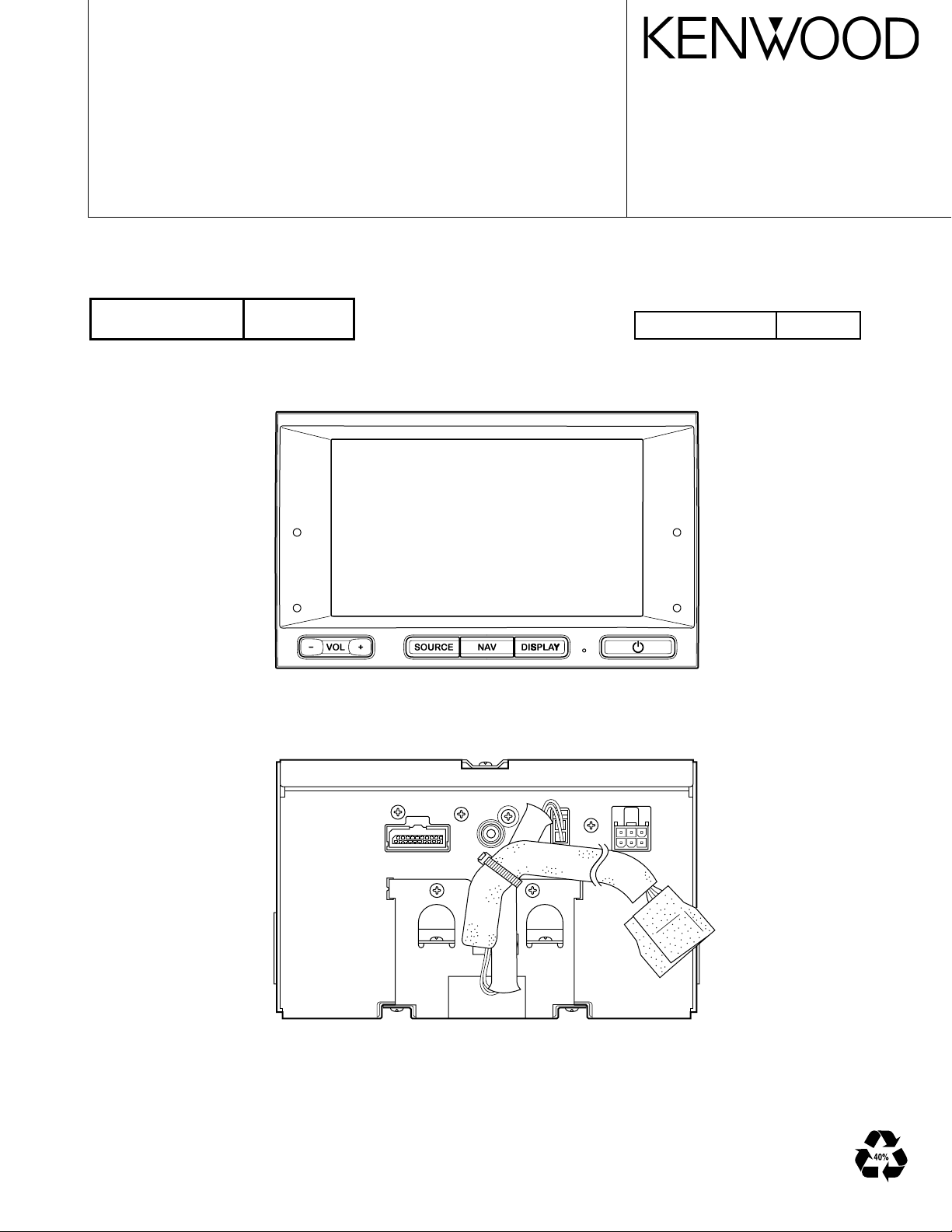
Kenwood SVT-M700 Service Manual

6.5 INCHES TV MONITOR
SVT-M700
SERVICE MANUAL
SAAB GENUINE
© 2002-9 PRINTED IN JAPAN
B51-7977-00 (N) 1864
Destination Europe
GENUINE NUMBER
55 21 372

SVT-M700
V IN
J2
(X14- )
J3
to STC-700
NAVI SYNC
NR
NG
NB
V GND
M REQ C
M REQ H
M DATA
M CLK
M CON
RST
MUTE
RX
TX
J4
to W02
REMO
ILL
J1
to BAT
BU
ILL-CONT
GND
PARK
(W02- )
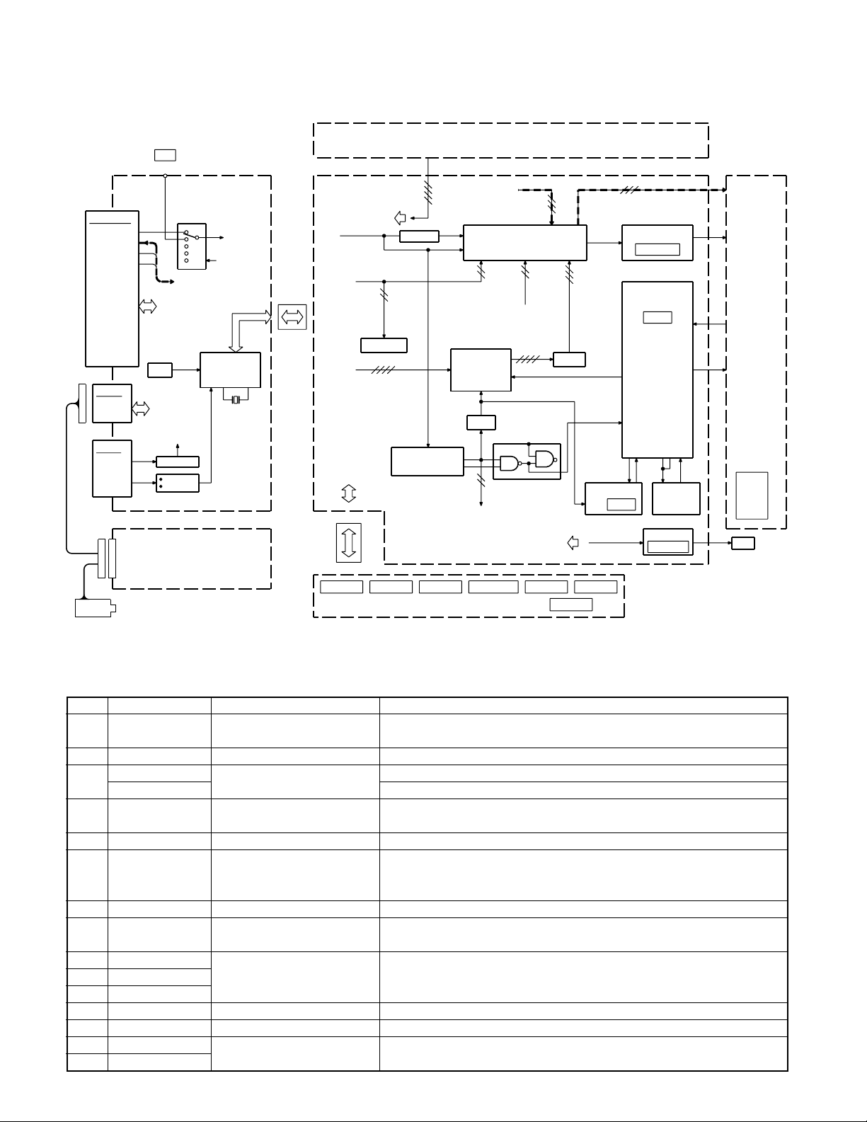
ELECTRIC CIRCUIT MODULE
to
MI-COM
IC302
RST
to
MI-COM
LED. GND
ILL-CONT
IC202
to X35
RST
PARK
B.U. DET
COMP VIDEO
CHROMA
DECODER
IC301
MI-COM
VI1
VI2
VI3
to X35
20MHz
Y/C
BLOCK DIAGRAM
TOUCH PANEL SWITCH ASSY
(X35- ) (A/2)
COMP VIDEO
MI-COM
MI-COM
MI-COM
MI-COM
I2C BUS
OSD RGB
DATA,CLK
EEP ROM
X-DT
Y0
Y-DT
Y0
C. TRAP
IC700
IC400
SYNC
SEPARATION
Y
C
IC500
HD
VD
IC701
OSD
HSY
BUFF
HD,V
to IC701
from X14
CHROMA DECODER
RGBI
VSY
IC402,403
IC401
HD,V
from IC400
RGBI
MI-COM
IC501
NR
NG
NB
OSD
BUFF
V COM
IC202
FLIP FLOP
CLK
BRT
RGB
IC301,Q302,303
VCOM DRIVER
+13V/-16V
IC200
TIMING
CONTROL IC
VSY
SYNI
CVOP
VIN
+5.0V
Q600-604
+5.0V
OSCO
OSCI
PLL
+5.0
INVERTER
BL +9.0V
Q200,
IC201
RGB
LCD ASSY
VCOM
6.5INCH TFT
LCD
SPOI
MOD1
MOD2
VRSP
SCLS
CLDS
PIOCT
+13.0V
+5.3V
-9.6V
-11.1V
CFL
SOURCE NAVI DISP
(X35- ) (B/2)
VOL DOWN
VOL UP
POWER
RESET
COMPONENTS DESCRIPTION
●VIDEO CONTROL UNIT (X14-9172-70)
Ref.No.
Component Name Application/Function Operation/Condition/Compatibility
IC2 FA7611CE AVR control IC
IC202 BA7649F Video SW Video in for the adjustment and NAVI signal selector
70F3033AGC1Q6
IC301
S-80842CNNB
IC302
S-80837CNNB For Mask MI-COM. : When BU5V line voltage is less than 3.7V, IC outputs Lo.
System MI-COM.
Reset IC
IC304 TA78DL05F AVR IC (BU5V AVR) While BACKUP is applied, AVR outputs +5V.
Q1 2SC4081 BU detection SW When momentary power down has detected, a base goes Lo, and Q1 is turned
Q2 DTA124EUA Parking detection SW When the PRK line goes Lo, Q2 is turned on.
Q3 DTB123YK SW5V SW
Q4 DTA124EUA
Q5 2SC4081 Flyback SW
Q6 DTC124EUA
Q7 2SC4979 Flyback driver For the flyback trans driver
Q8 2SA2013 DC/DC chopper For LED9V power line and BL8.5V power line driver
Q9 2SC4081
Q10 2SA1576A
DC/DC chopper driver For Q8 driver
Voltage control of the flyback circuit and the step down type switching
regulator for LED9V and BL8.5V power lines
Flash MI-COM.
Mask MI-COM.
For Flash MI-COM. : When BU5V line voltage is less than 4.2V, IC outputs Lo.
While BACKUP is applied, a base goes Hi, and Q1 is turned on.
off.
When a base goes Lo, Q3 is turned on, and BU5V power line is supplied to
the microprocessor peripheral circuits and the inter nal power supply.
When Q6's base goes Hi, Q4 and Q5 are turned on, and the fly back circuit is
working.
2

SVT-M700
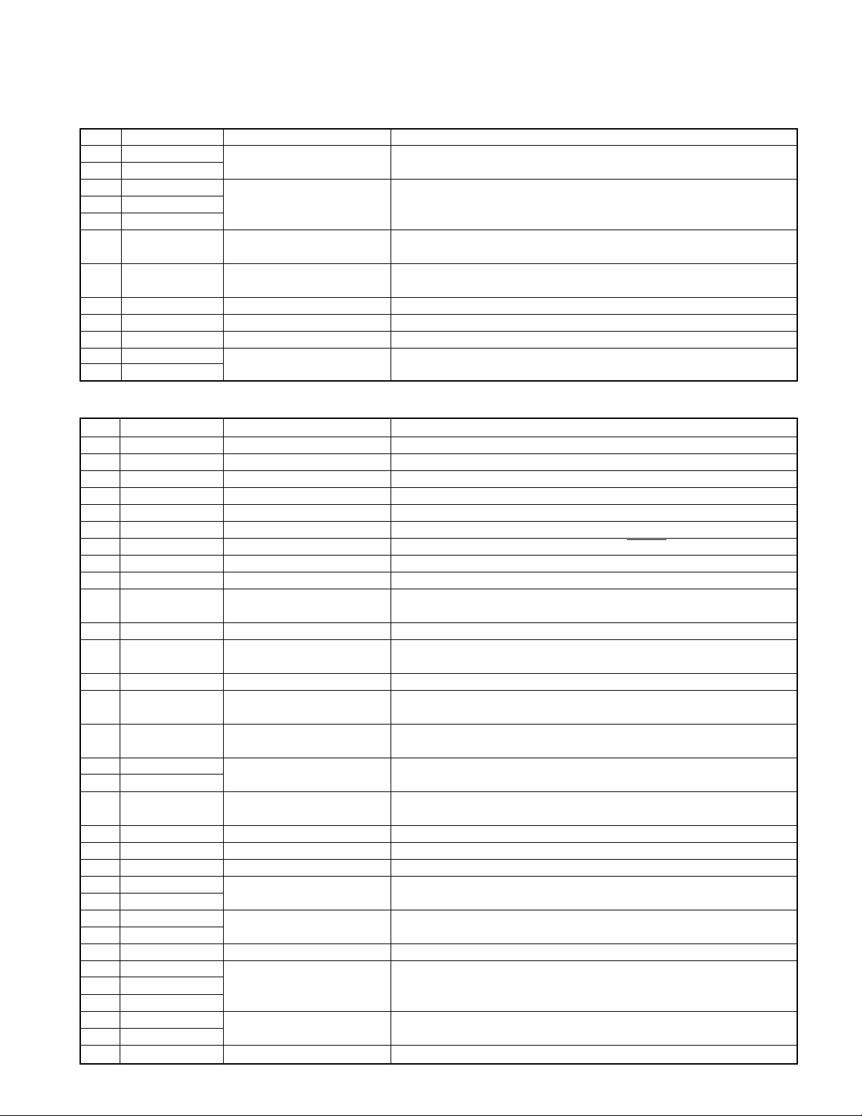
COMPONENTS DESCRIPTION
Ref.No.
Component Name Application/Function Operation/Condition/Compatibility
Q11 2SA1428
Q12 2SC2412K
Q201 2SC4081
Q202 2SA1576A Video buffer Video signal amplifier and buffer
Q203 2SC4081
Q301 DTC144EUA Reset SW
Q302 DTA124EUA Panel reset SW
Q309 2SC4081 VOL DOWN detection SW When VOL DOWN SW is pressed, Q309 is turned off.
Q310 DTC124EUA Buzzer SW
Q311 DTC124EUA Dimmer detection SW When Dimmer control signal from the vehcle is applied, Q311 is turned on.
Q312 2SA1576A
Q313 DTC124EUA and Q313 are turned on.
●VIDEO UNIT(X35-4272-70)
Ref.No.
Component Name Application/Function Operation/Condition/Compatibility
IC200 LZ9GJ24 Timing controller IC LCD module control
IC201 NJM2107F Op. amplifier LPF for PLL control (VT voltage control)
IC202 TC74AC74FT D flip-flop The delay of the vertical start position of the screen
IC301 NJM4580V Op. amplifier COM amplifier and buffer driver
IC400 NJW1303V
IC401 TC7W00FU NAND NAND of HD signal and VD signal, the burst gate pulse polarity inverted
IC402 TC7W34FU Buffer Buffer of HD signal, the burst gate pulse and HD+VD
IC403 TC7W34FU Buffer Buffer of HD signal and VD signal
IC500 MB90096-234 OSD control IC On screen display controller
IC501 TC74HC07AFE OSD signal buffer
IC700 BR24C01AF-W EEPROM The memory of the touch panel adjustment data and the chroma data
IC701 AN2546FH-A Video signal processor IC
IC703 NJU7200U30 3.0V AVR For the video signal processor IC
Q10 DTC143ZUA Touch panel Y0 SW
Q11 DTC143ZUA Touch panel X0 SW
Q12 DTC143ZUA
Q13 DTA143ZUA power line is applied to the touch panel assembly.
Q14 DTA143ZUA Touch panel X1 SW
Q200 2SC2411K VCO For PLL oscillation
Q300 2SC4081 Ripple filter For the video signal processor IC and V COM amplifier circuit
Q301 2SC4081 7.5V AVR +7.5V AVR for the video signal processor IC
Q302 2SA1577
Q303 2SC4097
Q401 2SC4081
Q403 2SA1576A
Q500 2SC4081 I buffer OSD half brightness control
Q600 DTC124EUA
Q601 DTA143XUA Inverter SW
Q602 2SC2873
Q603 2SD1803
Q604 2SD1803
Q700 2SC4081 Y buffer Brightness signal buffer
Voltage limiter Power supply voltage limiter and Ripple filter
When the panel reset SW is pressed, Q301 is turned on, and the system MICOM. is reset.
When the panel reset SW is pressed, Q302 is turned on, and the reset signal
is output to STC-700.
LED SW
Synchronising pulse separation IC
Touch panel Y1 SW
COM buffer V COM signal driver
C.SYNC buffer Video signal or the navigation C.SYNC signal buffer
Inverter driver For the back light inverter trans driver
When LED brightness control signal (PWM) from the vehcle is applied, Q312
HD signal and VD signal pulse separation and the burst gate pulse generation
Buffer of R signal, G signal, B signal, I signal and the inverted burst gate pulse
signal
The video signal processing of LCD drive, the chroma decoder and
γ compensator
When Y axis input mode is selected, Q10 is turned on.
When X axis input mode is selected, Q10 is turned off.
When X axis input mode is selected, Q11 is turned on.
When Y axis input mode is selected, Q11 is turned off.
When Y axis input mode is selected, Q12 and Q13 are turned on, and SW5V
When the panel touch is detected or the X axis input mode is selected, Q14 is
turned on, and SW5V power line is applied to the touch panel assembly.
When Q600's base goes Hi, Q601 and Q602 are turned on, and the inverter
circuit is working.
3

SVT-M700
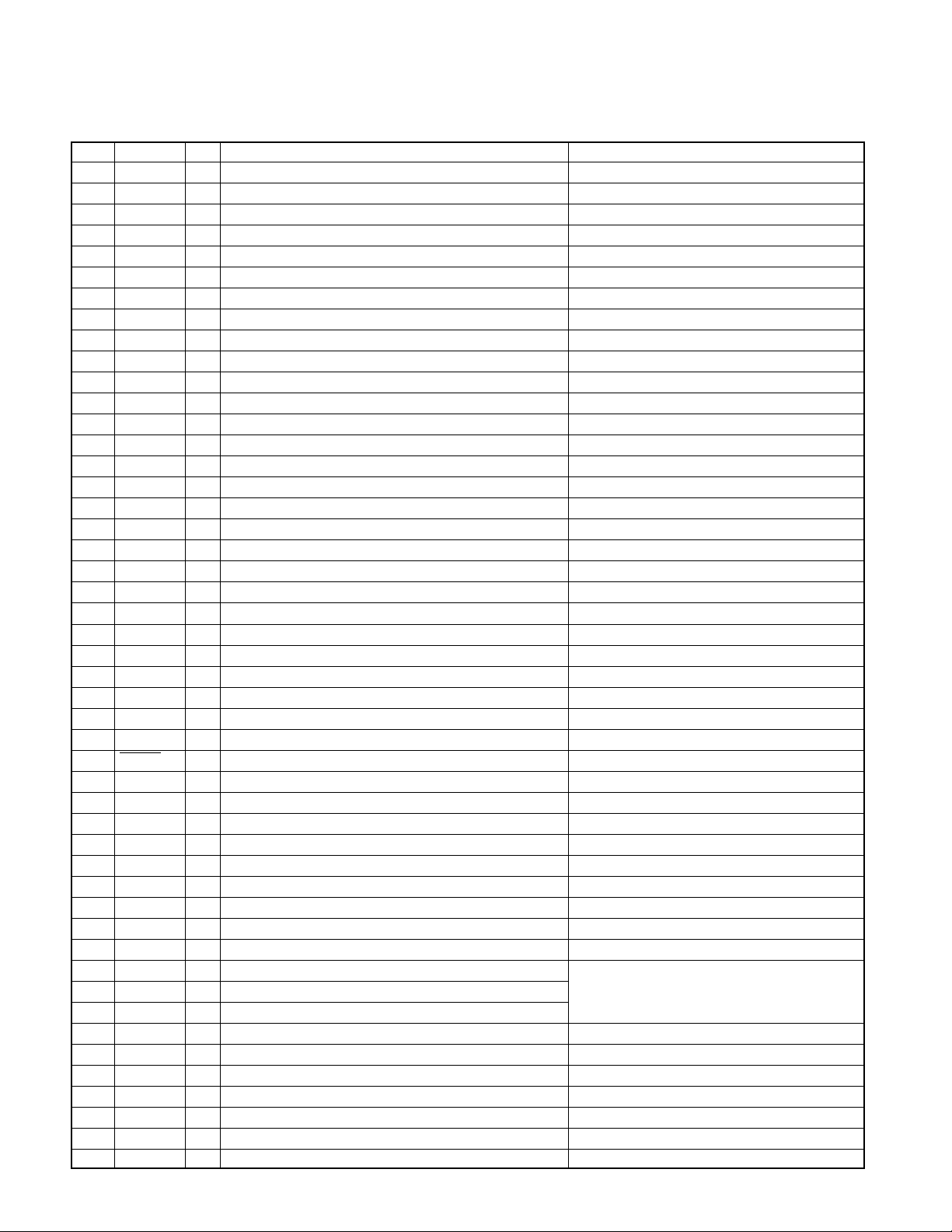
MICROCOMPUTER’S TERMINAL DESCRIPTION
●IC301 (VIDEO CONTROL UNIT : X14-9172-70)
Pin No.
44, 45 VO 1, 2 O Video out SW control Not used (N.C.)
46, 47 AO 1, 2 O Audio out SW control Not used (N.C.)
48, 49 AB 1, 2 O Speaker out SW control Not used (N.C.)
Pin Name I/O Description Processing Operation
1 M DATAC O Data output to STC-700
2 M CLK I Data clock input from STC-700
3 OSD CS O OSD chip select output
4 OSD DO O OSD data output
5 OSD CK O OSD clock output
6 EVDD - Positive power supply connection terminal Connected to BU5V lines.
7 EVSS - Ground connection terminal Connected to GND lines.
8 OSD RST O OSD reset output Lo : Reset
9 OSD TRE I Communication permission input from the OSD IC Hi : Busy
10 VSYNC O V SYNC signal input Not used (N.C.)
11 SYNC SW O V SYNC signal input selector output Not used (N.C.)
12 REMO I Remote control signal input
13 SDA I/O I2C BUS data input/output
14 SCL I/O I2C BUS clock output
15 DIMMER O Dimmer output PWM output, Duty variable, Approximately 150Hz
16 HSY I H SYNC signal input for the OSD IC control
17 BEEP O BEEP output
18 IC/VPP - Flash data writing terminal Not used(connected to GND lines)
19 P100 O Not used (N.C.)
20 PARK SW I Parking detection input Hi : Parking ON, Lo : Parking OFF
21 EX MP O Panel mechanism slide motor output + Not used (N.C.)
22 EX MN O Panel mechanism slide motor output - Not used (N.C.)
23 RI MP O Panel mechanism tilt motor output + Not used (N.C.)
24 RI MN O Panel mechanism tilt motor output - Not used (N.C.)
25 PON O PON output Lo : Power ON, Hi : Power OFF
26 MEC PON O Panel mechanism connection detection input Not used (N.C.)
27 MOT SW O Motor applied voltage switching terminal Not used (N.C.)
28-30 P111-113 O Not used (N.C.)
31 RESET I Reset input terminal Lo : Reset
32 XT1 I Sub clock resonator connection terminal Not used (pull down to GND lines)
33 XT2 - Sub clock resonator connection terminal Not used (N.C.)
34 REGC 35 X2 - Main clock resonator connection terminal
36 X1 I Main clock resonator connection terminal
37 VSS - Ground connection terminal Connected to GND lines.
38 VDD - Positive power supply connection terminal Connected to BU5V lines.
39 CLKOUT O Internal clock out terminal Not used (N.C.)
40 AB MUTE O Audio muting control output to STC-700 Hi : Muting ON, Lo : Muting OFF
41 VI 1 O Video in SW control 1 NAVI : (VI 1, VI 2, VI 3) = (Lo, Lo, Lo)
42 VI 2 O Video in SW control 2 VIN : (VI 1, VI 2, VI 3) = (Lo, Hi, Lo)
43 VI 3 O Video in SW control 3 MUTE : (VI 1, VI 2, VI 3) = (Lo or Hi, Lo or Hi, Hi)
50 AO MUTE O Audio out muting control Not used (N.C.)
51 LED R O LED R indicator output Not used (N.C.)
52 LED G O LED G indicator output Not used (N.C.)
53 LED B O LED B indicator output Not used (N.C.)
Capacitor connection terminal for regulator inside microprocessor
4
 Loading...