

Page 1
STEREO INTEGRATED AMPLIFIER/TUNER
stereo integrated amplifier/tuner
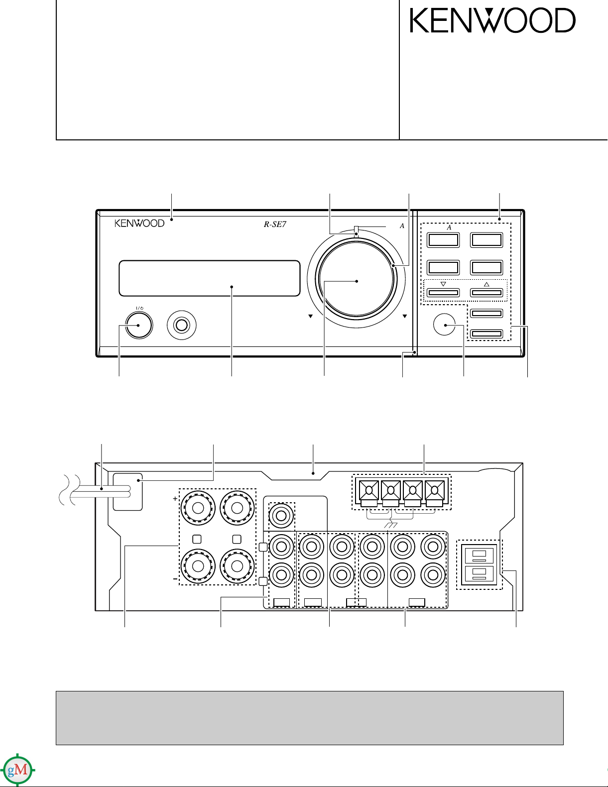
on/standby
phones
down up
volume
control
pure
input selector
N.B.
pure
enter
band
auto/mono
turning
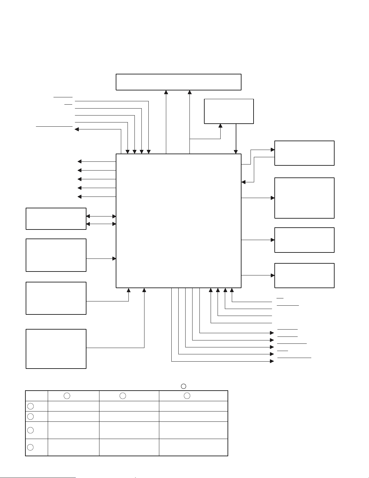
SPEAKER
(6 – 16 Ω)
R
L
SUB
WOOFER
PRE OUT
FM75Ω
FM300Ω GND
AM
ANTENA
SYSTEM
CONTROL
R
L
IN IN
CD AUX
REC OUT
PLAY OUT
REC OUT
PLAY OUT
TAPE
MD
R-SE7/SE-7(G)
SERVICE MANUAL
(HM-701)
©1997-10/B51-5373-00 (K/K) 3191
Knob
(K29-6744-04)
AC power cord *
(E30-)
Panel *
(A60-)
Front glass
(B10-2373-03)
Power cord bushing
(J42-0083-05)
Indicator
(B12-0322-04)
Knob
(K29-6358-04)
Metallic cabinet *
(A01-)
Escutcheon
(B07-2367-03)
Escutcheon
(B07-2363-04)
Lock terminal board
(E20-0476-05)
Panel *
(A60-)
Indicator
(B12-0320-04)
Knob
(K29-6750-03)
Lock terminal board *
(E70-)
PRECAUTIONS FOR REPAIR
• For the SERIAL TEST CODE LIST of the circuit description, see Service manual (B51-5210-00) of R-SA7.
Phono jack
(E63-1014-05)
• No connection of ground line if disassemble the unit.
• Please connection the ground line on rear panel, PCBs, Chassis and some others.
Phono jack
(E63-0046-15)
Phono jack
(E63-0047-15)
Rectangular receptacle
(E08-0312-05)
* Refer to parts list on page 25.
Page 2
DISPLAY
SLEEPTAPE
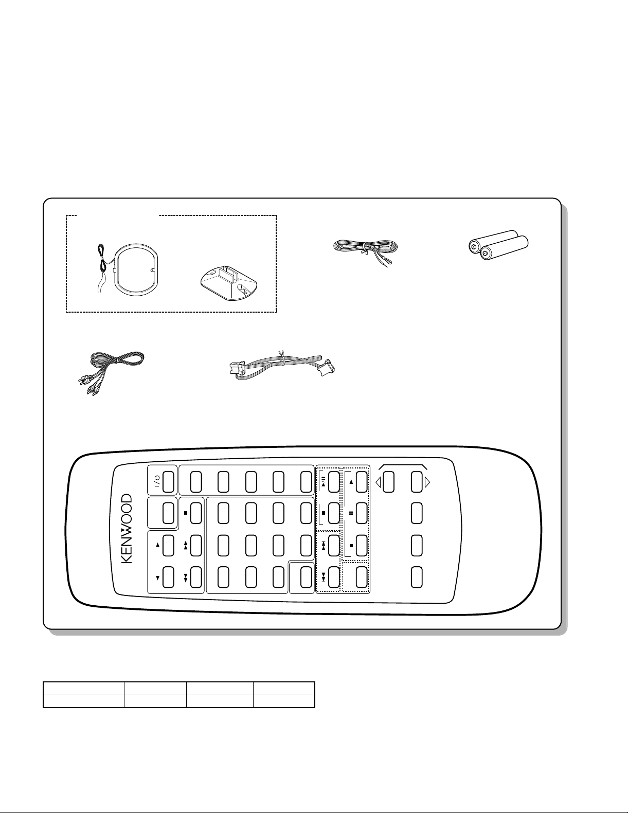
REMOTE CONTROL UNIT
RC-SE9
1 2 3 RANDOM
4 5 6 CLEAR
7 8 9 P.MODE
O.T.E. 0 +10 EDIT
TUNER
BAND
INPUT N.B. MUTE
VOLUME
CONTROL
MD
CDP.CALL
R-SE7/SE-7(G)
CONTENTS / ACCESSORIES
Contents
CONTENTS / ACCESSORIES .................................. 2
CIRCUIT DESCRIPTION............................................3
ADJUSTMENT............................................................8
PC BOARD .............................................................. 10
Accessories
SCHEMATIC DIAGRAM.......................................... 13
EXPLODED VIEW ....................................................24
PARTS LIST..............................................................25
SPECIFICATIONS ......................................Back cover
AM loop antenna (1)
(T90-0820-05)
Audio cords (2)
(E30-0615-05)
Remote control unit (1)
(A70-1154-05) : KM
(A70-1155-05) : TE
AM loop antenna stand (1)
(J19-3645-05)
System control cord (1)
(E30-2628-05)
FM indoor antenna (1)
(T90-0182-15) : KM
(T90-0806-05) : ET
Batteries (R6/AA) (2)
Battery cover (A09-0374-08)
System configuration
SYSTEM NAME AMP/TUNER CD PLAYER SPEAKER
HM-701 R-SE7 DP-SE7 LS-SE7
2
Page 3
R-SE7/SE-7(G)
Channel
BAND
E TYPE
Channel
BAND
E TYPE
01chFM87.50MHz
11chFM90.00MHz
02chFM97.50MHz
12chFM98.00MHz
03ch
FM
108.00MHZ
13chFM98.50MHz
04chAM630kHz
14ch
FM
106.00MHz
05chAM990kHz
15chAM531kHz
06chAM1440kHz
16chAM990kHz
07chFM87.50MHz
17chAM1602kHz
08chFM87.50MHz
18chFM87.50MHz
09chFM87.50MHz
19chFM87.50MHz
10chFM89.10MHz
20chFM87.50MHz
CIRCUIT DESCRIPTION
1. INITIAL STATE
(1) AMP-related block
EPOWER OFF
ESELECTOR SOURCE TUNER
EDISPLAY SELECTOR
EN.B. CIRCUIT OFF
EA CLASS VOLUME VALUE 1.40 STEP
EAB CLASS VOLUME VALUE 7 STEP
EPURE MODE NORMAL (AB CLASS)
EAUTO POWER SAVE OFF
EMULTI CONTROL MODE INPUT SEL.(R-SE9 only)
(2) TUNER-related block
EBAND FM
EFREQUENCY Lower-limit value of
FM 87.5 MHz
AM 531 kHz
EAUTO/MANUAL AUTO
EP.CH MEMORY Last frequency
ELast P.CH 01ch
E
RDS DATA TABLE MEMORY
(3) TIMER-rated block
ECLOCK STOP (AM12:00)
EPROGRAM WORKING MODE OFF
CONTENTS OF PROGR
EO.T.T WORKING MODE OFF
OTT ON TIME AM 7:00
(4) TEST PRESET FREQUENCY
ƒThe initial setting is performed in a following event :
1. When backup memory data is destroyed when reset is
applied to the microprocessor.
2. When the power cord is plugged in to the AC wall outlet
while pressing the on/standby key.
receiving frequency.
NO DATA
. ON=AM 12:00
OFF=AM 12:00
PLAY MODE=PLAY
SELECTOR=TUNER(1ch)
REC MODE OFF
2. BACKUP
This function holds the current state of the unit even if the
AC power of the receiver is turned OFF.
(1) Operation outline
The backup state set command signal (CE) of a microcom-
puter is set low when the AC power is turned OFF. The
microcomputer detects the signal and enters the stop state.
The microcomputer is reset when the AC power is turned
ON. The data for backup state confirmation is checked by
reset processing.
The microcomputer is initialized when the data was
destroyed. If it is not destroyed, the microcomputer is started
in the backup state.
EThe data for backup state confirmation is written in a RAM
area.
E The microcomputer is set to the STOP mode so as to
save the power consumption.
EA backup state set command signal is detected by a timer
interrupt of 1 msec.
EThe backup guarantee period is set in a circuit.
(2) Backup state setting
EThe data (A596, 5A69H) for backup state confirmation is
written in a RAM area.
(3) Contents of backup data to be held
[[[ AMP [[[
EPOWER ON/OFF
EDISPLAY MODE
ESELECTOR SOURCE
EN.B. CIRCUIT MODE
EA CLASS VOLUME VALUE
EAB CLASS VOLUME VALUE
EPURE A MODE
[[[ TUNER [[[
ELAST BAND
EPRESET CHANNEL/RECEIVING STATION FRE-
QUENCY/PI/TA/PTY/PS
E LAST RECEIVING STATION FREQUENCY AND PRE-
SET CHANNEL (AM/FM)
EPRESET MEMORY data (1ch~40ch)
EAUTO/MANUAL
[[[ CLOCK/TIMER [[[
ELAST CLOCK DATA
E PROGRAMMED CONTENTS/PROGRAM TIMER WOR-
KING MODE ON/OFF
EO.T.T. SETTING TIME/O.T.T. WORKING MODE
ON/OFF
3
Page 4
R-SE7/SE-7(G)
CIRCUIT DESCRIPTION
3. DESTINATION LIST OF TUNER
3-1 Destination List of Tuner
Desti-
nation
K1
E1
E3
(RDS)
M
Receive
BAND frequency
range frequency
87.5MHz~
FM
108.0MHz
530kHz~
AM
1700kHz
87.5MHz~
FM
108.0MHz
531kHz~
AM
1602kHz
87.5MHz~
FM
108.0MHz
531kHz~
AM
1602kHz
K2 or E1 is changed the setting "DSW1".
(DSW1=1 : K2, 0 = E1)
0 : NO DIODE 1 : DIODE X : SWITCHING TRANSISTOR
Channel
space
100kHz +10.7MHz 25kHz
10kHz +450kHz 10kHz
50kHz +10.7MHz 25kHz
9kHz +450kHz 9kHz
50kHz +10.7MHz 25kHz
9kHz +450kHz 9kHz
1F reference DSW1 DSW2
PLL
DIODE SW
D518 D519
1 1
0 1
1 0
X 1
4. TEST MODE
4-1. Initializing
The system is initialized when the power is turned on while
pressing the on/standby key.
(1) Contents of operation
EAll the functions are initialized.
4-2. AMP test mode using main unit's keys
4-2-1. Entering the AMP test mode
ETurn on the power while pressing the BAND key.
4-2-2. Canceling the AMP test mode
EBy turning off the power, the system is initialized and the
test mode is canceled.
4-2-3. Contents of AMP test mode
(1) Automatic on/standby ON
EThe POWER ON state is entered whenever the power is
turned on while pressing the BAND key. All functions are
then initialized and activated in the all-lighting mode.
ESub-clock oscillation diagnosis function
The oscillation diagnosis (existence of oscillation and
measurement of period) of a sub-clock is performed
before the test mode is entered. If the diagnosis result is
OK, the system enters the test mode.
If the diagnosis result is NG, the oscillation of the sub-
clock is diagnosed again. If the result is OK, the system
enters the test mode. If the diagnosis result is continu-
ously NG five times, the system stops with ERR 1 and
ERR 2 displayed.
(2) All-lighting mode
EAll the fluorescent display indicators and LED lamps light
when the power is turned on while pressing the BAND
key.
E After that, the all-lighting mode is canceled when any
main unit's key is pressed. The normal display obtained
when the selector is set to TUNER then appears.
(3) Others
EThe AMP test mode is not terminated even if the selector
is set to positions other than TUNER.
EIn the AMP test mode, the muting during mode selection
is not controlled. However, the operation during the
power-on sequence is the same as the normal operation.
EThe SP protection operation is also the same as the nor-
mal operation.
E In the AMP test mode using main unit's keys, the keys
below provide a special operation according to the position where the selector is set. The main unit's keys
except described below and the rotary encoder provide
the normal operation.
(4) When selector is set to TUNER
Key Operation
PURE A key Increments the P.CALL every time this
key is pressed.
N.B. key Decrement the P.CALL every time this
key is pressed.
ENTER key Selects the display cyclically in the order
below every time this key is pressed.
@ Write data in the unused area of E2PROM, then read the
written data. If the read data is the same as the written
data, "RAM OK" is displayed in the fluorescent display
indicator. If the former is different from the latter, "RAM
NG" is displayed.
A Set the TUNER ATT to OFF and display the S level in
hexadecimal when the ENTER key is pressed. ("ATT
OFF **" is displayed in the fluorescent display indicator.)
B Set the TUNER ATT to ON and display the S level in
hexadecimal when the ENTER key is pressed. ("ATT ON
**" is displayed in the fluorescent display indicator.)
* The special display using the ENTER key is continued until
the next operation is carried out. (**: S LEVEL)
When keys other than ENTER are pressed in items @to B
above, the TUNER ATT is set to OFF and the normal display
appears. The operation corresponding to the key that has
been pressed is performed in this case.
(5) When selector is set to positions other than TUNER
[ENTER key] Every time this key is pressed, master VOL-
UME level is selected cyclically.
INITIALIZE level
Value of Master
VOLUME
MAX 86 16.00
MID 40 8.00
MIN 1 0.20
INITIALIZE 7 1.40
Press the ENTER key.
ìî MAX î MID î MIN ì
Press the PURE A key,
then press the ENTER key.
4
Page 5
R-SE7/SE-7(G)
CIRCUIT DESCRIPTION
[ AUTO key ] Selects the MUTE operation and equalizer
cyclically in the order below for operation display every time
this key is pressed.
-- -> MUTE operation -> Minimum -> Maximum ->
ƒ In the operation for except the AUTO key, become pre-
condition equlizer .
ƒPre condition : The equlizer becomes the condition to be
pushed the AUTO key before
(include N.B. circuit).
(6) SERIAL TEST CODE LIST
Refer to Service manual (B51-5210-00) of R-SA7 on
page 7.
[ BAND key ] Every time this key is pressed, all the displays
go off and the normal display is selected cyclically.
ƒPre-condition
--
4-3. RDS test mode using main unit's keys
4-3-1. Entering the RDS test mode
ETurn on the power while pressing the TUNING UP key.
4-3-2. Canceling the RDS test mode
EBy turning off the power, the system is initialized and the
test mode is canceled.
4-3-3. Contents of RDS test mode
EThe POWER ON state is entered whenever the power is
turned on while pressing the TUNING UP key. All the
functions are then initialized.
E In the RDS test mode using main unit's keys, the keys
below provides a special operation according to the posi-
tion where the selector is set. The main unit's keys
except described below and the rotary encoder provide
the normal operation.
Key Operation
CLASS A key Performs the same operation as for
remote control key "DISPLAY" every time
this key is pressed.
INPUT SEL. key Performs the same operation as for
remote control key "PTY" every time this
key is pressed.
N.B. key Performs the same operation as for
remote control key "TA" every time this
key is pressed.
ENTER key Selects the display cyclically in the order
below every time this key is pressed.
B Set the TUNER ATT to ON and display the S level in
hexadecimal when the ENTER key is pressed. ("ATT ON
**" is displayed in the fluorescent display indicator.)
* The special display using the ENTER key is continued until
the next operation is carried out. (**: S LEVEL)
When keys other than ENTER are pressed in items @to B
above, the TUNER ATT is set to OFF and the normal display
appears. The operation corresponding to the key that has
been pressed is performed in this case.
4-4. SERIAL TEST MODE
(1) Setting the serial test mode
The unit is put into the serial test mode when a serial code
"TEST ON" is input during the POWER-ON sequence.
In the 16-bit serial test mode, serial code C27FH is input.
E In the serial test mode, all remote control keys and ordi-
nary serial codes are disabled. Only the panel keys per-
form the same operation as usually.
(2) Canceling the serial test mode
EThe serial test mode is canceled to return to the ordinary
mode by inputting a "TEST OFF" code (C27 EH). After
the ordinary mode was returned, the serial mode is
returned to the state before the test mode is entered.
The backup operation is not initialized.
EThe serial test mode is also canceled when the AC power
is turned OFF.
(3) Cautions
EThe serial test code is prescribed as a 16-bit code only.
EThe operations below are inhibited in the serial test mode.
The operations mentioned above cannot be guaranteed
when they are performed in the serial test mode.
E An identical code is output when the serial test mode
code is input.
@Write data in the unused area of EEPROM, then read the
written data. If the read data is the same as the written
data, "RAM OK" is displayed in the fluorescent display
indicator. If the former is different from the latter, "RAM
NG" is displayed.
A Set the TUNER ATT to OFF and display the S level in
hexadecimal when the ENTER key is pressed. ("ATT
OFF **" is displayed in the fluorescent display indicator.)
5
Page 6
FL DISPLAY (FIP9GM6R)
RESET
CE
REMOCON
LEVEL IN
CLASS A LED
BIAS MID
BIAS HI
LOW RELAY
HI RELAY
SPEAKER RELAY
(X09) J5
(X14) IC2
(X14) S2
DATA
BUSY
ENC-C
ENC-D
(X14) ED1
(X05) IC2
(X09) IC1
(X14) IC3
u-COM
uPD78045FGF057
9
16
4
1
3
3
1
3
2
2
PLL IC
(LC72131)
KEY MATRIX
SELECTOR ANALOG
SW CONTROL IC
(NJU7313AM)
E2PROM IC
(X24C04)
MULTI CONTROL
ENCODER
(R-SE9 only)
(X14) S1
ENC-A
ENC-B
2
VOLUME ROTARY
ENCODER
(X14) IC4
SIGNAL LEVEL
RDS CLOCK
RDS DATA
3
RDS
(X09) IC3
2
ELECTRIC VOLUME
IC (M62420)
SD
STEREO
HEAD PHONES
PROTECTION
A MUTE
T MUTE
H. P. MUTE
ATT
A CLASS ON
✽
SERIAL
R-SE7/SE-7(G)
CIRCUIT DESCRIPTION
5. Microprocessor : uPD78045FGF057 (X14 : IC1)
5-1 Microprocessor periphery block diagram
Key matrix
64
KS0 DSW0 DSW1 (D158) DSW2 (D159)
63
KS1 POWER AUTO / MONO BAND
62
KS2 N. B. CIRCUIT
61
KS3 pure A ENTER
6
60
KR0
No. of : u-COM port No.
59
KR1
(R-SE7) INPUT SEL.
(R-SE9) MODE
(R-SE7) TUNING UP
(R-SE9) No. use
(R-SE7) TUNING DOWN
(R-SE9) No use
58
KR2
Page 7
R-SE7/SE-7(G)
CIRCUIT DESCRIPTION
5-2 Pin description
Pin No. Name I/O Description Active
1~7 7G~1G O FL grid 7~1 —
8 VDD — Micro processor power supply (+5V) —
9 E2PROM SCL O E2PROM control clock —
10 E2PROM SDA I/O E2PROM control data —
11 ENC C — Multi control encoder input A —
12 ENC D — Multi control encoder input B —
13 A CLASS ON O Power ON/OFF control signal H : OFF L : ON
14 SEL STB O Selector IC strobe —
15 SEL/PLL CLK O SEL/PLL IC control clock —
16 SEL/PLL DATA O SEL/PLL IC control data —
17 RESET I Microprocessor reset L : RESET ON
18 CE I AC OFF(MAIN POWER) detection Signal L : AC OFF
19 PLL DO O IF count data —
20 AVSS — A/D power SUPPLY (GND) —
21 PLL CE O PLL chip enable control L : CE
22 T MUTE O Tuner mute signal L : MUTE ON
23 STEREO I Stereo signal detection L : STEREO ON
24 SD I Synchronized signal detection —
25 VOL SCL O Electric volume IC control clock —
26 VOL SDA O Electric volume IC control data —
27 LEVEL IN I Volume level input —
★ 28 S.LEVEL(RDS) I Signal level —
29 A VDD — A/D power supply (+5V) —
30 A VREF — A/D reference voltage(+5V) —
31, 32 OSC — 32kHz oscillator —
33 Vss — Microprocessor power supply (GND) —
34, 35 OSC — 4.19MHz oscillator —
36 S.DATA I/O 16bit system data —
37 S.BUSY I/O 16 bit system busy H : BUSY L : READY
38 H.P. MUTE O Head phones mute signal L : ON
39 ATT O CLASS A control signal H : A CLASS L : AB CLASS
40 A MUTE O Audio mute signal L : ON
41 HIGH RELAY O AMP high relay control H : ON L : OFF
42 LOW RELAY O AMP low relay control H : ON L : OFF
43 SP RELAY O Speaker relay control H : ON L : OFF
★ 44 CLK(RDS) I RDS clock —
★ 45 DATA(RDS) I RDS data —
46 PROTECTION I Protection detection H : ON L : OFF
47 REMOCON I Remote control input —
48 IC — — —
49 CLASS A LED O CLASS A LED H : OFF L : ON
50 BIAS MID O Bias control signal MID —
51 BIAS HI O Bias control signal HI —
52 VDD — Microprocessor power supply (+5V) —
53 ENCA I Volume encoder in put A —
54 ENC B I Volume encoder input B —
55 HEAD PHONE I Head phones signal detection H : ON L : OFF
56, 57 NC O — —
58~60 KR2~KR0 I KEY return 2~0 H : KEY ON
61~64 SEG16~13/KS3~0 O FL Segment 6~13 /key scan 3~0 H : ON
65~70 P12 SEG12~SEG7 O FL Segment 12~7 H : ON
71 V load — FL drive power supply (-30V) —
72~77 P6 SEG6~SEG1 O FL Segment 6~1 H : ON
78 NC O — —
79, 80 9G, 8G O FL grid 9, 8 —
★ E/T type only, other types unused.
The RDS PTY AF search always corresponds to a span search of 100kHz. Therefore, a span search of 50 KHz
cannot be performed.
7
Page 8
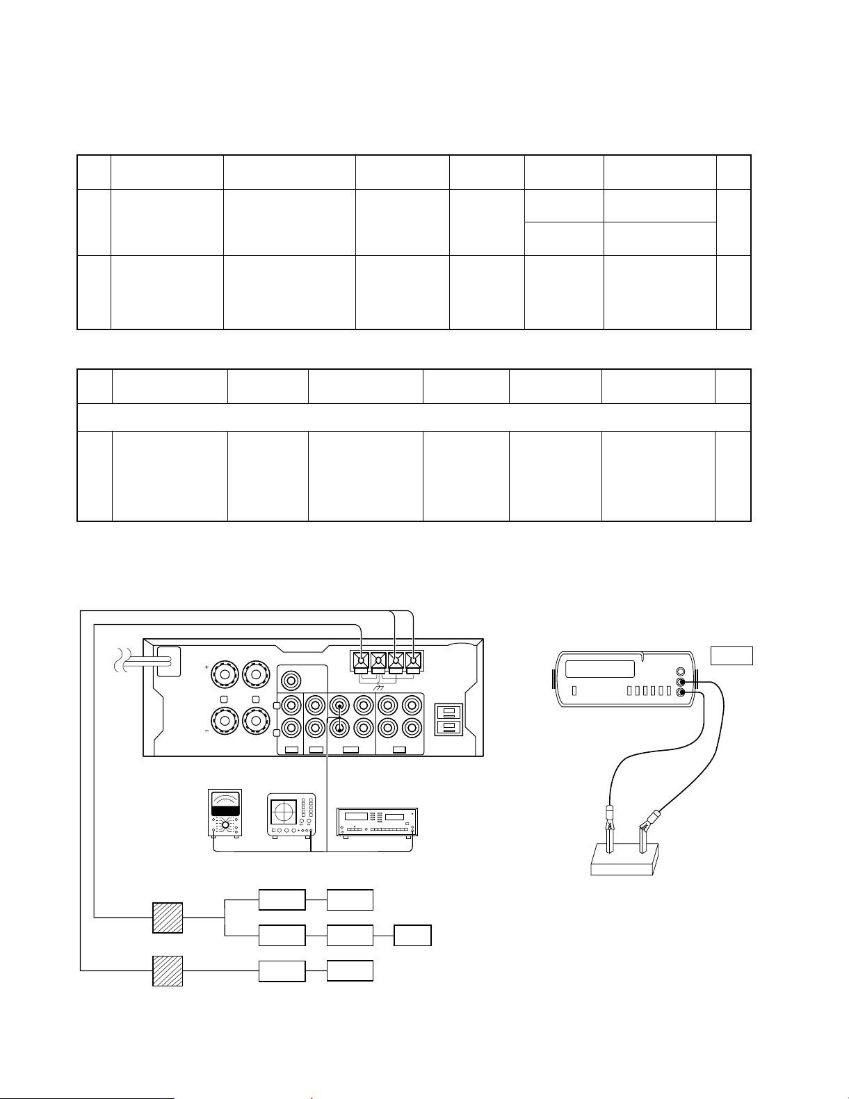
R-SE7/SE-7(G)
NO.
ITEM
INPUT
SETTINGS
OUTPUT
SETTINGS
TUNER
SETTINGS
ALIGNMENT
POINTS
ALIGN FOR
FIG.
1
DISCRIMINATOR
(A)
98.0kHz
1kHz, ±75kHz dev.
60dBµ(ANT input)
Connect a DC
voltmeter
between
Pin 1 and Pin 2
of CN 2.
MONO
98.0MHz
L 31
0V
(a)
L 32
Minimum distortion.
2
DISTORTION
(STEREO)
(C)
98.0MHZ
1kHz, ±68.25kHz dev.
Pilot: ±6.75kHz dev.
60dBµ(ANT input)
(B)
AUTO
98.0MHz
IFT (A1)
Minimum distortion.
(a)
NO.
ITEM
INPUT
SETTINGS
OUTPUT
SETTINGS
AMP
SETTINGS
ALIGNMENT
POINTS
ALIGN FOR
FIG.
POWER: ON SELECTOR : AUX
1
B CLASS
IDLE CURRENT
Connect a DC
voltmeter across
CN1(L)
CN2(R)
(X09, A/7)
PURE A : OFF
Volume : 0
VR1(L)
VR2(R)
(X09, A/7)
20mV
(b)
SPEAKER
(6 – 16 Ω)
R
L
SUB
WOOFER
PRE OUT
FM75Ω
FM300Ω GND
AM
ANTENA
SYSTEM
CONTROL
R
L
IN IN
CD AUX
REC OUT
PLAY OUT
REC OUT
PLAY OUT
TAPE
MD
Oscilloscope
Distortion meter
AC voltmeter
Dummy antenna
(A)
(B)
(C)
(D)
AG
AG
FM SG
MPX
AG
FM SG
AM SG
(a) (b)
CN1(L)
CN2(R)
Dc voltmeter
20mV
FM SECTION SELECTION :FM
X05-4622-71 (E/T TYPE)
AUDIO SECTION (X09-469x-xx)
ADJUSTMENT
—
SYSTEM CONNECTIONS
8
Page 9
R-SE7/SE-7(G)
PARTS DESCRIPTIONS
9
Page 10

A C EB D
PC BOARD(Component side view
1
2
3
TUNER UNIT (X05-4600-12) : K
(X05-4600-72) : M
)
4
TUNER UNIT (X05-4622-71) : ET
5
6
7
10
Refer to the schematic diagram for the value of resistors and capacitors.
Page 11

FHJLNGIKMO
PC BOARD(Component side view
1
2
3
)
AUDIO UNIT (X09-4690-11) : K
(X09-4690-21) : M
(X09-4692-71) : ET
4
5
6
7
Refer to the schematic diagram for the value of resistors and capacitors.
11 12
Page 12

A B D F H JC E G I
-B LINE
+B LINE
IC1
IC2
TUNER UNIT (X05-4600-xx)
AM
IFT
OSCRF
:
:
D3,4
: 2SC4116(Y,GR) orQ5
2SC4177(C5,C6)
D4
UZ-5.1BSB
MTZJ5.1(B)or
IC
FM 300Ω
D8
SW
FM/AM
IC
SYSTEM
FM/AM
Q5
FM
D10 MA111
HSS104
2SA1611(M5,M6)
Q3
PLL
D3
:IC4 NJM4565M
D2
D1
Q1
FM IF
AMP
LC72131
LA1832
:
:
IC2
IC1
2SC2714(R.O)
:
:Q1
Q3
:D1,2,8 1SS133 or
2SA1586(Y,GR) or
AM ANT
GND
FM 75
J1
J2
Ω
+12V
+12V
-B
+B
SIGNAL LINE
GND LINE
+5V+5V
+5V +5V+5V
+5V +5V
+5V
+5V +5V+5V
+B
+B+B
+B +B
+B
+B
+B+B+B +B
+B
+12V +12V
+5V
+5V +5V
+5V
+12V +12V
+12V+12V +12V
0V(0.6V)
VT VOLTAGE
LF:LOW FREQUENCY
HF:HIGH FREQUENCY
VT VOLTAGE
4.7V
1.2V
4.1V
1.7V
HF
LF
HF
LF
FREQ.
AM
FM
BAND
0.2V(1.9V)
13.1V
12.9V(0V)
12.1V
0V(10.4V)
2.5V(0V)
ST:4.0V
MONO:0V
5.1V0V0V0V
2.5V
0V
0V
1.0V
1.0V
4.4V
2.5V
5.1V
2.1V
11.2V
1.3V
5.1V
5.1V
5.2V
2.1V
2.1V
2.1V
(3.8V)
(1.3V) 4.0V(0V)
2.1V
(1.0V)(3.0V)
5.2V
3.7V
1000P
C5
22P
C63
1K
R40
C4
0.01
4.7u25
C19
R14 7.5K
1W
+
C25
10u16
R41
180
1K
R20
C52
47P
UNTUNE:4.9V
2.5V
ST:0V
MONO:4.7V
3.2V
0V
4.0V
2.5V
(2.0V)
2.4V
5.2V
(2.1V)
1.8V(2.1V)
1.3V
MONO:2.7V
ST:4.2V
2.5V(0V)
FM:11.0V
TUNE:0V
+12V
R30
1K
1/4W
C3 4P
R46
100K
1
2
3
4
8.2K
R19
C23
1u50
+
X2
456KHz
47K
R13
47K
R7
C21
C22
5600P
C17
1000P
C18
10u16
+
C16
LOWCUT
PILOT
SMETER
OSCBUFF
SW
DET
15K
R47
C13
1000P
+
C14
1u50
C15
22P
47K
R48
3K
R18
+
C12
2.2u50
1u50
C11
+
CF3
10.7MHz
270
R17
L2
R44
100
0.01
C8
10
11
7
8
9
6
45312
12
13
14
15
16
17
18
19
20
22
21
R25
100
L4
1uH
0.01
1000P
47u10
10K
1K
2.2K
1000P
100P
2.2u50
+
1/4W
R26
560
R24
5.6K
R70
C29
R32
1.2K
12K
R33
C32
C31
C35
R28
R29
1K
C34
C33
R31 10K
6
R27
R22
R23
1K
1K
C38
R21
1K
470P
7.2MHz
X1
C37
22P
C36
27P
5
4
3
+
100u16
C30
+
24
23
22
20
19
17
16
18
21
141513
1
OSC
FMSDADJ
2
AMMIX
FMIF
AFC
3
REG
AMRF
5
AMIF
AM
6
SD
GND
AMAGC
DETOUT
8
STEREO
MPXIN
9
VCC
FMDET
MPXVCO
7
4
R
IFCOUNT
DET
L
FM/AM
PHASE
12
11
10
+
C9 10u16
C10 0.047
AMIFOUT
C20
0.1
ON
RESET
12bits PROGRAMABLE
DIVIDER
SWALLOW COUNTER
1/16,1/17 4bits
UNIVERSAL COUNTER
2
DATA SHIFT REGISTER LATCHC B I/F
DETECTOR
UNLOCK
CHARGE PUMP
PHASE DETECTOR
DIVIDER
REFERENCE
R8
330
L3
1uH
L1
330
100R6
3.3K
R5
5.6
0.01
C1
R3
0.01
CF1
R4
330
R2
1/2
POWER
680
C2
R1
CF2
R45
220
R43
1/4W
10K
C27
+
+
82
1/4W
1u50
C26
47u16
R42
(
)
(
(
)
)
(
)
C18
C12
4.7K
R6
C9
100P
2 GND
12P
R11
33
0.01
C17
2P
C11
L6
0.01
33P
C13
22P
C14
R9
1.8K
C15
6P
8
6
7 ANT1
ANT2
GND
56P
C19
C21
L1
L7
24P
C1
12P
C20
0
J4
10K1200P
2.2uH
L2
0.01
C26
C4
R5
100K
L3
3P
C2R2
33
R3
R4 330K
L4
C24
C6
4P
L5
J3
C7
R7
100K
0.01
R8
560P
0
C16
180
J2 0
C8
180
R10
0
J1
18P
T1
47P
1OSC
IF-OUT 2
VCC
3
0.01
VT 4
A1 (W02-2608-05)
TR4
:2SC2413K or 2SC2778
:2SK360
:1SV225 or HVM16D1~3
TR2~4
TR1
TR3
TR1
FM FRONT END
D1
TR2
X
X
X
X
2SA1534A
2SA954
2SA992
1
2SB764
2SC1845
2SC2003
2SB1659
2SD2589
2
UN5219
2SA1586
2SD1757K
2SC2714
2SC4116
3
NJM4565D-D M62420SP
4
SAA6579 M5219P
5
NJM4565M
CAUTION: For continued safety, replace safety critical components only with manufacturer's recommended parts (refer to parts list). indicates safety critical components. For continued protection against risk of fire, replace only with same type and
rating fuse(s). To reduce the risk of electric shock, leakage-current or resistance
6
7
measurements shall be carried out (exposed parts are acceptably insulated from
the supply circuit) before the appliance is returned to the customer.
The DC voltage is an actual reading measured with a high impedance type voltmeter as the AM/FM signal generator is specified to the conditions as shown in the
list below. The measurement value may vary depending on the measuring instruments used or on the product. The value shown in ( ) is actual reading mea sured in the AM made.
MODE CARRIER
FM 98MHz 1kHz STEREO 67.5kHz 7.5kHz(Pilot) 60dB
AM 1000(999)kHz 400Hz MONO 30% MOD 60dB
2SC4137
M5223FP
FREQUENCY DEVIATION
MODULATION
ANT INPUT
Page 13

K M OL N
A
R-SE7
X05-460X-XX
DISTNATION
CONTRY
GENERAL MARKET
USA
ABB
M
K
UNIT
NO
0-72
0-12
C21, 22
0.011µ
0.016µ
Rch
Lch
D10
CN1
(1/2)
IC4
IC4
BUFFER
(2/2)
R53
R52
39K
+12V
0V
0V
0V
0V
0V
0V
-13.6V
13.1V
.
R15
2/3
E3
X09-A/8
-12V
0V
13.1V
+12V
+12V +12V +12V +12V
+12V
-12V
-12V -12V
47K
R58
R57
47K
DET
PLLCE
CH SPACE
S-LEVEL
PLLCLK
PLLDO
PLLDATA
GND
-12V
Rch
+12V
T.MUTE
SD
Lch
STEREO
5
4
3
2
1
6
7
8
9
10
11
12
13
14
15
3.3K
R60
R59
3.3K
3
5
4
6
8
1+10u16
C59
2
3
C57
+
10u16
47K
R51
47K
47K
R54
47K
150K
R55
4
7
+
C60
10u16
6
5
10u16
+
C58
150K
R56
)
)
(
(
(
)
)
(
+
-
+
-
+12V +12V+12V+12V+12V
LA1836
LC72131
NJU7313AM
NJM4565L-D
LA1832
X24C04S
Y05-3480-11
R-SE7/SE-7(G)
Page 14

P Q SR T
9.9V
FREQ.
LF
HF
LF
HF 4.6V
1.1V
7.5V
2.1V
VOLTAGE(VT)
FM
AM
BAND
VT VOLTAGE
LF: LOW FREQUENCY
HF: HIGH FREQUENCY
: TE
C5
R11
33
7
GND
2
3
1
4P
C22
680P
L7
C20ANT
GND
R12
100K
C26
0.01
C17
L6
0.01
R5
C9
2P
100K
R2
2.2uH
33
L2
C1
1P
L1
100K
R1
6P
C25
C3 2P
680P
L3
C4
C2
3P
R3
10K
L61
1uH
C11
0.01
OSC
6
180
R10
220
0.01
C23
0
180
100K
C14
22P
C13
33P
4.7K
R6
0.01
C24
R7
C12
12P
10P
C15
R9
1K
33P
C16
R8
330K
R13
R14
2.2uH
L5
R4 1M
L4
2P
C7
100P
C6
4P
J1
18P
C28
C8
T1
47P
IF-OUT
8
VCC 4
C18
0.01
VT
5
C96 100P
GND LINE
SIGNAL LINE
J2 0
GND
A1 FM FRONT END(W02-2565-05)
TUNER UNIT (X05-4622-71)
D1
J2
GND
FM 75Ω
: 1SV225 or HVM16
: 2SC2413K or 2SC2778
D1~3
TR3~5
D3
TR2 : 2SC2620QB
TR3
TR1
AM ANT
J1
D62
D61
TR5
TR4
D2
TR2
D32 : MA111
D31 : MTZJ8.2(B) or UZ-8.2BSB
D1,33,61,62 : 1SS133 or HSS104
Q101,102 : 2SD1757K
Q31,32 : 2SC4116(Y,GR) or 2SC4177(L5,L6)
Q3,81,103 : 2SA1586(Y,GR) or 2SA1611(M5,M6)
Q1,2 : 2SC2714(R,O)
IC3 : M5223FP
IC2 : LC72131
IC1 : LA1836
: MTZJ3.3(B) or UZ-3.3BSB
: MTZJ5.1(B) or UZ-5.1BSBD81
D101
RF
RF AMP
OSC
DISTORTION (ST)
MIX
BUFFER
: 2SK360TR1
1
2
3
4
5
CAUTION: For continued safety, replace safety critical components only with manufacturer's recommended parts (refer to parts list). indicates safety critical components. For continued protection against risk of fire, replace only with same type and
rating fuse(s). To reduce the risk of electric shock, leakage-current or resistance
measurements shall be carried out (exposed parts are acceptably insulated from
6
the supply circuit) before the appliance is returned to the customer.
The DC voltage is an actual reading measured with a high impedance type voltmeter as the AM/FM signal generator is specified to the conditions as shown in the
list below. The measurement value may vary depending on the measuring instruments used or on the product. The value shown in ( ) is actual reading measured
in the AM made.
MODE CARRIER
7
FREQUENCY DEVIATION
FM 98MHz 1kHz STEREO 67.5kHz 7.5kHz(Pilot) 60dB
MODULATION
AM 1000(999)kHz 400Hz MONO 30% MOD 60dB
ANT INPUT
Page 15

U W Y AA ACV X Z AB AD
DISCRI
CN2
21
R53
1K
-12.7V
R101
1K
DET-OUT
CN1
15
DET-OUT
14
S-LEVEL
13
SD
12
STEREO
11
Rch
10
GND
9
Lch
8
+12V
7
-12V
6
(
(
(
(
T.MUTE
)
5
PLL-DATA
4
)
4
PLL-CLK
5
)
3
PLL-CE
3
)
2
PLL-DO
6
1
NC
R-SE7
L62
+
C1 47u16
C2 1u50
BUFFER B.P.F
Q31
2.6V
R40
3.3K
X31 456K
3.0V(3.4V)
23
24
DET OUT
MPX VCO
4.1V(1.3V)
ST AM IF
FM DET
9
R35
33K
8.3V
L31
L32
R59
2.2K
DISCRIMINATOR
+
C90
2.2u50
R91
2.2K
5.1V
1K
R88
17
POWER
ON
RESET
9
8
0V(9.7V)
1000P
R41
2.2K
R42
47K
+
C49 1u50
2.9V
22
MPX IN
VCC
10
C85
100P
2.5V(0V)
16
SWALLOW COUNTER
11
10
C50
3.6V
21
MPX OUT R
FM/AM
11
0.2V
1/16,1/17 4bits
12.3V
+
C70 100P
C46 100u10
26
AM AGC
AM IF IN
GND
6
C37
1
3.1V
100P
C47 C48
R39 22K 6800P
25
AM LOW OUT
SD
7
8
0V
4.8V
L63 10uH
C66
10.6V
R16
R13
22
330
6P
R15
R14
Q2
C68 2P
100
330
1.4V
C7 0.01
C67
3.7V
CF2
C8 0.01
C69
0.01
22P
1.8V(1.5V)
C43
0.47u50
+
C33 10u16
R31
82 1W
+
C44 0.047
R36 39K
3.6V
C34 0.1
D31
R37
FM IF IN OSC OUT
1 30
+
C36 0.047
C35 10u16
+
C32 0.01
C31 47u16
2.7K
C45
3.6V
29
AM OSC
FM SDADJ
AM MIX OUT
3
2
8.2V
3.6V
22P
28
AFC
FM IF BIAS
L33
AM IFT
3.6V
27
AM RF IN
8.3V
R38 33K
0V(1.1V)
REG
4
3.6V
2.8V(3.9V)
5
3.6V
OSC
C64
4P
C63
R7
Q1
R4 680
3.3K
R9 100
R8
R6
R5 330
0.033
330
1.4V
22
C5
0.01
Q1,2
FM IF
AMP
C3 0.01
R10
3.3K
2.1V
C6
0.01
C4
0.01
R11
680
R12 1.2K
R67
100K
C61
0.01
R69 10K
R2
220
10.6V
+
R1
2.1V
100 1/4W
CF1
R3 3.3K
12.1V
VT
C91
0.022
D1
R19
C9
4.7
0.01
R17
620
C82
27P
2.5V
RF ATT
0V
12.3V
Q3
R18
12K
12.3V
R20
1.2K
R21
100K
IC2
PLL
IC
C81
22P
X81
7.2MHz
2.5V
1
C92 470P
243
R83
22
REFERENCE
2
C B I/F
5
0V
0V
0V
1K
1K
R81
R82
)
3
4
()(
21
DIVIDER
1K
)
5
(
6
5.1V
R80
3.2V
1K
)
6
(
1.0V
1.0V
192018
PHASE DETECTOR
CHARGE PUMP
UNLOCK
DETECTOR
DATA SHIFT REGISTER LATCH
7
L34
C52
+
10u10
R44
3.3K
3.6V
20
19
AMP IN R
MPX OUT L
3.6V
AM SDADJ
IF SEEK
V-SM
12
13
2.8V(2.0V)
+
R32 5.6K
C30 0.047
C38 10u10
1/2
UNIVERSAL COUNTER
C53 0.027
C54 0.027
C51
+
10u10
R43
3.3K
18
17
AMP IN L
AMP OUT R
AM NARROW
PHASE DET
FM/AM SW
14
1.7V 7.3V
R33 3K
+
+
C40 1u50
C41 0.47u50
C86
0V(2.5V)
12bits PROGRAMABLE
C56
2.2u35
+
C55
2.2u35
+
16
AMP OUT L
PILOT DET
15
D32
+
C42 2.2u35
1K
R87
1000P
141513
DIVIDER
IC1
FM/AM/
MPX
SYSTEM
IC
R34 8.2K
R86
0V
C94 1000P
R46
1.2K
R45
1.2K
FM/AM
SW
6.8V(0V)
Q32
1K
1K
R85
C84
1000P
12
R49
47K
0V(0.6V)
C95
47P
C87 47u10
0V
+
L36
L35
R90
5.6K
C93 0.01
R84 10K
12.3V
1/4W
D81
12.1V(0V)
R94
560
C58
C57
6800P
6800P
C89
2.9V
47u16
FM
Q81
R92
12K
R47
3.9K
1/4W
+
12.3V
R89
100
L81
1uH
R93
1.2K
R56
100K
R48
3.9K
2.9V
47K
R55
R50
10K
4.3V
11.5V(12.0V)
8
5
+
6
–
4
IC3(2/2)
3
+
2
–
MUTE
Q101
Q102
0V
IC3(1/2)
7
R54
68K
1
R105 10K
7.0V
D33
0V
ON:0.6V
OFF:-2.2V
D101
BUFFER
R51
1K
R52
R103 820
1K
R102
100K
C60 0.1
R104 47K
MUTE
CONTROL
Q103
3.6V
MUTE ON:0V
MUTE OFF:4.8V
X09-A/8
-E1
2/3
A
Y05-3480-11
R-SE7/SE-7(G)
Page 16

AE AF AH AJ AL ANAG AI AK AM
AUDIO UNIT
(X09- ) (B/7)
TO X09 E/7
(X09-4690-00) (A/7)
IC1
18.5V
-19.5V
0.6V
-24.3V
-24.0V
-18.9V
0V
0.7V
23.6V
0V
0V
24.0V
24.0V
24.0V
0V
0V 0V
0V
24.0V
0V0V
-15.1V
24.0V
1.2V
1.2V-1.2V
-1.2V
-1.2V
0V
1.2V
1.2V
24.0V
10.4V
0V
10.5V
0V
-15.1V
0V
0V
13.0V
11.2V
23.5V
11.9V
11.9V
0V
-13.0V
-12.4V
-24.7V
10.4V
0V
0.7V
0V
24.8V
-24.4V
11.8V
-12.4V
0.7V
0.7V
-12.4V
11.8V
0V
A
: 2SA992(F,E)Q54,67
D40
WH2
B
C
Q64 Q65
Q63
CURRENT DETECTOR
DC
DETECTOR
: 2SC4116(Y,GR) or 2SC4177(L5,L6)Q56,57,63,69,70
: DTC113ZUA or UN5219Q53
: 2SA1586(Y,GR) or 2SA1611(M5,M6)Q60,61,68
: 2SA1534A(R,S)Q55
: 2SB764(E,F)Q58
: 2SD2525Q59
: 2SC2003(L,K)Q62
IC1 : NJU7313AM
IC2 : NJM4565D-D
IC3 : M62420SP
IC4 : M5219P
Q71 : 2SA954(L,K)
: NJM4565L-DIC5
: 2SC4213(B)Q1-4
: 2SD2589Q5,6,51
: 2SB1659Q7,8
: 2SC4137(V,W)Q9,10
: 2SC1845(F,E)Q11,12,52,64-66
: 2SC4213(B)Q13-16
-
+
B
DETECTOR
CONT.
FINAL TR.
CONT.
PH1,2
PH3,4
MUTE
AVR
-20V
CONTROL
SYSTEM
SELECTOR
INPUT
REC OUT
BUFFER
PH4
PH3
PH2
PH1
IDLE
ADJ.(R)
ADJ.(L)
IDLE
Q10
Q9
Q12
Q11
D31
D32
Q67
D30
PROTECTION
D29
Q71
Q13Q15
CN6 CN9
Q5
Q7
Q6
Q8
PHONES
Q14Q16
Q70
Q69
D33
E2 E1
CN12
12V AVR
-12V AVR
D19
Q51
Q52
Q53
Q55
Q54
D27
D6
D7
Q56Q57
CN11
D5
ON/OFF
ON/OFF
K1
K2
CN3J4
WH1
WH4
MD
PLAY
REC
IC2(1/2)
IC2(2/2)
CN7
E3
J2
SUPER
WOOFER
J1
PRE OUT
Lch
Rch
Rch 2
Lch 1
Lch 3
Rch 4
Lch 1
J3
Rch 2
Lch 3
Rch 4
Lch 5
Rch 6
TAPE
CD IN
AUX IN
REC
PLAY
+-~
~
C145
1000P
C146
1000P
R106
10
R101
2.2
-24.0V
470K
R81
1A 125V
C52 C51
K
AC120V 60Hz
TE
AC120V 50Hz
M
AC110V 50Hz
1/4W
1/4W
+
C144
47u25
1/3
X05CN1
1K
VR2
R83R160
10K
+
R156
4.7K
R107
R165
R162 33K
47K
DET
SCL
LEVEL GND
-12V
+12V
+5.6V
123
4
-12V
+12V
NC
DO
CE
DATA
CLK
T.MUTE
+12V
-12V
Lch
GND
Rch
STEREO
SD
DET
SLEVEL
LEVEL IN
ATT
MUTE
SDATA
SBUSY
HP MUTE
ATT
MUTE
RELLAY LOW
RELLAY HI
SP.RELLAY
PROTECTION
BIAS-MID
BIAS-HI
HP Rch
GND
HP Lch
-B+BGND
Rch OUT+
Rch OUT-
Rch NF
Lch OUT-
Lch OUT+
Lch NF
SDA
Rch
GND
Lch
+12V
-12V
GND
+12V
R175
2W
R90R92
2W
R173
R89R91
Q70
R78
6.2K
Q5-8
Q69
Q13-16
+20V
-21V
IC1
IC2
+24.8V
-24.4V
+24.8V
+24.8V
-24.0V
+23.6V+23.6V
-24.0V
-24.4V
+24.8V
+23.6V
+24.8V
-24.4V
-24.4V
+24.8V
33075
R188
470
9.1K
R99
R64
9.1K
18K
R62 R61
18K
9.1K
R63
100P
R100
9.1K
C44
100P
C43
R72
1/4W
22
22
1/4W
R71
1/4W
22
R69
C45
R68
2.4K
4.7u35
R166
15K
6.8K
R167
51K
W3 W2
1/4W
4.7
R86
1/4W
R85
4.70.1
C54
0.1
C54
0.0470.047
51K
C138
R157 47K
3.3K
R161
R82
470
R53
1K
4.7K
4.7K
R176
47K
47K
R174
2.4K
R67
R108 680
R172 680
470
R187
33075
11123 4 5 678 910
VR1
1K
R75
0.22
2W
100P
2W
0.22
R73
C47
100P
C48
100P
C46
100P
22
R70
1/4W
2.7K
C50
1000P
C49
1000P 6.2K
R77
2W
0.22
R76
2W
R74
0.22
+
1u50
C129
R103
1K
2.7K
R80 R79
-12V
R124
R125
CN14CN13
F1
2
1
1/4W
-12V
220
220
R123
5.1K
R121 2.2K
1/4W
+
C111 4.7u35
+12V +12V
+12V
+12V
+12V
+12V
+12V
+
C102
220u35
+
C106 47u16
16K
R111
15K
R112
R104
150
R102
22K
R193
22K
33u35
+
C104
+
C141
10u25
4.7K
R117
R116
47K
4.7K
R115
R114
47K
K2 K1
100K
R159
10987654321
151
13
11
12
10
8
9
7
5
6
4
3
2
1
C105 47u16
+
+
C101
1000u35
+-~
~
+5.6V +5.6V
-30V
+5.6V
-30V
+5.6V+5.6V
-30V
R113
2.2
+
C108
3300u35
+
C107
3300u35
4.7K
R110
+24.8V
-24.4V
-30V -30V
-12V
-12V-12V
-12V -12V
C121 220P
R126 100K
R127 100K
C120 220P
HP.MUTE
HP.MUTE
AC
AC
GND
F.OFF
-30V
5.6V
GND
SBUSY
SDATA
12345678
12
13
10
11
9
7
5
6
8
4
2
3
1
1112131415 12345678910
14
13
5
6
7
8
9
C117
0.01
+12V
-12V -12V
-12V -12V
-12V
-12V -12V
-12V
+12V
+12V
+12V
C15 C16
C19
+
10u25
+
10u25
C20
R29
220K 220K
R30
0.01
C119 C118
0.01
330
R25
330
R26
C18
100P100P
C17
R27 220K R28 220K
220P 220P
+
C13
10u25
+
C14
10u25
+
-1
4
3
2
-
+7
8
6
5
15
5
1
6
7
13
14
8
9
SLEVEL
LEVEL IN
SDA
SCL
SD
ST
T.MUTE
CE
DO
D.GND
5.6V
F.OFF
PLL/SEL DATA
PLL/SEL CLK
SEL ST
+12V ON/OFF
AC FL
-30V
AC FL
15
14
13
12
11
10
9
8
7
6
5
4
3
2
1
11
14
13
12
16
17
15
19
18
10
9
8
7
6
5
4
3
2
1
R129 1K
R128 1K
C116
0.01
R130 1K
C115
470P
14
GND
15
CLK
R1
1K
15
16
DATA
NC
ST13NC
14
17
18
19
TAPE
REC
20
21
22
23
MD
SOURCE
12
11
10
897
6
242625
TAPE
AUX
CD
27
28
VDD
TUNER
534
2
1
VSS
MD
C1
+24.8V
-24.4V
R4
68K68K
R7R8
68K220K
R15
220P
C7
1K
220P
1K
C8
220P
R2
R5
R6
R14
R13
R9
R3
68K
220P
68K
R12 R11R24 R23
220K
R19
68K
R20
68K 220K
1K
1K
220P
C5C6C12 C11
1K
220P
1K
1K
220P
C9
1K
220P
C10
220P
R22
R21
R10
R18
R17
68K
220P
220K
R16
C2
1K
220P
C3C4
1K
1K
220P
(
)
)
(
)
(
(
)
(
)
)
(
(
)
(
)
)
(
)
(
)
(
)
(
(
)
(
)
)
(
(
)
(
)
)
(
X
X
X
X
X
X
X
X
X
X
X
X
X
X
X
X
1
2
3
4
5
6
7
Page 17

AXAO AQ AS AU AWAP AR AT AV
(X09- ) (F/7)
(X09- ) (C/7)
IC3
DISPLAY UNIT
(X09-469x-xx) (D/7)
IC12
-15.0V
0V
4.8V
-32.5V
-31.2V
-30.5V
14.7V
9.2V
18.5V
-18.9V
0.7V-2.1V
0V
0V
0.7V-2.1V
0V
0V
3.4V
-2.1V
4.9V
3.4V
3.4V
2.6V
4.6V
4.6V
4.9V
4.9V
4.3V
4.3V
4.5V
4.6V
4.5V
4.9V
4.9V
4.6V
4.7V
4.3V
4.3V
4.5V
4.5V
-11.9V
11.4V
23.6V
19.2V
0.7V
-B LINE
+B LINE
5.6V
5.5V
4.8V
10.5V
0V
5.2V5.2V
4.8V
4.9V
4.9V
-B LINE
+B LINE
MUTE
D28
: MTZJ4.7(B) or UZ-4.7BSBD20,21,24,28,33
: MTZJ5.1(B) or UZ-5.1BSBD22
: MTZJ3.9(B) or UZ-3.9BSBD23,39
: 1SS133 or HSS104D25,26,29,30,32
: MTZJ11(B) or UZ-11BSBD27
: MTZJ20 or UZ-20BSD36,37
: KBP02ML-6127D40
: S5688B or 1SR139-400D10-14
: D3SBA20F03 or RBV-402LFAD5
: MA111D6,7,31
: 1SS131 or HSS104AD8,9
: MTZJ16(B) or UZ-16BSBD15,16
: MTZJ6.2(B) or UZ-6.2BSBD17,19
: MTZJ6.8(B) or UZ-6.8BSBD18
6-16 )(
SPEAKER
2B
1A
IDOL
T.P(R)
IDOL
T.P(L)
CN2
CN1
20V AVR
Q66
Q62
D37
D36
CN4
D17
Q59
D18
D16
D15
5.6V
AVR
D39
Q58
D9
D8
D10
D11
D13D14
PHONES
DRIVE
MUTE
Q68
D12
-30V AVR
CN10
CN8
VOL.
ELECTRIC
A CLASS
AMP
(1/2)
IC4
(2/2)
IC4
D26
D25
D23
D21 D20
D24
D22
IC5
(1/2)
Q60
Q61
Q2
Q1
Q3
Q4
ATT.
-6dB
MUTE
DRIVE
ATT.
DRIVE
MUTE
DETECTOR
LEVEL
(2/2)
IC5
J5
-
+
+
-
2SC4177(L5,L6)
SELECTOR
: W02-2561-05A1
: FIP9GM6RED1
ENTER
VOLUME
CONTROL
J501WH4
(3G)
: B30-2521-05D560
: 1SS131 or HSS104AD515-519,520
: IC11
: S-806D-ZIC12
: 2SC4116(Y,GR) orQ504
D502,504-511,513,514,523
: MA111
D503,521,522 : 1SS133 or HSS104
SENSOR
REMOTE
A1
D514
D513
D518
D519
S516
RESET IC
RESET
Q504
D505
D504
D502 D522
E4
AUTO/
TUNING
S507
BAND
S506
S503
TUNING
MONO
S508
INPUT
S505
S502
CN5
9G
ED1
(9G-2G)
PHONES
X
X
X
X
A
X
X
X
10K
R170
-24.0V
R41
1K
R39
2.2K
R149 47K
R34
-B
+B
SIGNAL LINE
GND LINE
1/4W
C41
100P
C42
100P
4.7u25
R189
1.1K
R141
2.2
R158
10K
+
C143
47u25
R142
2.2
+
C139
220u10
C140
100
R169
R168
1.5K
10K
R88
47K
R84
R155
2.2 1/4W
2200P
2
1
2
1
R135
-B
-B
+B
-B
+B
-B
GND
Rch OUT-
Rch OUT+
+B
-B
Lch OUT-
Rch NF
Lch NF
Lch OUT+
SDA
SCL
R182
3.3K
R97
22P
GND
LEVEL
ATT
R87 10K
2.2K
R163
10K
R164
K3
R52
1K
2
1
3
4
5
6
7
8
9
10
11
+5.6V
+5.6V
-30V
-30V
+5.6V +5.6V
+5.6V
+B
-B
+5.6V
12345678
1.8K 1/4W
R122
+
C114 10u25
1.2K
R118
C103 22u35
+
6.8
1/4W
C112 100u25
+
10u25
C113
C110 47u50
R119
R190
2.2K
R171
R150
220K
3.3K
R192
+
100u35
C109
+
+
C136
HP.MUTE
HP.MUTE
AC
AC
GND
F.OFF
-30V
5.6V
R191
2.2K220K
100P
C24
C21
IC3
+12V
-12V
+B
-12V
+12V
+B
-B
+B
C58 10u25
+
R154 2.2K
C60 10u25
+
R184
12K
12KR152 2.2K
+12V
C133
R96
100
R983.3K
33K
R56
C32 22P
100
R50
+
100u10
C40
+
C39
100u10
R48
33K
2200P
C62 22P
C61 22P
C38 C37
2200P
C63 0.01C64 0.01
R186
750
R185
750
R47
33K
+
+
2.2u50
C36
2.2u50
C35
-
+
1
8
2
3
+
-
7
4
5
6
+
C131
10u25
R147
100K
C132 100u10
+
R148
100
+
10u25
C137C135
100
R109
+
10u25
1.8K
R139
2.2K
3.3K
R120
1K
+
C34 4.7u50
R137
220K 110K
R136
R144
R143
1K
C126 4.7u25
220K
R46
R153
2.2K
10u25
C59
+
+
C57
10u25
R183
12K
R181
12K2.2K
R151
100
R95
+
C130
10u16
R45
220K
100
R49
C31
R55
33K
C134
+
47u25
+
47u25
R40
2.2K
Q3
R43
2.2K
2.2K
R37
100K
R35
100K
R36
+
C33
4.7u50
2.2K
R38
C128
3.3u50
47K
R138 R140
2.2K
R44
2.2K
1K
R42
5
6
LOUT
8
ROUT
DVDD
9
SDA
DGND AGND
7
4
RESETSCL
10
1
2
3
4
5
6
7
8
9
10
1K
2019181615
131214
17
11
1
LIN
AVDD
2
RIN
VREF
3
2.2u50
+
C22
2.2u50
220K
R32
220P
C124
R133
100K
C125
220P
C30
0.033
0.47
C28
0.022
C26
+
0.022
1.8K
R33
1.5K
R132
R146
1K
1K
R145
C127
1000P
R131 120
+
100u10
C123
0.033
C290.47
C27
C25
R177 100K
+
7
6
5
MUTE
GND
-12V
+12V
Lch
GND
Rch
-24.0V
+23.6V
+23.6V+23.6V
-24.0V-24.0V
+23.6V
-+1
4
8
2
3
R31
220K
-12V
10u25
C122
+
100P
C23
-B
+B
SIGNAL LINE
GND LINE
3
2
1
C524
0.01
+5V
+5V
+5.6V1
2
3
4
5
22P
C535
R528 10
+
C502
33u6.3
OUT
GND
VDD
0.01
0.01C503
C504
0.01
R569
53
54
55
R532
220
R531
220
10K
R530
0.022
C526
C534
4700P
C533
4700P
R529
10K
10K
C531
1K
R570
5:D GND
1:A GND
3:R
2:L
4:HP IN
18
17
+
C509
330u6.3
R538
10K
R537
1K
C507 1
C505 0.01
OUTIN
GND
R533
10K
+
C506
1u50
R536
100K R534
10K
GND
CLOCK
DATA
DET
+5.6V
45
44
R578 10K
R577 10K
R576 10K
1 2 3
DET
HP Lch
A GND
S16
S15
S15
S1
S5 S4
S3
S9
S10
S8
S12
S7
S2
S6
S14
S11
S13
\M+183B6
X
X
X
X
X
X
X
X
X
X
X
X
X
X
)
(
(
)
)
(
(
)
)
(
(
)
)
(
2.4V
2.4V
2.0V
4.8V
2.4V
5.6V
4.8V
2.4V
2.4V
IC701
(X09-) (E/7) : TE
RDS UNIT
2
1
4
3
5
4
7
RDCLKDUAL
RDDATA TS7
OSC1MUX
VREF
6
OSC0
VDDa
5
VDDd
VSSa
3
VSSd
SCOUT
CIN
2
TSTLD
TEST
1
13
10911
12
141516
22P
C705
C707
0.01
C706
47P
4.332X701
R704
2.2K
100
R706
R705
100
R701
560P
C704
0.01
C708
L701
47u6.3
C709
+
L702
R703
47K
C702
2.2u50
+
C703
330P
C701
0.01
10uH
22K
1uH
8
47K
R700 3.3M 1/2
R708
R707
47K
MHz
R702 22K
WH3
D701
E5
RDS DATA
SYSTEM
DEMODULATOR
IC701
D701 : 1SS133 or HSS104
: SAA6579
TO X09 B/7
P1
CAUTION: For continued safety, replace safety critical components only with manufacturer's recommended parts (refer to parts list). indicates safety critical
components. For continued protection against risk of fire, replace only with same type and rating fuse(s). To reduce the risk of electric shock, leakage-current or
resistance measurements shall be carried out (exposed parts are acceptably insulated from the supply circuit) before the appliance is returned to the customer.
The DC voltage is an actual reading measured with a high impedance type voltmeter with a cassette
loaded at playback mode. The measurement value may vary depending on the measuring instruments used or on the product. Bias circuit DC voltage is measured while in the record mode.
Page 18

DISTINATION UNIT
CONTRY
GENERAL MARKET
UK
EUROPE
USA
ABB.
NO
M
0-21
T
2-71
E
K
0-11
C51, 52
0.047µ
0.1µ
0.047µ
AZ BBAY BA BC
C526, 528
C53, 54
NO
YES
NO
E/7
NO
YES
NO
C61-64
NO
YES
NO
R49, 50
100
1K
100
R159
YES
NO
YES
F1
800mA
L 250V
400mA
L 250V
1A
125V
J5
E70-0061-05
E70-0034-05
WH4
NO
YES
W2, 3
YES
NO
YES
NO
YES
NO
B
A
NO
YES
NO
D518 D519
529
NO
YES YES
YES
NO
YES
NO NO
YES
IC11 C41,42 R700 P1
NO
UPD78045
FGF057
NO
UPD78045FGF059
YES YES YES
NO NO
1/
STANDBY
S509
N.B.
S504
PURE A
S501
+5V
38AC37AC36
R556 100K
R555 100K
D560
R561
100K
C508
0.01
+5.6V
D503
D521
HP Rch
ST.AUTO
P1634P1533P1432P1331P1230P1129P1028P927P826P725P624P523P422P321P220P1
35
D515
D516
D517
R575 1K
R574 1K
R573 1K
R582 10K
R583 10K
4.8V
)()
50
51
(
)
(
46
+5V
(
(
()(
5150464342
)
)
)
SP
BIAS-HI
BIAS-MID
PROTECT
C
(
55
(
54
(
53
R600
180
(
45
(
44
(
(
(
D509
D508
D510
D511
R557 10K
R554 100K
R553 100K
(
)
HI
-17.5V
-20.7V
-27.1V
-27.1V
)
)
43
42
41
(
41
)
LOW
)
)
)
+5V
0V
0V
1.5V
0V
0V
0.4V
0V
4.9V
0V
0V
4.2V
4.9V
)
)
)
0V
4.8V
4.8V
)
65
(
0V
A MUTE
)
66
(
64
63
62
61
60
59
58
57
56
55
54
53
52
51
50
49
48
47
46
45
44
43
42
41
4.8V
ATT
)
)
)
(
(
(
P13/KS0
P14/KS1
P15/KS2
P16/KS3
KR0
KR1
KR2
NC
NC
HEAD PHONES
ENC B
ENC A
VDD(+5V)
BIAS B HI
BIAS A MID
CLASS A LED
IC(VPP)GND
REMOCON
PROTECT
RDS DATA
RDS CLK
SPEAKER
HI
LOW
A
MUTE
330
R543
R541
D507
S.BUSY
HP MUTE
)
(
(
65
)
-30.4V
65
P12
ATT
0V
100K
S.DATA
-30.4V
4.8V
R540
)
7269706768
(
(
-27.2V
P11
HP MUTE
0V
330
D506
+5.6V
)
(
P10
S BUSY
100K
R542
S15S15
)
(
()(
-14.4V
S DATA
3637383940
0V
4.194MHz
5.0V
NXNXNXNXNX
19181716151413NX129G118G10
)
)
)
7677757473
(
(
(
(((
-30V
-14.3V
-27.1V
P6
VLOAD(-30V)
)))
-30.4V
(
747273
75
)
-27.2V
(
(
6970676866
)
)))
-30.7V
-20.7V
-20.7V
P7P8P9
IC11
(BOTTOM VIEW)
u-COM
2.5V
VSS(GND)
u-COM
u-COM
32
33
34
35
0V
2.4V
2.1V
510K
R564
X502
32.768
kHz
22P
X501
C518
+5V
+5V
NX
)
79
(
(
(
(
(
-17.5V
A CLASS ON(+,-12V ON/OFF)
2.1V
C517
-14.3V
P1P2P3P4P5
AVREF(+5V)
+5V
5.0V
4.8V
22P
797677
)))
-27.6V
G9
NC
E2PROM SCL
E2PROM SCL
PLL/SEL DATA
SLEVEL
AVDD(+5V)
+5V
0V
R518 100
80
)
-27.6V
807978777675747372717069686766
G8
VDD(+5V)
PLL/SEL CLK
AVSS(GND)
LEVEL IN
0V
R517 100
CN15
S LEVEL
LEVEL IN
S16
S1P15S15
PTY TPEONRDSTUNED
TA
N.B. SLEEP
S6 S7
A.P.S. O.T.T.
KHz MEMO.
MHz PROG.
S3S2S15S15
INFO.NEWS
S4S5
S9S8
S11S10
2G3G4G5G6G7G8G 1G
7G96G85G74G63G52G41G
)
)()
)
)
)
)
231
80
(
(
(
(
(
-30V
1
-27.6V
G7
2
-27.6V
G6
3
G5
4
-27.6V
G4
5
-27.6V
G3
6
G2
7
G1
8
4.8V
9
10
11
NC
12
NC
13
0V
14
CE
SD
25262728293031
4.8V
15
16
17
18
19
20
21
22
23
24
SCL
VOL
X
C528 100P
SD
VOL CLK
5.0V
)
STEREO
0V
0V
0V
4.8V
5.3V
5.1V
0V
0V
5.0V
+5V
T MUTE
PLL CE
SEL STB
RESET
PLL DO
PLL CE
T.MUTE
STEREO
VOL DATA
4.8V
R549 10K
R548 10K
R587 2.2K
R586 2.2K
+5.6V +5.6V
VOL DATA
)
1
)
2
)
3
)
4
)
5
)
6
)
7
()()(
192122
PLL DO
)
745
6
(
(
(
(
(
(
(
(
(
R514 100
R515 100
R589 47K
R585 10K
3
R513 100
C529
X
D GND
2
-30V
)
19
(
+5.6V
+5.6V
AC
1
R535 100
18
(
)
)
F.OFF
AC
R539 1K
)()
17
22
21
(
)
PLL+SEL DATA
B
4
3
2
1
R510 100
R511 100
)
(
(
(
(
(
15
)
)
PLL+SEL CLK
VSS
A2
A1
R509 100
)
(
(
141316
)
SEL STB
A CLASS ON
IC13
)
)
131615
14
(
(
(
3
)
AC
(12V ON/OFF)
)
3
(
-30.7V
SDA
SCL
VCCA0
-30V
-30V
X
B
5
6
7
8
C532
0.01
R552
100
R551
100
R584
100K
C515
0.01
C516
0.01
C514
0.01
C513
0.01
R593
10K
R592
10K
R591
10K
)
1
(
R581
100K
R580
100K
D512
D523
R-SE7
(
1
)
135 4 279 8 615141312114 5 6 7 8 9 10 19 18 17 16 15 14 13 12 11 10
AC
Y05-3480-11
R-SE7/SE-7(G)
Page 19

ø 2.6x8
ø 4x6 (BLK)
ø 3x8 (BLK)
ø 3x8
ø 3x12
M3x10
ø 3x18
: N82-2608-46
: N86-4006-46
: N89-3008-45
: N89-3008-46
: N09-0333-05
: N09-2961-05
: N09-2912-05
A
B
C
D
E
F
H
S509 S501
phones
volume
control
S501
pure A
S504
N.B.
S502
enter
S505
input selector
S503
tuning
S506
S507
band
S508
auto/mono
S516
ED1
on/standby
A
A
Ax3
A
Bx2
Bx2
R-SE7
Cx2
Cx2
C
C
C
C
765
766
766
702
766
766
775
766
780
777
781
776
708
Cx2
C
Cx4
C
C
D
D
D
Ex2
Fx4
D
G
G
Hx2
X09
(D/7)
X09
(A/7)
X09
(B/7)
X09
(C/7)
X09
(G/7)
X09
(F/7)
X05-46xx-xx
J 5
SPEAKERS
J 1J 2J 3
MD/TAPE/AUX/CD
J 4
SYSTEM
CONTROL
ANTENA
J 1
(M,T,E type only)
(M,T,E type only)
620
651
619
650
601
637
636
642
603
630
x2
621
638
645
635
x2
637
623
(19P)
624
(15P)
624
(15P)
623
(19P)
622
607
639
606
760
641
614
613
640
610
604
611
612
605
636
A1
24
R-SE7/SE-7(G)
A
1
Parts with exploded numbers larger than 700 are not supplied.
2
B
C
EXPLODED VIEW (UNIT)
Page 20

✽ New Parts
Parts without Parts No. are not supplied.
Les articles non mentionnes dans le Parts No. ne sont pas fournis.
Teile ohne Parts No. werden nicht geliefert.
Add-
Ref. No
ress
New
Parts
Parts No.
Description
Desti-
nation
R-SE7
601 1B A01-3471-11 METALLIC CABINET MET1T2
601 1B ✽ A01-3541-01 METALLIC CABINET K
603 2B A22-1783-11 SUB PANEL
604 2A A60-1207-03 PANEL M
604 2A ✽ A60-1209-03 PANEL T1T2E
604 2A ✽ A60-1347-03 PANEL K
605 2A A60-1208-03 PANEL MET1K
605 2A A60-1302-03 PANEL T2
606 1A A70-1154-05 REMOTE CONTROLLER ASSY(RC-SE9) MK
606 1A A70-1155-05 REMOTE CONTROL ASSY RC-SE9(E) T1T2E
607 1A A09-0374-08 BATTERY COVER
610 2A B07-2363-04 ESCUTCHEON
611 2A B07-2367-03 ESCUTCHEON VR
612 2A B10-2373-03 FRONT GLASS PURE A
613 2A B12-0320-04 INDICATOR
614 2A B12-0322-04 INDICATOR
- B46-0197-00 QUESTIONNAIRE CARD K
- B46-0310-03 WARRANTY CARD T1T2E
- B46-0328-03 WARRANTY CARD K
- ✽ B58-0965-13 CAUTION CARD (PL) T1T2
- ✽ B58-0966-13 CAUTION CARD (PL) ME
- ✽ B58-1562-04 CAUTION CARD
- ✽ B60-3330-00 INSTRUCTION MANUAL(ENG) T1T2
- ✽ B60-3331-00 INSTRUCTION MANUAL(FRN) E
- ✽ B60-3332-00 INSTRUCTION MANUAL(GRM) E
- ✽ B60-3333-00 INSTRUCTION MANUAL(NTR) E
- ✽ B60-3334-00 INSTRUCTION MANUAL(ITL) E
- ✽ B60-3335-00 INSTRUCTION MANUAL(SPN) E
- ✽ B60-3412-00 INSTRUCTION MANUAL(TWN) M
- ✽ B60-3668-00 INSTRUCTION MANUAL(ENG) K
619 1A E03-0115-05 AC PLUG ADAPTER M
620 1A E30-0615-05 AUDIO CORD
621 1C E30-2592-15 AC POWER CORD ME
621 1C E30-2650-05 AC POWER CORD K
621 1C E30-2721-05 AC POWER CORD T1T2
622 1A E30-2628-05 CORD WITH CONNECTOR
623 1B E35-1972-05 FLAT CABLE 19P T1T2E
623 1B ✽ E35-2007-05 FLAT CABLE MK
624 2B E35-1973-05 FLAT CABLE 15P
630 2B G11-2342-04 CUSHION
- H10-7363-02 POLYSTYRENE FOAMED FIXTURE
- H10-7364-02 POLYSTYRENE FOAMED FIXTURE
- H12-2356-04 PACKING FIXTURE T1T2
- H25-1579-04 PROTECTION BAG MEK
- H25-1581-04 PROTECTION BAG T1T2
- H25-1595-04 PROTECTION BAG
- H50-2508-04 ITEM CARTON CASE MEK
- ✽ H50-2509-04 ITEM CARTON CASE T1
- ✽ H50-2681-04 ITEM CARTON CASE T2
635 2C J02-0370-05 FOOT
636 2B J19-3323-05 UNIT HOLDER
✽ New Parts
Parts without Parts No. are not supplied.
1 2
Re-
marks
Les articles non mentionnes dans le Parts No. ne sont pas fournis.
Teile ohne Parts No. werden nicht geliefert.
Add-
Ref. No
637 1B J19-3331-05 UNIT HOLDER
638 1C J42-0083-05 POWER CORD BUSHING
639 1A J19-3645-05 ANTENNA STAND
- J61-0307-05 WIRE BAND
640 2A K29-6358-04 KNOB VR
641 2A K29-6744-04 KNOB POWER
642 3B K29-6750-03 KNOB
645 2C ✽ L07-2386-05 POWER TRANSFORMER T1T2E
645 2C ✽ L07-2415-05 POWER TRANSFORMER M
645 2C ✽ L07-2493-05 POWER TRANSFORMER K
650 1A T90-0182-15 LEAD WIRE ANTENNA KM
650 1A T90-0806-05 LEAD WIRE ANTENNA ET1T2
651 1A T90-0820-05 LOOP ANTENNA
ress
New
Parts
Parts No.
Description
Destination
TUNER UNIT (X05-4600-XX)
C1 ,2 CK73FB1H103K CHIP C 0.010UF K
C3 CC73FCH1H040C CHIP C 4.0PF C
C4 CK73FB1H103K CHIP C 0.010UF K
C5 CK73FB1H102K CHIP C 1000PF K
C8 CK73FB1H103K CHIP C 0.010UF K
C9 CE04KW1C100M ELECTRO 10UF 16WV
C10 CK73FB1H473K CHIP C 0.047UF K
C11 CE04KW1H010M ELECTRO 1.0UF 50WV
C12 CE04KW1H2R2M ELECTRO 2.2UF 50WV
C13 CK73FB1H102K CHIP C 1000PF K
C14 CE04KW1H010M ELECTRO 1.0UF 50WV
C15 CC73FCH1H220J CHIP C 22PF J
C16 CE04KW1C100M ELECTRO 10UF 16WV
C17 CK73FB1H562K CHIP C 5600PF K
C18 CK73FB1H102K CHIP C 1000PF K
C19 CE04HW1E4R7M NP-ELEC 4.7UF 25WV
C20 CK73FB1E104K CHIP C 0.10UF K
C21 ,22 CQ93FMG1H113J MYLAR 0.011UF J M
C21 ,22 CQ93FMG1H163J MYLAR 0.016UF J K
C23 CE04KW1H010M ELECTRO 1.0UF 50WV
C25 CE04KW1C100M ELECTRO 10UF 16WV
C26 CE04KW1C470M ELECTRO 47UF 16WV
C27 CE04KW1H010M ELECTRO 1.0UF 50WV
C28 CQ93FMG1H223J MYLAR 0.022UF J
C29 CE04KW1H2R2M ELECTRO 2.2UF 50WV
C30 CE04KW1C101M ELECTRO 100UF 16WV
C31 CE04KW1A470M ELECTRO 47UF 10WV
C32 CK73FB1H103K CHIP C 0.010UF K
C33 CC73FSL1H101J CHIP C 100PF J
C34 ,35 CK73FB1H102K CHIP C 1000PF K
C36 CC73FCH1H270J CHIP C 27PF J
C37 CC73FCH1H220J CHIP C 22PF J
C38 CK73FB1H471K CHIP C 470PF K
C52 CC73FSL1H470J CHIP C 47PF J
C57 -60 CE04KW1C100M ELECTRO 10UF 16WV
C63 CC73FCH1H220J CHIP C 22PF J
CN1 E40-4609-05 PIN ASSY
J1 E20-0476-05 LOCK TERMINAL BOARD(4P)
Re-
marks
PARTS LIST
R-SE7/SE-7(G)
L : Scandinavia K : USA P : Canada R : Mexico T1 : GRAY
Y : PX(Far East, Hawaii) T : Europe E : Europe G : Germany T2 : GOLD
Y : AAFES(Europe) X : Australia M : Other Areas
25
indicates safety critical components.
L : Scandinavia K : USA P : Canada R : Mexico T1 : GRAY
Y : PX(Far East, Hawaii) T : Europe E : Europe G : Germany T2 : GOLD
Y : AAFES(Europe) X : Australia M : Other Areas
indicates safety critical components.
Page 21

26
✽ New Parts
Parts without Parts No. are not supplied.
Les articles non mentionnes dans le Parts No. ne sont pas fournis.
Teile ohne Parts No. werden nicht geliefert.
Add-
Ref. No
CF1 ,2 L72-0531-05 CERAMIC FILTER
CF3 L72-0593-05 CERAMIC FILTER
L1 L39-1348-05 COMBINATION COIL
L2 L30-0911-05 AM IFT
L3 ,4 L40-1091-17 SMALL FIXED INDUCTOR(1UH)
X1 L77-2185-05 CRYSTAL RESONATOR
X2 L78-0637-05 RESONATOR (456KHZ)
R1 RK73FB2A332J CHIP R 3.3K J 1/10W
R2 RK73FB2A681J CHIP R 680 J 1/10W
R3 RK73FB2A5R6J CHIP R 5.6 J 1/10W
R4 ,5 RK73FB2A331J CHIP R 330 J 1/10W
R6 RK73FB2A101J CHIP R 100 J 1/10W
R7 RK73FB2A473J CHIP R 47K J 1/10W
R8 RK73FB2A331J CHIP R 330 J 1/10W
R13 RK73FB2A473J CHIP R 47K J 1/10W
R15 ,16 RK73FB2A393J CHIP R 39K J 1/10W
R17 RK73FB2A271J CHIP R 270 J 1/10W
R18 RK73FB2A302J CHIP R 3.0K J 1/10W
R19 RK73FB2A822J CHIP R 8.2K J 1/10W
R20 -23 RK73FB2A102J CHIP R 1.0K J 1/10W
R24 RK73FB2A562J CHIP R 5.6K J 1/10W
R25 RD14NB2E101J RD 100 J 1/4W
R26 RD14NB2E561J RD 560 J 1/4W
R27 RK73FB2A102J CHIP R 1.0K J 1/10W
R28 RK73FB2A103J CHIP R 10K J 1/10W
R29 ,30 RK73FB2A102J CHIP R 1.0K J 1/10W
R31 RK73FB2A103J CHIP R 10K J 1/10W
R32 RK73FB2A122J CHIP R 1.2K J 1/10W
R33 RK73FB2A123J CHIP R 12K J 1/10W
R41 RS14KB3A181J FL-PROOF RS 180 J 1W
R42 RD14NB2E820J RD 82 J 1/4W
R43 RD14NB2E221J RD 220 J 1/4W
R44 RK73FB2A101J CHIP R 100 J 1/10W
R46 RK73FB2A104J CHIP R 100K J 1/10W
R47 RK73FB2A153J CHIP R 15K J 1/10W
R48 RK73FB2A473J CHIP R 47K J 1/10W
R51 -54 RK73FB2A473J CHIP R 47K J 1/10W
R55 ,56 RK73FB2A154J CHIP R 150K J 1/10W
R59 ,60 RK73FB2A332J CHIP R 3.3K J 1/10W
W101-106 R92-0670-05 CHIP R 0 OHM
W108-114 R92-0670-05 CHIP R 0 OHM
W201-211 R92-0679-05 CHIP R 0 OHM
D1 ,2 HSS104 DIODE
D1 ,2 1SS133 DIODE
D3 ,4 MTZJ5.1(B) ZENER DIODE
D3 ,4 UZ-5.1BSB ZENER DIODE
D8 HSS104 DIODE
D8 1SS133 DIODE
D10 MA111 DIODE
IC1 LA1832 ANALOGUE IC
IC2 LC72131 MOS-IC
IC4 NJM4565M IC(OP AMP X2)
Q1 2SC2714(R,O) TRANSISTOR
Q3 2SA1586(Y,GR) TRANSISTOR
ress
New
Parts
Parts No.
Description
Desti-
nation
✽ New Parts
Parts without Parts No. are not supplied.
3 4
Re-
marks
Les articles non mentionnes dans le Parts No. ne sont pas fournis.
Teile ohne Parts No. werden nicht geliefert.
Add-
New
Ref. No
Q3 2SA1611(M5,M6) TRANSISTOR
Q5 2SC4116(Y,GR) TRANSISTOR
Q5 2SC4177(L5,L6) TRANSISTOR
A1 W02-2608-05 FM FRONT-END ASSY
ress
Parts
Parts No.
Description
Desti-
nation
TUNER UNIT (X05-4622-71)
C1 CE04KW1C470M ELECTRO 47UF 16WV
C2 CE04KW1H010M ELECTRO 1.0UF 50WV
C3 -8 CK73FB1H103K CHIP C 0.010UF K
C9 C91-0769-05 CERAMIC 0.010UF K
C30 CK73EB1E473K CHIP C 0.047UF K
C31 CE04KW1C470M ELECTRO 47UF 16WV
C32 CK73FB1H103K CHIP C 0.010UF K
C33 CE04KW1C100M ELECTRO 10UF 16WV
C34 CK73EB1E104K CHIP C 0.10UF K
C35 CE04KW1C100M ELECTRO 10UF 16WV
C36 CK73FB1E473K CHIP C 0.047UF K
C37 CK73EF1E105Z CHIP C 1.0UF Z
C38 C90-3217-05 ELECTRO 10UF 10WV
C40 C90-3253-05 ELECTRO 1.0UF 50WV
C41 C90-3251-05 ELECTRO 0.47UF 50WV
C42 C90-3240-05 ELECTRO 2.2UF 35WV
C43 CE04KW1HR47M ELECTRO 0.47UF 50WV
C44 CK73FB1E473K CHIP C 0.047UF K
C45 CC73FCH1H220J CHIP C 22PF J
C46 CE04KW1A101M ELECTRO 100UF 10WV
C47 CK73FB1H682K CHIP C 6800PF K
C48 CC73FSL1H101J CHIP C 100PF J
C49 C90-3253-05 ELECTRO 1.0UF 50WV
C50 CK73FB1H102K CHIP C 1000PF K
C51 ,52 C90-3217-05 ELECTRO 10UF 10WV
C53 ,54 CK73FB1H273K CHIP C 0.027UF K
C55 ,56 C90-3240-05 ELECTRO 2.2UF 35WV
C57 ,58 CK73FB1H682K CHIP C 6800PF K
C60 CK73FB1E104K CHIP C 0.10UF K
C61 CK73FB1H103K CHIP C 0.010UF K
C63 CC73FCH1H040C CHIP C 4.0PF C
C64 CK73FB1H333K CHIP C 0.033UF K
C66 CC73FCH1H060D CHIP C 6.0PF D
C67 CC73FCH1H220J CHIP C 22PF J
C68 CC73FSL1H020C CHIP C 2.0PF C
C69 CK73FB1H103K CHIP C 0.010UF K
C70 CC73FSL1H101J CHIP C 100PF J
C81 CC73FCH1H220J CHIP C 22PF J
C82 CC73FCH1H270J CHIP C 27PF J
C84 CK73FB1H102K CHIP C 1000PF K
C85 C91-0745-05 CERAMIC 100PF K
C86 C91-0757-05 CERAMIC 1000PF K
C87 CE04KW1A470M ELECTRO 47UF 10WV
C89 CE04KW1C470M ELECTRO 47UF 16WV
C90 CE04KW1H2R2M ELECTRO 2.2UF 50WV
C91 CQ93FMG1H223J MYLAR 0.022UF J
C92 CC73FSL1H471J CHIP C 470PF J
C93 CK73FB1H103K CHIP C 0.010UF K
C94 CK73FB1H102K CHIP C 1000PF K
R-SE7/SE-7(G)
Re-
marks
PARTS LIST
L : Scandinavia K : USA P : Canada R : Mexico T1 : GRAY
Y : PX(Far East, Hawaii) T : Europe E : Europe G : Germany T2 : GOLD
Y : AAFES(Europe) X : Australia M : Other Areas
indicates safety critical components.
L : Scandinavia K : USA P : Canada R : Mexico T1 : GRAY
Y : PX(Far East, Hawaii) T : Europe E : Europe G : Germany T2 : GOLD
Y : AAFES(Europe) X : Australia M : Other Areas
indicates safety critical components.
Page 22

✽ New Parts
Parts without Parts No. are not supplied.
Les articles non mentionnes dans le Parts No. ne sont pas fournis.
Teile ohne Parts No. werden nicht geliefert.
Add-
Ref. No
C95 CC73FCH1H470J CHIP C 47PF J
C96 CC73FSL1H101J CHIP C 100PF J
CN1 E40-4609-05 PIN ASSY
CN2 E40-4871-05 PIN ASSY
J1 E20-0321-05 LOCK TERMINAL BOARD(2P,F)
CF1 ,2 L72-0536-05 CERAMIC FILTER
L31 L30-0929-05 FM IFT
L32 L30-0930-05 FM IFT
L33 L30-0911-05 AM IFT
L34 L79-1237-05 LC FILTER
L35 ,36 L79-1236-05 LC FILTER
L61 L40-1091-17 SMALL FIXED INDUCTOR(1UH)
L62 L39-1348-05 COMBINATION COIL
L63 L40-1001-17 SMALL FIXED INDUCTOR(10UH,K)
L81 L40-1091-17 SMALL FIXED INDUCTOR(1UH)
X31 L78-0637-05 RESONATOR (456KHZ)
X81 L77-2185-05 CRYSTAL RESONATOR
R1 RD14NB2E101J RD 100 J 1/4W
R2 RK73EB2B221J CHIP R 220 J 1/8W
R3 RK73FB2A332J CHIP R 3.3K J 1/10W
R4 RK73FB2A681J CHIP R 680 J 1/10W
R5 RK73FB2A331J CHIP R 330 J 1/10W
R6 RK73FB2A220J CHIP R 22 J 1/10W
R7 RK73FB2A332J CHIP R 3.3K J 1/10W
R8 RK73FB2A331J CHIP R 330 J 1/10W
R10 RK73FB2A332J CHIP R 3.3K J 1/10W
R11 RK73FB2A681J CHIP R 680 J 1/10W
R12 RK73FB2A122J CHIP R 1.2K J 1/10W
R13 ,14 RK73FB2A331J CHIP R 330 J 1/10W
R15 RK73FB2A101J CHIP R 100 J 1/10W
R16 RK73FB2A220J CHIP R 22 J 1/10W
R17 RK73FB2A621J CHIP R 620 J 1/10W
R18 RK73FB2A123J CHIP R 12K J 1/10W
R19 RK73FB2A4R7J CHIP R 4.7 J 1/10W
R20 RK73FB2A122J CHIP R 1.2K J 1/10W
R31 RS14KB3A820J FL-PROOF RS 82 J 1W
R32 RK73EB2B562J CHIP R 5.6K J 1/8W
R33 RK73FB2A302J CHIP R 3.0K J 1/10W
R34 RK73FB2A822J CHIP R 8.2K J 1/10W
R35 RK73FB2A333J CHIP R 33K J 1/10W
R36 RK73FB2A393J CHIP R 39K J 1/10W
R37 RK73FB2A272J CHIP R 2.7K J 1/10W
R38 RK73FB2A333J CHIP R 33K J 1/10W
R39 RK73FB2A223J CHIP R 22K J 1/10W
R40 RK73FB2A332J CHIP R 3.3K J 1/10W
R41 RK73FB2A222J CHIP R 2.2K J 1/10W
R42 RK73FB2A473J CHIP R 47K J 1/10W
R43 ,44 RK73FB2A332J CHIP R 3.3K J 1/10W
R45 ,46 RK73FB2A122J CHIP R 1.2K J 1/10W
R47 ,48 RK73FB2A392J CHIP R 3.9K J 1/10W
R49 RK73FB2A473J CHIP R 47K J 1/10W
R51 RK73FB2A102J CHIP R 1.0K J 1/10W
R52 RK73FB2A104J CHIP R 100K J 1/10W
ress
New
Parts
Parts No.
Description
Desti-
nation
✽ New Parts
Parts without Parts No. are not supplied.
5 6
Re-
marks
Les articles non mentionnes dans le Parts No. ne sont pas fournis.
Teile ohne Parts No. werden nicht geliefert.
Add-
Ref. No
R53 RK73FB2A102J CHIP R 1.0K J 1/10W
R54 RK73FB2A683J CHIP R 68K J 1/10W
R55 RK73FB2A473J CHIP R 47K J 1/10W
R56 RK73FB2A104J CHIP R 100K J 1/10W
R59 RK73FB2A222J CHIP R 2.2K J 1/10W
R67 RK73FB2A104J CHIP R 100K J 1/10W
R80 RK73EB2B102J CHIP R 1.0K J 1/8W
R81 -83 RK73FB2A102J CHIP R 1.0K J 1/10W
R84 RK73FB2A103J CHIP R 10K J 1/10W
R85 -88 RK73FB2A102J CHIP R 1.0K J 1/10W
R89 RD14NB2E101J RD 100 J 1/4W
R90 RK73FB2A562J CHIP R 5.6K J 1/10W
R91 RK73FB2A222J CHIP R 2.2K J 1/10W
R92 RK73FB2A123J CHIP R 12K J 1/10W
R93 RK73FB2A122J CHIP R 1.2K J 1/10W
R94 RD14NB2E561J RD 560 J 1/4W
R101,102 RK73FB2A102J CHIP R 1.0K J 1/10W
R103 RK73FB2A821J CHIP R 820 J 1/10W
R104 RK73FB2A473J CHIP R 47K J 1/10W
R105 RK73FB2A103J CHIP R 10K J 1/10W
W51 -54 R92-0670-05 CHIP R 0 OHM
W56 -58 R92-0679-05 CHIP R 0 OHM
W59 -61 R92-0670-05 CHIP R 0 OHM
W62 -67 R92-0679-05 CHIP R 0 OHM
W69 -71 R92-0679-05 CHIP R 0 OHM
W80 R92-0670-05 CHIP R 0 OHM
W81 R92-0679-05 CHIP R 0 OHM
W83 ,84 R92-0679-05 CHIP R 0 OHM
D1 HSS104 DIODE
D1 1SS133 DIODE
D31 MTZJ8.2(B) ZENER DIODE
D31 UZ-8.2BSB ZENER DIODE
D32 MA111 DIODE
D33 HSS104 DIODE
D33 1SS133 DIODE
D61 ,62 HSS104 DIODE
D61 ,62 1SS133 DIODE
D81 MTZJ5.1(B) ZENER DIODE
D81 UZ-5.1BSB ZENER DIODE
D101 MTZJ3.3(B) ZENER DIODE
D101 UZ-3.3BSB ZENER DIODE
IC1 LA1836 ANALOGUE IC
IC2 LC72131 MOS-IC
IC3 M5223FP IC(OP AMP X4)
Q1 ,2 2SC2714(R,O) TRANSISTOR
Q3 2SA1586(Y,GR) TRANSISTOR
Q3 2SA1611(M5,M6) TRANSISTOR
Q31 ,32 2SC4116(Y,GR) TRANSISTOR
Q31 ,32 2SC4177(L5,L6) TRANSISTOR
Q81 2SA1586(Y,GR) TRANSISTOR
Q81 2SA1611(M5,M6) TRANSISTOR
Q101,102 2SD1757K TRANSISTOR
Q103 2SA1586(Y,GR) TRANSISTOR
Q103 2SA1611(M5,M6) TRANSISTOR
ress
New
Parts
Parts No.
Description
Destination
Re-
marks
PARTS LIST
R-SE7/SE-7(G)
L : Scandinavia K : USA P : Canada R : Mexico T1 : GRAY
Y : PX(Far East, Hawaii) T : Europe E : Europe G : Germany T2 : GOLD
Y : AAFES(Europe) X : Australia M : Other Areas
27
indicates safety critical components.
L : Scandinavia K : USA P : Canada R : Mexico T1 : GRAY
Y : PX(Far East, Hawaii) T : Europe E : Europe G : Germany T2 : GOLD
Y : AAFES(Europe) X : Australia M : Other Areas
indicates safety critical components.
Page 23

28
✽ New Parts
Parts without Parts No. are not supplied.
Les articles non mentionnes dans le Parts No. ne sont pas fournis.
Teile ohne Parts No. werden nicht geliefert.
Add-
Ref. No
A1 W02-2565-05 FM FRONT-END ASSY
ress
New
Parts
Parts No.
Description
AUDIO UNIT (X09-469X-XX)
D560 B30-2521-05 LED(YEL¥PHAI 3)
C1 -12 CC73FSL1H221J CHIP C 220PF J
C13 ,14 CE04KW1E100M ELECTRO 10UF 25WV
C15 ,16 CC73FSL1H221J CHIP C 220PF J
C17 ,18 CC73FSL1H101J CHIP C 100PF J
C19 ,20 CE04KW1E100M ELECTRO 10UF 25WV
C21 ,22 CE04KW1H2R2M ELECTRO 2.2UF 50WV
C23 ,24 CC73FSL1H101J CHIP C 100PF J
C25 ,26 CK73FB1H223K CHIP C 0.022UF K
C27 ,28 CK73FF1C474Z CHIP C 0.47UF Z
C29 ,30 CK73FB1H333K CHIP C 0.033UF K
C31 ,32 CC73FSL1H220J CHIP C 22PF J
C33 ,34 CE04KW1H4R7M ELECTRO 4.7UF 50WV
C35 ,36 CE04KW1H2R2M ELECTRO 2.2UF 50WV
C37 ,38 CK73FB1H222K CHIP C 2200PF K
C39 ,40 CE04KW1A101M ELECTRO 100UF 10WV
C41 ,42 CC73FCH1H101J CHIP C 100PF J MK
C43 ,44 CC73FSL1H101J CHIP C 100PF J
C45 CC45FSL1H101J CERAMIC 100PF J
C46 -48 CC73FSL1H101J CHIP C 100PF J
C49 ,50 CC73FSL1H102J CHIP C 1000PF J
C51 -54 CK73FB1E104K CHIP C 0.10UF K T1T2E
C51 ,52 CK73FB1E473KTA CHIP C 0.047UF K MK
C55 ,56 CK73FB1H472K CHIP C 4700PF K T1T2E
C57 -60 CE04KW1E100M ELECTRO 10UF 25WV
C61 ,62 CC73FSL1H220J CHIP C 22PF J T1T2E
C63 ,64 CK73FB1H103K CHIP C 0.010UF K T1T2E
C101 CE04KW1V102M ELECTRO 1000UF 35WV
C102 CE04DW1V221M ELECTRO 220UF 35WV
C103 CE04KW1V220M ELECTRO 22UF 35WV
C104 CE04KW1V330M ELECTRO 33UF 35WV
C105,106 CE04KW1C470M ELECTRO 47UF 16WV
C107,108 C90-3743-05 ELECTRO 3300UF 35WV
C109 CE04KW1V101M ELECTRO 100UF 35WV
C110 CE04KW1H470M ELECTRO 47UF 50WV
C111 CE04KW1V4R7M ELECTRO 4.7UF 35WV
C112 CE04KW1E101M ELECTRO 100UF 25WV
C113,114 CE04KW1E100M ELECTRO 10UF 25WV
C115 CC73FSL1H471J CHIP C 470PF J
C116-119 CK73FB1H103K CHIP C 0.010UF K
C120 CC73FSL1H221J CHIP C 220PF J
C121 CC45FSL1H221J CERAMIC 220PF J
C122 CE04KW1E100M ELECTRO 10UF 25WV
C123 CE04KW1A101M ELECTRO 100UF 10WV
C124,125 CC73FSL1H221J CHIP C 220PF J
C126 CE04HW1E4R7M NP-ELEC 4.7UF 25WV
C127 CC73FSL1H102J CHIP C 1000PF J
C128 CE04HW1H3R3M NP-ELEC 3.3UF 50WV
C129 CE04KW1H010M ELECTRO 1.0UF 50WV
C130,131 CE04KW1E100M ELECTRO 10UF 25WV
C132 CE04KW1A101M ELECTRO 100UF 10WV
Desti-
nation
✽ New Parts
Parts without Parts No. are not supplied.
7 8
Re-
marks
Les articles non mentionnes dans le Parts No. ne sont pas fournis.
Teile ohne Parts No. werden nicht geliefert.
Add-
Ref. No
C133,134 C90-3237-05 ELECTRO 47UF 25WV
C135 CE04KW1E100M ELECTRO 10UF 25WV
C136 CE04HW1E4R7M NP-ELEC 4.7UF 25WV
C137 CE04KW1E100M ELECTRO 10UF 25WV
C138 CE04KW1V4R7M ELECTRO 4.7UF 35WV
C139 CE04KW1A221M ELECTRO 220UF 10WV
C140 CK73FB1H222K CHIP C 2200PF K
C141 CE04KW1E100M ELECTRO 10UF 25WV
C143,144 CE04KW1E470M ELECTRO 47UF 25WV
C145,146 CC73FSL1H102J CHIP C 1000PF J
C502 C90-3211-05 ELECTRO 33UF 6.3WV
C503-505 CK73FB1H103K CHIP C 0.010UF K
C506 C90-3253-05 ELECTRO 1.0UF 50WV
C507 CK73EF1C105Z CHIP C 1.0UF Z
C508 CK73FB1H103K CHIP C 0.010UF K
C509 C90-3216-05 ELECTRO 330UF 6.3WV
C513-516 CK73FB1H103K CHIP C 0.010UF K
C517 CC45FCH1H220J CERAMIC 22PF J
C518 CC73FCH1H220J CHIP C 22PF J
C524 CK73EB1H103K CHIP C 0.010UF K
C526 CC73FSL1H220J CHIP C 22PF J T1T2E
C528,529 CC73FCH1H101J CHIP C 100PF J T1T2E
C531 CK73FB1H103K CHIP C 0.010UF K MK
C531,532 CK73FB1H103K CHIP C 0.010UF K T1T2E
C533,534 CK73FB1H472K CHIP C 4700PF K
C535 CK73FB1H223K CHIP C 0.022UF K
C701 CK73FB1H103K CHIP C 0.010UF K T1T2E
C702 C90-3240-05 ELECTRO 2.2UF 35WV T1T2E
C703 C91-0751-05 CERAMIC 330PF K T1T2E
C704 CK73FB1H561K CHIP C 560PF K T1T2E
C705 CC73FCH1H470J CHIP C 47PF J T1T2E
C706 CC73FCH1H220J CHIP C 22PF J T1T2E
C707,708 CK73FB1H103K CHIP C 0.010UF K T1T2E
C709 C90-3212-05 ELECTRO 47UF 6.3WV T1T2E
CN1 ,2 E40-4871-05 PIN ASSY
CN3 E40-4809-05 PIN ASSY
CN4 E40-4810-05 SOCKET FOR PIN ASSY
CN5 E40-4940-05 FLAT CABLE CONNECTOR
CN6 E40-4902-05 FLAT CABLE CONNECTOR
CN7 E40-4906-05 FLAT CABLE CONNECTOR
CN8 E40-8161-05 SOCKET FOR PIN ASSY
CN9 E40-8160-05 PIN ASSY
CN10 E40-8169-05 SOCKET FOR PIN ASSY
CN11 E40-8164-05 PIN ASSY
CN12 E40-4632-05 PIN ASSY
CN15 E40-4906-05 FLAT CABLE CONNECTOR
J1 E63-1014-05 PHONO JACK (3P)
J2 E63-0046-15 PHONO JACK (4P)
J3 E63-0047-15 PHONO JACK (6P)
J4 E08-0312-05 RECTANGULAR RECEPTACLE
J5 E70-0034-05 LOCK TERMINAL BOARD K
J5 E70-0061-05 SCREW TERMINAL BOARD E
J5 E70-0061-05 SCREW TERMINAL BOARD MT1T2
J501 E11-0300-05 PHONE JACK
ress
New
Parts
Parts No.
Description
Desti-
nation
Re-
marks
R-SE7/SE-7(G)
PARTS LIST
L : Scandinavia K : USA P : Canada R : Mexico T1 : GRAY
Y : PX(Far East, Hawaii) T : Europe E : Europe G : Germany T2 : GOLD
Y : AAFES(Europe) X : Australia M : Other Areas
indicates safety critical components.
L : Scandinavia K : USA P : Canada R : Mexico T1 : GRAY
Y : PX(Far East, Hawaii) T : Europe E : Europe G : Germany T2 : GOLD
Y : AAFES(Europe) X : Australia M : Other Areas
indicates safety critical components.
Page 24

✽ New Parts
Parts without Parts No. are not supplied.
Les articles non mentionnes dans le Parts No. ne sont pas fournis.
Teile ohne Parts No. werden nicht geliefert.
Add-
Ref. No
F1 F05-4016-05 FUSE (SEMKO) (250V T400MAL) T1T2E
F1 F05-8013-05 FUSE (SEMKO) (250V T800MAL) M
F1 F50-0066-05 FUSE(5X20) K
CN13,14 J13-0075-05 FUSE CLIP
L701 L40-1091-17 SMALL FIXED INDUCTOR(1UH) T1T2E
L702 L40-1001-17 SMALL FIXED INDUCTOR(10UH,K) T1T2E
X501 L78-0267-05 RESONATOR (4.194MHZ)
X502 L77-2173-05 CRYSTAL RESONATOR(32.768KHZ)
X701 L77-2002-05 CRYSTAL RESONATOR(4.332MHZ) T1T2E
R1 ,2 RK73FB2A102J CHIP R 1.0K J 1/10W
R3 ,4 RK73FB2A683J CHIP R 68K J 1/10W
R5 ,6 RK73FB2A102J CHIP R 1.0K J 1/10W
R7 ,8 RK73FB2A683J CHIP R 68K J 1/10W
R9 ,10 RK73FB2A102J CHIP R 1.0K J 1/10W
R11 ,12 RK73FB2A683J CHIP R 68K J 1/10W
R13 ,14 RK73FB2A102J CHIP R 1.0K J 1/10W
R15 ,16 RK73FB2A224J CHIP R 220K J 1/10W
R17 ,18 RK73FB2A102J CHIP R 1.0K J 1/10W
R19 ,20 RK73FB2A683J CHIP R 68K J 1/10W
R21 ,22 RK73FB2A102J CHIP R 1.0K J 1/10W
R23 ,24 RK73FB2A224J CHIP R 220K J 1/10W
R25 ,26 RK73FB2A331J CHIP R 330 J 1/10W
R27 -30 RK73FB2A224J CHIP R 220K J 1/10W
R34 RK73FB2A182J CHIP R 1.8K J 1/10W
R35 ,36 RK73FB2A104J CHIP R 100K J 1/10W
R37 -39 RK73FB2A222J CHIP R 2.2K J 1/10W
R41 RK73FB2A102J CHIP R 1.0K J 1/10W
R43 ,44 RK73FB2A222J CHIP R 2.2K J 1/10W
R45 ,46 RK73FB2A224J CHIP R 220K J 1/10W
R47 ,48 RK73FB2A333J CHIP R 33K J 1/10W
R49 ,50 RK73FB2A101J CHIP R 100 J 1/10W MK
R49 ,50 RK73FB2A102J CHIP R 1.0K J 1/10W T1T2E
R52 ,53 RK73FB2A102J CHIP R 1.0K J 1/10W
R67 ,68 RK73FB2A242J CHIP R 2.4K J 1/10W
R69 -72 RD14NB2E220J RD 22 J 1/4W
R73 -76 RS14KB3DR22J FL-PROOF RS 0.22 J 2W
R77 ,78 RK73FB2A622J CHIP R 6.2K J 1/10W
R79 ,80 RK73FB2A272J CHIP R 2.7K J 1/10W
R81 RK73FB2A471J CHIP R 470 J 1/10W
R85 ,86 RD14NB2E4R7J RD 4.7 J 1/4W
R89 ,90 RS14KB3D331J FL-PROOF RS 330 J 2W
R97 ,98 RK73FB2A332J CHIP R 3.3K J 1/10W
R99 ,100 RK73FB2A912J CHIP R 9.1K J 1/10W
R101 RD14NB2E2R2J RD 2.2 J 1/4W
R102 RK73FB2A223J CHIP R 22K J 1/10W
R103 RK73FB2A102J CHIP R 1.0K J 1/10W
R104 RD14NB2E151J RD 150 J 1/4W
R106 RD14NB2E100J RD 10 J 1/4W
R111 RK73FB2A163J CHIP R 16K J 1/10W
R112 RK73FB2A153J CHIP R 15K J 1/10W
R113 RS14KB3D221J FL-PROOF RS 220 J 2W
R114 RK73FB2A473J CHIP R 47K J 1/10W
R115 RK73FB2A472J CHIP R 4.7K J 1/10W
R116 RK73FB2A473J CHIP R 47K J 1/10W
ress
New
Parts
Parts No.
Description
Desti-
nation
✽ New Parts
Parts without Parts No. are not supplied.
9 0
Re-
marks
Les articles non mentionnes dans le Parts No. ne sont pas fournis.
Teile ohne Parts No. werden nicht geliefert.
Add-
Ref. No
R117 RK73FB2A472J CHIP R 4.7K J 1/10W
R118 RK73FB2A122J CHIP R 1.2K J 1/10W
R119 RD14NB2E6R8J RD 6.8 J 1/4W
R121 RD14NB2E222J RD 2.2K J 1/4W
R122 RD14NB2E182J RD 1.8K J 1/4W
R124,125 RK73FB2A221J CHIP R 220 J 1/10W
R127 RK73FB2A104J CHIP R 100K J 1/10W
R133 RK73FB2A104J CHIP R 100K J 1/10W
R138 RK73FB2A473J CHIP R 47K J 1/10W
R139,140 RK73FB2A222J CHIP R 2.2K J 1/10W
R141,142 RD14NB2E2R2J RD 2.2 J 1/4W
R149 RK73FB2A473J CHIP R 47K J 1/10W
R155 RS14KB3D151J FL-PROOF RS 150 J 2W
R157 RK73FB2A473J CHIP R 47K J 1/10W
R158 RK73FB2A103J CHIP R 10K J 1/10W
R159 RK73EB2B104J CHIP R 100K J 1/8W MK
R161 RK73FB2A332J CHIP R 3.3K J 1/10W
R162 RK73FB2A333J CHIP R 33K J 1/10W
R163 RK73FB2A222J CHIP R 2.2K J 1/10W
R166 RK73FB2A153J CHIP R 15K J 1/10W
R167 RK73FB2A682J CHIP R 6.8K J 1/10W
R170 RK73FB2A103J CHIP R 10K J 1/10W
R171 RK73FB2A222J CHIP R 2.2K J 1/10W
R173 RK73FB2A472J CHIP R 4.7K J 1/10W
R174 RK73FB2A473J CHIP R 47K J 1/10W
R176 RK73FB2A473J CHIP R 47K J 1/10W
R177 RK73FB2A104J CHIP R 100K J 1/10W
R185,186 RK73FB2A751J CHIP R 750 J 1/10W
R187,188 RK73FB2A471J CHIP R 470 J 1/10W
R191 RK73FB2A222J CHIP R 2.2K J 1/10W
R193 RK73FB2A223J CHIP R 22K J 1/10W
R509-511 RK73FB2A101J CHIP R 100 J 1/10W
R513-515 RK73FB2A101J CHIP R 100 J 1/10W
R517,518 RK73FB2A101J CHIP R 100 J 1/10W
R529,530 RK73FB2A103J CHIP R 10K J 1/10W
R531,532 RK73FB2A221J CHIP R 220 J 1/10W
R533-535 RK73FB2A103J CHIP R 10K J 1/10W
R536 RK73FB2A104J CHIP R 100K J 1/10W
R537 RK73FB2A102J CHIP R 1.0K J 1/10W
R538 RK73FB2A103J CHIP R 10K J 1/10W
R540,541 RK73FB2A331J CHIP R 330 J 1/10W
R542,543 RK73FB2A104J CHIP R 100K J 1/10W
R548,549 RK73FB2A103J CHIP R 10K J 1/10W
R551,552 RK73FB2A101J CHIP R 100 J 1/10W T1T2E
R553-556 RK73FB2A104J CHIP R 100K J 1/10W
R557 RK73FB2A103J CHIP R 10K J 1/10W
R561 RK73FB2A104J CHIP R 100K J 1/10W
R564 RK73FB2A514J CHIP R 510K J 1/10W
R569 RK73FB2A103J CHIP R 10K J 1/10W
R580,581 RK73FB2A104J CHIP R 100K J 1/10W T1T2E
R582,583 RK73FB2A103J CHIP R 10K J 1/10W
R584 RK73FB2A104J CHIP R 100K J 1/10W
R585 RK73FB2A103J CHIP R 10K J 1/10W
R586,587 RK73FB2A222J CHIP R 2.2K J 1/10W
R589 RK73FB2A473J CHIP R 47K J 1/10W
ress
New
Parts
Parts No.
Description
Desti-
nation
Re-
marks
PARTS LIST
R-SE7/SE-7(G)
L : Scandinavia K : USA P : Canada R : Mexico T1 : GRAY
Y : PX(Far East, Hawaii) T : Europe E : Europe G : Germany T2 : GOLD
Y : AAFES(Europe) X : Australia M : Other Areas
29
indicates safety critical components.
L : Scandinavia K : USA P : Canada R : Mexico T1 : GRAY
Y : PX(Far East, Hawaii) T : Europe E : Europe G : Germany T2 : GOLD
Y : AAFES(Europe) X : Australia M : Other Areas
indicates safety critical components.
Page 25

30
✽ New Parts
Parts without Parts No. are not supplied.
Les articles non mentionnes dans le Parts No. ne sont pas fournis.
Teile ohne Parts No. werden nicht geliefert.
Add-
Ref. No
R591 RK73FB2A104J CHIP R 100K J 1/10W
R592,593 RK73FB2A103J CHIP R 10K J 1/10W
R700 R92-1844-05 CARBON 3.3M J 1/2W K
R704 RK73FB2A222J CHIP R 2.2K J 1/10W T1T2E
VR1 ,2 R12-1616-05 TRIMMING POT.(1K)
W203-205 R92-0679-05 CHIP R 0 OHM
W206 R92-0670-05 CHIP R 0 OHM
W207-209 R92-0679-05 CHIP R 0 OHM
W211 R92-0670-05 CHIP R 0 OHM
W212 R92-0679-05 CHIP R 0 OHM
W215,216 R92-0670-05 CHIP R 0 OHM
W218-220 R92-0679-05 CHIP R 0 OHM
W501-506 R92-0679-05 CHIP R 0 OHM T1T2E
W501,502 R92-0679-05 CHIP R 0 OHM MK
W508-512 R92-0679-05 CHIP R 0 OHM
K1 ,2 S76-0075-05 MAGNETIC RELAY
K3 S76-0056-05 MAGNETIC RELAY
S501-509 S70-0031-05 TACT SWITCH
PH1 -4 T95-0149-05 OPTO ISOLATOR
S516 T99-0598-05 ROTARY ENCODER
D5 D3SBA20F03 DIODE
D5 RBV-402LFA DIODE
D6 ,7 MA111 DIODE
D8 ,9 HSS104A DIODE
D8 ,9 1SS131 DIODE
D10 -14 S5688B DIODE
D10 -14 1SR139-400 DIODE
D15 ,16 MTZJ16(B) ZENER DIODE
D15 ,16 UZ-16BSB ZENER DIODE
D17 MTZJ6.2(B) ZENER DIODE
D17 UZ-6.2BSB ZENER DIODE
D18 MTZJ6.8(B) ZENER DIODE
D18 UZ-6.8BSB ZENER DIODE
D19 MTZJ6.2(B) ZENER DIODE
D19 UZ-6.2BSB ZENER DIODE
D20 ,21 MTZJ4.7(B) ZENER DIODE
D20 ,21 UZ-4.7BSB ZENER DIODE
D22 MTZJ5.1(B) ZENER DIODE
D22 UZ-5.1BSB ZENER DIODE
D23 MTZJ3.9(B) ZENER DIODE
D23 UZ-3.9BSB ZENER DIODE
D24 MTZJ4.7(B) ZENER DIODE
D24 UZ-4.7BSB ZENER DIODE
D25 ,26 HSS104 DIODE
D25 ,26 1SS133 DIODE
D27 MTZJ11(B) ZENER DIODE
D27 UZ-11BSB ZENER DIODE
D28 MTZJ4.7(B) ZENER DIODE
D28 UZ-4.7BSB ZENER DIODE
D29 ,30 HSS104 DIODE
D29 ,30 1SS133 DIODE
D31 MA111 DIODE
D32 HSS104 DIODE
D32 1SS133 DIODE
ress
New
Parts
Parts No.
Description
Desti-
nation
✽ New Parts
Parts without Parts No. are not supplied.
! @
Re-
marks
Les articles non mentionnes dans le Parts No. ne sont pas fournis.
Teile ohne Parts No. werden nicht geliefert.
Add-
Ref. No
D33 MTZJ4.7(B) ZENER DIODE
D33 UZ-4.7BSB ZENER DIODE
D36 ,37 MTZJ20 ZENER DIODE
D36 ,37 UZ-20BS ZENER DIODE
D39 MTZJ3.9(B) ZENER DIODE
D39 UZ-3.9BSB ZENER DIODE
D40 KBP02ML-6127 DIODE
D502 MA111 DIODE
D503 HSS104 DIODE
D503 1SS133 DIODE
D504-511 MA111 DIODE
D512 HSS104 DIODE
D512 1SS133 DIODE
D513,514 MA111 DIODE
D515-517 HSS104A DIODE E
D515-517 HSS104A DIODE MT1T2
D515-517 1SS131 DIODE E
D515-517 1SS131 DIODE MT1T2
D515-519 HSS104A DIODE K
D515-519 1SS131 DIODE K
D518 HSS104 DIODE M
D518 1SS133 DIODE M
D519 HSS104A DIODE T1T2E
D519 1SS131 DIODE T1T2E
D521,522 HSS104 DIODE
D521,522 1SS133 DIODE
D523 MA111 DIODE
D701 HSS104 DIODE T1T2E
D701 1SS133 DIODE T1T2E
ED1 FIP9GM6R INDICATOR TUBE
IC1 NJU7313AM ANALOGUE IC
IC2 NJM4565D-D IC(OP AMP X2)
IC3 M62420SP ANALOGUE IC
IC4 M5219P ANALOGUE IC
IC5 NJM4565L-D ANALOGUE IC
IC11 UPD78045FGF057 MI-COM IC E
IC11 UPD78045FGF057 MI-COM IC MT1T2
IC11 UPD78045FGF059 MI-COM IC K
IC12 S-806D-Z ANALOGUE IC
IC13 X24C04S MEMORY IC T1T2E
IC701 SAA6579 ANALOGUE IC T1T2E
Q1 -4 2SC4213(B) TRANSISTOR
Q5 ,6 2SD2589 TRANSISTOR
Q7 ,8 2SB1659 TRANSISTOR
Q9 ,10 2SC4137(V,W) TRANSISTOR
Q11 ,12 2SC1845(F,E) TRANSISTOR
Q13 -16 2SC4213(B) TRANSISTOR
Q51 2SD2589 TRANSISTOR
Q52 2SC1845(F,E) TRANSISTOR
Q53 DTC113ZUA DIGITAL TRANSISTOR
Q53 UN5219 DIGITAL TRANSISTOR
Q54 2SA992(F,E) TRANSISTOR
Q55 2SA1534A(R,S) TRANSISTOR
Q56 ,57 2SC4116(Y,GR) TRANSISTOR
Q56 ,57 2SC4177(L5,L6) TRANSISTOR
ress
New
Parts
Parts No.
Description
Desti-
nation
Re-
marks
R-SE7/SE-7(G)
PARTS LIST
L : Scandinavia K : USA P : Canada R : Mexico T1 : GRAY
Y : PX(Far East, Hawaii) T : Europe E : Europe G : Germany T2 : GOLD
Y : AAFES(Europe) X : Australia M : Other Areas
indicates safety critical components.
L : Scandinavia K : USA P : Canada R : Mexico T1 : GRAY
Y : PX(Far East, Hawaii) T : Europe E : Europe G : Germany T2 : GOLD
Y : AAFES(Europe) X : Australia M : Other Areas
indicates safety critical components.
Page 26

✽ New Parts
Parts without Parts No. are not supplied.
Les articles non mentionnes dans le Parts No. ne sont pas fournis.
Teile ohne Parts No. werden nicht geliefert.
Add-
Ref. No
Q58 2SB764(E,F) TRANSISTOR
Q59 2SD2525 TRANSISTOR
Q60 ,61 2SA1586(Y,GR) TRANSISTOR
Q60 ,61 2SA1611(M5,M6) TRANSISTOR
Q62 2SC2003(L,K) TRANSISTOR
Q63 2SC4116(Y,GR) TRANSISTOR
Q63 2SC4177(L5,L6) TRANSISTOR
Q64 -66 2SC1845(F,E) TRANSISTOR
Q67 2SA992(F,E) TRANSISTOR
Q68 2SA1586(Y,GR) TRANSISTOR
Q68 2SA1611(M5,M6) TRANSISTOR
Q69 ,70 2SC4116(Y,GR) TRANSISTOR
Q69 ,70 2SC4177(L5,L6) TRANSISTOR
Q71 2SA954(L,K) TRANSISTOR
Q504 2SC4116(Y,GR) TRANSISTOR
Q504 2SC4177(L5,L6) TRANSISTOR
A1 W02-2561-05 ELECTRIC CIRCUIT MODULE
ress
New
Parts
Parts No.
Description
Desti-
nation
#
Re-
marks
PARTS LIST
31
L : Scandinavia K : USA P : Canada R : Mexico T1 : GRAY
Y : PX(Far East, Hawaii) T : Europe E : Europe G : Germany T2 : GOLD
Y : AAFES(Europe) X : Australia M : Other Areas
indicates safety critical components.
R-SE7/SE-7(G)
Page 27

R-SE7/SE-7(G)
Notes
SPECIFICATIONS
[Amplifier section ]
Rated power output
Class AB operation
20 watts per channel minimum RMS, both channels driven, at 6 Ω,1 kHz with no more than 10 % total harmonic
distortion.
(DIN) 1 kHz at 6 Ω, 0.7 % T.H.D.......................15 W + 15 W
Class A operation
7.55 watts per channel minimum RMS, both channels
driven, at 6 Ω,1 kHz with no more than 10 % total harmonic distortion.
Total harmonic distortion..............0.02 % (1 kHz, 10 W, 6 Ω)
Frequency response................20 Hz ~ 40 kHz, +0 dB, -3 dB
input sensitivity/impedance ...........................200 mV / 47 kΩ
Output level/impedance
SUPER WOOFER PRE OUT........................2.0 V / 1 kΩ
TAPE REC.................................................200 mV / 1 kΩ
Signal to noise ratio ........................................96 dB (IHF'66)
[ FM Tuner section ]
Tuning frequency range .......................87.5 MHz ~ 108 MHz
Usable sensitivity (DIN)
MONO
.........1.2 µV (75 Ω) / 13.2 dBf (40 kHz DEV.,S/N 26 dB)
Signal to noise ratio
(DIN weighted ar 1 kHz, 65.2 dBf input)
MONO.....................................................................65 dB
STEREO .................................................................58 dB
Selectivity (DIN ±300 kHz)............................................64 dB
Stereo separation (DIN at 1 kHz)..................................35 dB
[AM Tuner section]
Tuning frequency range........................531 kH z~ 1,602 kHz
Usable sensitivity (30 %mod., S/N 20 dB)
.............................................................15 µV (500 µV/m)
Signal to noise ratio (at 30 %mod., 1 mV input) ...........48 dB
Output level/impedance(30 %mod., 1 mV input)
.....................................................................0.18 V / 1 kΩ
General
Power consumption ......................................................45 W
Dimensions.........................................................W : 200 mm
H : 77 mm
D : 278 mm
Weight (net)..................................................................3.0 kg
1. KENWOOD follows a policy of continuous advancements in development. For this reason specifications may be
changed without notice.
2. Sufficient performance may not be exhibited at extremely cold locations (where water freezes.).
Note:
Component and circuit are subject to modification to insure best operation
under differing local conditions. This manual is based on Europe (E) standard, and provides information on regional circuit modification through use of
alternate schematic diagrams, and information on regional component variations through use of parts list.
14-6,Dogenzaka 1-chome, Shibuya-ku, Tokyo, 150 Japan
KENWOOD SERVICE CORPORATION
P.O BOX 22745, 2201 East Dominguez St., Long Beach, CA 90801-5745, U.S.A.
KENWOOD ELECTRONICS CANADA INC.
6070 Kestrel Road, Mississauga, Ontario, Canada L5T 1S8
KENWOOD ELECTRONICS LATIN AMERICA S.A.
P.O BOX 55-2791, Piso 6 plaza Chase, Cl. 47 y Aquilino de la Guardia Panama, Republic de Panama
KENWOOD ELECTRONICS U.K. LIMITED
KENWOOD House, Dwight Road, Watford, Herts., WD1 8EB., United Kingdom
KENWOOD ELECTRONICS BENELUX N.V.
Meachelsesteenweg 418, B-1930 Zaventem, Belgium
KENWOOD ELECTRONICS DEUTSCHLAND GMBH
Rembrücker Str. 15, 63150 Heusenstamm, Germany
KENWOOD ELECTRONICS FRANCE S.A.
13 Boulevard Ney, 75018 Paris, France
KENWOOD ELECTRONICS ITALIA S.p.A.
Via G. Sirtori, 7/9 20129, Milano, ltaly
KENWOOD IBÉRICA S.A.
Bolivia, 239-08020 Barcelona, Spain
KENWOOD ELECTRONICS AUSTRALIA PTY. LTD.
(A.C.N. 001499 074)
P.O Box 504, 8 Figtree Drive, Australia Centre, Homebush, N.S.W. 2140, Australia
KENWOOD & LEE ELECTRONICS, LTD.
Unit 3712-3724, Level 37, Tower 1, Metroplaza, 223 Hing Fong Road, Kwai Fong N.T., Hong Kong
KENWOOD ELECTRONICS GULF FZE
P.O.Box 61318, Jebel Ali, Dubai, U.A.E.
KENWOOD ELECTRONICS SINGAPORE PTE LTD.
No. 1 Genting Lane #02-02, KENWOOD Building, Singapore, 349544
KENWOOD ELECTRONICS (MALAYSIA) SDN BHD.
#4.01 Level 4, Wisma Academy Lot 4A, Jalan 19/1 46300 Petaling Jaya Selangor Darul Ehsan
Malaysia
 Loading...