Kenwood RXDA-55, RXDA-77 Service manual
70%
MINI HiFi COMPONENT SYSTEM
RXD-A55/A75
SERVICE MANUAL
(XD-A55/A75)
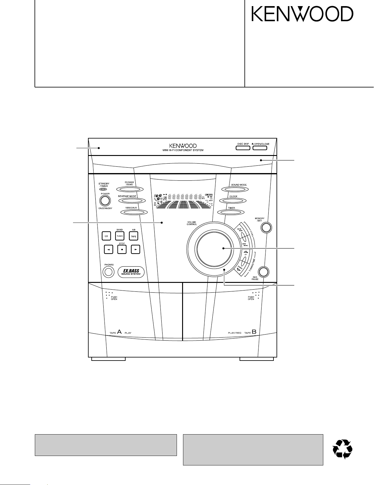
Panel ass'y
(A60-2091-08)
© 2001-4/B51-5713-00 (K/K) 1382
Panel(CD)
(A60-2090-08)
Front glass *
(B10-)
Knob(VOLUME)
(K27-2470-08)
Dress ring
(A21-3957-08)
In compliance with Federal Regulations, following are reproduction of labels on, or inside the porduct relating to laser product safety.
* Refer to parts list on page 33.
KENWOOD-Crop. certifies this equipment conforms to DHHS
Regulations No.21 CFR 1040. 10, Chapter 1, subchapter J.
DANGER : Laser radiation when open and interlock defeated.
AVOID DIRECT EXPOSURE TO BEAM.
RXD-A55/A75
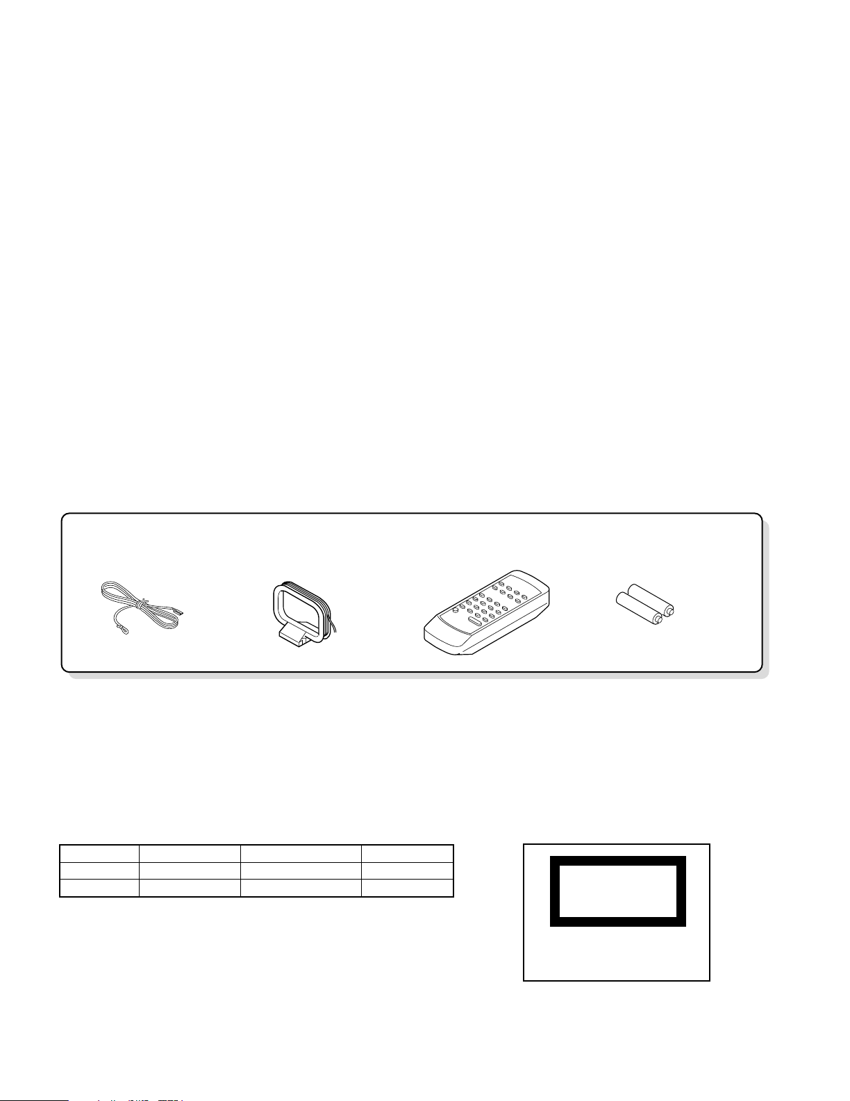
FM Antenna (1)
(T90-0883-08)
AM Loop Antenna (1)
(T90-0879-08)
Remote Control (1)
(A70-1531-08)
"AA" size battery (UM/SUM-3,
R6, HP-7 or similar)(2)
The marking this product has been
classified as Class 1. It means that there
is no danger of hazardous radiati
outside the product.
CONTENTS / ACCESSORIES
Contents
CONTENTS / ACCESSORIES .................................. 2
EXTERNAL VIEW .......................................................3
DISASSEMBLY FOR REPAIR....................................4
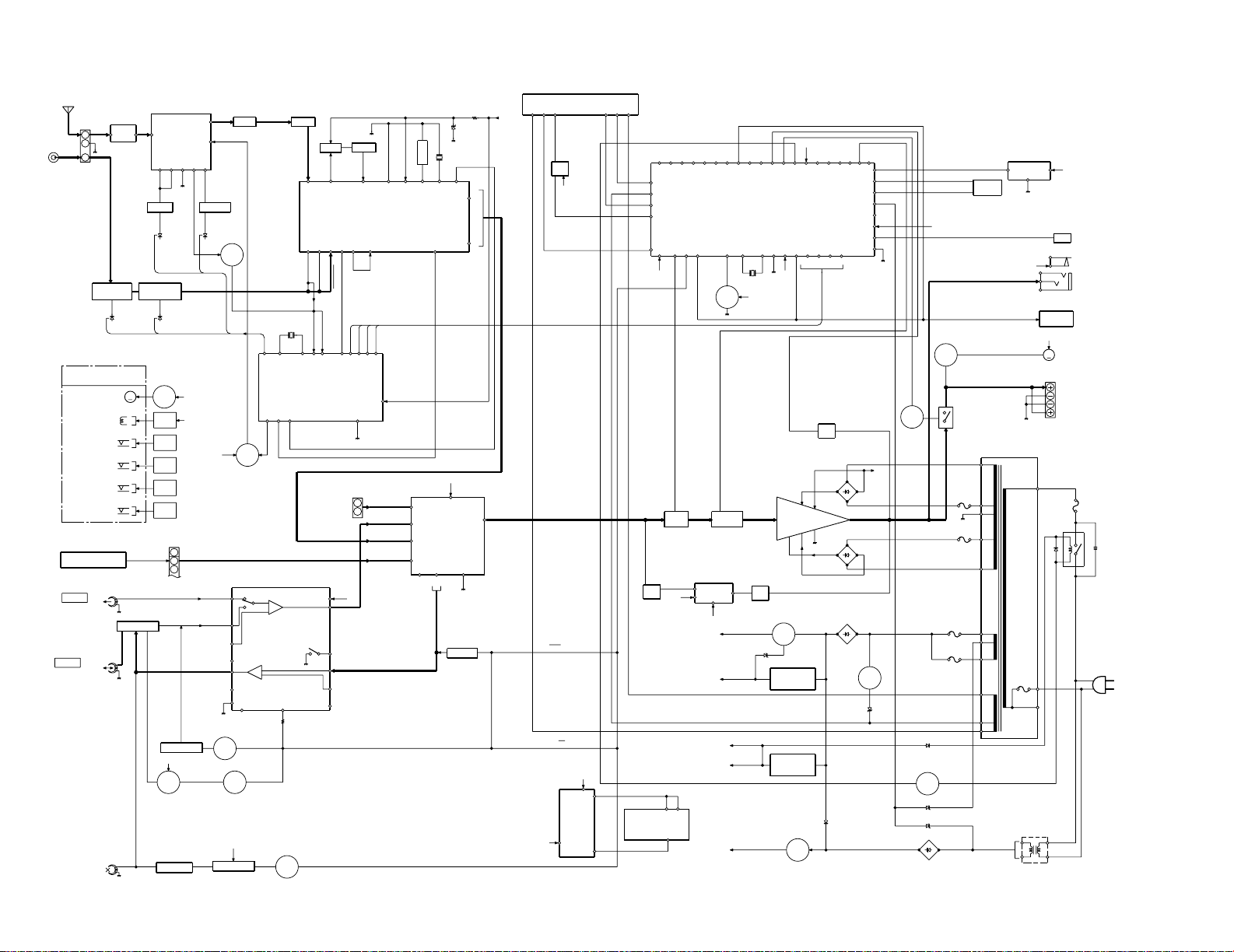
BLOCK DIAGRAM ......................................................9
CIRCUIT DESCRIPTION ..........................................11
ADJUSTMENT ..........................................................14
PC BOARD .............................................................. 16
SCHEMATIC DIAGRAM .......................................... 23
EXPLODED VIEW ....................................................31
PARTS LIST..............................................................33
SPECIFICATIONS ....................................................37
Accessories
SYSTEM CONFIGURATION Cautions
SYSTEM MAIN UNIT DESTINATION SPEAKER
XD-A55 RXD-A55 KP LS-N50S
XD-A75 RXD-A75 KP LS-N70S
LASER PRODUCT
CLASS 1
2
ANTENNA
FM
75Ω
AM LOOP
R
SPEAKERS
++-
RL
-
VIDEO
/AUX
L
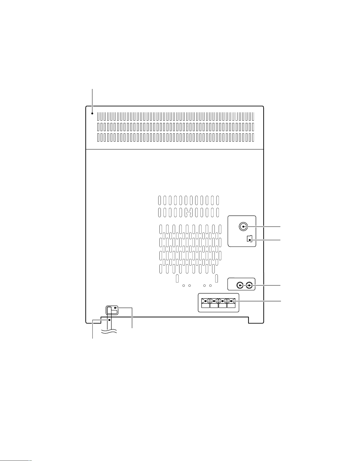
Cabinet(TOP)
(A02-3014-08)
RXD-A55/A75
EXTERNAL VIEW
AC power cord
(E30-7222-08)
AC power cord bushing
(J42-0351-08)
FM Antenna
(E70-0145-08)
Pin ass'y
(E40-8933-08)
Pin jack
(E63-1219-08)
Lock terminal board
(E70-0144-08)
3
Caution on Disassembly
Follow the below-mentioned notes when disassembling
the unit and reassembling it, to keep it safe and ensure
excellent performance:
1. Take cassette tape and compact disc out of the unit.
2. Be sure to remove the power supply plug from the wall
outlet before starting to disassemble the unit.
3. Take off nylon bands or wire holders where they need be
removed when disassembling the unit. After servicing
the unit, be sure to rearrange the leads where they were
before disassembling.
4. Take suffcient care on static electricity of integrated
circuits and other circuits when servicing.
Figure 7-2
Figure 7-3
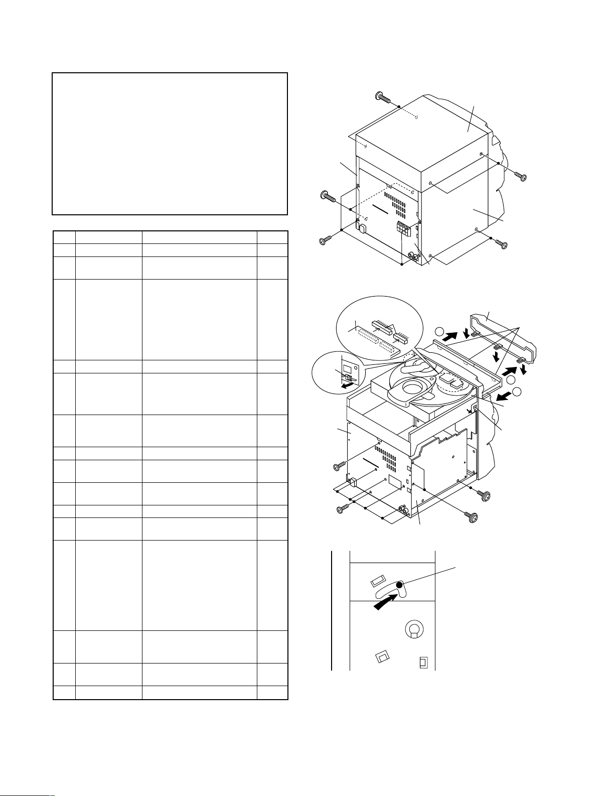
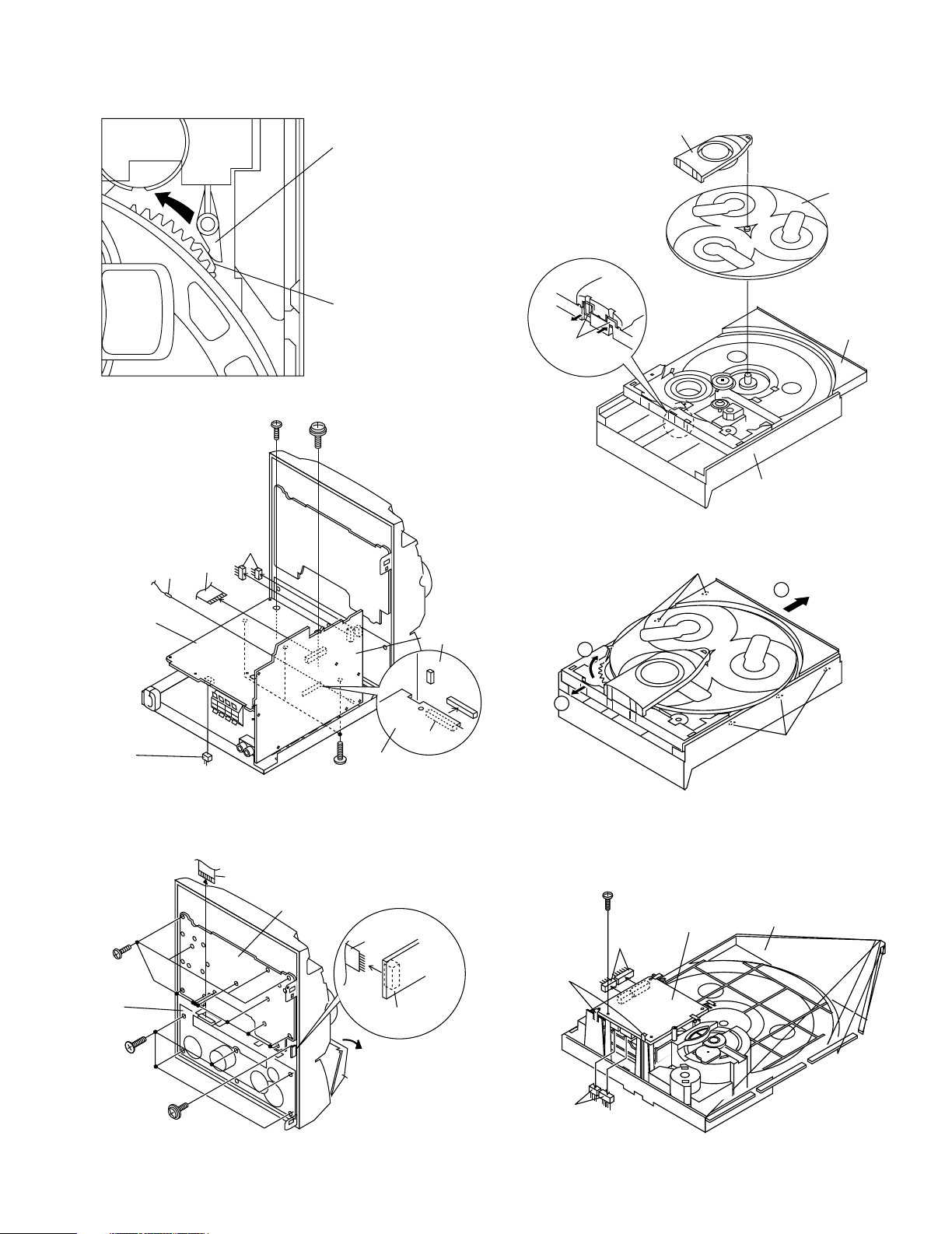
1 Top Cabinet 1. Screw ..................... (A1) x4 7-1
2 Side Panel 1. Screw ..................... (B1) x8 7-1
(Left/right)
3 CD Player Unit/ 1. Turn on the power supply, 7-2
CD Tray Cover open the disc tray, take out
the CD cover, and close.
(Note 1)
2. Screw ..................... (C1) x1
3. Hook ....................... (C2) x3
4. Hook ....................... (C3) x2
5. Socket .................... (C4) x2
4 Rear Panel 1. Screw ..................... (D1) x9 7-2
5 Main PWB 1. Screw ..................... (E1) x1 7-2
2. Socket .................... (E2) x3 8-2
3. Flat Cable .............. (E3) x1
4. Tip Wire .................. (E4) x1
6
Power Supply PWB
1. Screw ..................... (F1) x2 8-2
2. Socket .................... (F2) x1
3. Flat Wire................. (F3) x1 8-3
7 Front Panel 1. Screw ..................... (G1) x3 8-2
8 Display PWB 1. Screw .....................
(H1) x9
8-3
2. Socket .................... (H2) x1
9 Tape Mechanism 1. Open the cassette holder. 8-3
2. Screw...................... (J1) x5
10
Headphones PWB
1. Screw ..................... (K1) x1 8-3
11 Turntable 1. Hook ....................... (L1) x2 8-4
2. Cover ..................... (L2) x1
12 Disc Tray 1.
Turn fully the lock lever in the
7-3
arrow direction.
2.
While holding the lock lever,rotate
8-1
the cam gear until the cam gear
rib engages with the clamp lever.
3.
Push the slide holder backward to
8-5
engage the claw with the groove
and remove it in the direction
of the arrow. ..............
(M1) x6
13 CD Servo PWB 1. Screw ..................... (N1) x1 8-6
(Note 2) 2. Hook ....................... (N2) x2
3. Socket .................... (N3) x4
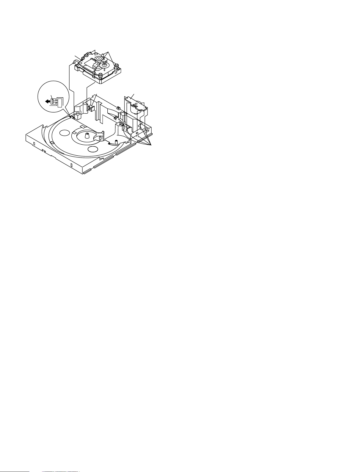
14 CD Mechanism 1. Hook ....................... (P1) x2 9-1
2. Hook ....................... (P2) x3
15
Loading Motor PWB
1. Hook ....................... (Q1) x5 9-1
STEP
REMOVAL PROCEDURE
FIGURE
Figure 7-1
Note 1:
How to open the changer manually. (Fig. 7-3)
1. In this state, turn fully the lock lever in the arrow direction
through the hole on the loading chassis bottom.
2.
While holding the lock lever, rotate the cam gear anticlockwise
until the cam gear rib engages with the clamp lever.
(Fig. 8-1)
3. After that, push forward the CD slide holder.
Note 2:
1. After removing the connector for the optical pickup from the
connector, wrap the conductive aluminium foil around the
front end of the connector so as to protect the optical pickup
from electrostatic damage.
Note 3:
1. Be careful not to break the claw of the CD mechanism.
2. When fining back the cam gear assembly, let it lock by front
movement.
RXD-A55/A75
DISASSEMBLY FOR REPAIR
4
Side Panel
(Right)
(B1)x2
ø3x10mm
(B1)x4
ø3x10mm
(C3) x1
Pull
Rear
Panel
(C1)x1
ø3x10mm
(D1)x7
ø3x10mm
(A1)x2
ø3x12mm
CD Servo
PWB
(C4)x2
Main PWB
Rear
Panel
1
(D1)x2
ø3x10mm
LOCK LEVER
Top Cabinet
DC Tray Cover
(E1)x1
ø3x10mm
(A1)x2
ø3x12mm
Side Panel
(Left)
(B1)x2
ø3x10mm
(C2) x3
1
2
CD Player
Unit
(C3)x1
RXD-A55/A75
Figure 8-1
Figure 8-2
Figure 8-3
Figure 8-4
Figure 8-5
Figure 8-6
CLAMP LEVER
CAM GEAR RIB
(F1)x1
ø3x6mm
(G1)x3
ø3x10mm
(F1)x1
ø3x10mm
(F2)x1
(E3)x1
(E4)x1
(E2)x2
Main PWB
(E2)x1
Power
Supply
PWB
Power
Supply
PWB
(H1)x9
ø3x10mm
(H2)x1
(J1)x5
ø3x10mm
(K1)x1
ø3x10mm
(F3)x1
Display PWB
Headphones
PWB
Open
Cassette
Holder
Tape
Mechanism
Turntable
Disc Tray
(L2) x1
CD Player Unit
(L1) x2
1
3
2
(M1) x3
(M1) x3
(N3) x2
(N2) x2
(N3) x2
CD Servo
PWB
CD Player
Base
(N1)x1
ø3x8mm
DISASSEMBLY FOR REPAIR
5
RXD-A55/A75
Figure 9-1
(P2) x3
(P1) x1
(Q1) x5
(P1) x1
Loading
Motor
PWB
CD
Mechanism
DISASSEMBLY FOR REPAIR
6
DISASSEMBLY FOR REPAIR
REMOVING AND REINSTALLING THE MAIN PARTS
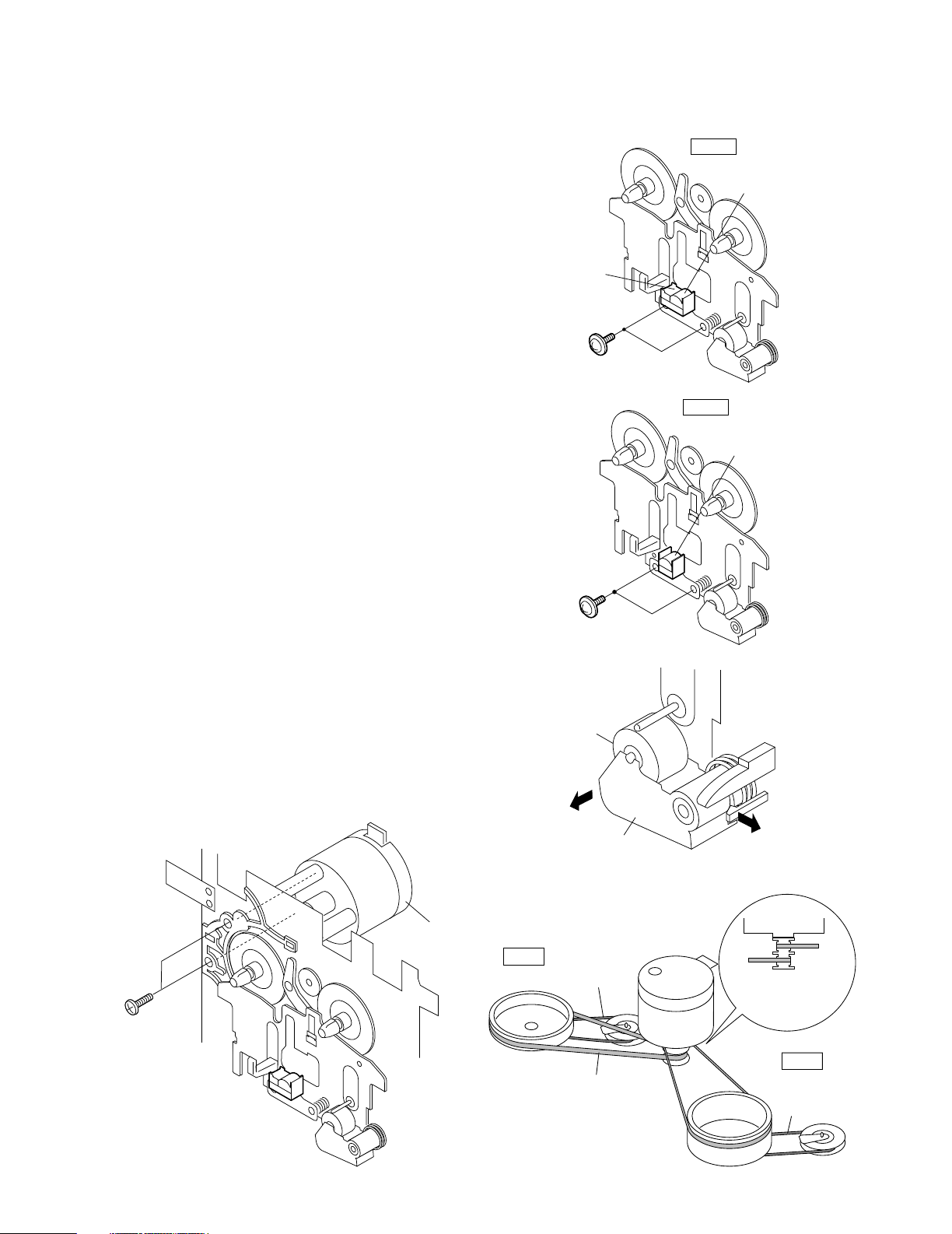
TAPE MECHANISM SECTION
Perform steps 1 to 7 and 9 of the disassembly method to
remove the tape mechanism.
How to remove the record/playback and erase
heads (TAPE 2) (See Fig. 10-1)
1. When you remove the screw (A1) x 2 pcs., the recording/
playback head and three-dimensional head of the erasing
head can be removesd.
How to remove the playback head (TAPE 1)
(See Fig. 10-2)
1. When you remove the screw (B1) x 2 pcs., the playback
head.
How to remove the pinch roller (TAPE 1/2)
(See Fig. 10-3)
1. Carefully push the inside claw to remove it. The pinch roller
pawl in the direction of the arrow <A>, and remove the pinch
roller (C1) upwards.
Note:
When installing the pinch roller, pay attention to the spring
mounting position.
How to remove the belt (TAPE 1) (See Fig. 10-4)
1. Remove the main belt (D1) x 1 pc., from the motor side.
2. Remove the FF/REW belt (D2) x 1 pc.
How to remove the belt (TAPE 2) (See Fig. 10-4)
1. Remove the main belt (E1) x 1 pc., from the motor side.
2. Remove the FF/REW belt (E2) x 1 pc.
How to remove the motor (See Fig. 10-5)
1. Remove the screws (F1) x 2 pcs., to remove the motor.
Figure 10-1
Figure 10-2
Figure 10-3
Figure 10-4Figure 10-5
TAPE2
TAPE1
Main Belt
(D1)x1
TAPE2
Main Belt
(E1)x1
TAPE1
Main Belt
FF/REW
Belt
(E2)x1
FF/REW
Belt
(D2)x1
Motor
Motor
(A1)x2
Ø2x9mm
TAPE2
Record/Playback
Head
Erase Head
(B1)x2
Ø2x9mm
TAPE1
Playback
Head
Pinch Roller
(C1)x1
<A>
STEP1
STEP2
(F1) x2
Ø2.6x5mm
Motor
RXD-A55/A75
7
RXD-A55/A75
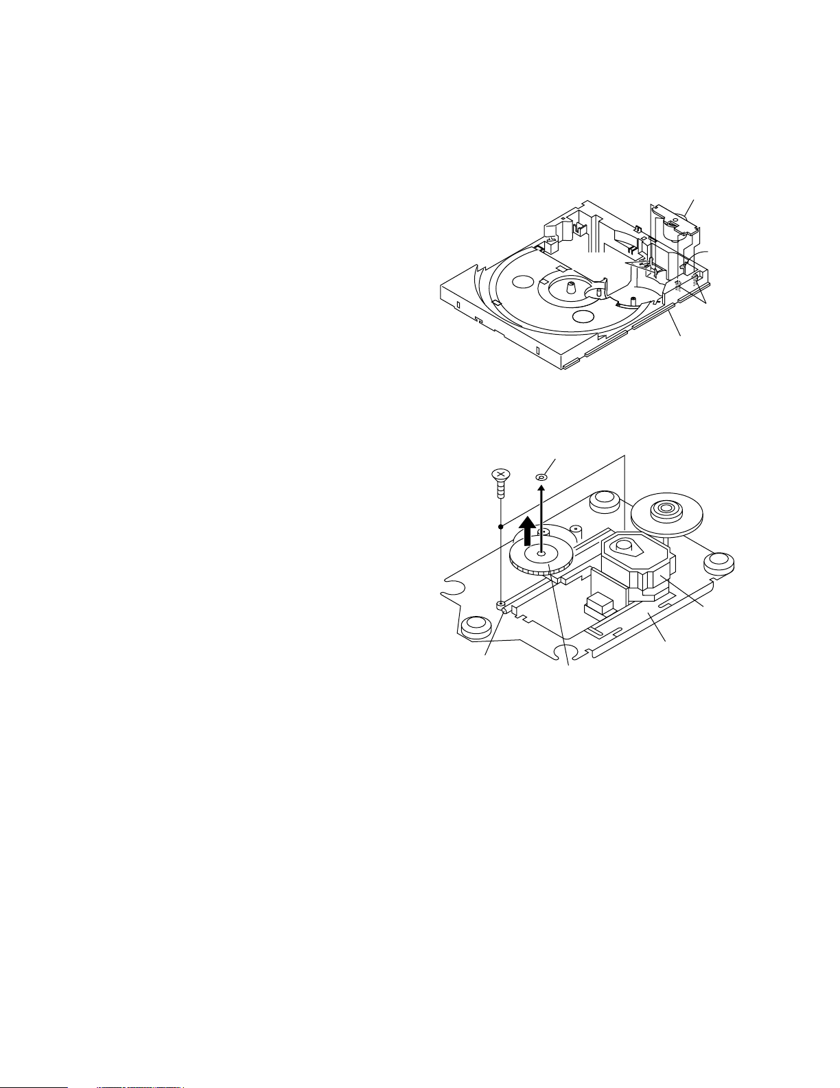
How to remove the pickup (See Fig. 11-2)
1. Remove the stop washer (B1) x 1 pc., to remove the gear
(B2).
2. Remove the screws (B3) x 2 pcs., to remove the shaft (B4).
3. Remove the pickup.
Figure 11-2
CD MECHANISM SECTION
Perform steps 1, 2, 3, 11 and 14 of the disassembly method
to remove the CD mechanism.
How to remove the loading motor
(See Fig. 11-1)
1. Bend the hooks (A1) x 5 pcs., to remove the loading motor.
Figure 11-1
Note
After removing the connector for the optical pickup from the
connector wrap the conductive aluminium foil around the front
end of connector so as to protect the optical pickup from
electrostatic damage.
DISASSEMBLY FOR REPAIR
Loading Moter
(B3) x2
ø2.6 x6mm
(A1)x2
(A1)x1
(A1)x2
CD Base
Stop Washer
(B1) x1
Pickup
8
Shaft
(B4) x1
CD Mechanism
Gear
(B2) x1
345
1
3
2
T.F
1
2
3
8
1
6
9
7
23
24
7
18
21
15
14
12
16
8
4
1
2
9
5
17
13
AM MIX
AM IF
GND
VCC
FM DET
VCO
MO/ST
L
R
AM OSC IN
AM OSC OUT
FM/AM OUT
AM RF IN
STEREO
MPXIN
FM/AM
10
7
9
21
20
1
MO/ST
FM/AM
11
152216
17
VDO
345
6
OSC
4.5MHz
X352
+B4
CE
DI
CL
DO
1
3
2
9
10
7
16
15
13
12
14
11
R
L
R
L
R
L
R
L
17
3
+B4
FM
OSC
AM IN
FM IN
VT
FM OSC
FM
FM+B
214R
L
8
18
AUX
TAPE
CD
TUNER
L
R
23
+B4
R
L
24
2
3
4
6
9
16
T1/T2
REC
13
4
5
7
18
VCC
1
+5V
+B3
+B3
23
14
12
21
20
P.B
H/N
17
8
15
19
NOR/
HIGH
T1/T2
+B4
L
R
L
R
10
L NF
R NF
ALC
REF
R REC
R NF
L REC
POP REDUCE
R(T2)
L NF
R(T1)
L(T2)
L(T1)
+B4
+B4
REC
7
4
1
8
-B2
+B4
5
VH+
VH-
VL-
VL+
1418R
L
6
7
8,9
10,11
1
-B1
+B1
L-OUT
R-OUT
SP.DET.
12-14
25-36
15-24
4-11
1,2
38,39,50
10
4-6
7-9
1
2
21
56
58
59
575554
4950484746
43
42
67-78
79
80-89
90-92
93-100
52
53
51
45
44
41
40
38
39
36
37
25
33-31
34
35
11
16
13
12
17-20
+B7
+B7
+B7
+B7
+B7
VDD
VLOAD
RESET
VDO
22
23
24
CECLDO
DI
VDD
AVDO
+B6
BIAS
T1/T2
REC
1
2
3
+B7
+B3
+B6
R-CH
L-CH
+B2
-B2
+B3
M10V
+B4
A10V
VF2
+B4
63Hz
30
7
-B2
4
1
8
10Hz 1K
29
28
-VF
VF1
+B6
+5V
+B5
CD+B
C801
+B7
T1/T2
P.B
POWER AMP.
IC901
Q302
CNP301
AM
FM
BF301
B.P.F
FM FRONT END
TA7358AP
IC301
FM RF
L312 T301
FM OSC
T302
FM IF
CF303
COVERAGETRACKING
AM AM BAND
T303 T306
OSC BUFF
CF352
T351
CF351
IC302
FM IF DET./FM MPX./AM IF
LA1832S
X351
456kHz
ZD351
PLL(TUNER)
LC72131
IC303
Q360
CNS11
FROM CD SECTION
CNP1
LC75341
IC601
AUDIO PROCESSOR
JK601
VIDEO IN
M
IC101
Q703
Q704
Q705
54PIN
IC700
IC700
56PIN
53PIN
IC700
55PIN
IC700
MOTOR
DRIVER
TAPE MECHANISM
ASSEMBLY
SOLM1,SOLM2
SOLENOID
MM1
MOTOR
TAPE
SWM2
T2 PLAY
R.PLAY
SWM4
SWM1
T1 PLAY
SWM3
F.PLAY
AN7345K
/PLAYBACK AMP.
PLAYBACK AND RECORD
Rch
Lch
Rch
Lch
TAPE 1
TAPE2
PB HEAD
REC/PB HEAD
SWITCHING
Q103-106
SWITCHING
Q107,108
AC BIAS
Q111
Q109
Q126
Q110
SWITCHING
Q121,122
MUTING
SWITCHING
ERASE
HEAD
L104Q128
BIAS OSC
SWITCHING
Q124
BIAS
AM IF
Q862,863
IC860
KIA4558P
OPE AMP.
-2ODB
ATT
SYSTEM
MUTE
Q603,604 Q605,606
Q864,865
Q901-904
FL701
DISPLAY
IC700(1/2)
SYSTEM
UPD 780206
Q710-712
Q701-703
MICROCOMPUTER
Q700
RESET
XL701
4.1943MHz
P-IN
JOG701
JOG
RX701
SENSOR
REMOCON
KEY
TO CD
SECTION
JK670
HEADPHONES
M
M901
FAN MOTOR
Q907
DRIVER
Q905
RL901
SO901
TERMINAL
SPEAKER
D809
T801
TRANSFORMER
F804
5A/125V
F805
5A/125V
D810
D811-814
Q803
Q850
F806
CONSTANT
VOLTAGE
2A/125V
KIA7810AP
REGULATOR
VOLTAGE
Q851
VOLTAGE
CONSTANT
ZD851
2A/125V
F807
KIA4558P
MICROCOMPUTER
IC700(2/2)
OPE
AMP.
IC561,562
SYSTEM
UPD 780206
ZD801
REGULATOR
KIA7805P
VOLTAGE
Q852
Q802
Q801
D804
D803
5A/125V
F801
D801
CONSTANT
REGULATOR
VOLTAGE
D802-805
T802
SUB POWER
TRANSFORMER
RY801
AC POWER
SUPPLY CORD
AC 120V 60Hz
UNSWITCH 5V
SWITCHING
MAIN POWER
RXD-A75/A55
9
BLOCK DIAGRAM
RXD-A55/A75
10
FOCUS COIL
TRACKING COIL
FD0
TD0
SLDO
SPDO
20
22
21
26
XOUT
WRQ
DO
RES
DI
CE
CONT5
193728
50
56
75
RFVDD
VVDD
VDD
ADAVDD
FIN1
RVDD
LVDD
XVDD
FIN2
LDS
LDD
TIN2
TIN1
CLK
XIN
23
40
51
55
57
69
49
48
666564
636162
5
7
28
18
7
46
41
47
80
10
79
9
8
42
43
45
44
25
70
71
LCHO
LVSS
RCHO
RVSS
CONT2
CONT3
CONT4
+3.3V
+3.3V
4
5
7
6
1823244082
VCC1
VCC2
VCC4
VCC3
1
2
25
17
39
38
42
41
8-14
22
29-35
15
16
27
26
21
+5V
1
2
3
4
5
6
AGND
R-CH
DGND
L-CH
+5V
+5V
DO
4
6
5
DI
CLK
3
2
1
CE
WRQ
DRF
8
9
7
OC. DISC NO
CLAMP SW
CD RES
4
5
6
1
2
3
1
6
2
3
4
5
1
4
6
5
3
2
+5V
PICK UP UNIT
IC1
LC78645E
CONTROL
SERVO/SIGNAL
XL1
33.8688MHz
Q2
CONSTANT
VOLTAGE
Q1
LASER
DRIVER
IC2
M63001FP
DRIVER
FOCUS/TRACKING/SPIN/SLED
M
M
M1
MOTOR
SPINDLE
MOTOR
SLED
M2
PICKUP IN
Q3
CNP7
to
SECTION
MAIN
SECTION
CNP8
DISPLAY
to
CNP4 CNS4
M
SW1
OPEN/CLOSE
SW2
CLAMP
DISC
SW3
NUMBER
LOADING
RXD-A75/A55
RXD-A55/A75
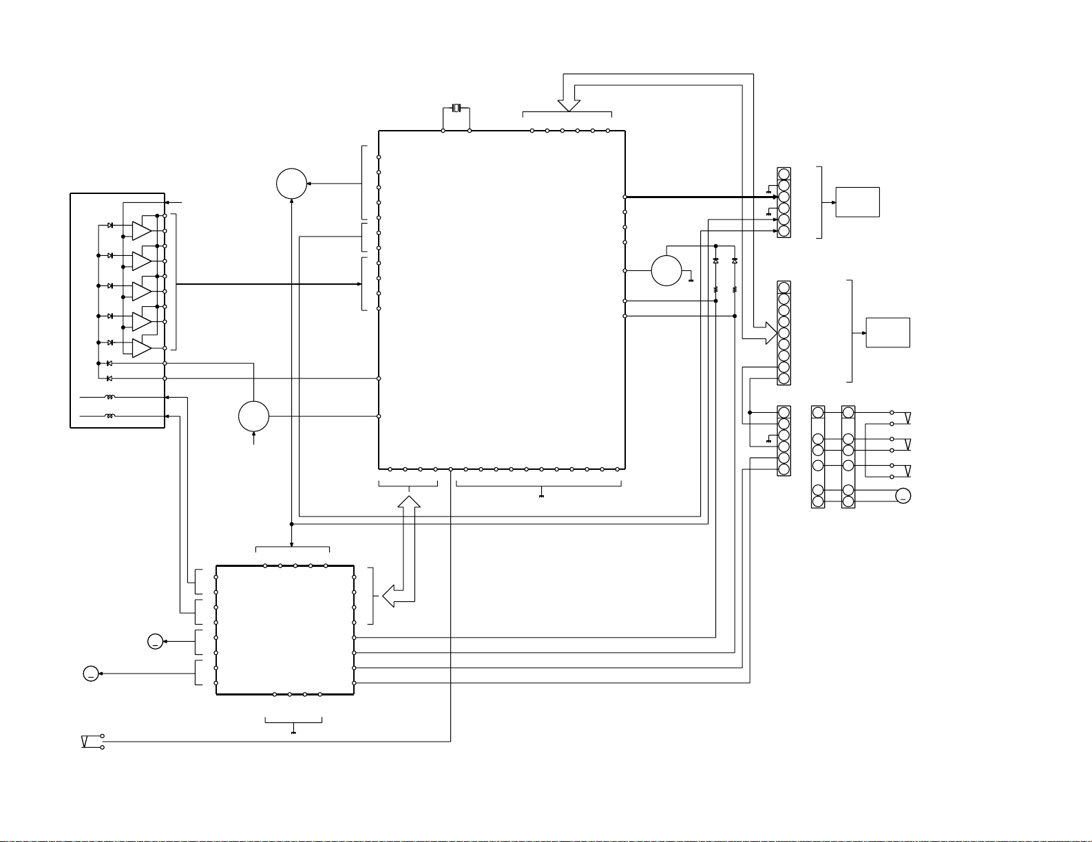
BLOCK DIAGRAM
RXD-A55/A75
CIRCUIT DESCRIPTION
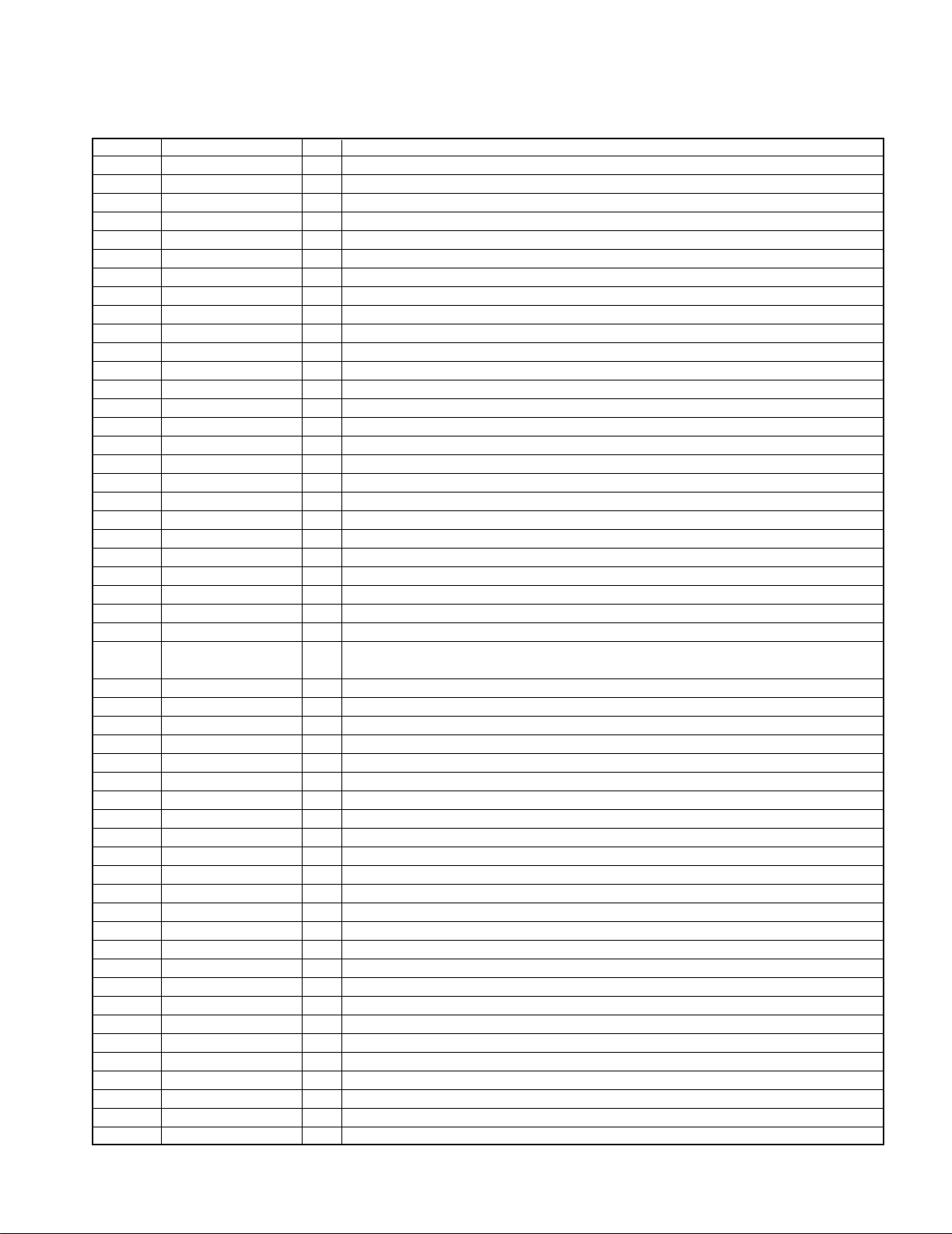
1. Port Description of Microprocessor
Port No. Port Name I/O Function
1 VDD - POWER SUPPLY(+5V)
2 -20dB ATT O -20dB ATTENUATION
3 NO USE/DSA STB - GND
4 T BIAS O DECK BIAS CONTROL
5 T T1/T2 O DECK T1/T2 CHANGE OVER
6 REC/PLAY O DECK RECORDING/PLAYBACK CHANGE OVER
7 RES OUT O CD DSP REQUEST
8 DRF I CDRF LEVEL DETECTION
9 WRQ I CD DSP WRITE REQUEST
10 REQUEST I RESET SIGNAL INPUT
11 X2 O MAIN CLOCK OUTPUT
12 X1 I MAIN CLOCK INPUT
13 VPP/IC - GND
14 XT2 - OPEN
15 SPN - OPEN
16 VDD - POWER SUPPLY(+5V)
17 CD CLK O CD DSP CLOCK
18 CD DI O CD DSP COMMAND
19 CD DO I CD DSP CODE Q INPUT
20 CD CE O CD DSP CE OUTPUT
21 CE O CHIP ENABLE OUTPUT
22 CLK O CLOCK OUTPUT
23 DI O DATA OUTPUT
24 DO I DATA INPUT
25 AVSS - GND
26 O/C SW/DSA DATA I CD OPEN CLOSE SWITCH INPUT
27
28 SPEANA 2 I SPEANA DATA INPUT(16kHz)
29 SPEANA 1 I SPEANA DATA INPUT(1kHz)
30 SPEANA 0 I SPEANA DATA INPUT(63kHz)
31~33 KEY2~KEY0 I KEY INPUT
34 AVDD - ANALOG POWER SUPPLY
35 AVREF - ANALOG REFERENCE VOLTAGE
36 P IN I POWER FAILURE DETECTION
37,38 JOG1,0 I JOG VOLUME INPUT 1, 0
39 REMOCON I REMOTE CONTROL SIGNAL INPUT
40 VSS - GND
41 SMUTE O SYSTEM MUTE CONTROL
42 T SOL B O DECK2 SOLENOID CONTROL
43 T SOL A O DECK1 SOLENOID CONTROL
44 T MOTOR O DECK MOTOR CONTROL
45 TIMER LED O TIMER LED CONTROL
46 VDD - POWER SUPPLY(+5V)
47 AC RLY CONT. O AC RELAY CONTROL
48 SP RLY O SPEAKER OUTPUT RELAY CONTROL
49 SP DET I SPEAKER OUTPUT DETECTION
50 T1 RUN I DECK1 REEL SENSOR DETECTION PORT
51 T2 RUN I DECK2 REEL SENSOR DETECTION PORT
52 CD CLAMP SW I CD CHANGER CLAMP SWITCH INPUT
53 PLAY SW A I DECK PLAY SWITCH A INPUT
54 PLAY SW B I DECK PLAY SWITCH B INPUT
55 FPA I DECK FORWARD RECORDING SWITCH INPUT
NO USE/DSA ACK
/TUN SM
- GND
11
 Loading...