

REGULATED DC POWER SUPPLY
PDS20-18/PDS36-10
PDS60-6
SERVICE MANUAL
KENWOOD TMI CORPORATION
© 1998-4/B51-1132-00 (K/K)
POWER
REGULATED DC POWER SUPPLY PDS36-10
0 +36V (10A)
-
+
PRESET
KEYLOCK/LOCAL
MEMCRY
VOLTAGE
CURRENT
FAST/SLOW
CC
CV
CVP
OUTPUT
8.8.8.8.
8.8.8.8.
0 +60V (6A)
GND
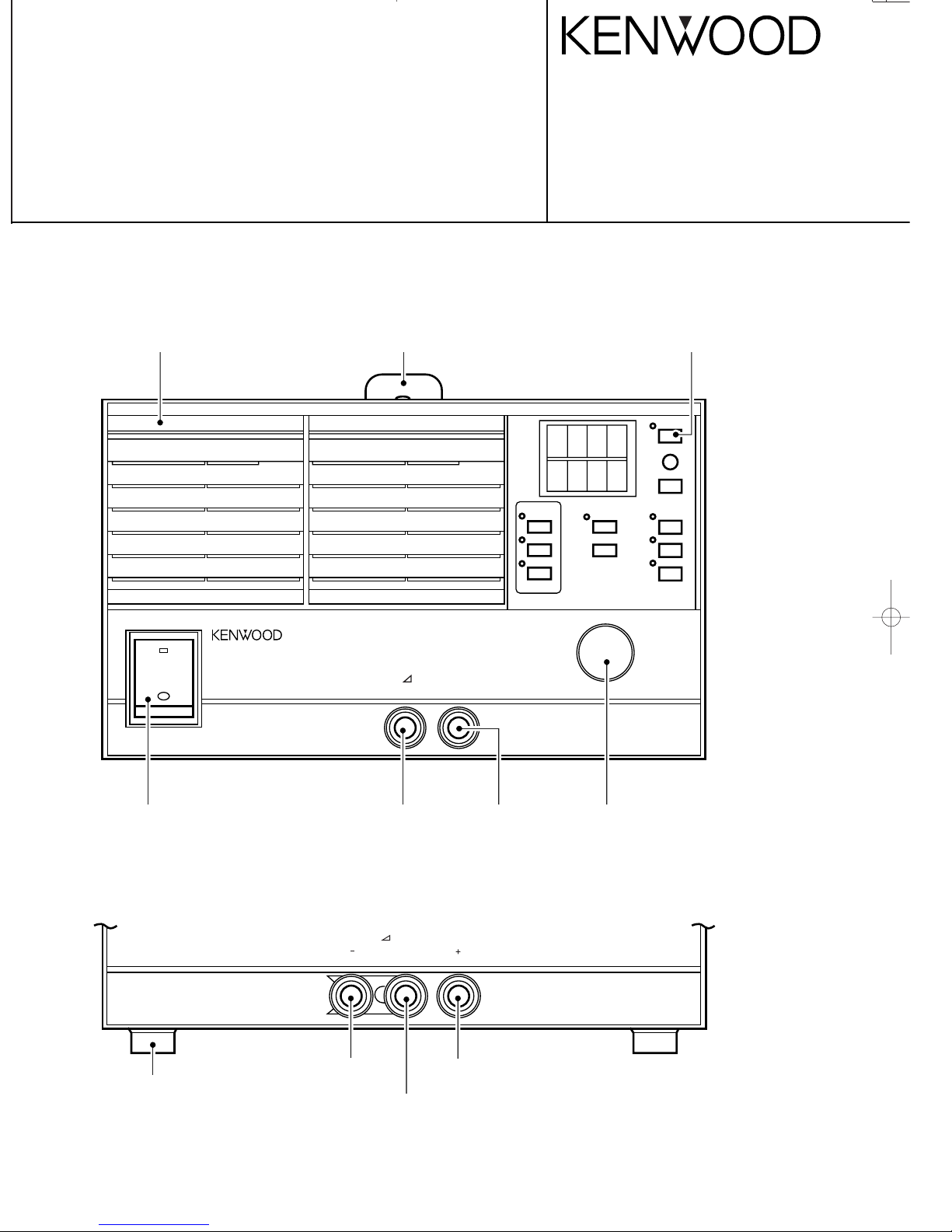
Front Panel
(PDS20-18 ; A63-0309-03)
(PDS36-10 ; A63-0311-03)
(PDS60-6 ; A63-0315-03)
Handle
(K01-0556-05)
Push Button
(K29-7204-04)
Circuit Protector
(S79-0625-05)
Terminal ; White
(E21-0807-03)
Terminal ; Red
(E21-0806-03)
Rubber Foot
(J02-0506-05)
Terminal ; White
(E21-0807-03)
Terminal ; Red
(E21-0806-03)
Terminal ; Black
(E21-0808-03)
Rotary Encoder
(K21-0911-04)

PDS20-18/PDS36-10/PDS60-6
2
The following instructions are for use by qualified personnel only. To avoid electric shock,
do not perform any servicing other than contained in the operating instructions unless you
are qualified to do so.
WARNING
CONTENTS
SPECIFICATIONS......................................................................................................... 3
CIRCUIT DESCRIPTION................................................................................................6
BLOCK DIAGRAM........................................................................................................11
ADJUSTMENT............................................................................................................. 18
PARTS LIST (UNIT)..................................................................................................... 21
PARTS LIST (ELECTRICAL)....................................................................................... 22
SCHEMATIC DIAGRAM .............................................................................................. 35
P.C. BOARD ................................................................................................................ 42
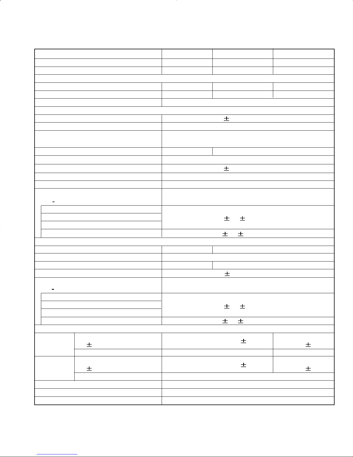
Model name PDS20-18 PDS36-10 PDS60-6
Rated output voltage (V) 20 36 60
Rated output current (A) 18 10 6
Output
Output voltage range (V) 0-20 0-36 0-60
Output current range (A) 0-18 0-10 0-6
Rated output power (W) 360
Constant voltage characteristics
Power regulation 0.005% +1 mV (for
10% source voltage fluctuation)
Load regulation 0.005% +2mV (for 0 to 100% fluctuation)
Ripple noise, p-p
(Measured with 20 MH z
oscilloscope)
30 mVp-p
Ripple noise, rms (5 Hz – 1 MHz) 1mVrms 1 mVrms
Transient response (typ.) 100 µsec
Temperature coefficient (typ.)
100 ppm/
°C
Rise time (typ.) Full load/no 100 msec/100msec
Fall time (typ.) Full load/no load 150msec/1000msec
Analog remote control setting
accuracy
(IF
30AN optional board is used)
External voltage (+ curve) : 0 to 10V
External voltage (- curve) : 10 to 0V
External resistance (+ curve) : 0 to
10kΩ
3% 50mV
External resistance (- curve) :10k to
0Ω
3% 100mV
Constant current characteristics
Power regulation 5mA 1mA
Load regulation 5mA
Ripple noise, rms (5 Hz – 1MHz) 10mArms 5mArms
Temperature coefficient (typ.)
100ppm/°C
Analog remote control setting
accuracy
(IF
30A optional board is used)
External voltage (+ curve) : 0 to 10V
External voltage (- curve) : 10 to 0V
External resistance (+ curve) : 0 to
10kΩ
3% 50mA
External resistance (- curve) :10k to
0Ω
3% 100mA
Meter and display
Display & accuracy
(23
5°C)
4 digits, LED, 0.1% rdg
2 digits
3 digits, LED,
0.1% rdg
2 digits
Voltmeter
Min. reading 10mV 100 mV
Display & accuracy
(23
5°C)
4 digits, LED, 0.5% rdg
2 digits
3 digits, LED,
0.5% rdg
2 digits
Ammeter
Min. reading 10mA
In constant voltage operation CV LED is lit.
In constant current operation CC LED is lit.
Output ON indicator OUTPUT LED is lit.
PDS20-18/PDS36-10/PDS60-6
SPECIFICATIONS
3
PDS20-18/PDS36-10/PDS60-6
4
SPECIFICATIONS
Model name PDS20-36 PDS36-20 PDS60-12
Output signals
In constant volt age operati on (opti on) Open collector , active Low
In constant current operation (option) Open collector, active Low
Alarm circuit operation Open collector, active Low
Output voltage monitor (option) 0 to 10 V, F.S.accuracy:
3%
Output current monitor (option) 0 to 10 V, F.S.accuracy:
3%
Operation func tions
OUTPUT key
Turns output on and off. Set to OFF automatically when power
is turned on. (Possible to select automatic ON setting.)
VOLTAGE key Changes output voltage using rotary encoder.
CURRENT key Changes output current using rotary encoder.
OVP key
Displays OVP circuit operating voltage on front panel,
which is variable between 10 and 110% of F.S.
KEY LOCK (LOCAL) key
Locks keys and knobs (except POWER switch).
Also remove remote control.
PRESET 1 – 3 keys
Used with MEM key to memorize three output voltage and
currents.
MEM key
Used with PRESET keys to memorize
three output voltage and currents.
FAST/SLOW key Changes output voltage and current setting speed.
ON/OFF control Enabled with input contact signals.
POWER switch shut-down Enabled with input contact signals
Output voltage remote sensing Compensates for 1 V voltage drop on single side.
Protector circuit
Output over
voltage (OVP)
Variable between 10 and 110% of F.S. Turns off
Input POWER switch when OVP functions.
Output over
current(OCP)
Turns off input POWER switch at 115% or more of F.S.
Overheat (OHP)
Turns off input POWER switch at internal heat sink
Temperature over preset value.
Soft OVP (OVD)
Set from external controller in remote control mode.
Output is turned off when soft OVP is active.
Environmental conditions [Indoor use only]
Altitude Up to 2000m
Overvoltage category
Pollution degree 2
Operating temp. range 0 to 40°C
Operating humid. range 30 to 80%RH
Storage temp. range -20 to 70°C
Storage humid. range 20 to 80%RH
To-GND volt age
250 Vdc
Coolicg method
Front air intake type forced air cooling
with fan motor insulation resistance
Insulation resistance
Chassis to power input 500Vdc, 30 MΩ or more
Chassis to output terminal 500Vdc, 20 MΩ or more
PDS20-18/PDS36-10/PDS60-6
5
SPECIFICATIONS
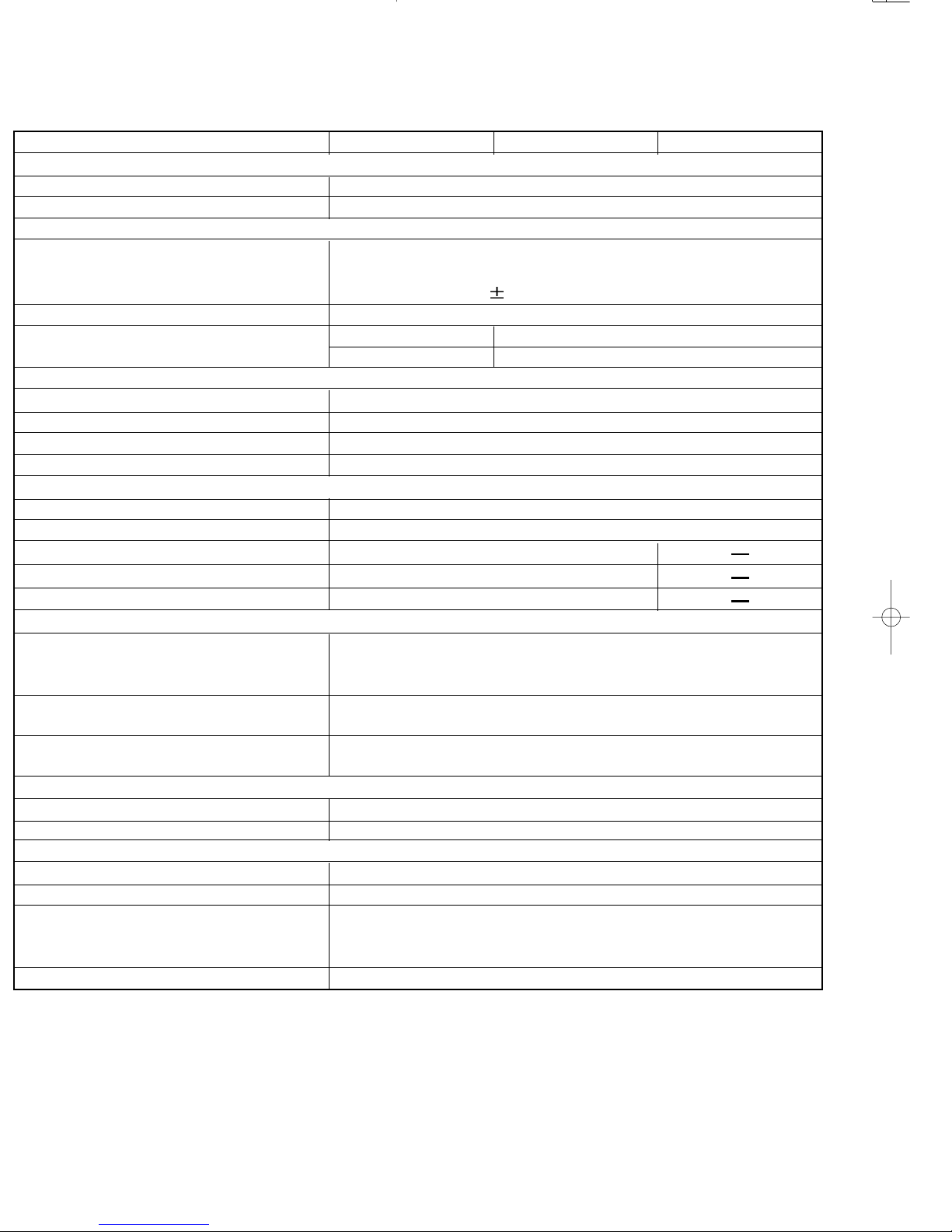
Model name PDS20-36 PDS36-20 PDS60-12
Dielectric strength
Chassis to power input 1.5 kVac, 1minute
Power input to output terminal 2.3 kVac 1 minute
Source voltage
Input voltage
100 to 240 Vac, 50/60 Hz single-phase
(this equipment is designed to operate
with
10% tolerance for rated voltage.)
Power factor (typ) 95%
560 W 520 W
Power consumption (typ)
600 V A 550 V A
Dimensions / Weight
Dimensi ons / Maximum dimensi ons
(W)
210 /210 mm
(H) 124 /124 mm
(D) 405 / 465.5 mm
Weight 6.3kg
Accessories
Instruction manual 1
Power cord 1 (3-core cable, 2 meters)
Output terminal protector
Cover : 1
GND cable
1
Egg-shape lug terminal
1
Options
Analog I/O board
Controls output voltage and current using external voltage and
resistance. Output monitored voltage and current and other
signals.
GP-IB board
Sets and reads back voltage and current,
turns on and off output. Reads back status.
RS-232C board
Sets and reads back voltage and current,
turns on and off output. Reads back status.
Output capacity extension
Collective parallel connection control Master-slave system, up to 3 units
Collective series connection control Master-slave system, up to 2 units
Regulatory information
LVD EN61010-1 & A2 (1995)
EMI EN55011 (1991) CLASS A
EMS
IEC801-2 (1991) 8 kVAD
IEC801-3 (1984) 3 V/m
IEC801-4 (1988)
Harmonic current Emission EN61000-3-2 (1995)

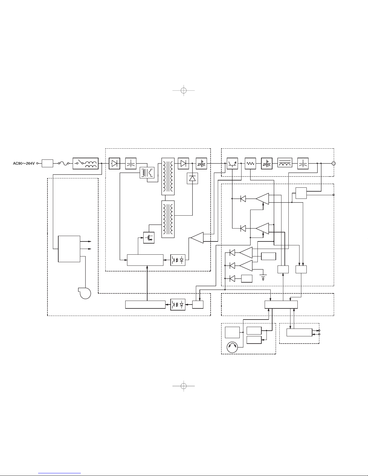
CONTROL UNIT (X77-2120)
Digital-to Analog Converter Circuit
Various signals received from the CPU unit are
isolated b y PH1 to PH4. Vari ous control s ignals
are output by IC4 to IC6. Data extracted b y IC10
and IC11 is input to IC12 (reference DAC) and IC14
(monitor DAC), which convert the data into analog
signals.
Voltage and current monitor signals and CV/CC
status and other status signals are input to IC7 and
IC 8 and is olated by PH5. The remote O UTPUT
ON/OFF signals from the rear panel are isolated by
PH6 and PH7 and returned to the CPU unit.
IC9 is the EEPROM for storing the calibration data,
data set on the panel, etc.
CV/CC Control Circuit
The v oltag e and cur rent refer ence volt age o utpu t
by IC12 is ab out +2 .8 V a t the f ull sc ale, w hich i s
ampl ifi er t o a bou t 5 B by a re fer enc e am pli fie r
consisting of IC106.
In t he C V op erat ion mod e, t he v olta ge m onit ore d
by means of + sensing is compared with this
reference voltage by R139, R137 and R225. The
error amplifier IC105-1/2 output the CV control
signal.
In the CC operation mode, the current monitor signal
detected b y the p ow er unit is compared w ith this
reference voltage b y R140 and R141. The error
amplifier IC105-2/2 output the CC control signal.
In the slave operation mode, a signal input from the
master unit is used as the reference signal for control.
The C V or C C control signal is s elected b y D113
and D114 and sent to the pow er unit driv e circuit.
The operation voltage is about –3V.
Voltage, Current and “OVP S et
Voltage”
Monitor Circuit
The voltage detected by means of + sensing is
output as the voltage monitor signal (about +2.8 V at
the full scale) by the monitor amplifier IC107-2/2.
The current monitor signal detected b y the p ow er
unit
is output as the current monitor signal (about +2.8 V
at the full scale) by the monitor amplifier IC107-1/2.
The OVP signal set on the panel is output as OVP
set voltage monitor signal (about +2.8 V at the
maximum voltage) through the buffer amplifier
IC103.
This monitor circuit is a sequential comparator circuit.
Output monitor signals are selected by IC15,
compared with the monitor reference signal from
IC14 (monitor DAC) by IC16, and then returned to
the CPU unit. The OVP set voltage monitor signal
can only be selected w hen the OVP key on the
panel is pressed.
Alarm Circuit
Several protector circuit are used : Variable
overvoltage (OVP), maximum overvoltage (MAX
OVP), pre overvoltage (PRE OVP), overcurrent
(OCP), overheat (OHP) and pre
overheat (PRE
OHP). The pre
overvoltage, overcurrent,
ovrtheat and pre
overheat protector circuits output
alarm signals when they detect abnormalities.
Voltage of about +2.8 V is produced by IC104 and is
div ided by the semi-fixed v ariabl e resis tor on the
panel to make the set reference voltage of the OVP
circuit. The voltage detected by a comparator circuit
consisting of IC101 by means of + sensing is
compared with the reference voltage.
An alarm is output if such comparison results in an
error. The MAX OVP circuit runs in the same way on
the –3 V reference voltage determined by D108.
Output alarm signals, except OHP, are latched by
IC108 and IC109. A trip signal activates the main
switch control circuit to turn off the main switch.
Other Circuit
The circuit consisting of Q110 to Q112 output
signals for turning on or off the bleeder circuit of the
power nit.
When the output is off and the output level has
lowered sufficiently, PH106 functions to turn off the
bleeder circuit. IC112 and IC113 produce
5 V for
the digital ICs and DACs from
15 V.
PDS20-18/PDS36-10/PDS60-6
6
CIRCUIT DESCRIPTION

PDS20-18/PDS36-10/PDS60-6
7
CIRCUIT DESCRIPTION
POWER UNIT (X68-1970)
Power Control Circuit
Q12 uses the control signals from the control unit
to control the current of the constant
current
circuit consisting of Q 13 and to drive Q 11. Q11
supplies the base current to Q1 to Q10.
The collector
emitter voltage of Q1 to Q10 is
detected and supplied as the Vce voltage to the
secondary voltage detector circuit of the AC unit.
Current Detector Circuit
R46 detects the output current. IC 2/2 amplifier it
as shown in Table 1 and outputs amplifier current to
the control unit. The current is reversed by IC1
1/2 and used as the reference current for the slave
side in the one control parallel operation mode.
Model Gain
20-18 33 time as high
36-10 33 time as high
60-6 36 time as high
Table 1
Bleeder Circuit
Two bleeder circuit are used : Input bleeder
circuit, and output bleeder circuit.
The input bleeder circuit has a constant current
circuit consisting of Q17 and Q19. It bleeds current
as shown in Table 2. When the voltage exceeds
value shown in Table 2, Q14 functions and reduces
the bleeder to about half. When the current
exceeds the ou tput current s how n in Tab le 2, the
comparator IC3
1/2 function and turns on Q16 to
deactivate the bleeder circuit.
The ou tput bleeder circuit has a constant
current
circuit consisting of Q20. It bleeds current as
show n in Table 3. It is turned on or off by the
bleeder signal output by the control unit.
Mo del
Input side
Bleeder current
Switching
Voltage
Off
Current
20 -18 Abou t 1 A Abou t 20 V Abou t 3.5 A
36 -10 Abou t 1 A Abou t 10 V Abou t 3 A
60-6 Abou t 0.5 A Abou t 30 V About 1.5
A
Table 2
Model Output side Bleeder current
20-18 About 150 mA
36-10 About 80 mA
60-6 About 50 mA
Table 3
Alarm Detector Circuit
This unit employs three alarm detector circuits : Pre
overvoltage, overcurrent, and overheat detector
circuits.
The pre overvoltage detector circuit has a
comparator IC4
1/2, which compares the input
voltage. When the input voltage exceeds the level
shown in Table 4, the circuit outputs an alarm signal.
The overcurrent detector circuit has a comparator
IC4 2/2, which outputs an alarm signal when the
current detected by IC1 exceeds about 115% of the
full scale level. The IC4
2/2 also serves as an
error amplifier and provides C C control when the
output current reaches about 115% of the full scale.
The overheat detector circuit has a TS1
thermal switch on the heat sink. This
switch
functions and circuit ou tputs an alarm signal w hen
the temperature exceeds about 110
.
Model Detection voltage
20-18 About 30V
36-10 About 50V
60-6 About 75V
Table 4

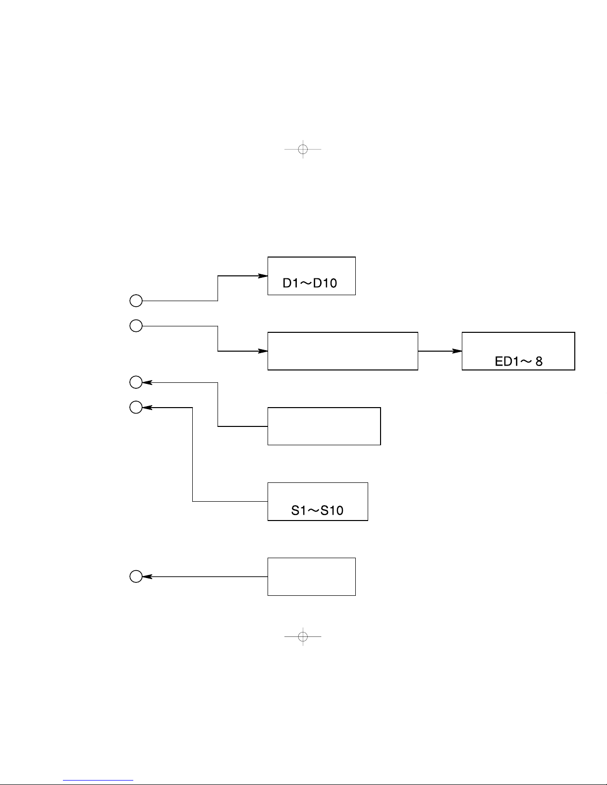
CPU UNIT (X77-2110)
CPU
IC7 (CPU) runs on 16 MHz clock pulses
generated by the X1 quartz oscillator.
Panel Switches (S1 to S10) and
Interruption Circuits (IC21 and IC22)
When any of the switches S1 to S10 on the panel is
p ressed, either i nput of the i nput port IC 9 goes
“High”. At that time, IC21 and IC22 cause an
interruption to the CPU.
Rotary Encoder ( S11 )
Signals to the rotary encoder are processed
by IC12, IC23 to IC25 and IC28 first.
Processed and output data is latched by
IC11 and input to the input port
(pins 17 and 15) of IC14.
A signal for clearing IC1 1 is output by the CPU in t he
program loop.
Input Ports (IC9 and IC14)
Three types of data and signals shown
below are input to the input ports , in addition
to signals from the panel switches and
encoder :
Serial data from the control unit
Signal issued when the OUTPUT switch is
turned
on
S
1)
2)
3)
1)
2)
ignal issued when the OUTPUT switch is
set to
the remote control position
These s ignals are read in the program loops and
sent to the CPU by IC9 and IC14.
Output Ports (IC10 to IC19)
IC16
The below-shown signals to the control unit ar e
ou tput from the IC 16 output port. These signals
are isolated by the control unit.
serial data to be sent to the D/A converter circuit
Clock pulses for operating various elements in
the
D/A converter circuit.
Strobe signals for controlling the D/A converter
circuit
IC17
Signals for the panel unit display driver
(IC1and IC2) are output by IC17.
IC18 and IC19
Signals for turning on the LEDs (D1 to D10) on the
p anel unit are outp ut b y IC 18 and IC 19 (p ins 18
and 19). Signals for controlling the flow of the RS232C
interface are output by IC19 (pin 12).
IC10
Signals for controlling various optional boards are
output by IC10.
Others
Reset signal
IC27 outputs a signal for resetting the CPU
when the POWER switch is turned on.
Driver
IC8 div ides 8 M Hz clock puls es output by the
CPU into 4 MHz pulses, which are output
from the IC10 port and used for optional
boards.
Panel unit X66-1600-00
IC1 and IC2 from a driver for the seven segment
LED indicator (ED1 to ED8). ED1 to ED8 are
controlled by signals output by IC17 (CPU
unit).
3)
PDS20-18/PDS36-10/PDS60-6
8
CIRCUIT DESCRIPTION

PDS20-18/PDS36-10/PDS60-6
9
CIRCUIT DESCRIPTION
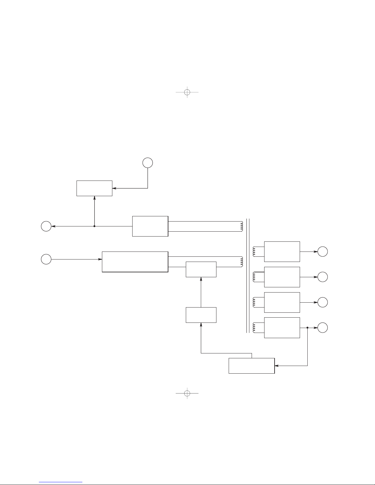
MO THER UNIT (X67-1420)
+15 V Rectifier and Smoother
A m o n g e l e c t r i c p o w e r t r a n s m i t t e d f r o m t h e
pri ma ry si de t hro ug h th e m ai n tra ns fo rme r (T 1) ,
this circuit produces rectified and smoothed +15 V to
be supplied to IC1 in the AC unit.
Main Power Primary Side Rectifier
and Smoother
Diode D1 rectifies AC power and capacitor C4
smoothes it.
Capacitor C4 stores voltage about 2 times as
high as the AC voltage.
Sub-Power Switching
Electric power having passed through diode D1 and
sto red in ca pac it or C4 pas ses t hro ugh th e s ub transformer (T1) and is switched by Q1 by mean s
of ringing choke conversion (RCC). The oscillation
frequency is about 60 kHz when the input AC
voltage is 100 V or about 120 kHz when the input
AC voltage
is 200 V. Q1 is controlled by signals
from the sub-
power control (D).
Sub-Power Control
PH1 and IC2 o utput signal s from the ci rcuit (J) fo r
det ect in g t he vo lta ge of th e int er nal +5 V po we r
(CPU unit). This sub-power control circuit controls
switching of Q1 based on such signals.
Internal -3.5 V Rectifier and Smoother
This circuit produces rectified and smoothed internal
vol ta ge of
3 .5 V at p ins 1 5 a nd 1 6 o f the s ub Tra ns fo rm er (T 1) , wh ic h s up pl ie d to th e po we r
Unit (X68-1970-0x) and control unit (X77-2120-0x).
Internal 15 V Rectifier and Smoother
Th i s c ir c u i t p r o d u ce s r e ct i f i e d a n d sm o o t h e d
Inte rnal vol tage of
15 V at pin s 10 to 12 o f th e
sub-transformer (T1), which is supplied to the
power
unit (X68-1970-0x) and control unit (X77-2120-0x).
Internal 15 V Rectifier and Smoother
Th i s c ir c u i t p r o d u ce s r e ct i f i e d a n d sm o o t h e d
In te rn al v ol ta ge o f
1 5 V a t pi ns 7 t o 9 of t h e
sub - T ra ns fo rm er (T 1) , wh ic h is su pp li ed t o th e
AC unit (X68-1980-0x).
Internal +5 V Rectifier and Smoother
Th i s c ir c u i t p r o d u ce s r e ct i f i e d a n d sm o o t h e d
Internal voltage of + 5 V a t pins 13 and 14 of the subTransformer (T1), which is supplied to the CPU unit
(X77-21 10-00).
Secondary Side Voltage Detector
This circuit detects voltage using R22 and R23 and
outputs control signals to the sub-power control (D)
throu gh PH 1 and IC2 in o rder to ma ke th e int erna l
+5 V constant.
Main Switch Control
Thi s c ir cui t shu ts do wn th e m ai n s wi tch t hro ug h
PH2 using the Trip+ signal from the control unit.

PDS20-18/PDS36-10/PDS60-6
10
CIRCUIT DESCRIPTION
AC UNIT (X68-1980)
Line Filter
This filter filtrates AC power and feeds filtrated
power to the primary side rectifier (B).
Main Power Primary Side Rectifier
Diode D4 in this rectifi er circ uit rect ifies AC voltag e
and s upp li es re ct if ied p owe r to th e ma in po we r
switching circuit (D).
Primary Side Current Detector
Th e p r im ar y s i de A C cu rr en t is d et ec te d at t hi s
transformer (T3) and fed to the control IC (IC1).
Main Power Switching
This main powe r swi tchi ng ci rcuit use s Q4 to Q 7
to switch AC voltage rectified by D4. Q4 to Q7 are
driven by Q 2 and Q 3 and controlled based on
signals output by IC1. The switching frequency is
about 135 kHz.
Main Power Control
The IC1-12(ON/OFF) terminal goes Low when t he
mai n o utp ut po wer i s o ff. It g oes Hi gh wh en th e
main output power is on. Signals for controlling Q2
and Q3 are output from the IC1-8 (OUT) terminal.
Triangular wave signals of the frequency decided
by R5 and C8 (about 135 kHz) are output from
IC1-15. IC1-3 (VDET) detects the Ac voltage. The
feed-back signal from PH3 for detecting the
secondary output Voltage is input to IC1-5. If IC14 (OVP) is set to Low, IC1-8 (OUT) is also set to
Low and oscillation stops.
Primary Side Input voltage Detector
This detector uses R14, R15 and R19 to detect the
primary AC voltage a nd output s signals controlle d
by IC100, PH100 and Q101 to the control IC (IC1).
Main Power Secondary Side
Rectifier and Smoother
This ci rcu it r ect ifi es and smo oth es elec tri c p owe r
transmitted by the primary side to the secondary
side through the main transformers T1 and T2.
Line Filter
This line filte r fil trate s DC volta ge ha v ing p ass e d
throug h the seco ndary side recti fier a nd sm oothe r
circuit (G) before it is supplied to the power unit.
Overheat Protector
This overheat protector circuit detects the
temperature of the heat sink on which Q4 to Q7 and
D4, D10 and D11 are mounted. When the
temperature exceeds about 1 10
, it is short-circuit,
resulting in an alarm.
Secondary Voltage Detector
This c ircui t cont rols the se conda ry out put v oltag e
based on the Vce voltage supplied by the power
unit (X68-1970-0x) and causes PH2 and PH3 to
output signals for making the Vce voltage of Q1 to
Q 10 of the p ow er unit constant to the control IC
(IC 1). S uch control is turned on or off b y the Vce
start controller block (K).
Vce Start Controller
This controller turns on or off the control for making
the Vce voltage constant using signals from the
control unit.
It turns off the control when the signal is set to High
or turns on the control when the signal is set to Low.
Table 5 below shows the Vce voltage of each type.
Model Vce voltage
20V About 3.5V
36V About 4.5V
60V About 4.5V
Table 5
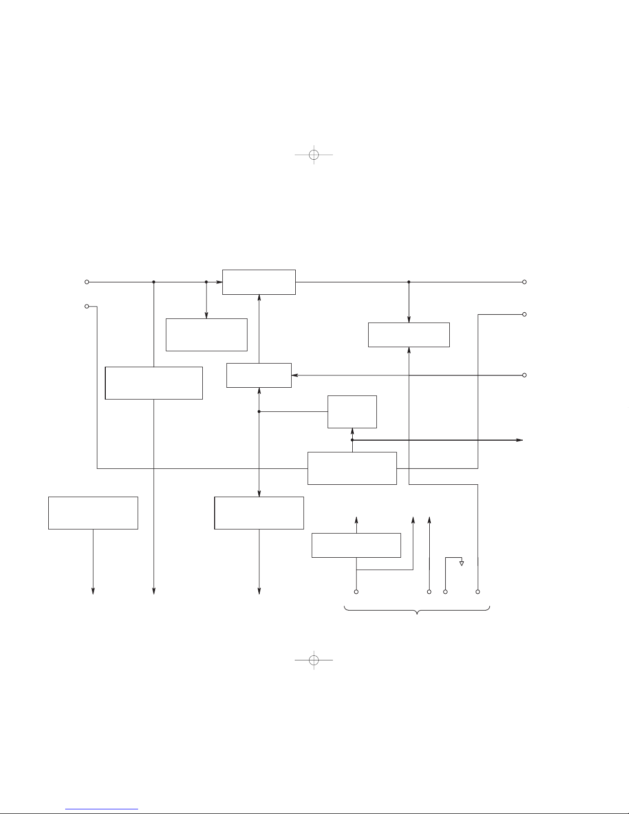
Primary Side
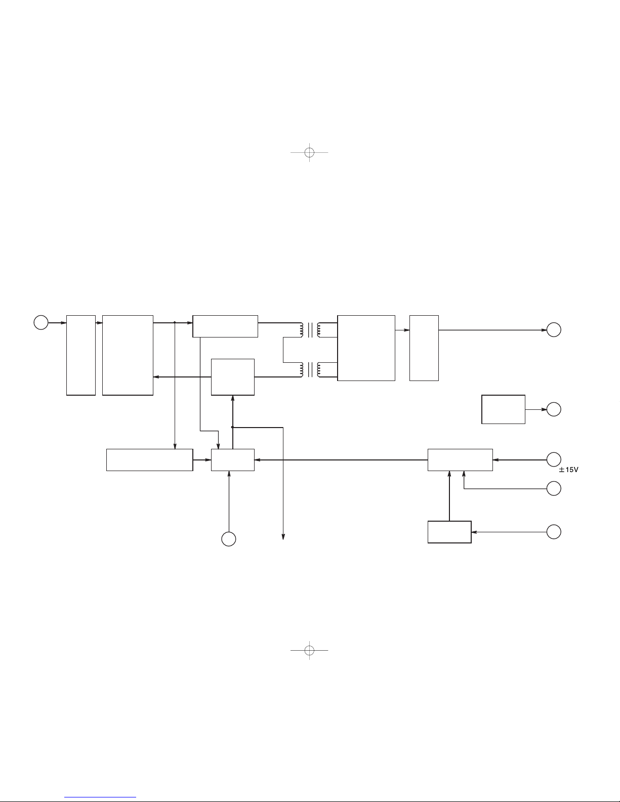
Control Circuit
ST2
ST1
VCE Detection
CT
SENSE
V OUT
OVP
OCP
A/D
Preset
D/A
Shunt
POWER SUPPLY UNIT
CONTROL UNIT
CPU UNIT
PANEL UNIT
MOTHER UNIT
OHP
CPU
I/O Control
I/O Option Board
I DISP
V DISP
Set Up
Switch
R/E
ALM
Sub Power
RCC
PRI
RSE
N/F
NFB
AC UNIT
CV
CC
R/L
S
Shut Down Circuit
FAN
VIN
PDS20-18/PDS36-10/PDS60-6
11
PDS BLOCK DIAGRAM
ENC
P_SW
LED
D-DRU
Set Up Volume
Switch LED
7-Segment LED Driver
IC1,2
Rotary Encoder
S11
Panel Switch
OVP Volume
VR1
7-Segment LED
CPU UNIT
PANEL UNIT (X66-1600-00)
(X77-2110-00)
CONTROL UNIT
(X77-2120-00)
PDS20-18/PDS36-10/PDS60-6
12
BLOCK DIAGRAM
Sub-Power
Switching
MAIN SWITCH
Control
MAIN AC
Main Power
Control
AC Unit
CPU Unit
Sub-Power
Control
Secondary Side
Voltage Detector
PH2,D3.4
IC1,D7.10
T1
Q1
Q2,PH1,D6
PH1,IC2
(C)
(D)
Trip +
Control Unit
(B) D1
(A)
Rectifier &
Smoother
Rectifier &
Smoother
Rectifier &
Smoother
Rectifier &
Smoother
Rectifier &
+ 15V
Smoother
Main Power Primary Side
Rectifier &
Smoother
D100
D11.12
D13.14
D5
(J)
(I)
(H)
(G)
(F)
Power &
Control Unit
Power &
Control Unit
MOTHER UNIT (X67-1420-0X)
PDS20-18/PDS36-10/PDS60-6
13
BLOCK DIAGRAM
Primary Overvoltage
Detection
IC4(1/2), Q18
Vce Voltage
(AC UNIT)
Primary Input
(AC UNIT)
Overcurrent
Detection Circuit
Q15
Drive Circuit
Power Control
Bleeder Circuit
Q14,16,17,19
Q1~10
Q11~13
IC3(1/2)
MAX CC
Error Amp
IC4(2/2)
Current Detection
Circuit
R46,IC1
Voltage Regulator
IC2
+5
+15 -15
Bleeder Circuit
Q20
Control
(CONTROL UNIT)
CC Monitor
(CONTROL UNIT)
OUTPUT-
OUTPUT +
+15 -15 GND -3.5V
MOTHER UNIT
OCP
Primary OVP
Overheat Detection
TS1
OHP
(CONTROL UNIT)
POWER SUPPLY UNIT (X68-1970-0X)
PDS20-18/PDS36-10/PDS60-6
14
BLOCK DIAGRAM
Secondary
Voltage Detector
Main Power
Switching
Main Power
Control
Primary Side
Input Voltage Detector
Primary Side
Current Detector
Line
Filter
Protector
Over
Heart
MAIN AC
T1
T2
+15V
Mother Unit
Vce Voltage
Power Unit
Mother Unit
Power Unit
Line
Filter
L3 D4
T3
Q4..7
D18.19.20 L5
IC1,PH1.2.3
IC100,PH100
(A)
(B) (C)
(D)
(F) (E)
(G) (H)
TS1
(I)
IC2,PH2.3
(J)
Q102.103.104,PH1
(K)
Vce Start
Controller
Start/Stop
Cnotrol Unit
Main Power
Secondary Side
Rectifier &
Smoother
Main Power
Primary Side
Rectifier
AC Unit
(X68-1980-01,03,05,07)
AC UNIT (X68-1980-00,02,04)
OHP
Power Unit
PDS20-18/PDS36-10/PDS60-6
15
BLOCK DIAGRAM
 Loading...