

Kenwood NX-320 Series Service Manual
UHF DIGITAL TRANSCEIVER
NX-320
SERVICE MANUAL
© 2011-3 PRINTED IN JA PAN
B51-8963-00 (N) 455
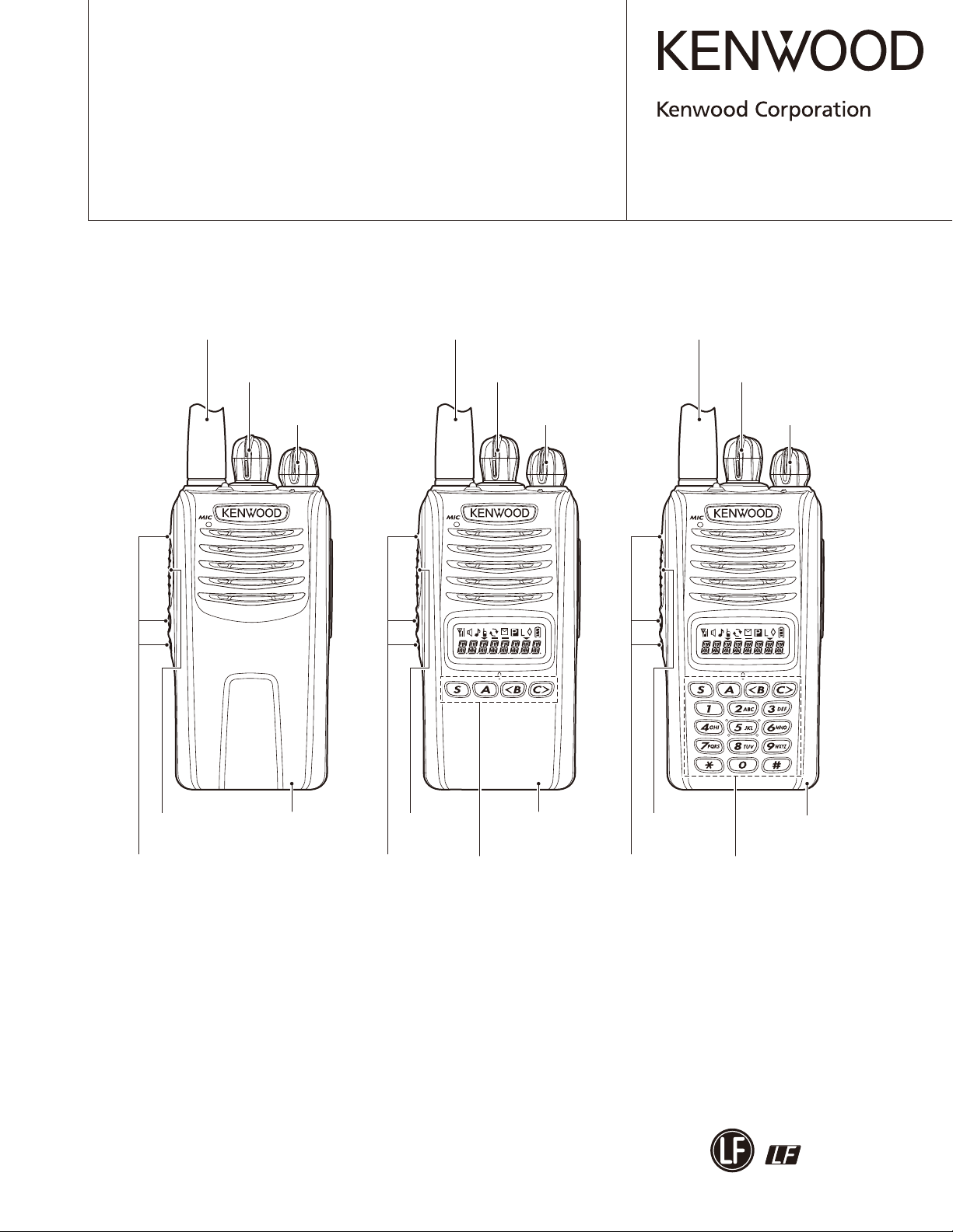
NX-320 K,K4,E3 NX-320 K2,K5,E2 NX-320 K3,K6,E
Helical antenna
(KRA-23: Option)
Knob (Selector)
(K29-9486-03)
Knob (Volume)
(K29-9485-03)
Helical antenna
(KRA-23: Option)
Knob (Selector)
(K29-9486-03)
Knob (Volume)
(K29-9485-03)
Helical antenna
(KRA-23: Option)
Knob (Selector)
(K29-9486-03)
Knob (Volume)
(K29-9485-03)
Knob (PTT)
(K29-9500-03)
Button knob
(Side1/Side2/AUX)
(K29-9501-03)
Plastic cabinet assy
(A02-4130-03)
Does not come with antenna.
Antenna is available as an option.
This product complies with the
directive for the European market.
RoHS
Knob (PTT)
(K29-9500-03)
Button knob
(Side1/Side2/AUX)
(K29-9501-03)
Plastic cabinet assy
(A02-4131-03)
Packing (4Key)
(G53-1864-01)
Knob (PTT)
(K29-9500-03)
Button knob
(Side1/Side2/AUX)
(K29-9501-03)
Plastic cabinet assy
(A02-4132-03)
Packing (16Key)
(G53-1865-01)
This product uses Lead Free solder.

NX-320
CONTENTS
GENERAL .....................................................3
SYSTEM SET-UP .........................................4
REALIGNMENT ...........................................5
DISASSEMBLY FOR REPAIR ......................8
CIRCUIT DESCRIPTION ............................12
COMPONENTS DESCRIPTION .................18
PARTS LIST ...............................................20
EXPLODED VIEW ......................................30
PACKING ....................................................31
TROUBLE SHOOTING ..............................32
ADJUSTMENT
K TYPE ....................................................35
E TYPE ....................................................54
TERMINAL FUNCTION .............................76
PC BOARD
DISPLAY UNIT (X54-3760-XX) ..............78
TX-RX UNIT (X57-8050-XX) ..................82
LEVEL DIAGRAM .....................................86
INTERCONNECTION DIAGRAM ..............87
SCHEMATIC DIAGRAM ............................88
BLOCK DIAGRAM ....................................98
OPTIONAL ACCESSORIES
KNB-55L (Li-ion Battery Pack) ............101
KNB-56N (Ni-MH Battery Pack) .........101
KNB-57L (Li-ion Battery Pack) ............101
SPECIFICATIONS ....................................102
Document Copyrights
Copyright 2011 by Kenwood Corporation. All rights re-
served.
No part of this manual may be reproduced, translated,
distributed, or transmitted in any form or by any means,
electronic, mechanical, photocopying, recording, or otherwise, for any purpose without the prior written permission
of Kenwood.
Disclaimer
While every precaution has been taken in the preparation
of this manual, Kenwood assumes no responsibility for errors or omissions. Neither is any liability assumed for damages resulting from the use of the information contained
herein. Kenwood reserves the right to make changes to any
products herein at any time for improvement purposes.
2
Firmware Copyrights
The title to and ownership of copyrights for firmware
embedded in Kenwood product memories are reserved for
Kenwood Corporation. Any modifying, reverse engineering, copy, reproducing or disclosing on an Internet website
of the firmware is strictly prohibited without prior written
consent of Kenwood Corporation. Furthermore, any reselling, assigning or transferring of the fi rmware is also strictly
prohibited without embedding the firmware in Kenwood
product memories.
Transceivers containing AMBE+2™ Vocoder:
The AMBE+2™ voice coding technology is embedded in
the fi rmware under the license of Digital Voice Systems, Inc.
GENERAL
NX-320
INTRODUCTION
SCOPE OF THIS MANUAL
This manual is intended for use by experienced technicians familiar with similar types of commercial grade communications equipment. It contains all required service
information for the equipment and is current as of the publication date. Changes which may occur after publication
are covered by either Service Bulletins or Manual Revisions.
These are issued as required.
ORDERING REPLACEMENT PARTS
When ordering replacement parts or equipment information, the full part identifi cation number should be included.
This applies to all parts : components, kits, or chassis. If the
part number is not known, include the chassis or kit number
of which it is a part, and a suffi cient description of the required component for proper identifi cation.
Model & Destination
(Market code)
NX-320
K
K2
K3
K4
K5
K6
E
E2
E3
Display unit X54-376X-XX
0-10 0-11 0-12 0-10 0-11
✓✓ ✓✓
✓ ✓ ✓✓✓
✓✓ ✓✓
✓ ✓ ✓✓✓
✓
✓✓ ✓✓
TX-RX unit X57-805X-XX
✓✓
✓✓
✓
PERSONAL SAFETY
The following precautions are recommended for personal
safety:
• DO NOT transmit until all RF connectors are verifi ed secure and any open connectors are properly terminated.
• SHUT OFF and DO NOT operate this equipment near
electrical blasting caps or in an explosive atmosphere.
• This equipment should be serviced by a qualifi ed technician only.
SERVICE
This transceiver is designed for easy servicing. Refer to
the schematic diagrams, printed circuit board views, and
alignment procedures contained within.
✓
✓
Frequency
range
450~
520MHz
400~
470MHz
Remarks LCD 4-key
–––
1st IF:
49.95MHz
LOC:
50.4MHz
–––
✓✓✓
–––
DTMF
keypad
–
–
–
3
NX-320
SYSTEM SET-UP
Merchandise received
License and frequency allocated by FCC
Choose the type of transceiver
Transceiver programming
Are you using the optional antenna?
NO
Are you using the speaker microphone?
NO
Type
NX-320 K
NX-320 K2
NX-320 K3
NX-320 K4
NX-320 K5
NX-320 E3
A personal computer, programming interface (KPG-22A/22U),
USB adapter (KCT-53U), and programming software (KPG-141D) are
required for programming.
(The frequency, and signaling data are programmed for the transceiver.)
YES
YES
KRA-23 or KRA-27
Optional antenna
KMC-21/KMC-45
Speaker microphone
GPS speaker microphone
Frequency range (MHz) RF power LCD 4-key
TX/RX 450~520
TX/RX 450~520
TX/RX 450~520
TX/RX 400~470
TX/RX 400~470
TX/RX 400~470 5WNX-320 K6
TX/RX 400~470 5WNX-320 E
TX/RX 400~470 5WNX-320 E2
TX/RX 400~470
(Option)
or
KMC-48GPS
(Option)
5W
5W
5W
5W
5W
5W
No
No No
Yes
Yes
Yes Yes
No
No
Yes
Yes
Yes
Yes
Yes
Yes
Yes
Yes
No
No
DTMF keypad
No
Yes
No
No
Yes
Yes
No
No
Delivery
4
REALIGNMENT
NX-320
1. Modes
User mode
Panel test mode *1
PC mode
Firmware
programming mode
Clone mode *1
Firmware version information *1
Mode Function
User mode For normal use.
Panel test mode *1
Panel tuning mode
PC mode
Data programming
mode
PC test mode
Firmware programming mode
Clone mode *1
Firmware version
information *1
*1 Used by the dealer to tune the transceiver.
Panel tuning mode *1
Data programming mode
PC test mode
Used by the dealer to check the fundamental characteristics.
Used for communication between the
transceiver and PC.
Used to read and write frequency data and
other features to and from the transceiver.
Used to check the transceiver using the PC.
This feature is included in the FPU.
Used when changing the main program of
the fl ash memory.
Used to transfer programming data from
one transceiver to another.
Used to confi rm the internal fi rmware version.
PC tuning mode
*1: K2,K3,K5,K6,E and E2 models only
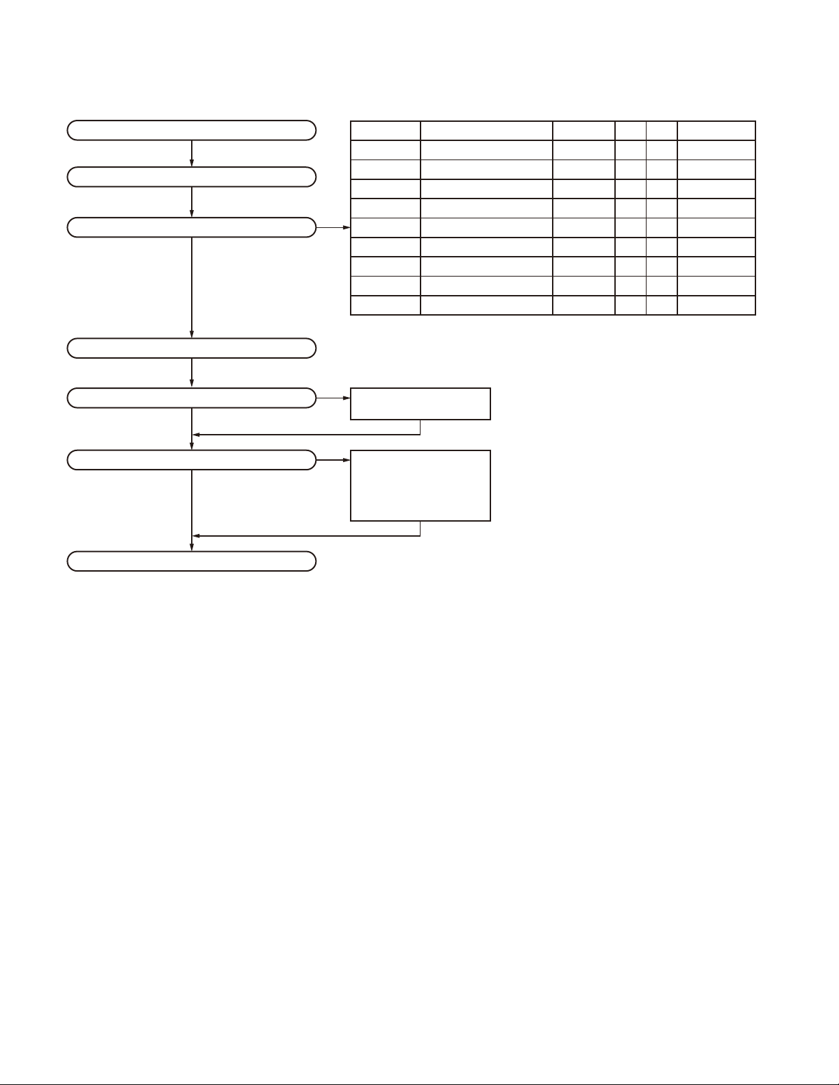
2. How to Enter Each Mode
Mode Operation
User mode Power ON
Panel test mode *2 [
PC mode Received commands from PC
Panel tuning mode *2 [Panel test mode] + [
Firmware programming mode [Side1] + Power ON
Clone mode *2 [
Firmware version information *2 [
*2: K2,K3,K5,K6,E and E2 models only
] + Power ON
]
] + Power ON
] + Power ON
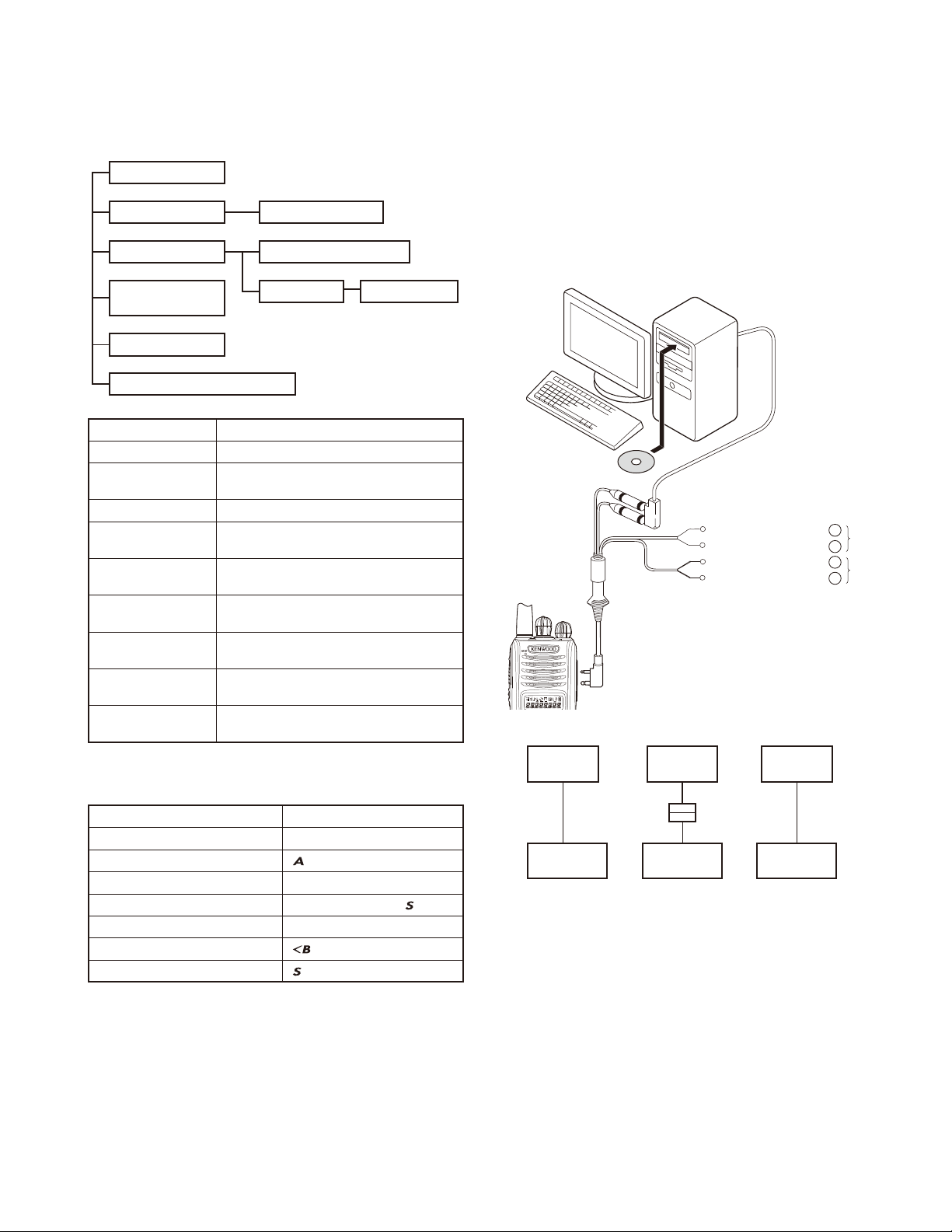
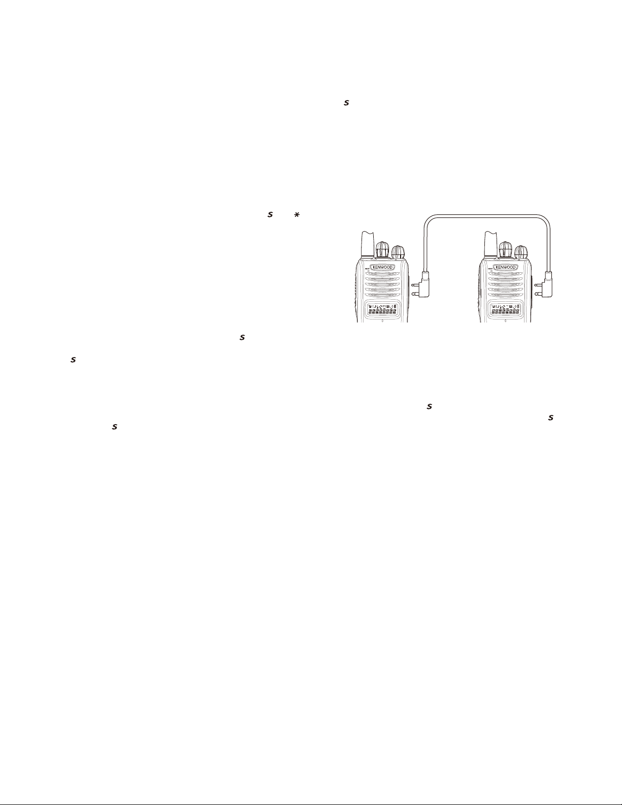
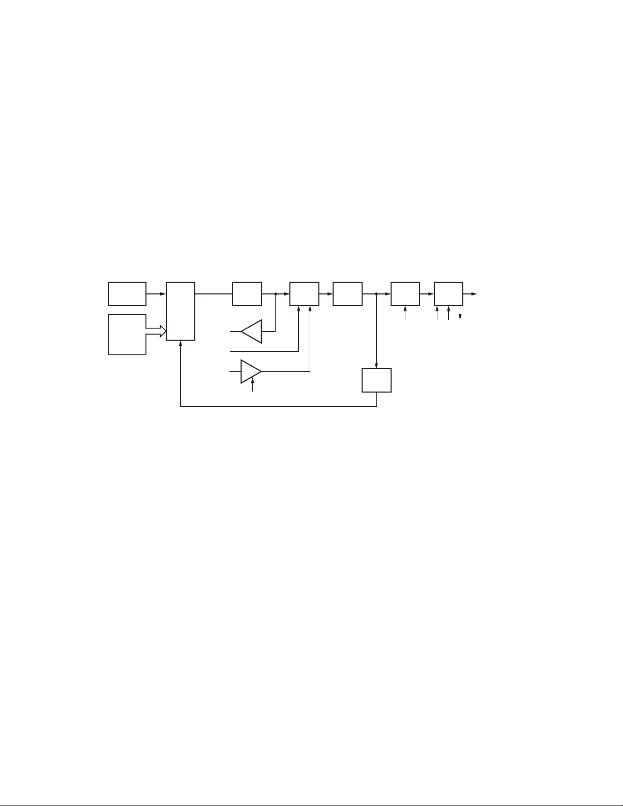
5. PC Mode
5-1. Preface
The transceiver is programmed by using a personal computer, programming interface (KPG-22A/22U), USB adapter
(KCT-53U) and programming software (KPG-141D).
The programming software can be used with a PC. Figure 1 shows the setup of a PC for programming.
PC
KPG-141D
Tuning cable
(E30-3216-05)
PC
D-SUB
(9-pin)
KPG-22A
Transceiver Transceiver
PC
USB
KCT-53U
KPG-22A
Transceiver
Fig. 1
5-2. Connection procedure
1. Connect the transceiver to the computer using the inter-
face cable and USB adapter (When the interface cable is
KPG-22A, the KCT-53U can be used.).
KPG-22A or KPG-22A
+KCT-53U or KPG-22U
Gray
Gray/Black
1.5D-XV Lead wire
1.5D-XV Shield wire
PC
USB
KPG-22U
+
SP
–
+
MIC
–
3. Panel Test Mode
(K2,K3,K5,K6,E and E2 models only)
Setting method refer to ADJUSTMENT.
4. Panel Tuning Mode
(K2,K3,K5,K6,E and E2 models only)
Setting method refer to ADJUSTMENT.
Note:
• You must install the KPG-22U driver in the computer to
use the USB programming interface cable (KPG-22U).
• You must install the KCT-53U driver in the computer to
use the USB adapter (KCT-53U).
• When using the USB adapter (KCT-53U) for the fi rst time,
plug the KCT-53U into a USB port on the computer with
the computer power ON.
5

NX-320
REALIGNMENT
2. When the POWER is switched on, you can immediately
enter user mode. When the PC sends a command, the
transceiver enters PC mode, and “PROGRAM” is displayed on the LCD.
When data is transmitting from the transceiver, the red
LED lights.
When data is receiving by the transceiver, the green LED
lights.
Note:
The data stored in the computer must match the “Model
Name” when it is written into the fl ash memory.
5-3. KPG-22A description
(PC programming interface cable: Option)
The KPG-22A is required to interface the transceiver to
the computer. It has a circuit in its D-sub connector case
that converts the RS-232C logic level to the TTL level.
The KPG-22A connects the SP/MIC connector of the
transceiver to the RS-232C serial port of the computer.
5-4. KPG-22U description
(USB programming interface cable: Option)
The KPG-22U is a cable which connects to a USB port on
a computer.
When using the KPG-22U, install the supplied CD-ROM
(with driver software) in the computer. The KPG-22U driver
runs under Windows XP, Vista or 7.
5-5. KCT-53U description (USB adapter: Option)
The KCT-53U is a cable which connects the KPG-22A to a
USB port on a computer.
When using the KCT-53U, install the supplied CD-ROM
(with driver software) in the computer. The KCT-53U driver
runs under Windows 2000, XP or Vista (32-bit).
5-6. Programming software KPG-141D description
The KPG-141D is the programming software for the trans-
ceiver supplied on a CD-ROM. This software runs under
Windows XP, Vista or 7 on a PC.
The data can be input to or read from the transceiver and
edited on the screen. The programmed or edited data can
be printed out. It is also possible to tune the transceiver.
6. Firmware Programming Mode
6-1. Preface
Flash memory is mounted on the transceiver. This allows
the transceiver to be upgraded when new features are released in the future. (For details on how to obtain the fi rmware, contact Customer Service.)
6-2. Connection procedure
Connect the transceiver to the personal computer using
the interface cable (KPG-22A/22U) and USB adapter (KCT53U: when the interface cable is KPG-22A, the KCT-53U can
be used.). (Connection is the same as in the PC Mode.)
6
6-3. Programming
1. Start up the firmware programming software (Fpro.exe
(ver. 6.0 or later)). The Fpro.exe exists in the KPG-141D
installed holder.
2. Set the communications speed (normally, 115200 bps)
and communications port in the confi guration item.
3. Set the fi rmware to be updated by File name item.
4. Press and hold the [Side1] key while turning the transceiver power ON. Then, the orange LED on the transceiver lights and “FIRM PRG” is displayed.
5. Check the connection between the transceiver and the
personal computer, and make sure that the transceiver is
in the Program mode.
6. Press “write” button in the window. When the transceiver starts to receive data, the [LOADING] display lights.
7. If writing ends successfully, the checksum is calculated
and a result is displayed.
8. If you want to continue programming other transceivers,
repeat steps 4 to 7.
6-4. Function
If you press the [Side1] key while “FIRM PRG” is dis-
played, the checksum is calculated, and a result is displayed.
If you press the [Side1] key again while the checksum is
displayed, “FIRM PRG” is redisplayed.
Note:
• This mode cannot be entered if the Firmware Programming mode is set to Disable in the Programming software.
• Normally, write in the high-speed mode.
• The text message are displayed for K2,K3,K5,K6,E and E2
models only.
7. Clone Mode
(K2,K3,K5,K6,E and E2 models only)
Programming data can be transferred from one transceiv-
er to another by connecting them via their external SP/MIC
connectors. The operation is as follows (the transmit transceiver is the source and the receive transceiver is a target).
The following data cannot be cloned.
• Tuning data
• Embedded message with password
• Model name data
• ESN (Electronic Serial Number) data
Note:
The following data can be cloned.
• Fleet (own)/ID (own) for FleetSync
• Unit ID (own) for NXDN
• ID (own) for MDC-1200
• My ID for 5-tone (E,E2 models only)
1. Press and hold the [
power ON. If the Read authorization password is set to
the transceiver, the transceiver displays “CLN LOCK”.
If the password is not set, the transceiver displays
“CLONE”.
] key while turning the transceiver
REALIGNMENT
NX-320
2. When you enter the correct password, and “CLONE”
is displayed, the transceiver can be used as the cloning
source. The following describes how to enter the password.
3.
• How to enter the password using the keypad (K3,K6
and E models only);
If one of keys 0 to 9 is pressed while the “CLN LOCK” is
displayed, the pressed number is displayed on the LCD.
Each press of the key shifts the display in order to the
left.
When you enter the password and press the [
key, “CLONE” is displayed if the entered password is
correct. If the password is incorrect, “CLN LOCK” is redisplayed.
• How to enter the password using the Selector (K2,K3,
K5,K6,E and E2 models only);
If the Selector is rotated while “CLN LOCK” is displayed,
the Read authorization password input screen is displayed.
If the Selector is rotated while the Read authorization
password input screen is displayed, the number (0 to 9)
blinks on the LCD. When you press the [
rently selected number is determined. If you press the
[
] key after entering the password in this procedure,
“CLONE” is displayed if the entered password is correct.
If the password is incorrect, “CLN LOCK” is redisplayed.
4. Power ON the target transceiver.
5. Connect the cloning cable (part No. E30-3410-05) to the
SP/MIC connectors on the source and target.
6. Press the [
“CLONE”. The data of the source is sent to the target.
While the target is receiving the data, “PROGRAM” is
displayed. When cloning of data is completed, the source
displays “END”, and the target automatically operates in
the User mode. The target can then be operated by the
same program as the source.
] key on the source while the source displays
] or [ ]
] key, the cur-
7. The other target can be continuously cloned. When the
[
] key on the source is pressed while the source displays
“END”, the source displays “CLONE”. Carry out the operation in step 4 to 6.
Note:
• Cannot be cloned if the password (overwrite password) is
programmed to the target.
• “Model Name” must be same to clone the transceiver.
Cloning cable
(E30-3410-05)
Fig. 2
8. Firmware Version Information
(K2,K3,K5,K6,E and E2 models only)
Press and hold the [ ] key while turning the transceiver
power ON and then keep pressing and holding the [
the fi rmware version information appears on the LCD.
] key,
7
NX-320
DISASSEMBLY FOR REPAIR
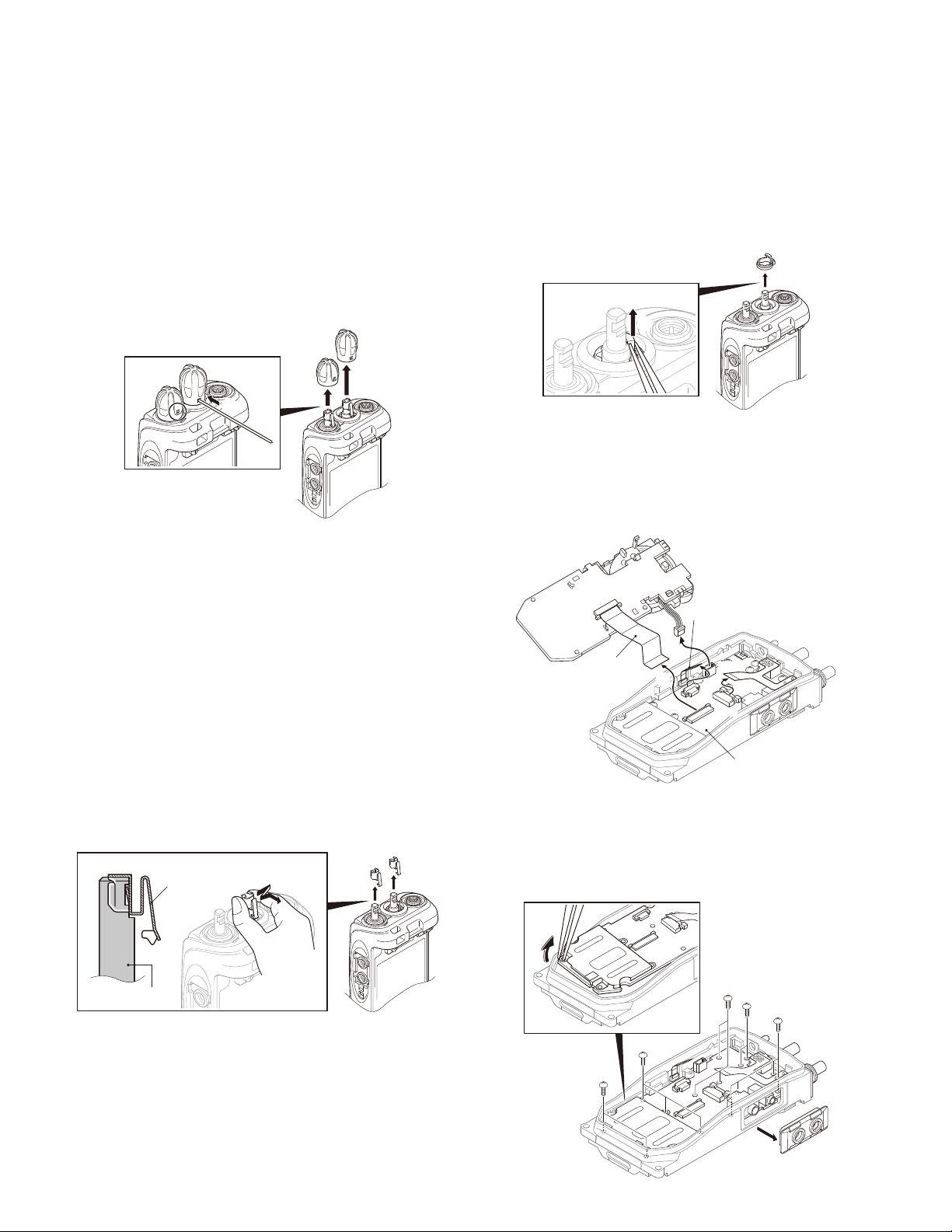
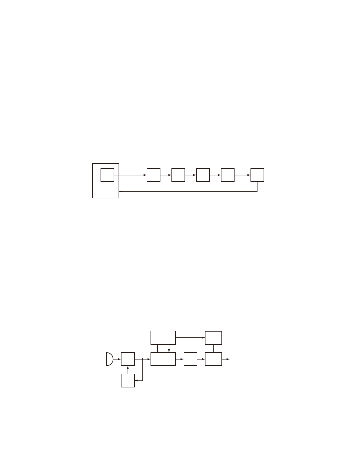
1. Precautions for Disassembly
Removing the selector knob and volume knob
■
1. Using a thin tool, insert it in the hole on the selector knob
side and push the knob spring.
Note: When you push the knob spring, take care not to
damage the resin of the knob.
2. Lift and remove the selector knob w while pushing the
knob spring.
3. Repeat steps 1 and 2 for the volume knob, to remove the
volume knob e.
:
Note:
Perform the following procedures when installing the selector knob and volume knob.
1) Match the direction for the hole of the knob and the knob
spring.
2) Push the knob onto the knob spring until a click sounds.
q
@
.
Removing the mechanical stopper (without LCD
■
models only)
1. Pick up and lift the tab of a mechanical stopper using a
pair of tweezers.
Note: Take care not to damage the packing.
2. Remove the mechanical stopper w.
Removing the TX-RX unit from the chassis
■
1. Remove the fl at cable from the connector (CN2).
2. Remove the Speaker lead wire from the connector (CN4).
w
3. Remove the PTT FPC from the connector (CN3).
4. Remove the VOL/SEL FPC from the connector (CN1).
q
@
:
q
e
r
PTT FPC
Removing the selector knob spring and volume
■
knob spring
1. Lightly grasp the left and right sides of the selector knob
spring, then shift the knob spring to the left and right,
little by little, as shown in the fi gure.
Note: Do not grasp the knob spring tightly.
2. Remove the selector knob spring w.
Note: Do not bring your fi ngers into contact with the fl at
spring of the knob spring as much as possible.
3. Repeat steps 1 and 2 for the volume knob spring, to remove the volume knob spring e.
Knob spring
Encoder
Note:
Perform the following procedures when installing the selector knob spring and volume knob spring.
1) Match the direction for the knob spring and the encoder.
2) Insert the encoder onto the knob spring until a click
sounds.
q
@
.
:
@
Flat cable
:
5. Remove the packing t from the SP/MIC jack.
6. Remove the 14 screws y.
7. Anchor the screw hole of the TX-RX unit using the tip of a
pair of tweezers as shown in the fi gure. Then lift the TXRX unit to remove it from the chassis.
>
B
B
CN3
CN2
.
CN4
;
CN1
TX-RX unit
u
B
B
B
=
8
DISASSEMBLY FOR REPAIR
Removing the speaker holder
■
There is a space of approximately 1mm (0.04 inch) be-
tween the center part of the front glass of the speaker
holder and the surface of the Display unit. Set your fi nger
on the space in the center part of the front glass, then lift
and remove it.
Speaker holder
Display unit
Removing the TOP packing
■
1. Pull the TOP packing to the left to remove the packing
that is fi t into the left groove of the chassis.
2. Pull the TOP packing to the right to remove the packing
that is fi t into the right groove of the chassis.
3. Pull the TOP packing to the center to remove the packing
that is fi t into the center groove of the chassis.
4. Remove the TOP packing.
Note:
Remove the packing slowly, as the packing of the selec-
tor part might overset when the TOP packing is removed.
If the packing is turned over, return it to the normal position using a soft tipped item (e.g., your fi nger).
;
r
q
w
e
NX-320
2. Precautions for Reassembly
Apply the bond to the inside of the selector
■
circle nut and volume circle nut
Apply the bond (W05-0019-00) or “THREE BOND 1401B”
at two points inside of the circle nut before tightening the
circle nut.
Circle nut
Mounting the chassis onto the case
■
1. Place the key top on the chassis. Then, fit the chassis
tightly into the groove of the key top.
Note:
Confi rm that the entire groove of the key top fi ts to the
chassis tightly.
2. Mount the chassis onto the case.
Note:
• After mounting the chassis onto the case, if the 16-
key part on the key top gets stuck inside the case as
shown in the fi gure, return it to the normal position using a soft tipped item (e.g., your fi nger).
Prying it with a pointed metal tool such as forceps,
may damage the key top or packing.
• Confi rm that the TOP packing is not caught in the An-
tenna or Volume holes of the case.
q
w
e
16-key part
@
.
:
@
.
:
Volume of TOP packing
Antenna of TOP packing
9
NX-320
DISASSEMBLY FOR REPAIR
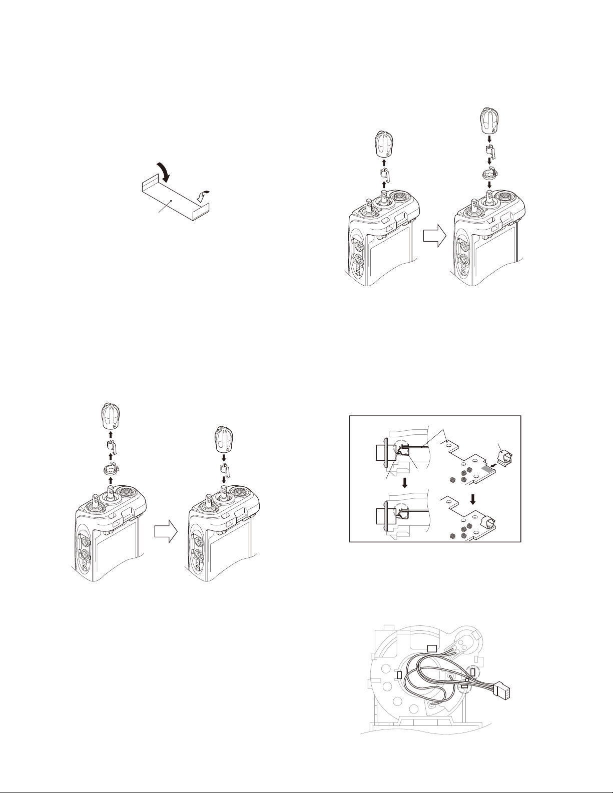
Forming the fl at cable
■
Form the right and left end of the fl at cable as shown in
the fi gure. (Bend the terminal surface of the fl at cable on
the inside.)
Note: When bending the flat cable, bend it squarely.
There is a possibility of disconnecting when the fl at cable
is bent too much.
Flat cable
Changing the channel selector from 16-channel
■
operation to free (without LCD models only)
1. Remove the channel selector knob q. (Refer to page 8
for how to remove the channel selector knob.)
2. Remove the knob spring w. (Refer to page 8 for how to
remove the knob spring.)
3. Remove the mechanical stopper e. (Refer to page 8 for
how to remove the mechanical stopper.)
4. Reassemble the channel selector knob and knob spring
that were removed in steps 1 and 2, in their original positions.
Note: Refer to page 8 for how to install the channel se-
lector knob and knob spring.
:
Note: Refer to page 8 for how to install the channel se-
lector knob and knob spring.
:
@
Connection place of the antenna hot pin and
■
.
antenna terminal
An antenna hot pin is connected with the antenna termi-
nal at the position shown in the fi gure.
Confi rm that the antenna hot pin has fi rmly come in con-
tact with the terminal when the TX-RX unit is tightened
with the screw.
Additionally, refer to the following fi gures for the connec-
tion place of the antenna terminal and the TX-RX unit.
@
.
Changing the channel selector from free opera-
■
tion to 16-channel (with LCD models only)
1. Remove the channel selector knob q. (Refer to page 8
for how to remove the channel selector knob.)
2. Remove the knob spring w. (Refer to page 8 for how to
remove the knob spring.)
3. Pinch the supplied mechanical stopper e using your fi ngers, then install it into the groove of the selector part on
the case.
4. Reassemble the channel selector knob and knob spring
that were removed in steps 1 and 2, in their original positions.
TX-RX unit
Antenna
hot pin
Align the SP/MIC lead wire
■
Align the SP/MIC lead wire as shown in the fi gure. It is
possible to fi x temporarily by interweaving the two lead
wires between the tabs (tab A and tab B) and boss of the
speaker holder.
Antenna
terminal
Antenna
terminal
B
A
10
NX-320
DISASSEMBLY FOR REPAIR
Assembly information (Sheet/Cushion)
■
When “Main Parts” is changed (ordered), “Assembled Sheet/Cushion” should also be changed (ordered) together.
The Sticker and Sheet etc are non-reusable parts. It requires the new one to get the radio’s performance after repairs.
For example, when “Plastic Cabinet Assy (A02-4130-03 (without key)/A02-4131-03 (4-key)/A02-4132-03 (16-key))” is changed,
“Sticker (B42-7417-04)” and “Fibrous Sheet (G10-1827-04)” should be ordered and changed together because Sticker (B427417-04) and Fibrous Sheet (G10-1827-04) are non-reusable.
Main Parts Assembled Sheet/ Cushion
Part Name Part Number Part Name Part Number Remark
Plastic Cabinet Assy (without key) A02-4130-03
Plastic Cabinet Assy (4-key) A02-4131-03
Plastic Cabinet Assy (16-key) A02-4132-03
Speaker T07-0787-05
Chassis A10-4148-01
MIC Element T91-0673-05 Sheet (ECM) G11-4558-04
Sticker B42-7417-04 “NEXEDGE” is printed.
Fibrous Sheet (SP) G10-1827-04
Rubber Cushion (SP) G11-4272-14
Sheet (SP) G11-4527-04
Sheet (PTT) G11-4543-04
Rubber Sheet (FET) G11-4315-14
Sheet (Air) G11-4500-04
Used for stabilizing the radiation performance
of the FET.
This sheet is put on the air vent hole.
This sheet lets air through, but does not let
water through.
11
NX-320
CIRCUIT DESCRIPTION
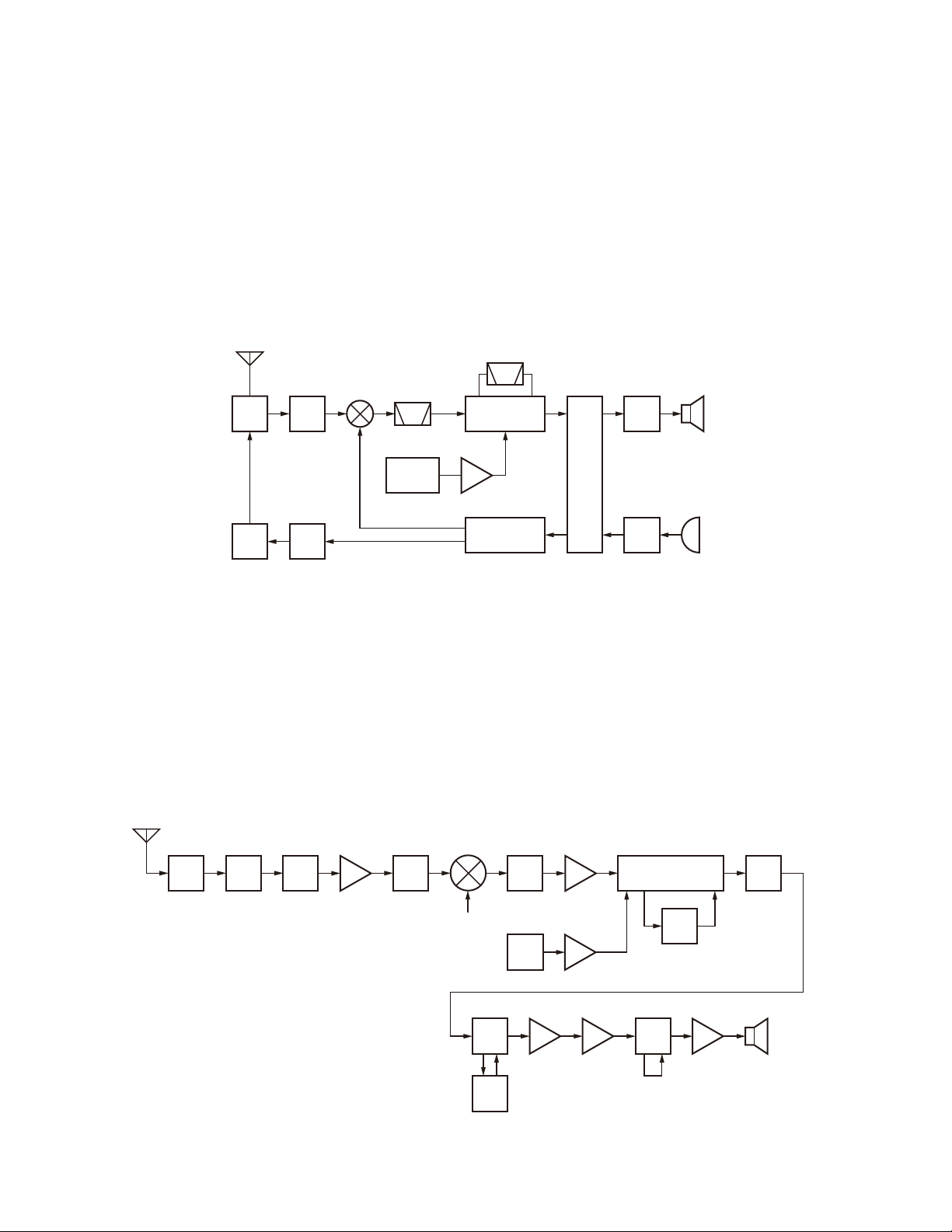
1. Overview
The NX-320 is a UHF portable transceiver designed to
operate in the frequency range of 450 to 520MHz (K,K2,K3)
or 400 to 470MHz (K4,K5,K6,E,E2,E3). The unit consists of a
receiver, transmitter, phase-locked loop (PLL) frequency synthesizer, baseband parts, power supply, and control circuits.
ANT
ANT
SW
PA
AMPTXAMP
:@
400~470MHz (K4,K5,K6,E,E2,E3)
450~520MHz (K,K2,K3)
TX/RX:
AMP
RF
:
1st MIX
MCF
49.95MHz
16.8MHz
TCXO
@
:
2. Frequency Confi guration
The receiver is a double-conversion superheterodyne
using the first intermediate frequency (IF) of 49.95MHz
and the second IF of 450kHz. Incoming signals from the
antenna are mixed with the local signal from the PLL circuit
to produce the fi rst IF of 49.95MHz. This is then mixed with
the 50.4MHz second local oscillator output to produce the
450kHz second IF. The transmit signal frequency is generated by the PLL VCO, and modulated by the signal from the
DSP. It is then amplifi ed and fed to the antenna.
CF
450kHz
SP
MIX
IF AMP
x3
50.4MHz
PLL
VCO
350.05~420.05MHz (K4,K5,K6,E,E2,E3)
400.05~470.05MHz (K,K2,K3)
AF
AMP
Baseband Circuit
MIC
AMP
MIC
Fig. 1 Frequency confi guration
3. Receiver System
3-1. RF circuit
An incoming RF signal from the antenna terminal is
passed through the antenna switch (D102, D103, D105 and
D106) and then the band-pass fi lter (L212, L213 and L214).
The band-pass fi lter is adjusted by a variable capacitor. The
input voltage to the variable capacitor is regulated by the
ANT
LPF
L114
L115
L116
D102,D103
D105,D106
ANT
SW
Q202 XF1
BPF
L212
RF AMP MCF
L213
L214
BPF BPF
L209
L208
L207
OSC (PLL)
voltage output from the D/A converter (IC4). The signal is
amplifi ed by an RF amplifi er (Q202), and passed through the
band-pass fi lter (L207, L208 and L209). The resulting signal
is applied to the fi rst mixer (Q201), where it is mixed with
the first local oscillator signal output from the frequency
synthesizer to produce the fi rst IF (49.95MHz).
Q201
1st MIX
1st PLL
IC610
ASIC
X401
TCXO
16.8MHz
IC904
Q303
IF AMP
Q301
x3
IC2 (1/2)
2nd OSC
IC302
MIX, AGC
BPF
CF1
IC4
VOL
IC901
CF2
BPF
SP
12
DSP
IC603
Fig. 2 RF and IF circuit
CIRCUIT DESCRIPTION
NX-320
3-2. IF circuit
The fi rst IF signal is passed through a four-pole monolithic
crystal fi lter (XF1) to reject adjacent channel signals. The fi ltered fi rst IF signal is amplifi ed by the fi rst IF amplifi er (Q303)
and then applied to the IF system IC (IC302). The IF system
IC provides a second mixer, AGC amplifi er, and RSSI (Received Signal Strength Indicator).
The second mixer mixes the first IF signal with the
50.4MHz of the second local oscillator output and produces
the second IF signal of 450kHz.
The second IF signal is passed through the ceramic fi lter
(CF1) to reject the adjacent channel signal. The fi ltered second IF signal is amplifi ed by the AGC amplifi er.
The signal from the AGC amplifier is input to the ASIC
(IC610) through the ceramic fi lter (CF2).
DET
IC610
ASQAPC
ASQDET
IC1 (1/2)
LPF
IC1 (2/2)
Fig. 3 Squelch circuit
3-3. Audio amplifi er circuit
Audio processing (high-pass filter, low-pass filter, deemphasized and so on) at FM mode and decoding at NXDN
mode are processed by the DSP. The audio signal from
IC610 and IC603 goes through the amplifier (IC904). The
signal then goes through an electronic volume control (IC4),
and AF amplifi er (IC901).
While AFSW is High, the power supply of audio power
amplifi er (IC901) is activated, and the output to the speaker
turns ON.
3-4. Squelch circuit
It amplifi es the demodulated noise signal from IC610 after fi ltering through the LPF and HPF circuit. The amplifi ed
signal is then converted to a DC signal by the detection circuit. The converted signal is fed back to IC610.
HPF
Q3
AMP
D2
RECT
ASQ
IC304 (1/2)
AMP
4. Transmitter System
4-1. Audio band circuit
The signal from the microphone is amplifi ed by IC2 (2/2)
and limited by the AGC circuit which is composed of D3,
D4, Q4 and Q5. IC2 works as an anti-aliasing LPF fi lter.
4-2. Baseband circuit
The audio signal output from the baseband circuit is converted to digital data with a sampling frequency of 48kHz.
This digital data is sent to the DSP (IC603), and voice signals
of 300Hz or lower and frequencies of 3kHz or higher are cut
IC603
DSP
IC2 (2/2)
MIC
AMP
AGC
D3,D4
Q4,Q5
Fig. 4 Audio band and Baseband circuit
IC610
off and the audio range of 300Hz to 3kHz is extracted. The
audio signal is then pre-emphasized in FM mode and synthesized with the signals, such as QT and DQT, as required,
and is then output from IC610. In Digital mode, the audio
signal is converted to the 4-Level FSK baseband signal and
output from IC610. The DTMF and MSK baseband signals
are also generated by the DSP and output by IC610
The LPF (IC6) works as a smoothing fi lter. The level output according to the transmit carrier is fi ne-adjusted according to each modulation method.
IC403
PLL IC
IC6 (1/2)
LPF VCO to TX stage
13
NX-320
CIRCUIT DESCRIPTION
4-3. VOX
The DSP detects the audio level. If the detected level be-
comes higher than the threshold level, the VOX starts.
4-4. Drive and Final amplifi er
The signal from the T/R switch (D413 is on) is amplifi ed
by the pre-drive amplifier (Q102) to 16~17dBm. It makes
it possible to spoil input to the drive amplifier by controlling the power supply of the pre-drive amplifier with the
PD switch (Q110). The output of the pre-drive amplifi er is
amplifi ed by the drive and fi nal amplifi ers (Q103, Q104) to
5.0W (1.0W when the power is low). Q103 and Q104 are
MOS FETs. The output of the fi nal amplifi er is then passed
through the harmonic fi lter (LPF) and antenna switch (D102,
D103 are on) and applied to the antenna terminal.
Q102 Q103
T/R SW (D413)
from
VCC for Pre-Drive AMP
from PD SW (Q110)
+B
Pre-Drive
AMP
R153
R154
R155
4-5. APC circuit
The APC circuit always monitors the current flowing
through the RF power amplifi er (Q104) and keeps a constant
current. The voltage drop at R153, R154 and R155 is caused
by the current fl owing through the RF power amplifi er and
this voltage is applied to the differential amplifier (IC101
1/2). IC101 (2/2) compares the output voltage of IC101 (1/2)
with the reference voltage from IC610, and the output of
IC101 (2/2) controls the VGG of Q103 and Q104 to make the
both current constant. The change of power high/low is carried out by the change of the reference voltage. Q106, Q107
and Q108 are turned on and Q105 and Q109 are turned off
during transmission and the APC circuit is active.
ANT
Q104
D102,D103
Drive
AMP
Final
AMP
ANT
SW
VGG
LPF
Reference voltage
from IC610
Fig. 5 Drive and fi nal amplifi er and APC circuit
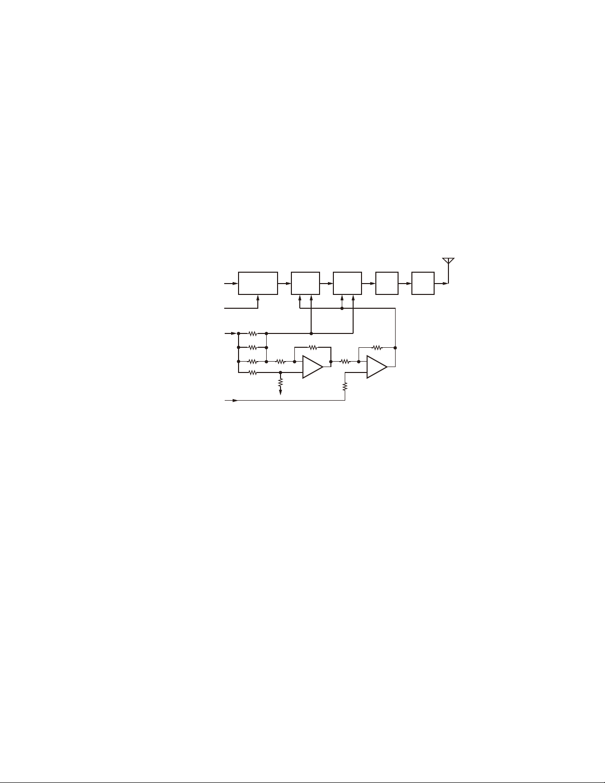
5. PLL Frequency Synthesizer
5-1. TCXO (X401)
The TCXO (X401) generates a reference frequency of
16.8MHz for the PLL frequency synthesizer. This reference
frequency is applied to pin 9 of the PLL IC (IC403) and is
connected to the IF circuit as a 2nd local signal through the
Tripler (Q301).
The frequency adjustment is achieved by switching the
ratio of dividing frequency. The resolution of the adjusting
frequency is approximately 4Hz.
5-2. VCO
There is a RX VCO and a TX VCO.
The TX VCO (Q402) generates a transmit carrier and the
RX VCO (Q401) generates a 1st local signal. For the VCO
oscillation frequency, the transmit carrier is 450 to 520MHz
(K,K2,K3) or 400 to 470MHz (K4,K5,K6,E,E2,E3) and the 1st
local receive signal is 400.05 to 470.05MHz (K,K2,K3) or
350.05 to 420.05MHz (K4,K5,K6,E,E2,E3).
The VCO oscillation frequency is determined by one system of operation switching terminal “T/R” and two systems
of voltage control terminals “CV” and “ASSIST”.
IC101
(1/2)
The operation switching terminal, “T/R”, is controlled by
the control line (/T_R) output from the ASIC (IC610). When
the /T_R logic is low, the VCO outputs the transmit carrier
and when it is high, it outputs a 1st local receive signal.
The voltage control terminals, “CV” and “ASSIST”, are
controlled by the PLL IC (IC403) and ASIC (IC610) and the
output frequency changes continuously according to the
applied voltage. For the modulation input terminal, “VCO_
MOD”, the output frequency changes according to the
applied voltage. This is used to modulate the VCO output.
“VCO_MOD” works only when “/T_R” is low.
IC101
(2/2)
5-3. PLL IC (IC403)
The PLL IC compares the differences in phases of the
VCO oscillation frequency and the TCXO reference frequency, returns the difference to the VCO CV terminal and realizes the “Phase Locked Loop” for the return control. This
allows the VCO oscillation frequency to accurately match
(lock) the desired frequency.
14
CIRCUIT DESCRIPTION
NX-320
When the frequency is controlled by the PLL, the frequency convergence time increases as the frequency difference increases when the set frequency is changed. To supplement this, the ASIC is used before control by the PLL IC
to bring the VCO oscillation frequency close to the desired
frequency. As a result, the VCO CV voltage does not change
and is always stable at approximately 2.5V.
The desired frequency is set for the PLL IC by the ASIC
(IC610) through the 3-line “SDO1”, “PCK_RF”, “/PCS_RF”
serial bus. Whether the PLL IC is locked or not is monitored
by the ASIC through the “PLD” signal line. If the VCO is not
the desired frequency (unlocked), the “PLD” logic is low.
The modulation signal of the Low-speed data is applied to
pin 23 of the PLL IC (IC403).
X401
16.8MHz
TCXO
SDO1
PCK_RF
/PCS_RF
PLLMOD
IC403 Q405
Loop
Filter
PLL
IC404 (1/2)
CV
VCO MOD
IC402
ASSIST
100C
Q401,Q402
D402~D411
D415
VCO
The modulation signal is digital data of a sampling frequency of 96kHz set for the PLL IC by the DSP (IC603)
through the “PLLMOD” line.
5-4. Local switch (D412, D413)
The connection destination of the signal output from the
buffer amplifier (Q408) is changed with the diode switch
(D413) that is controlled by the transmission power supply,
50T, and the diode switch (D412) that is controlled by the
receive power supply, 50R. If the 50T logic is high, it is connected to a send-side pre-drive (Q102). If the 50T logic is
low, it is connected to a receive-side mixer (Q201).
BUFF
AMP
Q408
BUFF
AMP
50CS
LPF
D412,D413
T/R
SW
50T
50R
to TX stage
to 1st Mixer
Fig. 6 PLL block diagram
6. Control Circuit
The control circuit consists of the ASIC (IC610) and its pe-
ripheral circuits. IC610 mainly performs the following:
1) Switching between transmission and reception by PTT
signal input.
2) Reading system, zone, frequency, and program data from
the memory circuit.
3) Sending frequency program data to the PLL.
4) Controlling squelch on/off by the DC voltage from the
squelch circuit.
5) Controlling the audio mute circuit by decode data input.
6-1. ASIC
The ASIC (IC610) is a 32-bit RISC processor, equipped
with peripheral function and ADC/DAC.
This ASIC operates at 18.432MHz clock and 3.3V/1.5V
DC. It controls the fl ash memory, SRAM, DSP, the receive
circuit, the transmitter circuit, the control circuit, and the display circuit and transfers data to or from an external device.
6-2. Memory circuit
The memory circuit consists of the ASIC (IC610), the
SRAM (IC605), and the flash memory (IC601). The flash
memory has a capacity of 32M-bit that contains the transceiver control program for the ASIC and stores the data. It
also stores the data for transceiver channels and operating
parameters that are written by the FPU. This program can
be easily written from external devices. The SRAM has a
capacity of 1M-bit that contains work area and data area.
Flash memory
■
Note: The fl ash memory stores the data that is written by
the FPU (KPG-141D), tuning data (Deviation, Squelch, etc.),
and firmware program (User mode, Test mode, Tuning
mode, etc.).
SRAM (Static memory)
■
Note: The SRAM has a temporary data area and work area.
15
NX-320
CIRCUIT DESCRIPTION
6-3. LCD
The LCD is controlled using the 4 serial lines (SDI0, /
LCDCS, SCK0, SDO0) from the ASIC (IC610).
6-4. Key detection circuit
Keys are detected using the LCD controller driver IC (IC8).
If a pressed key is detected by IC8, it is informed to IC610
through the serial line.
6-5. Low battery warning
The battery voltage is divided using R514 and R515 and
is detected by the ASIC (IC610). When the battery voltage
falls below the voltage set by the Low battery warning adjustment, the red LED blinks to notify the operator that it is
time to replace the battery. If the battery voltage falls even
more (approx. 5.8V), a beep sounds and transmission stops.
Low battery warning Battery condition
The red LED blinks during
transmission.
The red LED blinks and the
warning tone beeps while the
PTT switch is pressed.
The battery voltage is low but
the transceiver is still usable.
The battery voltage is low and
the transceiver is not usable to
make calls.
6-6. DSP
The DSP circuit consists of a DSP (IC603) and processes
the baseband signal. The DSP operates on an external clock
of 18.432MHz (the same as the IC610), the I/O section operates at 3.3V and the core section operates at 1.5V. The
DSP carries out the following processes:
• 4 Level FSK processing
• Analog FM pre-emphasis/de-emphasis
• Vocoder processing between audio codec and modula-
tion/demodulation
• CAI processing, such as error correction encoding
• QT/DQT encoding/decoding
• LTR encoding/decoding
• DTMF encoding/decoding
• MSK encoding/decoding
• 2-tone encoding/decoding
• 5-tone encoding/decoding
• Compressor/expander processing
• Voice scrambler processing
• Transmit/receive audio fi ltering processing
• Microphone amplifi er AGC processing
• Audio mute processing
• Modulation level processing
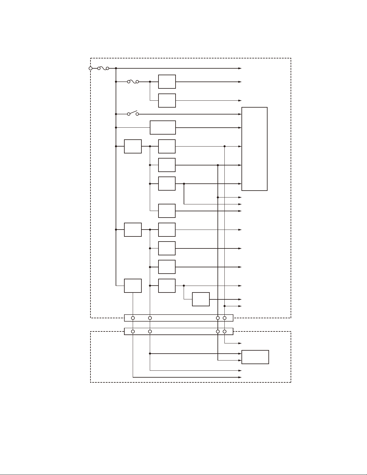
7. Power Supply Circuit
The battery voltage (+B) is provided from the battery
terminal on the TX-RX unit (X57). The battery voltage passes
through the 2.5A fuse (F1), and goes to the RF fi nal amplifi er, AVR ICs (IC504, IC902), DC/DC converter (IC506), and
voltage detector IC (IC507). The voltage detector watches
the battery voltage. If the battery voltage is 5.6V or higher,
the detector outputs High.
When the VOL SW is turned on, SB1 becomes high (battery voltage). DC/DC (IC506) operates if both SB1 and the
output of the detector are high. IC506 outputs 3.8V and
activates IC502 (33M), IC503 (15M), IC501 (33A) and IC505
(33C). As a result, the ASIC and DSP operate.
The SBC signal becomes High after the ASIC operates,
IC504 (50C), IC902 (50V) and Q501 (SB2) are turned on.
When the /SAVE signal becomes High, Q512 (50C) operates. Switches (Q503, Q505) are controlled by the ASIC.
Q505 (50T) is turned on in transmit mode. Q503 (50R) is
turned on in receive mode.
When the VOL SW is turned off, the /PSW signal becomes Low. After detecting the /PSW signal, the ASIC
changes the SBC signal to Low.
50C is fed to IC509 (100C). IC509, D511 and D512 consist of a voltage doubler. C543 is charged to 5V by 50C and
switched to C545 by the “DDCLK” control signal. The 100C
circuit then outputs approximately +10VDC.
8. Signaling Circuit
8-1.
Encode (QT/DQT/LTR/DTMF/2-tone/5-tone/MSK)
Each signaling data signal of QT, DQT, LTR, DTMF,
2-tone/5-tone and MSK is generated by the DSP circuit, superimposed on a modulation signal and output from IC610.
Each deviation of the TX QT, DQT, LTR, DTMF, 2-tone/5-tone
and MSK tone is adjusted by changing the output level of
IC603 and the resulting signal is routed to the VCO and PLL.
8-2.
Decode (QT/DQT/LTR/DTMF/2-tone/5-tone/MSK)
The audio signal is removed from the FM detection signal
sent to the DSP circuit and the resulting signal is decoded.
9. Compander Circuit
The term “compander” means compressor and expander. The compander reduces noise by utilizing a compressor
and an expander. The transceiver contains a DSP (IC603) to
perform this operation. The transceiver compander can be
turned on or off using the FPU.
16
TX-RX unit
+B
F1
2.5A
CIRCUIT DESCRIPTION
F2
1.0A
Q902
SW
NX-320
Final AMP, APC
AFPA
VOL/SW
IC506
38M
IC504
50C
IC902
50V
IC507
5.6V Det
IC501
33A
IC502
33M
IC503
15M
IC505
33C
IC509
100C
Q505
50T
Q503
50R
2-pin Jack
/PSW
/BINT
ASIC
IC610
DSP, FLASH, SRAM
DSP
PLL, TCXO
ASSIST
TX circuit
RX circuit
Display unit
CN2
CN5
Q501
SB2
Q512
50CS
Ripple
filter
Fig. 7 Power supply circuit
PLL, fin
VCO
AF circuit
AF circuit, DAC
IC8
LCD driver
SQL circuit
LED
17
NX-320
COMPONENTS DESCRIPTION
Display unit (X54-3760-XX)
Ref. No. Part Name Description
IC1 IC ASQ BPF
IC2 IC AF LPF/MIC amplifi er
IC4 IC D/A converter
IC6 IC VCO MOD/VREF
IC8 IC LCD driver
Q1 Transistor TX/BUSY LED switch
Q2 FET SQL noise BW switch
Q3 Transistor SQL noise amplifi er
Q4,5 Transistor MIC AGC
Q6 Transistor KEY backlight switch
Q7 Transistor KEY backlight switch control
Q8 Transistor LCD backlight switch
D1 LED TX/BUSY LED
D2 Diode Noise detector
D3,4 Diode AGC detector
D7~14 LED KEY backlight
D15,16 Diode KEY control
D18,19 LED LCD backlight
TX-RX unit (X57-8050-XX)
Ref. No. Part Name Description
IC101 IC OP AMP (APC)
IC201 IC DC amplifi er (BPF)
IC302 IC FM system
IC304 IC DC amplifi er (RSSI/ASQL)
IC402 IC DC amplifi er (Assist)
IC403 IC PLL system
IC404 IC DC amplifi er (CV/APC)
IC501 IC Voltage regulator (33A)
IC502 IC Voltage regulator (33M)
IC503 IC DC/DC converter (15M)
IC504 IC Voltage regulator (50C)
IC505 IC Voltage regulator (33C)
IC506 IC DC/DC converter (38M)
IC507 IC Voltage detector (BATT)
IC509 IC DC/DC converter (100C)
IC601 IC Flash memory
IC603 IC DSP
IC605 IC SRAM
IC607 IC Voltage detector (Reset)
Ref. No. Part Name Description
IC609 IC Buffer (Clock)
IC610 IC ASIC
IC611,612 IC AND gate (2 input)
IC613 IC Motion sensor
IC901 IC AF power amplifi er
IC902 IC Voltage regulator (50V)
IC904 IC OP AMP (Beep/voice/RX AF)
Q102 Transistor Pre-drive amplifi er
Q103 FET Drive amplifi er
Q104 FET RF fi nal amplifi er
Q105~109 Transistor APC switch
Q110 FET PD switch
Q201 FET 1st mixer
Q202 FET RF AMP (RX)
Q301 Transistor Tripler (2nd local)
Q303 Transistor IF amplifi er
Q401 FET RX VCO
Q402 FET TX VCO
Q403 Transistor Ripple fi lter
Q405 Transistor Buffer amplifi er
Q406,407 FET T/R VCO switch
Q408 Transistor Buffer amplifi er
Q501 FET DC switch (SB2)
Q502 FET DC switch control (SB2)
Q503 Transistor DC switch (50R)
Q505 Transistor DC switch (50T)
Q506,507 FET Level converter
Q509 Transistor DC/DC control (100C)
Q510 Transistor DC/DC control (38M)
Q511 Transistor DC switch control (50T)
Q512 FET DC switch (50CS)
Q602 FET DC switch (System)
Q901 Transistor DC switch (AF mute)
Q902 Transistor DC switch (AF PA amplifi er)
Q903 Transistor DC switch (AF mute)
Q904,905 FET AF power mute
Q906 Transistor EXT/MIC switch
Q907 FET Level converter
D101 Zener diode APC protect
D102,103 Diode Antenna switch
D105,106 Diode Antenna switch
18
COMPONENTS DESCRIPTION
NX-320
Ref. No. Part Name Description
D201~204
D206,207
D401 Diode Bypass
D402
D403
D404
D405~409
D410
D411
Variable capacitance diode
Variable capacitance diode
Variable capacitance diode
Variable capacitance diode
Variable capacitance diode
Variable capacitance diode
Variable capacitance diode
Variable capacitance diode
BPF tune
BPF tune
Assist tune
TX VCO tune
RX VCO tune
Assist tune
TX modulation
Assist tune
Ref. No. Part Name Description
D412,413 Diode T/R switch
D414 Diode Speed up
D415
D501 Diode Reverse protection
D502 Diode Speed up
D505,506 Diode DC/DC converter
D508 Diode DC/DC converter
D509 Diode Reverse current protection
D511,512 Diode DC/DC converter
D901 Diode Reverse current protection
D902 Diode 50V switch control
Variable capacitance diode
Assist tune
19
NX-320
PARTS LIST
New Parts.
✽
Parts without Parts No. are not supplied.
Les articles non mentionnes dans le Parts No. ne sont pas fournis.
Teile ohne Parts No. werden nicht geliefert.
NX-320
DISPLAY UNIT (X54-3760-XX)
Ref. No.
indicates safety critical components.
New
Ad dress
parts
Parts No. Description
Destination
NX-320
1 2B ✽ A02-4130-03 PLASTIC CABINET ASSY K,K4,E3
2 2B ✽ A02-4131-03 PLASTIC CABINET ASSY (4KEY) K2,K5,E2
3 1B ✽ A02-4132-03 PLASTIC CABINET ASSY (16KEY) K3,K6,E
4 3A ✽ A10-4148-01 CHASSIS
6 3A B01-0694-13 ESCUTCHEON
7 1C B09-0686-03 CAP ACCESSORY
8 3B B11-1869-04 ILLUMINATION GUIDE (TX/BUSY)
9 1A ✽ B11-1890-04 FILTER (LCD) K2,K3,K5
9 1A ✽ B11-1890-04 FILTER (LCD) K6,E,E2
10 1A ✽ B11-1891-02 ILLUMINATION GUIDE (LCD) K2,K3,K5
10 1A ✽ B11-1891-02 ILLUMINATION GUIDE (LCD) K6,E,E2
11 1A B38-0935-05 LCD K2,K3,K5
11 1A B38-0935-05 LCD K6,E,E2
12 1A B42-7417-04 STICKER
13 2D ✽ B62-2292-00 INSTRUCTION MANUAL (K TYPE) K,K2,K3
13 2D ✽ B62-2292-00 INSTRUCTION MANUAL (K TYPE) K4,K5,K6
14 2D ✽ B62-2319-00 INSTRUCTION MANUAL (E TYPE) E,E2,E3
16 1B,1D ✽ D32-0454-04 STOPPER (16CH)
18 3A E04-0467-15 RF COAXIAL RECEPTACLE (SMA)
19 2A ✽ E23-1363-04 TERMINAL (ANT)
20 1A ✽ E29-1232-05 INTER CONNECTOR (LCD) K2,K3,K5
20 1A ✽ E29-1232-05 INTER CONNECTOR (LCD) K6,E,E2
21 1A ✽ E37-1532-05
22 2A ✽ E37-1537-05 FLAT CABLE (TXRX-DISPLAY)
23 3A ✽ E72-0435-03 TERMINAL BLOCK
25 2A ✽ F10-3149-03 SHIELDING COVER
26 1A ✽ G02-1864-04 EARTH SPRING (DISPLAY PCB)
27 1B ✽ G09-0443-04 KNOB SPRING (VOL/SELECTOR)
28 1B ✽ G10-1827-04 FIBROUS SHEET (SP)
29 1A G11-4272-14 RUBBER CUSHION (SP)
30 3A G11-4315-14 SHEET (FET)
31 1A G11-4335-14 SHEET (LCD) K2,K3,K5
31 1A G11-4335-14 SHEET (LCD) K6,E,E2
32 3A G11-4368-04 SHEET (TERMINAL BLOCK)
33 3A G11-4500-04 SHEET (AIR)
34 1A G11-4527-04 SHEET (SP)
35 3A ✽ G11-4543-04 SHEET (PTT)
36 1A ✽ G11-4558-04 SHEET (ECM)
37 3A ✽ G11-4561-04 SHEET (CHASSIS:TX/BUSY)
38 1A ✽ G11-4562-04 SHEET (SP HOLDER)
39 2A G13-2220-04 CUSHION (DISPLAY PCB)
40 3A G53-1603-04 PACKING (SMA)
41 3A G53-1832-03 PACKING (JACK)
42 2B ✽ G53-1862-02 PACKING (TOP)
43 2B ✽ G53-1863-01 PACKING K,K4,E3
44 2B ✽ G53-1864-01 PACKING (4KEY) K2,K5,E2
45 1B ✽ G53-1865-01 PACKING (16KEY) K3,K6,E
46 1A,3A ✽ G53-1866-04 PACKING (TERMINAL,ECM)
47 1C ✽ H12-4312-02 PACKING FIXTURE
48 3C ✽ H52-2454-02 ITEM CARTON CASE K,K2,K3
48 3C ✽ H52-2454-02 ITEM CARTON CASE K4,K5,K6
LEAD WIRE WITH CONNECTOR (SP/ECM)
L : Scandinavia K : USA P : Canada
Y : PX (Far East, Hawaii) T : England E : Eu rope
C : China X : Australia M : Oth er Areas
Ref. No.
49 1D J19-5483-23 HOLDER ACCESSORY
50 1A ✽ J19-5547-01 HOLDER (FG-SP)
51 1A ✽ J21-8631-03 MOUNTING HARDWARE (LCD) K2,K3,K5
51 1A ✽ J21-8631-03 MOUNTING HARDWARE (LCD) K6,E,E2
52 1D J29-0701-15 BELT CLIP ACCESSORY
53 3A J87-0027-05 FPC (LEAD FREE) (PTT)
54 2A ✽ J87-0040-05 FPC (LEAD FREE) (VOL/SELECTOR)
56 1A ✽ K29-9500-03 KNOB (PTT)
57 1B ✽ K29-9501-03 BUTTON KNOB (SIDE1/SIDE2/AUX)
58 1B ✽ K29-9485-03 KNOB (VOL)
59 1B ✽ K29-9486-03 KNOB (SELECTOR)
A 3A N09-2438-05 BINDING HEAD SCREW (ANT)
B 3A ✽ N09-6608-05 SPECIAL SCREW (CASE)
C 3A ✽ N14-0864-04 CIRCULAR NUT (VOL)
D 3A ✽ N14-0865-04 CIRCULAR NUT (SELECTOR)
E 3A N30-3006-43 PAN HEAD MACHINE SCREW (ESCUT)
F
VR1 3A ✽ R31-0685-05 VARIABLE RESISTOR (VOL)
S101 3A ✽ S60-0448-05 ROTARY SWITCH (SELECTOR)
65 1A T07-0787-05 SPEAKER
- ✽ X57-8050-12 SERVICE TX-RX UNIT K,K2,K3
- ✽ X57-8050-13 SERVICE TX-RX UNIT K4,K5,K6
- ✽ X57-8050-13 SERVICE TX-RX UNIT E,E2,E3
New
Ad dress
parts
1A,2A,3A
N83-2005-48 PAN HEAD TAPTITE SCREW (PCB)
Parts No. Description
Destination
DISPLAY UNIT (X54-3760-XX) -10: K3,K6,E -11: K2,K5,E2 -12: K,K4,E3
D1 B30-2278-05 LED (RED/YELLOW)
D7-14 B30-2337-05 LED (YELLOW) K3,K6,E
D13,14 B30-2337-05 LED (YELLOW) K2,K5,E2
D18,19 B30-2210-05 LED (TLY) K2,K3,K5
D18,19 B30-2210-05 LED (TLY) K6,E,E2
C1 CK73HB1H471K CHIP C 470PF K
C2 CK73HB1H681K CHIP C 680PF K
C3 CC73HCH1H270J CHIP C 27PF J
C4 CK73HB1H471K CHIP C 470PF K
C5 CK73HB1A104K CHIP C 0.10UF K
C6 CK73HB1H102K CHIP C 1000PF K
C7,8 CC73HCH1H470J CHIP C 47PF J
C10 CC73HCH1H101J CHIP C 100PF J
C11 CK73HB1H681K CHIP C 680PF K
C13 CC73HCH1H101J CHIP C 100PF J
C15 CK73HB1E103K CHIP C 0.010UF K
C16 CK73HB1H102K CHIP C 1000PF K
C19 CK73HB1A104K CHIP C 0.10UF K
C20 CK73HB1H102K CHIP C 1000PF K
C21 CK73HB1E103K CHIP C 0.010UF K
C22 CK73HB1A224K CHIP C 0.22UF K
C23 CC73HCH1H470J CHIP C 47PF J
C25 CK73HB1A224K CHIP C 0.22UF K
C26 CC73HCH1H470J CHIP C 47PF J
C28,29 CC73HCH1H470J CHIP C 47PF J
C30 CK73HB0J105K CHIP C 1.0UF K
C31 CC73HCH1H470J CHIP C 47PF J
20

Ref. No.
C32 CK73HB1H122K CHIP C 1200PF K
C33,34 CC73HCH1H470J CHIP C 47PF J
C35 CK73HB1A104K CHIP C 0.10UF K
C36 CC73HCH1H470J CHIP C 47PF J
C37 CK73HB1H472K CHIP C 4700PF K
Ad dress
New
parts
Parts No. Description
PARTS LIST
Desti-
nation
Ref. No.
CP14 RK74HA1J102J CHIP-COM 1.0K J 1/16W K6,E,E2
R1 RK73HB1J472J CHIP R 4.7K J 1/16W
R2 RK73HB1J103J CHIP R 10K J 1/16W
R3 RK73HB1J391J CHIP R 390 J 1/16W
R4 RK73HB1J823J CHIP R 82K J 1/16W
Ad dress
New
Parts No. Description
parts
NX-320
DISPLAY UNIT (X54-3760-XX)
Destination
C38 CC73HCH1H181J CHIP C 180PF J
C39 CK73HB1A104K CHIP C 0.10UF K
C40 CC73HCH1H470J CHIP C 47PF J
C42-44 CC73HCH1H470J CHIP C 47PF J
C45 CK73HB1H102K CHIP C 1000PF K
C47 CK73HB1A104K CHIP C 0.10UF K
C48 CK73HB0J105K CHIP C 1.0UF K
C49 CK73HB1H102K CHIP C 1000PF K
C52,53 CK73HB1A104K CHIP C 0.10UF K
C54 CK73HB1H331K CHIP C 330PF K
C58 CC73HCH1H680J CHIP C 68PF J
C62 CC73HCH1H101J CHIP C 100PF J
C63,64 CK73HB0J105K CHIP C 1.0UF K
C67 CK73HB1H102K CHIP C 1000PF K
C68 CK73HB1E103K CHIP C 0.010UF K
C70 CK73HB0J105K CHIP C 1.0UF K
C71 CK73HB1A104K CHIP C 0.10UF K
C73 CK73GB0J106K CHIP C 10UF K
C74 CK73HB0J105K CHIP C 1.0UF K
C78 CK73HB1E103K CHIP C 0.010UF K K2,K3,K5
C78 CK73HB1E103K CHIP C 0.010UF K K6,E,E2
C79 CK73HB1A473K CHIP C 0.047UF K K2,K3,K5
C79 CK73HB1A473K CHIP C 0.047UF K K6,E,E2
C83 CK73HB1H102K CHIP C 1000PF K K2,K3,K5
C83 CK73HB1H102K CHIP C 1000PF K K6,E,E2
C84 CK73HB1A473K CHIP C 0.047UF K K2,K3,K5
C84 CK73HB1A473K CHIP C 0.047UF K K6,E,E2
C85 CK73HB1H681K CHIP C 680PF K K2,K3,K5
C85 CK73HB1H681K CHIP C 680PF K K6,E,E2
C90 CK73HB1E103K CHIP C 0.010UF K K2,K3,K5
R5 RK73HB1J100J CHIP R 10 J 1/16W
R6 RK73HB1J821J CHIP R 820 J 1/16W
R7 RK73HB1J472J CHIP R 4.7K J 1/16W
R8 RK73HB1J153J CHIP R 15K J 1/16W
R9 RK73HB1J333J CHIP R 33K J 1/16W
R10 RK73HB1J000J CHIP R 0.0 J 1/16W
R11,12 RK73HB1J334J CHIP R 330K J 1/16W
R13 RK73HB1J471J CHIP R 470 J 1/16W
R14 RK73HB1J334J CHIP R 330K J 1/16W
R15 RK73HB1J332J CHIP R 3.3K J 1/16W
R16 RK73HB1J470J CHIP R 47 J 1/16W
R17 RK73HB1J104J CHIP R 100K J 1/16W
R18 RK73HB1J393J CHIP R 39K J 1/16W
R19,20 RK73HB1J224J CHIP R 220K J 1/16W
R21,22 RK73HB1J563J CHIP R 56K J 1/16W
R23 RK73HB1J222J CHIP R 2.2K J 1/16W
R24 RK73HB1J000J CHIP R 0.0 J 1/16W
R26 RK73HB1J683J CHIP R 68K J 1/16W
R28-30 RK73HB1J000J CHIP R 0.0 J 1/16W
R33-35 RK73HB1J104J CHIP R 100K J 1/16W
R37 RK73HB1J154J CHIP R 150K J 1/16W
R39,40 RK73HB1J103J CHIP R 10K J 1/16W
R41,42 RK73HB1J683J CHIP R 68K J 1/16W
R44,45 RK73HB1J104J CHIP R 100K J 1/16W
R47 RK73HB1J223J CHIP R 22K J 1/16W
R50 RK73HB1J223J CHIP R 22K J 1/16W
R52 RK73HB1J471J CHIP R 470 J 1/16W
R53 RK73HB1J182J CHIP R 1.8K J 1/16W
R61-64 RK73HB1J332J CHIP R 3.3K J 1/16W K3,K6,E
R64 RK73HB1J332J CHIP R 3.3K J 1/16W K2,K5,E2
C90 CK73HB1E103K CHIP C 0.010UF K K6,E,E2
C91 CK73HB1H471K CHIP C 470PF K
C92 CK73HB1H102K CHIP C 1000PF K
C93,94 CK73HB1E103K CHIP C 0.010UF K
CN5 ✽ E40-6893-05 FLAT CABLE CONNECTOR (24P)
CN6 E40-6883-05 FLAT CABLE CONNECTOR (6P)
L1,2 L92-0408-05 CHIP FERRITE
L3 L92-0138-05 CHIP FERRITE K2,K3,K5
L3 L92-0138-05 CHIP FERRITE K6,E,E2
CP1 RK74HB1J101J CHIP-COM 100 J 1/16W
CP2 RK74HB1J102J CHIP-COM 1.0K J 1/16W K2,K3,K5
CP2 RK74HB1J102J CHIP-COM 1.0K J 1/16W K6,E,E2
CP3 RK74HB1J471J CHIP-COM 470 J 1/16W K2,K3,K5
CP3 RK74HB1J471J CHIP-COM 470 J 1/16W K6,E,E2
CP4,5 RK74HB1J102J CHIP-COM 1.0K J 1/16W K2,K3,K5
CP4,5 RK74HB1J102J CHIP-COM 1.0K J 1/16W K6,E,E2
CP6 RK74HB1J471J CHIP-COM 470 J 1/16W K3,K6,E
CP7-9 RK74HB1J102J CHIP-COM 1.0K J 1/16W K2,K3,K5
CP7-9 RK74HB1J102J CHIP-COM 1.0K J 1/16W K6,E,E2
CP10 RK74HB1J101J CHIP-COM 100 J 1/16W K2,K3,K5
CP10 RK74HB1J101J CHIP-COM 100 J 1/16W K6,E,E2
CP11-13 RK74HB1J102J CHIP-COM 1.0K J 1/16W K2,K3,K5
CP11-13 RK74HB1J102J CHIP-COM 1.0K J 1/16W K6,E,E2
CP14 RK74HA1J102J CHIP-COM 1.0K J 1/16W K2,K3,K5
R65 RK73HB1J682J CHIP R 6.8K J 1/16W K2,K3,K5
R65 RK73HB1J682J CHIP R 6.8K J 1/16W K6,E,E2
R66 RK73HB1J000J CHIP R 0.0 J 1/16W K2,K3,K5
R66 RK73HB1J000J CHIP R 0.0 J 1/16W K6,E,E2
R67 RK73HB1J471J CHIP R 470 J 1/16W K2,K3,K5
R67 RK73HB1J471J CHIP R 470 J 1/16W K6,E,E2
R69 RK73HB1J222J CHIP R 2.2K J 1/16W K2,K3,K5
R69 RK73HB1J222J CHIP R 2.2K J 1/16W K6,E,E2
R70-72 RK73HB1J103J CHIP R 10K J 1/16W K2,K3,K5
R70-72 RK73HB1J103J CHIP R 10K J 1/16W K6,E,E2
R73 RK73GB2A433J CHIP R 43K J 1/10W K2,K3,K5
R73 RK73GB2A433J CHIP R 43K J 1/10W K6,E,E2
R74 RK73HB1J121J CHIP R 120 J 1/16W K2,K3,K5
R74 RK73HB1J121J CHIP R 120 J 1/16W K6,E,E2
R75 RK73HB1J222J CHIP R 2.2K J 1/16W K2,K3,K5
R75 RK73HB1J222J CHIP R 2.2K J 1/16W K6,E,E2
R76 RK73HB1J681J CHIP R 680 J 1/16W K2,K3,K5
R76 RK73HB1J681J CHIP R 680 J 1/16W K6,E,E2
R77 RK73HB1J103J CHIP R 10K J 1/16W
R78 RK73HB1J682J CHIP R 6.8K J 1/16W
R79 RK73HB1J563J CHIP R 56K J 1/16W
R81 RK73HB1J000J CHIP R 0.0 J 1/16W
R82 RK73HB1J332J CHIP R 3.3K J 1/16W K,K4,E3
R83 RK73HB1J000J CHIP R 0.0 J 1/16W K,K2,K4
R83 RK73HB1J000J CHIP R 0.0 J 1/16W K5,E2,E3
21
NX-320
PARTS LIST
DISPLAY UNIT (X54-3760-XX)
TX-RX UNIT (X57-8050-XX)
Ref. No.
R83,84 RK73HB1J000J CHIP R 0.0 J 1/16W K3,K6,E
R85 RK73HB1J000J CHIP R 0.0 J 1/16W K2,K5,E2
R86 RK73HB1J000J CHIP R 0.0 J 1/16W K,K4,E3
R88 RK73HB1J000J CHIP R 0.0 J 1/16W
S1-4 ✽ S70-0516-05 TACT SWITCH
S5 ✽ S70-0519-05 TACT SWITCH K2,K5,E2
S5-20 ✽ S70-0519-05 TACT SWITCH K3,K6,E
S10 ✽ S70-0519-05 TACT SWITCH K2,K5,E2
S15 ✽ S70-0519-05 TACT SWITCH K2,K5,E2
S20 ✽ S70-0519-05 TACT SWITCH K2,K5,E2
MIC1 1A ✽ T91-0673-05 MIC ELEMENT
D2 KDR731 DIODE
D3,4 DA221 DIODE
D15 HN2S03FE DIODE K2,K3,K5
D15 HN2S03FE DIODE K6,E,E2
D16 1SS388F DIODE K2,K3,K5
D16 1SS388F DIODE K6,E,E2
IC1,2 TC75W51FK(F) MOS-IC
IC4 R2A20178NP MICROCONTROLLER IC
IC6 TC75W51FK(F) MOS-IC
IC8 LC75857W-E MOS-IC K2,K3,K5
IC8 LC75857W-E MOS-IC K6,E,E2
Q1 UMG9N TRANSISTOR
Q2 SSM3K15TE(F) FET
Q3 KTC4075E(Y,GR) TRANSISTOR
Q4 2SC4738(GR)F TRANSISTOR
Q5 2SA1832(GR)F TRANSISTOR
Q6 2SA1362-F(GR) TRANSISTOR K2,K3,K5
Q6 2SA1362-F(GR) TRANSISTOR K6,E,E2
Q7,8 2SC5383-T111 TRANSISTOR K2,K3,K5
Q7,8 2SC5383-T111 TRANSISTOR K6,E,E2
TH1 ERTJ0EV104H THERMISTOR
Ad dress
New
parts
Parts No. Description
Destination
Ref. No.
C124 CC73HCH1H270G CHIP C 27PF G K4,K5,K6
C124 CC73HCH1H270G CHIP C 27PF G E,E2,E3
C125 CC73HCH1H151J CHIP C 150PF J
C126 CK73GB1E105K CHIP C 1.0UF K
C127 CC73HCH1H151J CHIP C 150PF J
C128 CK73GB1C104K CHIP C 0.10UF K
C129 CK73HB1E103K CHIP C 0.010UF K
C130 CK73HB1H471K CHIP C 470PF K
C131 CC73GCH1H390J CHIP C 39PF J K,K2,K3
C131 CC73GCH1H470J CHIP C 47PF J K4,K5,K6
C131 CC73GCH1H470J CHIP C 47PF J E,E2,E3
C135 CC73GCH1H330J CHIP C 33PF J K,K2,K3
C136 CC73GCH1H330J CHIP C 33PF J K4,K5,K6
C136 CC73GCH1H330J CHIP C 33PF J E,E2,E3
C138 CC73GCH1H060B CHIP C 6.0PF B K,K2,K3
C141 CC73GCH1H100C CHIP C 10PF C K4,K5,K6
C141 CC73GCH1H100C CHIP C 10PF C E,E2,E3
C144 CC73GCH1H070B CHIP C 7.0PF B K,K2,K3
C144 CC73GCH1H080B CHIP C 8.0PF B K4,K5,K6
C144 CC73GCH1H080B CHIP C 8.0PF B E,E2,E3
C148 CC73GCH1H050B CHIP C 5.0PF B K4,K5,K6
C148 CC73GCH1H050B CHIP C 5.0PF B E,E2,E3
C148 CC73GCH1H060B CHIP C 6.0PF B K,K2,K3
C149 CC73GCH1H470J CHIP C 47PF J K,K2,K3
C149 CC73GCH1H680J CHIP C 68PF J K4,K5,K6
C149 CC73GCH1H680J CHIP C 68PF J E,E2,E3
C150 CK73HB1H471K CHIP C 470PF K
C151 CC73GCH1H101J CHIP C 100PF J
C152 CC73GCH1H030B CHIP C 3.0PF B K4,K5,K6
C152 CC73GCH1H030B CHIP C 3.0PF B E,E2,E3
C152 CC73GCH1H2R5B CHIP C 2.5PF B K,K2,K3
C153 CC73GCH1H010B CHIP C 1.0PF B K4,K5,K6
C153 CC73GCH1H010B CHIP C 1.0PF B E,E2,E3
C153 CC73GCH1H020B CHIP C 2.0PF B K,K2,K3
C154 CC73GCH1H080B CHIP C 8.0PF B K4,K5,K6
Ad dress
New
parts
Parts No. Description
Destination
TX-RX UNIT (X57-8050-XX) -10: K,K2,K3 -11: K4,K5,K6,E,E2,E3
C101,102 CK73HB1H471K CHIP C 470PF K
C106 CC73HCH1H150J CHIP C 15PF J K4,K5,K6
C106 CC73HCH1H150J CHIP C 15PF J E,E2,E3
C106 CC73HCH1H220J CHIP C 22PF J K,K2,K3
C107 CC73HCH1H120J CHIP C 12PF J K4,K5,K6
C107 CC73HCH1H120J CHIP C 12PF J E,E2,E3
C107 CC73HCH1H150J CHIP C 15PF J K,K2,K3
C109-111 CK73HB1H471K CHIP C 470PF K
C112 CK73HB1A104K CHIP C 0.10UF K
C113 CC73HCH1H060B CHIP C 6.0PF B K,K2,K3
C113 CC73HCH1H120J CHIP C 12PF J K4,K5,K6
C113 CC73HCH1H120J CHIP C 12PF J E,E2,E3
C114 CC73HCH1H100B CHIP C 10PF B K,K2,K3
C114 CC73HCH1H220J CHIP C 22PF J K4,K5,K6
C114 CC73HCH1H220J CHIP C 22PF J E,E2,E3
C115 CC73HCH1H030B CHIP C 3.0PF B K,K2,K3
C116 CK73HB1H471K CHIP C 470PF K
C118 CC73HCH1H120J CHIP C 12PF J K4,K5,K6
C118 CC73HCH1H120J CHIP C 12PF J E,E2,E3
C119 CK73HB1H471K CHIP C 470PF K
C120 CC73HCH1H221J CHIP C 220PF J
C121,122 CK73HB1H471K CHIP C 470PF K
C124 CC73HCH1H180G CHIP C 18PF G K,K2,K3
22
C154 CC73GCH1H080B CHIP C 8.0PF B E,E2,E3
C154 CC73GCH1H3R5B CHIP C 3.5PF B K,K2,K3
C155 CC73GCH1H030B CHIP C 3.0PF B
C156 CC73GCH1H090B CHIP C 9.0PF B K4,K5,K6
C156 CC73GCH1H090B CHIP C 9.0PF B E,E2,E3
C156 CC73GCH1H3R5B CHIP C 3.5PF B K,K2,K3
C157 CC73GCH1H010B CHIP C 1.0PF B K4,K5,K6
C157 CC73GCH1H010B CHIP C 1.0PF B E,E2,E3
C157 CC73GCH1H1R5B CHIP C 1.5PF B K,K2,K3
C158 CC73GCH1H050B CHIP C 5.0PF B K4,K5,K6
C158 CC73GCH1H050B CHIP C 5.0PF B E,E2,E3
C158 CC73GCH1H2R5B CHIP C 2.5PF B K,K2,K3
C160 CC73GCH1H030B CHIP C 3.0PF B K4,K5,K6
C160 CC73GCH1H030B CHIP C 3.0PF B E,E2,E3
C160 CC73GCH1H040B CHIP C 4.0PF B K,K2,K3
C161 CC73HCH1H040B CHIP C 4.0PF B K,K2,K3
C161 CC73HCH1H060B CHIP C 6.0PF B K4,K5,K6
C161 CC73HCH1H060B CHIP C 6.0PF B E,E2,E3
C163 CC73HCH1H020B CHIP C 2.0PF B K,K2,K3
C163 CC73HCH1H030B CHIP C 3.0PF B K4,K5,K6
C163 CC73HCH1H030B CHIP C 3.0PF B E,E2,E3
C164 CC73GCH1H180J CHIP C 18PF J K,K2,K3
C170 CK73HB1H471K CHIP C 470PF K
C173 CK73HB1H471K CHIP C 470PF K
C174 CK73FB1E225K CHIP C 2.2UF K

Ref. No.
C175 CK73HB1A104K CHIP C 0.10UF K
C177 CK73HB1H471K CHIP C 470PF K
C178 CC73HCH1H470J CHIP C 47PF J
C179 CC73HCH1H100B CHIP C 10PF B
C180,181 CK73HB1H471K CHIP C 470PF K
Ad dress
New
parts
Parts No. Description
PARTS LIST
Desti-
nation
Ref. No.
C249 CC73HCH1H180G CHIP C 18PF G E,E2,E3
C251 CC73HCH1H1R5B CHIP C 1.5PF B
C255 CK73HB1H471K CHIP C 470PF K
C256 CC73HCH1H030B CHIP C 3.0PF B K,K2,K3
C256 CC73HCH1H040B CHIP C 4.0PF B K4,K5,K6
Ad dress
New
Parts No. Description
parts
NX-320
TX-RX UNIT (X57-8050-XX)
Destination
C182 CK73HB1A104K CHIP C 0.10UF K
C201,202 CK73HB1E103K CHIP C 0.010UF K
C203 CK73HB1H471K CHIP C 470PF K
C204 CK73FB1E475K CHIP C 4.7UF K
C205 CK73HB1H471K CHIP C 470PF K
C207 CK73HB1H471K CHIP C 470PF K
C208 CC73HCH1H060B CHIP C 6.0PF B
C209 CC73HCH1H120J CHIP C 12PF J
C210 CK73HB1E103K CHIP C 0.010UF K
C211 CC73HCH1H020B CHIP C 2.0PF B
C212 CC73HCH1H100B CHIP C 10PF B K,K2,K3
C212 CC73HCH1H120J CHIP C 12PF J K4,K5,K6
C212 CC73HCH1H120J CHIP C 12PF J E,E2,E3
C213 CC73HCH1H020B CHIP C 2.0PF B
C214 CC73HCH1H070B CHIP C 7.0PF B K,K2,K3
C214 CC73HCH1H080B CHIP C 8.0PF B K4,K5,K6
C214 CC73HCH1H080B CHIP C 8.0PF B E,E2,E3
C215,216 CK73HB1H471K CHIP C 470PF K
C217 CC73HCH1H030B CHIP C 3.0PF B K,K2,K3
C217 CC73HCH1H040B CHIP C 4.0PF B K4,K5,K6
C217 CC73HCH1H040B CHIP C 4.0PF B E,E2,E3
C218 CK73HB1H471K CHIP C 470PF K
C219 CC73HCH1H010B CHIP C 1.0PF B K,K2,K3
C219 CC73HCH1H3R5B CHIP C 3.5PF B K4,K5,K6
C219 CC73HCH1H3R5B CHIP C 3.5PF B E,E2,E3
C220 CC73HCH1H100B CHIP C 10PF B K,K2,K3
C220 CC73HCH1H180G CHIP C 18PF G K4,K5,K6
C220 CC73HCH1H180G CHIP C 18PF G E,E2,E3
C221 CK73HB1H471K CHIP C 470PF K
C223 CK73HB1H471K CHIP C 470PF K
C256 CC73HCH1H040B CHIP C 4.0PF B E,E2,E3
C258 CC73HCH1H100B CHIP C 10PF B K,K2,K3
C258 CC73HCH1H200G CHIP C 20PF G K4,K5,K6
C258 CC73HCH1H200G CHIP C 20PF G E,E2,E3
C259 CC73HCH1H060B CHIP C 6.0PF B K,K2,K3
C259 CC73HCH1H070B CHIP C 7.0PF B K4,K5,K6
C259 CC73HCH1H070B CHIP C 7.0PF B E,E2,E3
C260 CC73HCH1H030B CHIP C 3.0PF B K,K2,K3
C260 CC73HCH1H040B CHIP C 4.0PF B K4,K5,K6
C260 CC73HCH1H040B CHIP C 4.0PF B E,E2,E3
C261 CC73HCH1H060B CHIP C 6.0PF B K,K2,K3
C261 CC73HCH1H070B CHIP C 7.0PF B K4,K5,K6
C261 CC73HCH1H070B CHIP C 7.0PF B E,E2,E3
C293 CK73HB1H471K CHIP C 470PF K
C301,302 CK73HB1E103K CHIP C 0.010UF K
C303 CK73HB1A104K CHIP C 0.10UF K
C307 CC73HCH1H100B CHIP C 10PF B
C308 CC73HCH1H101J CHIP C 100PF J
C310 CC73HCH1H101J CHIP C 100PF J
C311 CC73HCH1H151J CHIP C 150PF J
C313 CC73HCH1H330G CHIP C 33PF G
C314-316 CK73HB1A104K CHIP C 0.10UF K
C317 CK73FB1A106K CHIP C 10UF K
C318 CC73HCH1H680J CHIP C 68PF J
C319 CK73HB1E103K CHIP C 0.010UF K
C320-323 CK73HB1A104K CHIP C 0.10UF K
C324 CK73FB1A106K CHIP C 10UF K
C327 CC73HCH1H100B CHIP C 10PF B
C330 CK73HB1A104K CHIP C 0.10UF K
C332 CK73HB1E103K CHIP C 0.010UF K
C224 CC73HCH1H020B CHIP C 2.0PF B
C225 CC73HCH1H100B CHIP C 10PF B K,K2,K3
C225 CC73HCH1H220G CHIP C 22PF G K4,K5,K6
C225 CC73HCH1H220G CHIP C 22PF G E,E2,E3
C226 CC73HCH1H010B CHIP C 1.0PF B
C227 CK73HB1H471K CHIP C 470PF K
C228 CC73HCH1H1R5B CHIP C 1.5PF B
C229 CC73HCH1H100B CHIP C 10PF B K,K2,K3
C229 CC73HCH1H220G CHIP C 22PF G K4,K5,K6
C229 CC73HCH1H220G CHIP C 22PF G E,E2,E3
C230 CC73HCH1H010B CHIP C 1.0PF B K,K2,K3
C230 CC73HCH1H020B CHIP C 2.0PF B K4,K5,K6
C230 CC73HCH1H020B CHIP C 2.0PF B E,E2,E3
C232 CC73HCH1H0R5B CHIP C 0.5PF B
C233 CK73HB1E103K CHIP C 0.010UF K
C235 CK73HB1H471K CHIP C 470PF K
C236 CK73GB1E105K CHIP C 1.0UF K
C237 CK73HB1A104K CHIP C 0.10UF K
C240 CK73HB1H471K CHIP C 470PF K
C242 CK73HB1A104K CHIP C 0.10UF K
C244 CK73HB1H471K CHIP C 470PF K
C246 CK73HB1H471K CHIP C 470PF K
C247 CC73HCH1H020B CHIP C 2.0PF B
C249 CC73HCH1H100B CHIP C 10PF B K,K2,K3
C249 CC73HCH1H180G CHIP C 18PF G K4,K5,K6
C335 CK73HB1A104K CHIP C 0.10UF K
C338 CK73HB1E103K CHIP C 0.010UF K
C339-341 CK73HB1A104K CHIP C 0.10UF K
C343 CK73GB1A474K CHIP C 0.47UF K
C346 CC73HCH1H470J CHIP C 47PF J
C350 CK73HB1H471K CHIP C 470PF K
C351 CK73HB1E103K CHIP C 0.010UF K
C353,354 CK73HB1E103K CHIP C 0.010UF K
C356 CC73HCH1H030B CHIP C 3.0PF B
C357 CC73HCH1H180J CHIP C 18PF J
C358 CC73HCH1H060B CHIP C 6.0PF B
C359 CC73HCH1H470J CHIP C 47PF J
C360 CK73HB1E103K CHIP C 0.010UF K
C361,362 CC73HCH1H101J CHIP C 100PF J
C398 CC73HCH1H100B CHIP C 10PF B
C401 CK73HB1E103K CHIP C 0.010UF K
C402 CK73GB1C225K CHIP C 2.2UF K
C405 CC73HCH1H101J CHIP C 100PF J
C406 CC73HCH1H100B CHIP C 10PF B
C408 CK73HB1E103K CHIP C 0.010UF K
C409 CC73HCH1H100B CHIP C 10PF B
C410 CC73HCH1H101J CHIP C 100PF J
C411 CK73HB1E103K CHIP C 0.010UF K
C412 CC73HCH1H100B CHIP C 10PF B
C413-415 CK73HB1E103K CHIP C 0.010UF K
23

NX-320
TX-RX UNIT (X57-8050-XX)
Ref. No.
C416-420 CC73HCH1H101J CHIP C 100PF J
C421 CK73HB1A104K CHIP C 0.10UF K
C422 CC73HCH1H101J CHIP C 100PF J
C423 CK73HB1A104K CHIP C 0.10UF K
C424,425 CC73HCH1H101J CHIP C 100PF J
Ad dress
New
parts
Parts No. Description
PARTS LIST
Destination
Ref. No.
C476 CK73HB1H471K CHIP C 470PF K K,K2,K3
C476-478 CK73HB1H471K CHIP C 470PF K K4,K5,K6
C476-478 CK73HB1H471K CHIP C 470PF K E,E2,E3
C477 CC73HCH1H050B CHIP C 5.0PF B K,K2,K3
C478 CK73HB1H471K CHIP C 470PF K K,K2,K3
Ad dress
New
parts
Parts No. Description
Destination
C426 CS77CA1VR15M CHIP TNTL 0.15UF 35WV
C427 CS77BA1D100M CHIP TNTL 10UF 20WV
C428 C92-0863-05 CHIP TNTL 0.047UF 35WV
C429 CK73HB1E103K CHIP C 0.010UF K
C430,431 CC73HCH1H101J CHIP C 100PF J
C432 C93-0787-05 CHIP C 0.1UF J
C434-438 CC73HCH1H101J CHIP C 100PF J
C439 CK73HB1A104K CHIP C 0.10UF K
C440 CC73HCH1H331J CHIP C 330PF J K4,K5,K6
C440 CC73HCH1H331J CHIP C 330PF J E,E2,E3
C440,441 CC73HCH1H121J CHIP C 120PF J K,K2,K3
C441 CK73HB1H471K CHIP C 470PF K K4,K5,K6
C441 CK73HB1H471K CHIP C 470PF K E,E2,E3
C442 CC73HCH1H470J CHIP C 47PF J
C443 CK73HB1A105K CHIP C 1.0UF K
C444 CK73HB1H102K CHIP C 1000PF K
C446 CC73HCH1H181J CHIP C 180PF J
C447 CC73HCH1H121J CHIP C 120PF J K,K2,K3
C447 CC73HCH1H271J CHIP C 270PF J K4,K5,K6
C447 CC73HCH1H271J CHIP C 270PF J E,E2,E3
C449 CC73HCH1H0R5B CHIP C 0.5PF B
C450 CS77BP1A100M CHIP TNTL 10UF 10WV
C451 CC73HCH1H050B CHIP C 5.0PF B
C453 CC73HCH1H0R5B CHIP C 0.5PF B
C454 CC73HCH1H050B CHIP C 5.0PF B
C455 CC73HCH1H060B CHIP C 6.0PF B K,K2,K3
C455 CC73HCH1H080B CHIP C 8.0PF B K4,K5,K6
C455 CC73HCH1H080B CHIP C 8.0PF B E,E2,E3
C456 CC73HCH1H040B CHIP C 4.0PF B K,K2,K3
C456,457 CC73HCH1H040B CHIP C 4.0PF B K4,K5,K6
C480 CK73HB1A104K CHIP C 0.10UF K
C481 CK73HB1H471K CHIP C 470PF K
C482 CC73HCH1H070B CHIP C 7.0PF B
C483 CK73HB1H102K CHIP C 1000PF K
C484 CK73HB1H471K CHIP C 470PF K
C486 CC73HCH1H101J CHIP C 100PF J
C487,488 CK73HB1H471K CHIP C 470PF K
C491 CC73HCH1H101J CHIP C 100PF J
C492 CC73GCH1H101J CHIP C 100PF J
C498 CC73HCH1HR75B CHIP C 0.75PF B K,K2,K3
C498,499 CC73HCH1H010B CHIP C 1.0PF B K4,K5,K6
C498,499 CC73HCH1H010B CHIP C 1.0PF B E,E2,E3
C501,502 CK73HB1H471K CHIP C 470PF K
C503 CK73HB1H102K CHIP C 1000PF K
C504 CK73HB1E682K CHIP C 6800PF K
C505 CK73HB1H471K CHIP C 470PF K
C506 CC73HCH1H220J CHIP C 22PF J
C507 CK73HB1H471K CHIP C 470PF K
C508,509 CK73HB1A105K CHIP C 1.0UF K
C510 CK73HB1H471K CHIP C 470PF K
C511 CK73GB1E105K CHIP C 1.0UF K
C512 CK73HB1H102K CHIP C 1000PF K
C513 CK73HB1E682K CHIP C 6800PF K
C514 CK73GB0J475K CHIP C 4.7UF K
C515 CK73HB1A105K CHIP C 1.0UF K
C516 CK73HB1A104K CHIP C 0.10UF K
C517,518 CK73HB1A105K CHIP C 1.0UF K
C519 CK73HB1H102K CHIP C 1000PF K
C520 CK73HB1A104K CHIP C 0.10UF K
C521 CK73GB0J106K CHIP C 10UF K
C456,457 CC73HCH1H040B CHIP C 4.0PF B E,E2,E3
C457 CC73HCH1H030B CHIP C 3.0PF B K,K2,K3
C458 CC73HCH1H050B CHIP C 5.0PF B K,K2,K3
C458 CC73HCH1H060B CHIP C 6.0PF B K4,K5,K6
C458 CC73HCH1H060B CHIP C 6.0PF B E,E2,E3
C459 CC73HCH1H030B CHIP C 3.0PF B
C460 CK73GB0J475K CHIP C 4.7UF K
C461 CK73HB1H471K CHIP C 470PF K
C462 CC73HCH1H040B CHIP C 4.0PF B K,K2,K3
C462 CC73HCH1H080B CHIP C 8.0PF B K4,K5,K6
C462 CC73HCH1H080B CHIP C 8.0PF B E,E2,E3
C463 CC73HCH1H020B CHIP C 2.0PF B K,K2,K3
C463 CC73HCH1H050B CHIP C 5.0PF B K4,K5,K6
C463 CC73HCH1H050B CHIP C 5.0PF B E,E2,E3
C464 CK73HB1H471K CHIP C 470PF K
C466,467 CC73HCH1H0R5B CHIP C 0.5PF B
C468 CC73HCH1H050B CHIP C 5.0PF B
C469 CK73HB1H471K CHIP C 470PF K
C470 CK73HB1H102K CHIP C 1000PF K
C471 CC73HCH1H100B CHIP C 10PF B K4,K5,K6
C471 CC73HCH1H100B CHIP C 10PF B E,E2,E3
C471 CC73HCH1H180G CHIP C 18PF G K,K2,K3
C473 CC73HCH1H050B CHIP C 5.0PF B
C474 CK73HB1H471K CHIP C 470PF K
C475 CC73HCH1H100B CHIP C 10PF B
24
C522 CK73HB1A224K CHIP C 0.22UF K
C523 CK73HB1H471K CHIP C 470PF K
C524 CK73HB1A105K CHIP C 1.0UF K
C525 CK73HB1H102K CHIP C 1000PF K
C526 CS77CP1A100M CHIP TNTL 10UF 10WV
C527 CK73GB0J106K CHIP C 10UF K
C528 CK73HB1A105K CHIP C 1.0UF K
C529 CK73GB1E105K CHIP C 1.0UF K
C530 CK73HB1A105K CHIP C 1.0UF K
C532 CC73HCH1H560J CHIP C 56PF J
C533-535 CK73HB1H102K CHIP C 1000PF K
C536 CK73HB1E682K CHIP C 6800PF K
C537 CK73HB1E103K CHIP C 0.010UF K
C538 CK73HB1H471K CHIP C 470PF K
C539 CK73HB1H102K CHIP C 1000PF K
C540 CK73FB1E475K CHIP C 4.7UF K
C541 CK73HB1H471K CHIP C 470PF K
C543 CS77BP1C010M CHIP TNTL 1.0UF 16WV
C545 CK73GB1E105K CHIP C 1.0UF K
C548 CK73HB1H471K CHIP C 470PF K
C549 CK73HB1A104K CHIP C 0.10UF K
C550-552 CK73HB1H471K CHIP C 470PF K
C553 CK73FB1C106K CHIP C 10UF K
C554,555 CK73HB1H471K CHIP C 470PF K
C557 CK73HB1H471K CHIP C 470PF K

Ref. No.
C558 CK73GB0J106K CHIP C 10UF K
C599 CK73HB1H471K CHIP C 470PF K
C601 CC73HCH1H101J CHIP C 100PF J
C602 CK73HB1A104K CHIP C 0.10UF K
C603 CK73HB1E103K CHIP C 0.010UF K
Ad dress
New
parts
Parts No. Description
PARTS LIST
Desti-
nation
Ref. No.
C910 CK73GB1E105K CHIP C 1.0UF K
C913 CK73GB1E105K CHIP C 1.0UF K
C914 CS77BB20J101M CHIP TNTL 100UF 6.3WV
C915,916 CC73HCH1H101J CHIP C 100PF J
C917 CK73HB1H102K CHIP C 1000PF K
Ad dress
New
Parts No. Description
parts
NX-320
TX-RX UNIT (X57-8050-XX)
Destination
C604 CK73HB1A683K CHIP C 0.068UF K
C605 CK73HB1A104K CHIP C 0.10UF K
C606-608 CK73HB1E103K CHIP C 0.010UF K
C609,610 CK73GB0J106K CHIP C 10UF K
C614 CC73HCH1H470J CHIP C 47PF J
C616 CC73HCH1H470J CHIP C 47PF J
C618 CC73HCH1H470J CHIP C 47PF J
C620 CC73HCH1H470J CHIP C 47PF J
C622,623 CC73HCH1H470J CHIP C 47PF J
C628 CC73HCH1H470J CHIP C 47PF J
C631 CC73HCH1H470J CHIP C 47PF J
C638-644 CC73HCH1H470J CHIP C 47PF J
C646,647 CK73HB1A104K CHIP C 0.10UF K
C648 CK73HB1E103K CHIP C 0.010UF K
C649,650 CK73HB1H102K CHIP C 1000PF K
C652 CK73HB1A105K CHIP C 1.0UF K
C653 CK73HB1E103K CHIP C 0.010UF K
C655 CK73HB1H102K CHIP C 1000PF K
C657-660 CK73HB1A104K CHIP C 0.10UF K
C661 CK73HB1A105K CHIP C 1.0UF K
C663 CK73HB1A105K CHIP C 1.0UF K
C664-667 CC73HCH1H470J CHIP C 47PF J
C668 CK73HB1E103K CHIP C 0.010UF K
C669 CK73HB1C473K CHIP C 0.047UF K
C670 CK73HB1E103K CHIP C 0.010UF K
C673 CK73HB1A104K CHIP C 0.10UF K
C674 CK73HB1E103K CHIP C 0.010UF K
C675 CK73HB1A104K CHIP C 0.10UF K
C677 CK73GB0J106K CHIP C 10UF K
C678,679 CK73HB1E103K CHIP C 0.010UF K
C680 CK73HB1A105K CHIP C 1.0UF K
C681 CK73HB1A104K CHIP C 0.10UF K
C682 CK73HB1H102K CHIP C 1000PF K
C683 CK73HB1A104K CHIP C 0.10UF K
C684 CK73HB1E682K CHIP C 6800PF K
C685 CK73GB0J106K CHIP C 10UF K
C686 CC73HCH1H030B CHIP C 3.0PF B
C687 CK73HB1E103K CHIP C 0.010UF K
C688 CK73HB1A105K CHIP C 1.0UF K
C689 CK73HB1A104K CHIP C 0.10UF K
C691 CK73HB1E103K CHIP C 0.010UF K
C692 CK73HB1A105K CHIP C 1.0UF K
C693 CK73HB1A104K CHIP C 0.10UF K
C695 CK73HB1E103K CHIP C 0.010UF K
C696,697 CK73HB1H102K CHIP C 1000PF K
C698-700 CK73HB1E103K CHIP C 0.010UF K
C701 CK73HB1A104K CHIP C 0.10UF K
C901,902 CK73HB1H102K CHIP C 1000PF K
C903 CK73HB1A105K CHIP C 1.0UF K
C904 CC73HCH1H221J CHIP C 220PF J
C905 CK73HB1A105K CHIP C 1.0UF K
C906 CK73HB1A104K CHIP C 0.10UF K
C907 CK73GB0J106K CHIP C 10UF K
C908 CC73HCH1H101J CHIP C 100PF J
C909 CK73HB1A473K CHIP C 0.047UF K
C918 CC73HCH1H101J CHIP C 100PF J
C920 CK73HB1H102K CHIP C 1000PF K
C921 CC73HCH1H101J CHIP C 100PF J
C922 CK73HB1H102K CHIP C 1000PF K
C923 CC73HCH1H470J CHIP C 47PF J
C927 CC73HCH1H470J CHIP C 47PF J
CN1 E40-6573-05 FLAT CABLE CONNECTOR (11P)
CN2 ✽ E40-6893-05 FLAT CABLE CONNECTOR (24P)
CN3 E40-6568-05 FLAT CABLE CONNECTOR (6P)
CN4 E41-2359-05 PIN ASSY
J1 E11-0484-05 3.5D PHONE JACK (3.5D/3P)
J2 E11-0715-05 2.5D PHONE JACK
F1 F53-0324-15 FUSE (2.5A)
F2 F53-0319-15 FUSE (1A)
CF1 L72-1017-05 CERAMIC FILTER
CF2 L72-1040-05 CERAMIC FILTER
L102 L40-1275-71 SMALL FIXED INDUCTOR (12NH) K4,K5,K6
L102 L40-1275-71 SMALL FIXED INDUCTOR (12NH) E,E2,E3
L102 L40-8265-71 SMALL FIXED INDUCTOR (8.2NH) K,K2,K3
L103 L40-2275-71 SMALL FIXED INDUCTOR (22NH)
L104 L40-1875-71 SMALL FIXED INDUCTOR (18NH) K,K2,K3
L105 L41-2275-43 SMALL FIXED INDUCTOR (22NH)
L106 L92-0149-05 CHIP FERRITE
L108 L92-0149-05 CHIP FERRITE
L109 L34-4565-05 AIR-CORE COIL
L114-116 L34-4564-05 AIR-CORE COIL
L117 L41-2285-43 SMALL FIXED INDUCTOR (220NH)
L118 L34-4564-05 AIR-CORE COIL K,K2,K3
L118 L34-4565-05 AIR-CORE COIL K4,K5,K6
L118 L34-4565-05 AIR-CORE COIL E,E2,E3
L119 L40-6865-92 SMALL FIXED INDUCTOR (6.8NH) K4,K5,K6
L119 L40-6865-92 SMALL FIXED INDUCTOR (6.8NH) E,E2,E3
L119 L40-8265-92 SMALL FIXED INDUCTOR (8.2NH) K,K2,K3
L120 L92-0163-05 BEADS CORE
L201 L92-0138-05 CHIP FERRITE
L202 L41-5685-39 SMALL FIXED INDUCTOR (0.56UH)
L203 L41-2785-39 SMALL FIXED INDUCTOR (0.27UH)
L204,205 L40-1575-71 SMALL FIXED INDUCTOR (15NH) K,K2,K3
L204,205 L40-1875-71 SMALL FIXED INDUCTOR (18NH) K4,K5,K6
L204,205 L40-1875-71 SMALL FIXED INDUCTOR (18NH) E,E2,E3
L206 L41-1875-53 SMALL FIXED INDUCTOR (18NH) K,K2,K3
L206 L41-2275-53 SMALL FIXED INDUCTOR (22NH) K4,K5,K6
L206 L41-2275-53 SMALL FIXED INDUCTOR (22NH) E,E2,E3
L207-209 L41-8268-14 SMALL FIXED INDUCTOR (8.2NH)
L210 L92-0138-05 CHIP FERRITE
L211 L41-2285-14 SMALL FIXED INDUCTOR (220NH)
L212,213 L41-8268-14 SMALL FIXED INDUCTOR (8.2NH)
L214 L41-3978-45 SMALL FIXED INDUCTOR (39NH) K,K2,K3
L214 L41-4778-45 SMALL FIXED INDUCTOR (47NH) K4,K5,K6
L214 L41-4778-45 SMALL FIXED INDUCTOR (47NH) E,E2,E3
L302 L40-5681-86 SMALL FIXED INDUCTOR (0.56UH)
L305 L40-5675-92 SMALL FIXED INDUCTOR (56NH)
L306 L40-1085-57 SMALL FIXED INDUCTOR (100NH)
25

NX-320
PARTS LIST
TX-RX UNIT (X57-8050-XX)
Ref. No.
L307 L40-1591-86 SMALL FIXED INDUCTOR (1.5UH)
L308 L92-0138-05 CHIP FERRITE
L401 L41-4795-39 SMALL FIXED INDUCTOR (4.7UH)
L402,403 L92-0163-05 BEADS CORE
L404 L40-1885-92 SMALL FIXED INDUCTOR (180NH) K,K2,K3
Ad dress
New
parts
Parts No. Description
Destination
Ref. No.
CP501 RK74HB1J104J CHIP-COM 100K J 1/16W
CP601 RK74HB1J104J CHIP-COM 100K J 1/16W
CP602 RK74HB1J103J CHIP-COM 10K J 1/16W
CP603 RK74HB1J104J CHIP-COM 100K J 1/16W
CP605,606 RK74HB1J104J CHIP-COM 100K J 1/16W
Ad dress
New
parts
Parts No. Description
Destination
L404-413 L40-2285-92 SMALL FIXED INDUCTOR (220NH) K4,K5,K6
L404-413 L40-2285-92 SMALL FIXED INDUCTOR (220NH) E,E2,E3
L405,406 L40-2285-92 SMALL FIXED INDUCTOR (220NH) K,K2,K3
L407 L40-1885-92 SMALL FIXED INDUCTOR (180NH) K,K2,K3
L408 L40-2285-92 SMALL FIXED INDUCTOR (220NH) K,K2,K3
L409 L40-1885-92 SMALL FIXED INDUCTOR (180NH) K,K2,K3
L410 L40-2285-92 SMALL FIXED INDUCTOR (220NH) K,K2,K3
L411 L40-1885-92 SMALL FIXED INDUCTOR (180NH) K,K2,K3
L412 L40-2285-92 SMALL FIXED INDUCTOR (220NH) K,K2,K3
L413 L40-1885-92 SMALL FIXED INDUCTOR (180NH) K,K2,K3
L415 L40-1578-67 SMALL FIXED INDUCTOR (15NH) K,K2,K3
L415 L40-1878-67 SMALL FIXED INDUCTOR (18NH) K4,K5,K6
L415 L40-1878-67 SMALL FIXED INDUCTOR (18NH) E,E2,E3
L416 L40-1878-67 SMALL FIXED INDUCTOR (18NH) K,K2,K3
L416 L40-2278-67 SMALL FIXED INDUCTOR (22NH) K4,K5,K6
L416 L40-2278-67 SMALL FIXED INDUCTOR (22NH) E,E2,E3
L417 L92-0446-05 BEADS CORE
L418 L40-2285-92 SMALL FIXED INDUCTOR (220NH) K,K2,K3
L418,419 L40-2285-92 SMALL FIXED INDUCTOR (220NH) K4,K5,K6
L418,419 L40-2285-92 SMALL FIXED INDUCTOR (220NH) E,E2,E3
L419 L40-1885-92 SMALL FIXED INDUCTOR (180NH) K,K2,K3
L421 L40-1275-92 SMALL FIXED INDUCTOR (12NH)
L422 L40-2775-71 SMALL FIXED INDUCTOR (27NH) K,K2,K3
L422 L40-3375-71 SMALL FIXED INDUCTOR (33NH) K4,K5,K6
L422 L40-3375-71 SMALL FIXED INDUCTOR (33NH) E,E2,E3
L423 L40-5675-71 SMALL FIXED INDUCTOR (56NH)
L424 L40-2275-92 SMALL FIXED INDUCTOR (22NH)
L425 L92-0163-05 BEADS CORE
L426 L40-2285-92 SMALL FIXED INDUCTOR (220NH) K,K2,K3
L426,427 L40-2285-92 SMALL FIXED INDUCTOR (220NH) K4,K5,K6
CP607 RK74HB1J101J CHIP-COM 100 J 1/16W
CP608 RK74HB1J000J CHIP-COM 0.0 J 1/16W
CP610 RK74HB1J102J CHIP-COM 1.0K J 1/16W
R1 RK73HB1J000J CHIP R 0.0 J 1/16W K,K2,K3
R2 RK73HB1J000J CHIP R 0.0 J 1/16W K4,K5,K6
R2 RK73HB1J000J CHIP R 0.0 J 1/16W E,E2,E3
R101 RK73HB1J472J CHIP R 4.7K J 1/16W
R102 RK73HB1J000J CHIP R 0.0 J 1/16W
R110 RK73HB1J103J CHIP R 10K J 1/16W
R111 RK73HB1J222J CHIP R 2.2K J 1/16W K4,K5,K6
R111 RK73HB1J222J CHIP R 2.2K J 1/16W E,E2,E3
R111 RK73HB1J272J CHIP R 2.7K J 1/16W K,K2,K3
R112 RK73HB1J561J CHIP R 560 J 1/16W
R113 RK73HB1J220J CHIP R 22 J 1/16W
R114 RK73GB2A270J CHIP R 27 J 1/10W
R115 RK73HB1J120J CHIP R 12 J 1/16W
R116,117 RK73HB1J471J CHIP R 470 J 1/16W
R118 RK73HB1J470J CHIP R 47 J 1/16W
R119 RK73HB1J393J CHIP R 39K J 1/16W
R120 RK73HB1J223J CHIP R 22K J 1/16W
R121 RK73HB1J331J CHIP R 330 J 1/16W
R122 RK73HB1J270J CHIP R 27 J 1/16W
R123,124 RK73HH1J333D CHIP R 33K D 1/16W
R126 RK73GB2A000J CHIP R 0.0 J 1/10W
R128 RK73FB2B000J CHIP R 0.0 J 1/8W
R129,130 RK73HB1J271J CHIP R 270 J 1/16W
R131 RK73GB2A823J CHIP R 82K J 1/10W
R132 RK73GB2A000J CHIP R 0.0 J 1/10W K4,K5,K6
R132 RK73GB2A000J CHIP R 0.0 J 1/10W E,E2,E3
R141,142 RK73HB1J474J CHIP R 470K J 1/16W
L426,427 L40-2285-92 SMALL FIXED INDUCTOR (220NH) E,E2,E3
L427 L40-1885-92 SMALL FIXED INDUCTOR (180NH) K,K2,K3
L428,429 L92-0163-05 BEADS CORE
L502 L92-0163-05 BEADS CORE
L503 L33-1494-05 SMALL FIXED INDUCTOR (4.7UH)
L504 L92-0149-05 CHIP FERRITE
L505 L92-0467-05 CHIP FERRITE
L506 L92-0162-05 BEADS CORE
L508 L92-0467-05 CHIP FERRITE
L509 L33-1530-05 SMALL FIXED INDUCTOR (15UH)
L511 ✽ L41-1092-02 SMALL FIXED INDUCTOR (1.0UH)
L602-604 L92-0408-05 CHIP FERRITE
L607 L92-0444-05 CHIP FERRITE
L609 L92-0444-05 CHIP FERRITE
L611 L92-0444-05 CHIP FERRITE
L613 L92-0163-05 BEADS CORE
L614-616 L92-0444-05 CHIP FERRITE
L617 L92-0162-05 BEADS CORE
L901-903 L92-0408-05 CHIP FERRITE
L904,905 L92-0163-05 BEADS CORE
X401 ✽ L77-3073-05 TCXO (16.8MHZ)
X601 L77-3015-05 TCXO (18.432MHZ)
XF1 L71-0655-05 MCF (49.95MHZ)
CP401 RK74HB1J100J CHIP-COM 10 J 1/16W
26
R143 RK73HB1J102J CHIP R 1.0K J 1/16W
R144 RK73HB1J273J CHIP R 27K J 1/16W
R146 RK73HB1J000J CHIP R 0.0 J 1/16W
R147 RK73HB1J561J CHIP R 560 J 1/16W
R148-150 RK73HB1J102J CHIP R 1.0K J 1/16W
R152 RK73HB1J103J CHIP R 10K J 1/16W
R153-155 RK73EB2ER39K CHIP R 0.39 K 1/4W
R156,157 RK73HH1J154D CHIP R 150K D 1/16W
R158 RK73HB1J000J CHIP R 0.0 J 1/16W
R159 RK73HH1J474D CHIP R 470K D 1/16W
R160 RK73HB1J000J CHIP R 0.0 J 1/16W
R161 RK73HH1J474D CHIP R 470K D 1/16W
R162 RK73HB1J103J CHIP R 10K J 1/16W
R163 RK73HB1J274J CHIP R 270K J 1/16W
R164 RK73HB1J104J CHIP R 100K J 1/16W
R165 RK73HB1J563J CHIP R 56K J 1/16W
R166 RK73HB1J000J CHIP R 0.0 J 1/16W
R167 RK73HB1J222J CHIP R 2.2K J 1/16W
R168 RK73HB1J823J CHIP R 82K J 1/16W
R169 RK73HB1J104J CHIP R 100K J 1/16W
R170 RK73HB1J000J CHIP R 0.0 J 1/16W K4,K5,K6
R170 RK73HB1J000J CHIP R 0.0 J 1/16W E,E2,E3
R201 RK73HB1J470J CHIP R 47 J 1/16W
R203 RK73HB1J681J CHIP R 680 J 1/16W
R204 RK73HB1J472J CHIP R 4.7K J 1/16W

PARTS LIST
Ref. No.
R205 RK73HB1J221J CHIP R 220 J 1/16W K4,K5,K6
R205 RK73HB1J221J CHIP R 220 J 1/16W E,E2,E3
R205 RK73HB1J271J CHIP R 270 J 1/16W K,K2,K3
R207 RK73HB1J104J CHIP R 100K J 1/16W
R208 RK73HB1J184J CHIP R 180K J 1/16W K,K2,K3
Ad dress
New
parts
Parts No. Description
Desti-
nation
NX-320
TX-RX UNIT (X57-8050-XX)
Ref. No.
R408,409 RK73HB1J102J CHIP R 1.0K J 1/16W
R410 RK73HH1J124D CHIP R 120K D 1/16W
R411,412 RK73HB1J100J CHIP R 10 J 1/16W
R413 RK73HB1J473J CHIP R 47K J 1/16W
R414 RK73HB1J102J CHIP R 1.0K J 1/16W
Ad dress
New
Parts No. Description
parts
Destination
R208 RK73HH1J154D CHIP R 150K D 1/16W K4,K5,K6
R208 RK73HH1J154D CHIP R 150K D 1/16W E,E2,E3
R209 RK73HB1J104J CHIP R 100K J 1/16W
R210 RK73HB1J224J CHIP R 220K J 1/16W
R212 RK73HB1J105J CHIP R 1.0M J 1/16W
R213 RK73HB1J104J CHIP R 100K J 1/16W
R216 RK73HB1J563J CHIP R 56K J 1/16W
R217 RK73HB1J104J CHIP R 100K J 1/16W
R220 RK73HB1J105J CHIP R 1.0M J 1/16W
R221 RK73HB1J103J CHIP R 10K J 1/16W
R224 RK73HB1J103J CHIP R 10K J 1/16W
R225 RK73HB1J680J CHIP R 68 J 1/16W
R226 RK73HH1J151D CHIP R 150 D 1/16W
R227 RK73HB1J224J CHIP R 220K J 1/16W
R228,229 RK73HB1J104J CHIP R 100K J 1/16W
R231 RK73HB1J104J CHIP R 100K J 1/16W
R232 RK73HB1J683J CHIP R 68K J 1/16W
R233 RK73GB2A000J CHIP R 0.0 J 1/10W
R234 RK73HB1J104J CHIP R 100K J 1/16W
R235 RK73HB1J000J CHIP R 0.0 J 1/16W
R236-238 RK73HB1J104J CHIP R 100K J 1/16W
R241 RK73HB1J105J CHIP R 1.0M J 1/16W
R245 RK73HB1J102J CHIP R 1.0K J 1/16W
R301 RK73HB1J561J CHIP R 560 J 1/16W
R302 RK73HB1J102J CHIP R 1.0K J 1/16W
R304 RK73HB1J000J CHIP R 0.0 J 1/16W
R305 RK73HB1J100J CHIP R 10 J 1/16W
R306 RK73HH1J334D CHIP R 330K D 1/16W
R308 RK73HB1J000J CHIP R 0.0 J 1/16W
R310 RK73HB1J103J CHIP R 10K J 1/16W
R415 RK73HB1J100J CHIP R 10 J 1/16W
R416,417 RK73HB1J000J CHIP R 0.0 J 1/16W
R418 RK73HH1J181D CHIP R 180 D 1/16W
R419 RK73HH1J391D CHIP R 390 D 1/16W
R420 RK73HH1J473D CHIP R 47K D 1/16W
R421 RK73HB1J103J CHIP R 10K J 1/16W
R422 RK73HB1J106J CHIP R 10M J 1/16W
R423 RK73HH1J474D CHIP R 470K D 1/16W
R426 RK73HB1J473J CHIP R 47K J 1/16W
R427 RK73HB1J683J CHIP R 68K J 1/16W
R428,429 RK73HB1J000J CHIP R 0.0 J 1/16W
R432 RK73HB1J124J CHIP R 120K J 1/16W
R433,434 RK73HB1J000J CHIP R 0.0 J 1/16W
R436 RK73HB1J104J CHIP R 100K J 1/16W K,K2,K3
R436 RK73HB1J823J CHIP R 82K J 1/16W K4,K5,K6
R436 RK73HB1J823J CHIP R 82K J 1/16W E,E2,E3
R437,438 RK73HB1J473J CHIP R 47K J 1/16W
R439 RK73HB1J472J CHIP R 4.7K J 1/16W
R440 RK73HB1J104J CHIP R 100K J 1/16W
R441 RK73HB1J474J CHIP R 470K J 1/16W
R443 RK73HH1J181D CHIP R 180 D 1/16W K,K2,K3
R443 RK73HH1J221D CHIP R 220 D 1/16W K4,K5,K6
R443 RK73HH1J221D CHIP R 220 D 1/16W E,E2,E3
R444 RK73HH1J151D CHIP R 150 D 1/16W
R446 RK73HB1J220J CHIP R 22 J 1/16W K,K2,K3
R446,447 RK73HB1J220J CHIP R 22 J 1/16W K4,K5,K6
R446,447 RK73HB1J220J CHIP R 22 J 1/16W E,E2,E3
R447 RK73HB1J100J CHIP R 10 J 1/16W K,K2,K3
R448 RK73HB1J474J CHIP R 470K J 1/16W
R449 RK73HB1J102J CHIP R 1.0K J 1/16W
R317 RK73HB1J102J CHIP R 1.0K J 1/16W
R320 RK73HB1J274J CHIP R 270K J 1/16W
R321 RK73HB1J102J CHIP R 1.0K J 1/16W
R326 RK73HB1J104J CHIP R 100K J 1/16W
R327 RK73HB1J103J CHIP R 10K J 1/16W
R328 RK73HB1J472J CHIP R 4.7K J 1/16W
R329 RK73HB1J223J CHIP R 22K J 1/16W
R330 RK73HB1J183J CHIP R 18K J 1/16W
R331 RK73HB1J103J CHIP R 10K J 1/16W
R332 RK73HB1J473J CHIP R 47K J 1/16W
R335 RK73HB1J221J CHIP R 220 J 1/16W
R338 RK73HB1J101J CHIP R 100 J 1/16W
R340 RK73HB1J564J CHIP R 560K J 1/16W
R341 RK73HB1J104J CHIP R 100K J 1/16W
R344 RK73HB1J682J CHIP R 6.8K J 1/16W
R345,346 RK73HB1J271J CHIP R 270 J 1/16W
R349 RK73HB1J102J CHIP R 1.0K J 1/16W
R351 RK73HB1J104J CHIP R 100K J 1/16W
R352 RK73HB1J103J CHIP R 10K J 1/16W
R354 RK73HB1J000J CHIP R 0.0 J 1/16W
R355,356 RK73HB1J822J CHIP R 8.2K J 1/16W
R357 RK73GB2A821J CHIP R 820 J 1/10W
R400 RK73HB1J470J CHIP R 47 J 1/16W
R404 RK73HB1J470J CHIP R 47 J 1/16W
R407 RK73HB1J100J CHIP R 10 J 1/16W
R450 RK73HB1J473J CHIP R 47K J 1/16W
R451 RK73HH1J154D CHIP R 150K D 1/16W
R452 RK73HB1J101J CHIP R 100 J 1/16W
R455 RK73HB1J000J CHIP R 0.0 J 1/16W
R456 RK73HB1J103J CHIP R 10K J 1/16W
R457 RK73HB1J472J CHIP R 4.7K J 1/16W
R458 RK73HB1J682J CHIP R 6.8K J 1/16W
R459 RK73HB1J331J CHIP R 330 J 1/16W
R460 RK73HB1J222J CHIP R 2.2K J 1/16W
R461 RK73HB1J470J CHIP R 47 J 1/16W
R462 RK73HB1J102J CHIP R 1.0K J 1/16W
R463 RK73HB1J224J CHIP R 220K J 1/16W
R464 RK73HB1J183J CHIP R 18K J 1/16W
R467 RK73HB1J000J CHIP R 0.0 J 1/16W
R468 RK73HB1J102J CHIP R 1.0K J 1/16W
R469 RK73HB1J104J CHIP R 100K J 1/16W
R470-472 RK73HB1J000J CHIP R 0.0 J 1/16W K4,K5,K6
R470-472 RK73HB1J000J CHIP R 0.0 J 1/16W E,E2,E3
R470,471 RK73HB1J000J CHIP R 0.0 J 1/16W K,K2,K3
R472 RK73HB1J330J CHIP R 33 J 1/16W K,K2,K3
R474 RK73HB1J000J CHIP R 0.0 J 1/16W
R475 RK73GB2A000J CHIP R 0.0 J 1/10W
R501 RK73HH1J274D CHIP R 270K D 1/16W
R502 RK73HB1J272J CHIP R 2.7K J 1/16W
R503 RK73HB1J000J CHIP R 0.0 J 1/16W
27

NX-320
TX-RX UNIT (X57-8050-XX)
Ref. No.
R504 RK73HB1J222J CHIP R 2.2K J 1/16W
R505 RK73HH1J184D CHIP R 180K D 1/16W
R506 RK73HB1J101J CHIP R 100 J 1/16W
R507 RK73HB1J683J CHIP R 68K J 1/16W
R508 RK73HB1J102J CHIP R 1.0K J 1/16W
Ad dress
New
parts
Parts No. Description
PARTS LIST
Destination
Ref. No.
R659 RK73HB1J563J CHIP R 56K J 1/16W
R660 RK73HB1J823J CHIP R 82K J 1/16W
R661 RK73HB1J184J CHIP R 180K J 1/16W
R662 RK73HB1J103J CHIP R 10K J 1/16W
R663 RK73HB1J223J CHIP R 22K J 1/16W
Ad dress
New
parts
Parts No. Description
Destination
R509 RK73HB1J222J CHIP R 2.2K J 1/16W
R510 RK73HB1J100J CHIP R 10 J 1/16W
R511 RK73HB1J471J CHIP R 470 J 1/16W
R512 RK73HH1J683D CHIP R 68K D 1/16W
R513 RK73HH1J333D CHIP R 33K D 1/16W
R514 RK73HH1J394D CHIP R 390K D 1/16W
R515 RK73HH1J154D CHIP R 150K D 1/16W
R516 RK73HB1J103J CHIP R 10K J 1/16W
R517,518 RK73HB1J474J CHIP R 470K J 1/16W
R519 RK73HB1J103J CHIP R 10K J 1/16W
R520 RK73GB2A2R2J CHIP R 2.2 J 1/10W
R524 RK73HB1J474J CHIP R 470K J 1/16W
R529 RK73HB1J000J CHIP R 0.0 J 1/16W
R530-533 RK73HB1J104J CHIP R 100K J 1/16W
R539,540 RK73HB1J474J CHIP R 470K J 1/16W
R542,543 RK73HB1J474J CHIP R 470K J 1/16W
R544 RK73HB1J103J CHIP R 10K J 1/16W
R545 RK73HB1J474J CHIP R 470K J 1/16W
R546 RK73HB1J103J CHIP R 10K J 1/16W
R547 RK73GB2A000J CHIP R 0.0 J 1/10W
R548 RK73GB2A101J CHIP R 100 J 1/10W
R549,550 RK73HB1J474J CHIP R 470K J 1/16W
R551 RK73HB1J102J CHIP R 1.0K J 1/16W
R552 RK73HB1J101J CHIP R 100 J 1/16W
R553 RK73GB2A000J CHIP R 0.0 J 1/10W
R554 RK73GB2A1R0J CHIP R 1.0 J 1/10W
R604 RK73HB1J102J CHIP R 1.0K J 1/16W
R606 RK73HB1J102J CHIP R 1.0K J 1/16W
R609 RK73HB1J101J CHIP R 100 J 1/16W
R610,611 RK73HB1J000J CHIP R 0.0 J 1/16W
R612-614 RK73HB1J101J CHIP R 100 J 1/16W
R615,616 RK73HB1J472J CHIP R 4.7K J 1/16W
R617 RK73HB1J101J CHIP R 100 J 1/16W
R618 RK73HB1J474J CHIP R 470K J 1/16W
R619,620 RK73HB1J100J CHIP R 10 J 1/16W
R623 RK73HB1J103J CHIP R 10K J 1/16W
R624,625 RK73HB1J472J CHIP R 4.7K J 1/16W
R628,629 RK73HB1J220J CHIP R 22 J 1/16W
R630 RK73HB1J474J CHIP R 470K J 1/16W
R631 RK73HB1J102J CHIP R 1.0K J 1/16W
R632 RK73HB1J104J CHIP R 100K J 1/16W
R633,634 RK73HB1J102J CHIP R 1.0K J 1/16W
R635 RK73HH1J103D CHIP R 10K D 1/16W
R636 RK73HB1J104J CHIP R 100K J 1/16W
R637 RK73HH1J104D CHIP R 100K D 1/16W
R638 RK73HB1J183J CHIP R 18K J 1/16W
R639 RK73HB1J000J CHIP R 0.0 J 1/16W
R640-642 RK73HB1J102J CHIP R 1.0K J 1/16W
R646,647 RK73HB1J000J CHIP R 0.0 J 1/16W
R649 RK73HB1J104J CHIP R 100K J 1/16W
R650 RK73HB1J474J CHIP R 470K J 1/16W
R653 RK73HB1J000J CHIP R 0.0 J 1/16W
R655 RK73HB1J000J CHIP R 0.0 J 1/16W
R656 RK73HB1J563J CHIP R 56K J 1/16W
R657,658 RK73HB1J103J CHIP R 10K J 1/16W
R664 RK73HB1J153J CHIP R 15K J 1/16W
R665 RK73GB2A000J CHIP R 0.0 J 1/10W
R666,667 RK73HB1J000J CHIP R 0.0 J 1/16W
R668 RK73HB1J103J CHIP R 10K J 1/16W
R690 RK73HB1J000J CHIP R 0.0 J 1/16W
R901 RK73HB1J103J CHIP R 10K J 1/16W
R902 RK73HB1J563J CHIP R 56K J 1/16W
R903 RK73HB1J473J CHIP R 47K J 1/16W
R904 RK73HB1J222J CHIP R 2.2K J 1/16W
R905 RK73HB1J474J CHIP R 470K J 1/16W
R906 RK73HH1J151D CHIP R 150 D 1/16W
R907 RK73HB1J103J CHIP R 10K J 1/16W
R908 RK73HH1J334D CHIP R 330K D 1/16W
R909 RK73HB1J274J CHIP R 270K J 1/16W
R910 RK73HB1J473J CHIP R 47K J 1/16W
R911 RK73HB1J273J CHIP R 27K J 1/16W
R912 RK73HB1J681J CHIP R 680 J 1/16W
R913 RK73HB1J101J CHIP R 100 J 1/16W
R914 RK73HB1J562J CHIP R 5.6K J 1/16W
R919 RK73GB2A104J CHIP R 100K J 1/10W
R920 RK73HB1J473J CHIP R 47K J 1/16W
R921 RK73HB1J682J CHIP R 6.8K J 1/16W
D101 HZU5CLL ZENER DIODE
D102,103 HVC131 DIODE
D105,106 RN142S DIODE
D201-204 1SV305F VARIABLE CAPACITANCE DIODE
D206,207 1SV305F VARIABLE CAPACITANCE DIODE
D401 DA221 DIODE
D402 1SV282-F VARIABLE CAPACITANCE DIODE
D403,404 1SV323F VARIABLE CAPACITANCE DIODE
D405-409 1SV282-F VARIABLE CAPACITANCE DIODE
D410 1SV278F VARIABLE CAPACITANCE DIODE
D411 1SV282-F VARIABLE CAPACITANCE DIODE
D412,413 HSC277 DIODE
D414 HSC119 DIODE
D415 1SV282-F VARIABLE CAPACITANCE DIODE
D501 1SR154-400 DIODE
D502 1SS388F DIODE
D505 1SS388F DIODE
D506 HRB0502A DIODE
D508 DAN222 DIODE
D509 1SS388F DIODE
D511,512 1SS416 DIODE
D901 1SS416 DIODE
D902 DAN222 DIODE
IC101 TA75W01FUF MOS-IC
IC201 TC75W51FK(F) MOS-IC
IC302 TK10931VTL-G ANALOGUE IC
IC304 TC75W51FK(F) MOS-IC
IC402 XC221A1200MRG MOS-IC
IC403 SKY72310-362 MOS-IC
IC404 TC75W51FK(F) MOS-IC
IC501,502 NJM2878F4-33 BI-POLAR IC
IC503 XC9235A15CM-G MOS-IC
28

Ref. No.
IC504 XC6209B502P-G MOS-IC
IC505 XC6209B332M-G MOS-IC
IC506 LT1616ES6-PBF ANALOGUE IC
IC507 XC61CC5602N-G MOS-IC
IC509 TC7W53FK(F) MOS-IC
IC601 Note 1 ROM IC
IC603 Note 1 MICROPROCESSOR IC
IC605 Note 1 SRAM IC
IC607 XC6119C29ANR MOS-IC
IC609 SM5023CNDH-G MOS-IC
IC610 Note 1 MOS-IC
IC611,612 TC7SH08FU-F MOS-IC
IC613 ✽ KXSD9-2050 MOS-IC
IC901 TA7368FG MOS-IC
IC902 XC6209B502P-G MOS-IC
IC904 TC75S51FE(F) MOS-IC
Q102 ✽ 2SC5754 TRANSISTOR
Q103 RD01MUS1-T113 FET
Q104 RD07MUS2BT112 FET
Q105 2SC5383-T111 TRANSISTOR
Ad dress
New
parts
Parts No. Description
PARTS LIST
Desti-
nation
Ref. No.
Ad dress
New
Parts No. Description
parts
NX-320
TX-RX UNIT (X57-8050-XX)
Destination
Q106 RT1N441U-T111 TRANSISTOR
Q107 SSM3K15TE(F) FET
Q108 SSM3J05FU-F FET
Q109 SSM3K15TE(F) FET
Q110 SSM6L05FU-F FET
Q201,202 3SK318 FET
Q301 2SC5108(Y)F TRANSISTOR
Q303 2SC4215-F(Y) TRANSISTOR
Q401,402 MCH3914(8)-H FET
Q403 2SC5383-T111 TRANSISTOR
Q405 2SC5108(Y)F TRANSISTOR
Q406 SSM6L05FU-F FET
Q407 SSM3J05FU-F FET
Q408 2SC5636 TRANSISTOR
Q501 2SJ648-A FET
Q502 SSM3K15TE(F) FET
Q503 EMD5 TRANSISTOR
Q505 2SA1955A-F TRANSISTOR
Q506,507 SSM6N16FE-F FET
Q509 EMD12 TRANSISTOR
Q510 RT1N141U-T111 TRANSISTOR
Q511 RT1N441U-T111 TRANSISTOR
Q512 SSM6L05FU-F FET
Q602 SSM3K15TE(F) FET
Q901 RT1N141U-T111 TRANSISTOR
Q902 2SA1362-F(GR) TRANSISTOR
Q903 RT1N441U-T111 TRANSISTOR
Q904,905 2SK3577-A FET
Q906 RT1N141U-T111 TRANSISTOR
Q907 UPA672T-A FET
TH101 ERTJ0EV104H THERMISTOR
TH402 ERTJ0EV104H THERMISTOR
Note 1: This part cannot be replaced. Therefore, this part is not supplied as a service part.
29
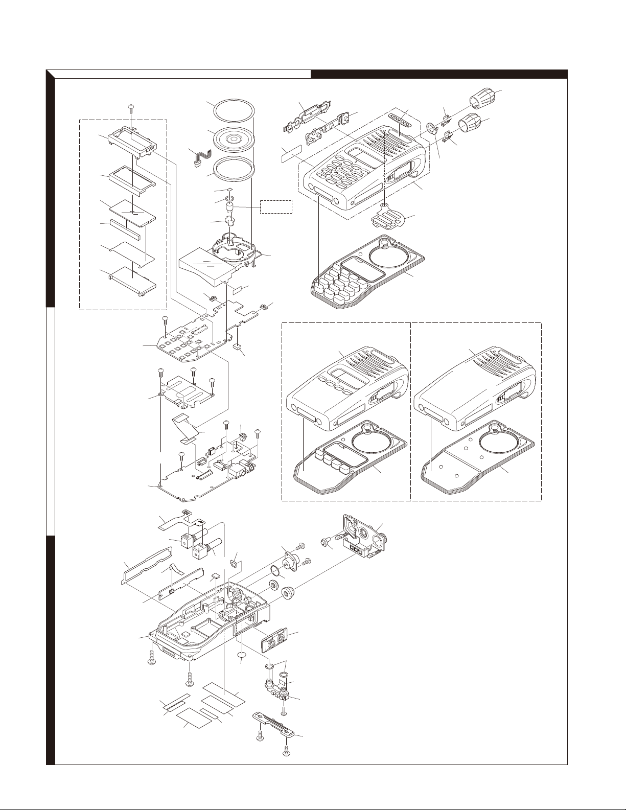
NX-320
51
EXPLODED VIEW
BA
F
34
56
57
700
27
65
21
12
27
59
58
31
1
11
20
29
36
46
X54
(C/3)
X54
MIC1
3 (K3,K6,E)
28
9
50
10
16 (K,K4,E3)
45
K2,K3,K5,K6,E,E2
Fx2
Display unit
(A54-376 A/3)
26
38
26
K2,K5,E2 K,K4,E3
21
39
Fx4
25
2
19
22
Fx10
30
TX-RX unit
(X57-805)
54
35
X54 (B/3)
S101
53
30
37
VR1
4
3
B
18
D
A
8
A
40
C
41
46x2
33
701
702
703
B
706
705
704
E
Parts with the exploded numbers larger than 700 are not supplied.
32
23
F
6
E
44 43
42
A : N09-2438-05
B : N09-6608-05
C : N14-0864-04
D : N14-0865-04
E : N30-3006-43
F : N83-2005-48
 Loading...