

Kenwood NX-200, NX-200GK2, NX-200G, NX-200K, NX-200(G) K Service Manual
VHF DIGITAL TRANSCEIVER
NX-200(G)
SERVICE MANUAL
© 2014-01 PRINTED IN JA PA N
RQ018 (K) B5B-7111-00
NX-200(G) K
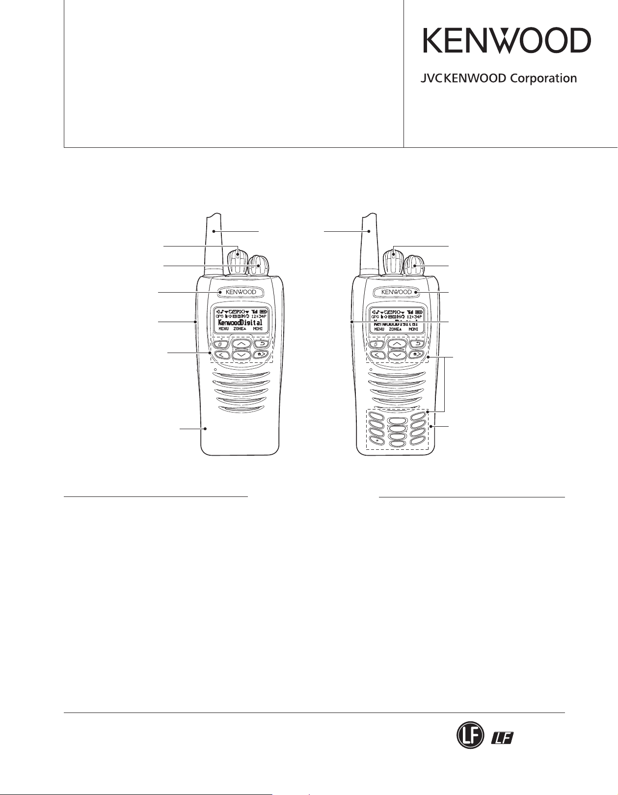
Knob (Selector)
(K29-9408-13)
Knob (Volume)
(K29-9407-03)
Badge
(B43-1606-14)
Knob (PTT)
(K29-9405-03)
Packing (6 key)
(G53-1765-11)
Plastic cabinet assy
(6 key)
(A02-4002-23)
NX-200(G) K2
Helical Antenna
(KRA-43G: option)
MIC
MIC
1
4
GH
I
7
PQRS
DEF
3
ABC
2
O
MN
6
JK
L
5
WXYZ
9
TUV
8
#
0
Knob (Selector)
(K29-9408-13)
Knob (Volume)
(K29-9407-03)
Badge
(B43-1606-14)
Knob (PTT)
(K29-9405-03)
Packing (18 key)
(G53-1766-11)
Plastic cabinet assy
(18 key)
(A02-4003-23)
CONTENTS
GENERAL .................................................................. 2
SYSTEM SET-UP ....................................................... 3
REALIGNMENT ......................................................... 3
INSTALLATION .......................................................... 6
DISASSEMBLY FOR REPAIR ................................... 8
CIRCUIT DESCRIPTION ......................................... 13
COMPONENTS DESCRIPTION .............................. 19
PARTS LIST ............................................................. 21
EXPLODED VIEW .................................................... 32
PACKING ................................................................. 33
TROUBLE SHOOTING ............................................ 34
ADJUSTMENT ......................................................... 39
TERMINAL FUNCTION ........................................... 61
PC BOARD
SUB (GPS) UNIT (X58-5240-10) ........................ 69
CONTROL UNIT (X53-4590-XX) ........................ 70
TX-RX UNIT (X57-8950-12) ................................ 74
INTERCONNECTION DIAGRAM ............................. 78
SCHEMATIC DIAGRAM .......................................... 80
BLOCK DIAGRAM .................................................. 94
LEVEL DIAGRAM ................................................... 98
OPTIONAL ACCESSORIES
KNB-47L (Li-ion Battery Pack) ......................... 99
KNB-48L (Li-ion Battery Pack) ......................... 99
KRA-43G (VHF,GPS Helical Antenna) .............. 99
SPECIFICATIONS ................................ BACK COVER
This product uses Lead Free solder.This product complies with the RoHs directive for the European market.

NX-200(G)
Document Copyrights
Copyright 2014 by JVC KENWOOD Corporation. All
rights reserved.
No part of this manual may be reproduced, translated,
distributed, or transmitted in any form or by any means,
electronic, mechanical, photocopying, recording, or otherwise, for any purpose without the prior written permission of
JVC KENWOOD Corporation.
Disclaimer
While every precaution has been taken in the preparation
of this manual, JVC KENWOOD Corporation assumes no
responsibility for errors or omissions. Neither is any liability
assumed for damages resulting from the use of the information contained herein. JVC KENWOOD Corporation reserves
the right to make changes to any products herein at any time
for improvement purposes.
Firmware Copyrights
The title to and ownership of copyrights for firmware
embedded in KENWOOD product memories are reserved
for JVC KENWOOD Corporation. Any modifying, reverse
engineering, copy, reproducing or disclosing on an Internet
website of the firmware is strictly prohibited without prior
written consent of JVC KENWOOD Corporation. Furthermore,
any reselling, assigning or transferring of the firmware is
also strictly prohibited without embedding the firmware in
KENWOOD product memories.
NXDN Transceivers:
The AMBE+2(TM) voice coding technology is embedded
in the fi rmware under the license of Digital Voice Systems,
Inc.
INTRODUCTION
SCOPE OF THIS MANUAL
This manual is intended for use by experienced technicians familiar with similar types of commercial grade communications equipment. It contains all required service information for the equipment and is current as of the publication
date. Changes which may occur after publication are covered by either Service Bulletins or Manual Revisions. These
are issued as required.
ORDERING REPLACEMENT PARTS
When ordering replacement parts or equipment information, the full part identifi cation number should be included.
This applies to all parts : components, kits, or chassis. If the
part number is not known, include the chassis or kit number
of which it is a part, and a suffi cient description of the required component for proper identifi cation.
2
GENERAL
PERSONAL SAFETY
The following precautions are recommended for personal
safety:
• DO NOT transmit until all RF connectors are verifi ed secure and any open connectors are properly terminated.
• SHUT OFF and DO NOT operate this equipment near
electrical blasting caps or in an explosive atmosphere.
• This equipment should be serviced by a qualifi ed technician only.
SERVICE
This transceiver is designed for easy servicing. Refer to
the schematic diagrams, printed circuit board views, and
alignment procedures contained within.
SYSTEM SET-UP
NX-200(G)
Merchandise received
Choose the type of transceiver
Transceiver programming
Are you using the optional antenna? Are you using the GPS function?
NO NO
Are you using the speaker microphone?
NO
Are you using the voice guide & storage unit?
NO
Frequency range (MHz) RF power Type
TX/RX 136~174 5W NX-200(G) K No
TX/RX 136~174 5W NX-200(G) K2
A personal computer, programming interface (KPG-36A/36U),
and programming software (KPG-111D)
are required for programming.
(The frequency, and signaling data are programmed for the transceiver.)
YES YES
KRA-22/KRA-26
Optional antenna
YES
KMC-41/KMC-42W/KMC-51/KMC-52
Speaker microphone
YES
VGS-1
(Option)
DTMF keypad
Yes
KRA-43G
Optional antenna
(Option)
(Option)
(Option)
See page 7.
1. Modes
User mode
Panel test mode
PC mode
Firmware
programming mode
Clone mode
Firmware version information
Delivery
PC test mode
REALIGNMENT
Panel tuning mode
Data programming mode
PC tuning mode
Mode
User mode For normal use.
Panel test mode
Panel tuning mode Used by the dealer to tune the transceiver.
PC mode
Data programming
mode
PC test mode
Firmware programming mode
Clone mode
Firmware version
information
Used by the dealer to check the fundamental characteristics.
Used for communication between the transceiver and PC.
Used to read and write frequency data and
other features to and from the transceiver.
Used to check the transceiver using the PC.
This feature is included in the FPU.
See pages 45 to 57.
Used when changing the main program of
the fl ash memory.
Used to transfer programming data from one
transceiver to another.
Used to confi rm the internal fi rmware version.
Function
3
NX-200(G)
REALIGNMENT
2. How to Enter Each Mode
Mode Operation
User mode Power ON
Panel test mode [
PC mode Received commands from PC
Panel tuning mode [Panel test mode] + [
Firmware programming
mode
Clone mode [
Firmware version
information
] + Power ON
] + Power ON
[
] + Power ON
[Side1] + Power ON
]
3. Panel Test Mode
Setting method refer to ADJUSTMENT.
4. Panel Tuning Mode
Setting method refer to ADJUSTMENT.
5. PC Mode
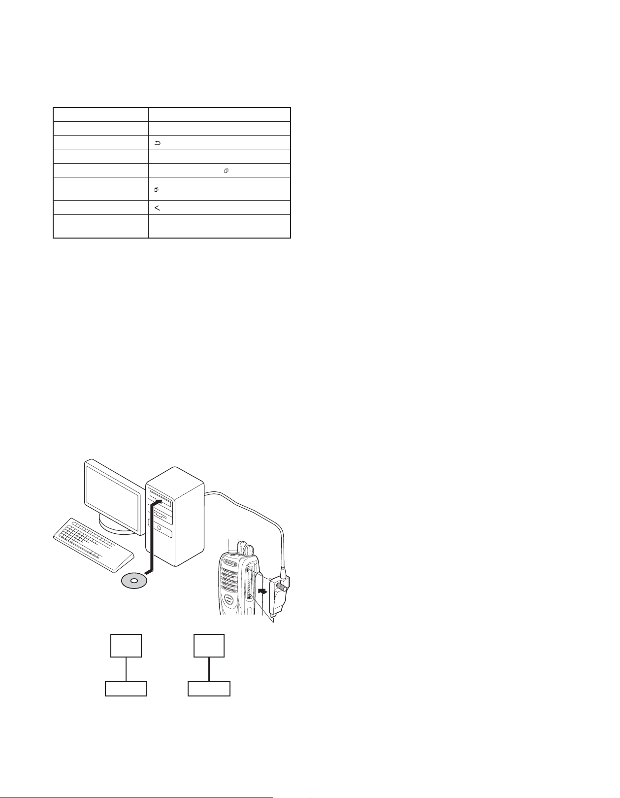
5-1. Preface
The transceiver is programmed by using a personal
computer, programming interface (KPG-36A/36U), and
FPU (programming software).
The programming software can be used with a PC.
Figure 1 shows the setup of a PC for programming.
PC
KPG-36A or KPG-36U
5-2. Connection procedure
1. Connect the transceiver to the computer using the interface cable (KPG-36A/36U). (Conection is the same as in
the PC Mode.)
Note:
• You must install the KCT-36U driver in the computer to
use the USB programming interface cable (KPG-36U).
2. When the POWER switch on, user mode can be entered
immediately. When PC sends command the transceiver
enter PC mode, and “PROGRAM” is displayed on the
LCD.
When data transmitting from transceiver, the red LED is
lights.
When data receiving to transceiver, the green LED is
lights.
Note:
The data stored in the computer must match the “Model
Name” when it is written into the fl ash memory.
5-3. KPG-36A description
(PC programming interface cable: Option)
The KPG-36A is required to interface the transceiver to
the computer. It has a circuit in its D-sub connector (KPG36A: 9-pin) case that converts the RS-232C logic level to the
TTL level.
The KPG-36A connects the universal connector of the
transceiver to the RS-232C serial port of the computer.
5-4. KPG-36U description
(PC programming interface cable: Option)
The KPG-36U is a cable which connects the to a USB
port on a computer.
When using the KPG-36U, install the supplied CD-ROM
(with driver software) in the computer. The KPG-36U driver
runs under Windows XP , Vista ,7 and 8.
The latest version of the USB driver is available for down-
load from the following URL:
http://www.kenwood.com/usb-com/
(This URL may change without notice.)
5-5. Programming software : KPG-111D/111DN
(Ver.4.40 or later) description
FPU
PC
D-SUB
(9-pin)
KPG-36A
Transceiver
PC
USB
KPG-36U
Transceiver
Fig. 1
The FPU is the programming software for the transceiver
supplied on a CD-ROM. This software runs under Windows
XP , Vista ,7 and 8 on a PC.
The data can be input to or read from the transceiver and
edited on the screen. The programmed or edited data can
be printed out. It is also possible to tune the transceiver.
6. Firmware Programming Mode
6-1. Preface
Flash memory is mounted on the transceiver. This al-
lows the transceiver to be upgraded when new features are
released in the future. (For details on how to obtain the fi rmware, contact Customer Service.)
4

REALIGNMENT
NX-200(G)
6-2. Connection procedure
Connect the transceiver to the personal computer using
the interface cable (KPG-36A/36U). (Connection is the same
as in the PC Mode.)
6-3. Programming
1. Start up the firmware programming software (Fpro.exe
(Ver. 6.20 or later)). The Fpro.exe exists in the KPG-
111D/111DN installed holder.
2. Set the communications speed (normally, 115200 bps)
and communications port in the confi guration item.
3. Set the fi rmware to be updated by File name item.
4. Press and hold the [
power ON. Then, the orange LED on the transceiver
lights and “PROGRAM 115200” is displayed.
5. Check the connection between the transceiver and the
personal computer, and make sure that the transceiver is
in the Program mode.
6. Press “write” button in the window. When the transceiver
starts to receive data, the [LOADING] display lights.
7. If writing ends successfully, the checksum is calculated
and a result is displayed.
8. If you want to continue programming other transceivers,
repeat steps 4 to 7.
] key while turning the transceiver
Note:
This mode cannot be entered if the Firmware Program-
ming mode is set to Disable in the Programming soft-
ware.
6-4. Function
1. If you press the [Side2] key while “PROGRAM 115200”
is displayed, the display changes to “PROGRAM 19200”
(The LED blinks green) to indicate that the write speed
is low speed (19200 bps). If you press the [Side2] key
again while “PROGRAM 19200” is displayed, the display
changes to “PROGRAM 38400” (The LED lights red
and orange alternatively). If you press the [Side2] key
again while “PROGRAM 38400” is displayed, the display
changes to “PROGRAM 57600” (The LED blinks orange).
If you press the [Side2] key again while “PROGRAM
57600” is displayed, the display returns to “PROGRAM
115200” (The LED lights orange).
2. If you press the [Side1] key while “PROGRAM 115200”
is displayed, the checksum is calculated, and a result is
displayed. If you press the [Side1] key again while the
checksum is displayed, “PROGRAM 115200” is redis-
played.
Note:
Normally, write in the high-speed mode.
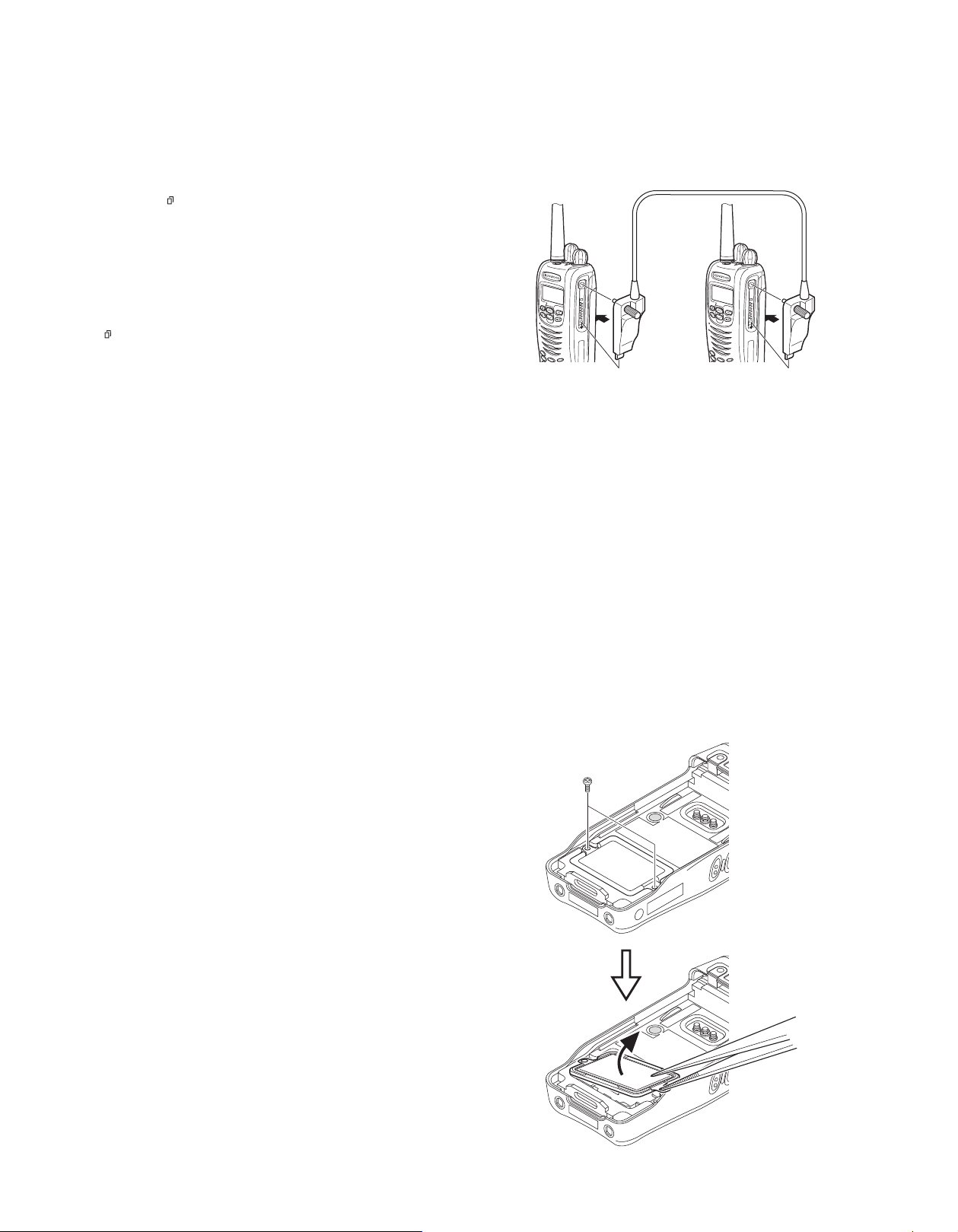
7. Clone Mode
Programming data can be transferred from one transceiver to another by connecting them via their external universal
connectors. The operation is as follows (the transmit transceiver is the source and the receive transceiver is a target).
The following data cannot be cloned.
• Tuning data
• Embedded message with password
• Model name data
• ESN (Electronic Serial Number) data
Note:
The following data can be cloned.
• Fleet (own)/ID (own) for FleetSync
• Unit ID (own) for NXDN
Key guide on the Read authorization password input screen.
• CONFRM ([
• DELETE ([
password number (Press and hold to delete all password
numbers)
• SELECT ([
word number
1. Press and hold the [
power ON. If the Read authorization password is set to
the transceiver, the transceiver displays “CLONE LOCK”.
If the password is not set, the transceiver displays “CLONE
MODE”.
2. When you enter the correct password, and “CLONE
MODE” is displayed, the transceiver can be used as the
cloning source. The following describes how to enter the
password.
3.
• How to enter the password using the keypad (K2
model only);
If one of keys 0 to 9 is pressed while the “CLONE LOCK”
is displayed, the pressed number is displayed on the
LCD.
Each press of the key shifts the display in order to the
left.
When you enter the password and press the [
key, “CLONE MODE” is displayed if the entered password
is correct. If the password is incorrect, “CLONE LOCK” is
redisplayed.
• How to enter the password using the [
keys ;
If the [
displayed, the Read authorization password input screen
is displayed.
If the [
authorization password input screen is displayed, the
number (0 to 9) blinks on the LCD. When you press the
[
] key, the currently selected number is determined. If
you press the [
procedure, “CLONE MODE” is displayed if the entered
password is correct. If the password is incorrect, “CLONE
LOCK” is redisplayed.
] key): The password confi rmation
] key): Delete the least digit from the current
] key): Determine the least digit of the pass-
] key while turning the transceiver
] or [ ]
] and [ ]
] / [ ] key is pressed while “CLONE LOCK” is
] key or [ ] key is pressed while the Read
] key after entering the password in this
5
NX-200(G)
REALIGNMENT
4. Power ON the target transceiver.
5. Connect the cloning cable (part No. E30-3325-05) to the
universal connectors on the source and target.
6. Press the [
“CLONE MODE”. The data of the source is sent to the
target. While the target is receiving the data, “PROGRAM”
is displayed. When cloning of data is completed, the
source displays “END”, and the target automatically operates in the User mode. The target can then be operated
by the same program as the source.
7. The other target can be continuously cloned. When the
[
] key on the source is pressed while the source displays
“END”, the source displays “CLONE MODE”. Carry out
the operation in step 4 to 6.
] key on the source while the source displays
Cloning cable
(E30-3325-05)
MI
C
1
4
GH
2
I
F
ABC
DE
3
Fig. 2
MI
C
1
4
GH
2
I
F
ABC
DE
3
Note:
• Cannot be cloned if the password (overwrite password) is
programmed to the target.
• “Model Name” must be same to clone the transceiver.
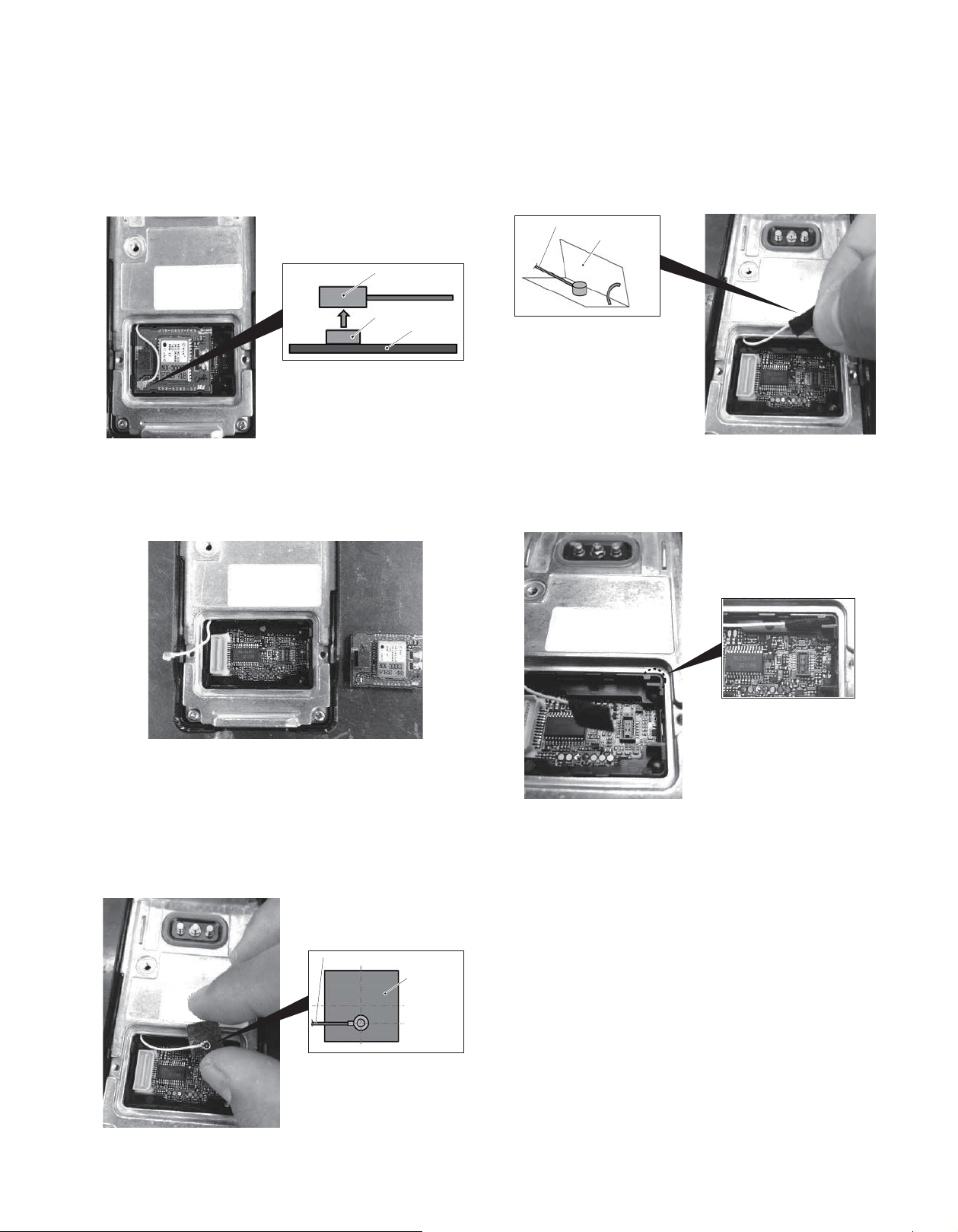
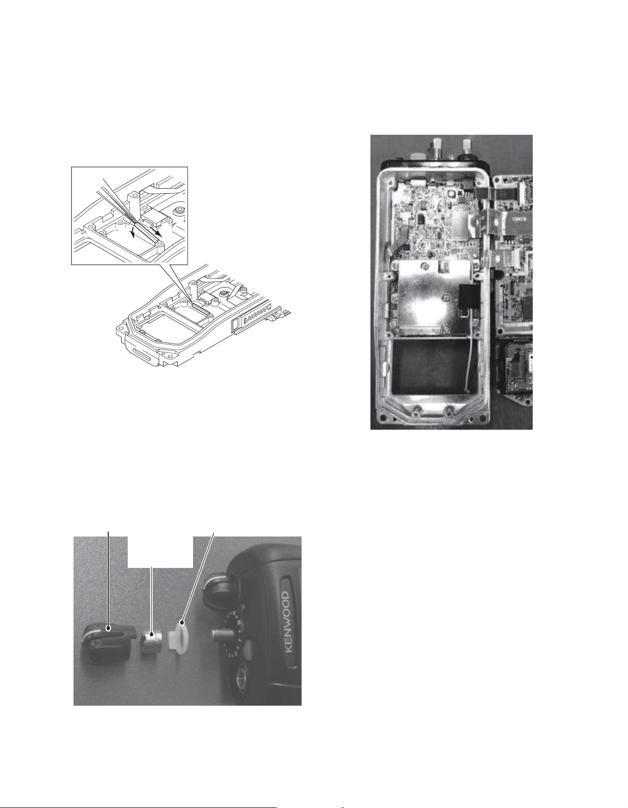
INSTALLATION
Preparation before Installing Option board
■
Removing the GPS PCB
1. Remove the two screws from the cover.
2. Remove the cover by inserting the tip of a pair of tweezers into the screw hole of the cover and prying it open.
8. Firmware Version Information
Press and hold the [Side1] key while turning the transceiver power ON and then keep pressing and holding the
[Side1] key, the fi rmware version information appears on the
LCD.
6
INSTALLATION
NX-200(G)
3. Remove the coaxial cable from the GPS PCB.
Note: When you remove the coaxial cable from the GPS
PCB, remove perpendicularly to the GPS PCB.
Coaxial cable
Coaxial connector
GPS PCB
4. Remove the GPS PCB from the connector (CN710) of
the Control PCB.
6. Fold the fi brous sheet (G11-1362-04) in half, and cover
the terminal of the coaxial cable as shown in the fi gure.
Coaxial cable
Fibrous sheet
(G11-1362-04)
7. Insert the fibrous sheet into the slit of the holder as
shown in the fi gure.
5. Affi x the terminal of the coaxial connector to the fi brous
sheet (G11-1362-04) as shown in the fi gure.
Coaxial cable
Fibrous sheet
(G11-1362-04)
7
NX-200(G)
INSTALLATION
Voice Guide & Storage Unit (VGS-1: Option)
■ Installing the VGS-1
. Attach the flat spring (G02-1846-03) to the VGS-1 as
1
shown in the fi gure.
Note:
Attach the fl at spring so that its convex fi ts the PCB hol-
low of the VGS-1.
2. Attach the cushion (G13-1974-04) to the VGS-1 as shown
in the fi gure.
Note:
Be sure to not cover the VGS-1 connector with the cush-
ion.
3. Insert the VGS-1 connector into the connector (CN710) of
the Control PCB.
4. Reinstall the cover using the two screws removed in step
1 of “Removing the GPS PCB” described on page 6.
VGS-1
VGS-1
PCB hollow
Convex part
Cushion
(G13-1974-04)
21x21x1.0mm
VGS-1
Flat spring
(G02-1846-03)
Flat spring
The coaxial cable is located under the GPS PCB.
DISASSEMBLY FOR REPAIR
1. Precautions for Waterproof
• Do not remove the black sheet from the reverse side of
the transceiver (refer to the illustration right). Removal
of this sheet decreases the waterproof effi ciency of the
transceiver and may cause malfunctions if water seeps
into the transceiver.
• The orange packing material on the reverse side of the
transceiver is important with respect to the waterproof ef-
fi ciency of the transceiver. Do not place stickers or other
materials on or around the packing material shown in the
fi gure, or on the reverse side of the battery pack. Doing
so will impair the waterproof effi ciency of the transceiver
and may cause it to break down. Additionally, in order to
prevent damage to the packing material, do not allow it to
come in contact with foreign materials.
CN710
Cushion
8
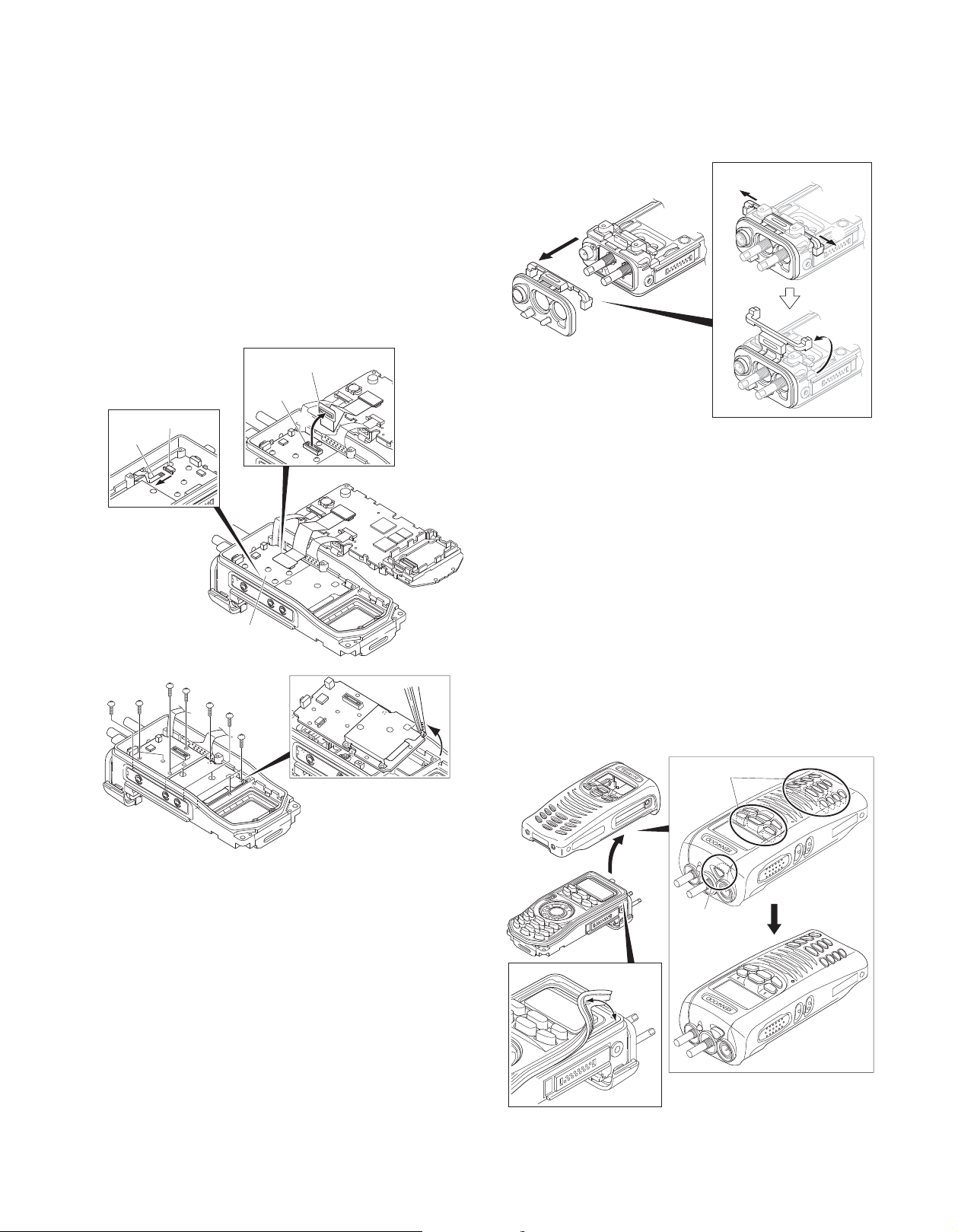
DISASSEMBLY FOR REPAIR
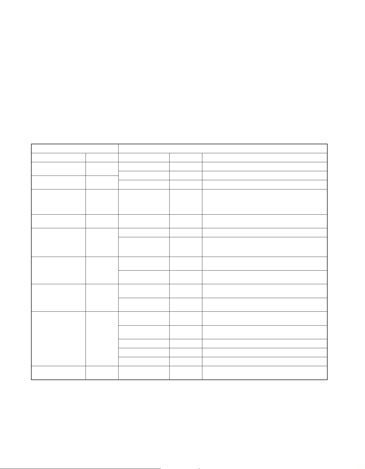
2. Precautions for Disassembly
■ Removing the TX-RX unit from the chassis
1. Remove the cord ASSY from the connector of the TX-RX
unit (CN400) a.
2. Remove the PTT FPC from the connector of the TX-RX
unit (CN401) b.
3. Remove the 14 screws c.
4. Anchor the screw hole of the TX-RX unit using the tip of a
pair of tweezers as shown in the fi gure. Then, lift the TXRX unit to remove it from the chassis d.
Cord ASSY
CN400
NX-200(G)
b
d
a
c
CN401
PTT FPC
b
TX-RX unit
c
c
c
Note:
The illustration of the Sub (GPS) unit and GPS
coaxial cable is omitted.
■
Removing the TOP packing (G53-1762-02)
1. Pull the TOP packing to the left to remove the packing
that is fi t into the left groove of the chassis a.
2. Pull the TOP packing to the right to remove the packing
that is fi t into the right groove of the chassis b.
3. Turn back the TOP packing as shown in the fi gure c.
4. Remove the TOP packing d.
c
c
c
c
a
d
3. Precautions for Reassembly
■ Mounting the chassis onto the case
1. Place the key top on the chassis. Then, fit the chassis
tightly into the groove of the key top a.
Note:
Confi rm that the entire groove of the key top fi ts to the
chassis tightly.
2. Mount the chassis onto the case b.
Note:
After mounting the chassis onto the case, if the 18-key
part on the key top or the Auxiliary (Orange) key part of
the VOL/CH packing gets stuck inside the case as shown
in the fi gure, return it to the normal position using a soft
tipped item (e.g., fi nger) c.
Prying it with a pointed metal tool such as forceps, may
damage the key top or packing.
18-key part
b
Auxiliary
(Orange) key
a
c
9
NX-200(G)
VOL/CH FPC
Univer
Conne
Cord ASSY
Note:
The illustration of the Sub (GPS) unit and GPS
coaxial cable is omitted.
DISASSEMBLY FOR REPAIR
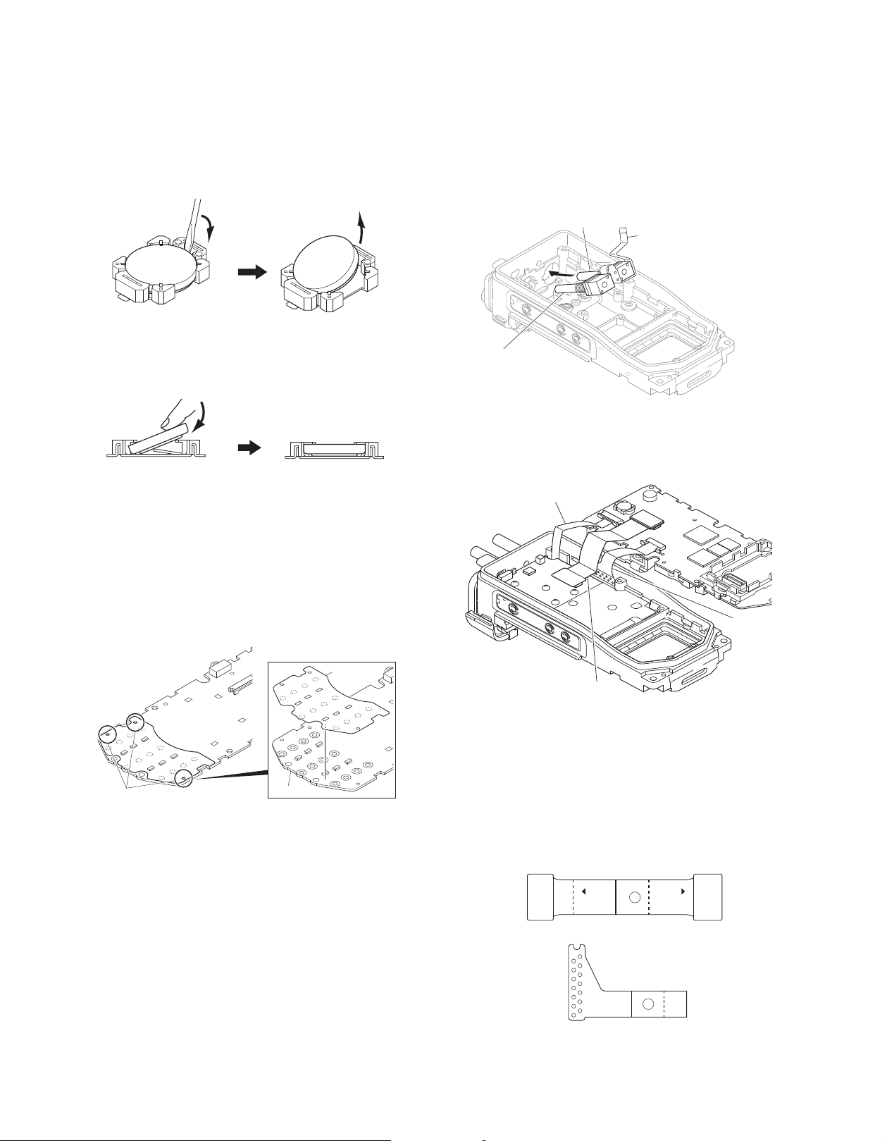
■
Removing the lithium cell (W09-0971-05)
Insert a non-conductive screwdriver to groove of one side
of the socket (CN401,CN11) and pry the lithium cell up
from the socket.
■
■
Installing the lithium cell (W09-0971-05)
Insert a lithium cell into one side of the socket (CN401,CN11).
Push the lithium cell to insert the lithium cell into the
socket.
■Affi xing the keyboard ASSY (S79-0472-05)
Affi x the keyboard ASSY to the Control unit as shown in
the fi gure.
After affixing the keyboard ASSY to the Control unit,
confi rm that the three positioning holes of the keyboard
ASSY and the Control unit are not misaligned.
Note:
If the holder (Option board) is removed from the Control
unit, it becomes easy to confirm the three positioning
holes.
■ Inserting the Volume and Channel switch into
the chassis
Insert the volume and channel switch into the chassis
with the VOL/CH FPC formed as shown in the fi gure.
Volume
VOL/CH FPC
Channel switch
■
Forming the VOL/CH FPC, Cord ASSY and Universal
connector FPC
Form the VOL/CH FPC, Cord ASSY and Universal con-
nector FPC as shown in the fi gure.
Positioning holes
Control unit
Keyboard
ASSY
Note:
Fold indications are printed on the Cord ASSY and Uni-
versal Connector FPC.
“––––” line shows creased line on the top.
“- - - -” line shows creased line on the bottom.
CONTTX-RX
J87-0005
Cord ASSY
J87-0007
Universal Connector FPC
10
DISASSEMBLY FOR REPAIR
b
a
NX-200(G)
■
Relay hardware (E29-1242-04) installation procedure
1. Fit one side of the relay hardware to a right corner of the
chassis using a pair of tweezers a.
2. Fit the other side of the relay hardware to the rib of the
chassis b.
Forming the GPS coaxial cable(E37-1716-05)
■
Form the GPS coaxial cable as shown in the fi gure.
■ Changing the channel selector from 16-channel
operation to free
1. Remove the channel selector knob.
2. Remove the circular nut.
3. Remove the mechanical stopper.
4. Reassemble the circular nut and channel selector knob
that were removed in steps 1 and 2, in their original positions.
Channel selector knob
(K29-9408-13)
Mechanical stopper
(D32-0446-14)
Circular nut
(N14-0844-04)
11
NX-200(G)
DISASSEMBLY FOR REPAIR
■
Assembly information (Sheet/Cushion)
When “Main Parts” is changed (ordered), “Assembled
Sheet/Cushion” should also be changed (ordered) together.
The Sticker and Sheet etc are non-reusable parts. It re-
quires the new one to get the radio’s performance after
repairs.
For example, when “Plastic Cabinet (A02-4002-23 (6-key)/
A02-4003-23 (18-key))” is changed, “Sticker (B42-7417-
04)”, “Badge (B43-1606-04)” and “Fibrous Sheet (G101373-04)” should be ordered and changed together because Sticker (B42-7417-04), Badge (B43-1606-04) and
Fibrous Sheet (G10-1373-04) are non-reusable.
Main Parts Assembled Sheet/ Cushion
Part Name Part Number Part Name Part Number Remark
Plastic Cabinet (6-key) A02-4002-23
Plastic Cabinet (18-key) A02-4003-23
LCD ASSY B38-0923-05 Adhesive Sheet (LCD) J99-0714-04
Cord ASSY (50-pin
FPC)
Speaker T07-0755-25
Switch Unit (6-key FPC) X41-3840-10
Switch Unit (PTT FPC) X41-3830-10
Chassis A10-4186-04
Terminal Block E72-0425-03
X42-3510-10 Cushion (50-pin FPC) G13-2293-04
Sticker B42-7417-04 “NEXEDGE” is printed.
Badge B43-1606-04 “KENWOOD” is printed.
Fibrous Sheet (SP) G10-1373-04
Rubber Cushion (SP) G11-4272-14
Sheet (SP) G11-4458-14
Adhesive Sheet
(6-key FPC)
Adhesive Sheet
(6-key FPC)
Sheet (PTT) G11-4428-04
Adhesive Sheet
(PTT FPC)
Relay Hardware
(VCO-Chassis)
Sheet (Air) G11-4500-04
Rubber Sheet (FET) G11-4429-04 Used for stabilizing the radiation performance of the FET.
Sheet (Air) G11-4440-04 This sheet is a protect cover of the sheet (G11-4331-04).
Cushion (ANT) G13-2220-04 Used for fi xing the Terminal ASSY.
Adhesive Sheet
(Terminal Block)
Used for fi xing the LCD ASSY on the Illumination Guide
(LCD).
Also used for fi xing the Illumination Guide (LCD) on the
Control Unit.
Used for stabilizing the waterproof performance.
“•” (a hole) on the Sheet (SP) shows the upper side (6-key
FPC side).
J99-0745-04
J99-0712-14
J99-0711-04 Used for fi xing the Switch Unit (PTT FPC) on the Chassis.
E29-1221-14 Used for stabilizing the shield performance of the VCO.
J99-0747-04
Used for fi xing the Switch Unit (6-key FPC) from the back
side of the Holder (FG-SP) before soldering.
Used for fi xing the Switch Unit (6-key FPC) on the Holder
(FG-SP).
Used for fi xing the Push Knob (PTT) on the Switch Unit (PTT
FPC) and stabilizing the waterproof performance.
This sheet is put on the leak check hole.
This sheet lets air through, but does not let water through.
Used for fi xing the Terminal Block and the Packing (Terminal
Block).
12
CIRCUIT DESCRIPTION
NX-200(G)
1. Overview
The NX-200(G) is a VHF portable transceiver designed
to operate in the frequency range of 136 to 174MHz. The
unit consists of receiver, transmitter, phase-locked loop (PLL)
frequency synthesizer, base band parts, power supply, and
control circuits.
ANT
TX/RX: 136~174MHz
ANT
SW
PA
AMP
RF
AMP
TX
AMP
1st MIX
136~174MHz
MCF
58.05MHz
19.2MHz
VC
TCXO
194.05~232.05MHz
Fig. 1 Frequency confi guration
3. Receiver System
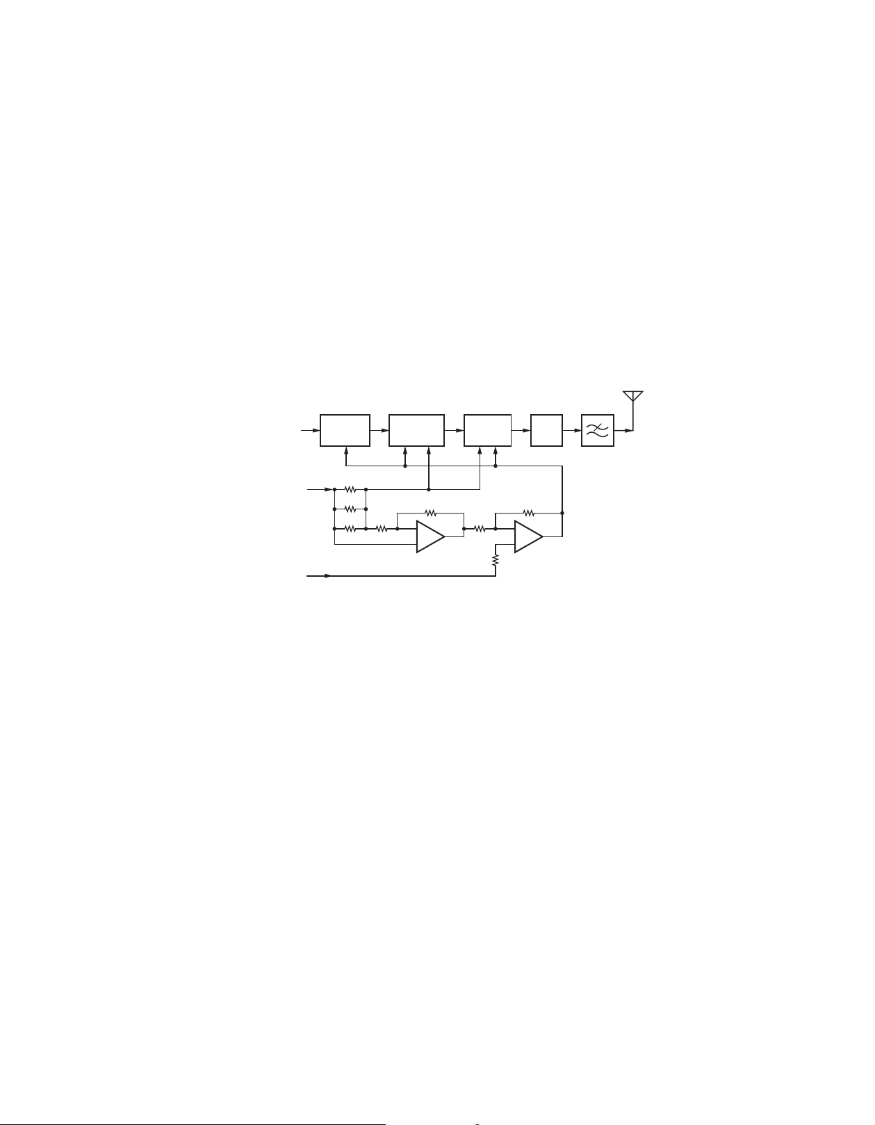
3-1. RF Circuit
An incoming RF signal from the antenna terminal is
passed through the antenna switch (D104, D105, D209
and D211) and then the bandpass fi lter (L220, L224). The
bandpass fi lter is adjusted by a variable capacitor. The input
voltage to the variable capacitor is regulated by the voltage
output from the D/A converter (IC703). The signal is amplified by an RF amplifier (Q204), and passed through the
bandpass fi lter (L212, L215). The resulting signal is applied
to the fi rst mixer (Q203), where it is mixed with the fi rst local oscillator signal output from the frequency synthesizer to
produce the fi rst IF (58.05MHz).
ANT
L109,L110,
L113
L220,L224
ANT
SW
D104,D105
D209,D211
IC704 IC707
IC108
ASIC
IC102
DSP
AMT
RF AMP
Q204
L212,L215
1st PLL OSC (PLL)
IC713
(2/2)
IC703
VOL
x3
1st MIX
Q203
IC408
2. Frequency Confi guration
The receiver is a double-conversion superheterodyne using the fi rst intermediate frequency (IF) of 58.05MHz and the
second IF of 450kHz. Incoming signals from the antenna are
mixed with the local signal from the PLL circuit to produce
the fi rst IF of 58.05MHz. This is then mixed with the 57.6MHz
second local oscillator output to produce the 450kHz second
IF. The transmit signal frequency is generated by the PLL
VCO, and modulated by the signal from the DSP. It is then
amplifi ed and fed to the antenna.
CF
450kHz
SP
MIX
IF AMP
57.6MHz
PLL
VCO
3-2. IF Circuit
The fi rst IF signal is passed through a four-pole monolithic crystal fi lter (XF200) to reject adjacent channel signals.
The fi ltered fi rst IF signal is amplifi ed by the fi rst IF amplifi er
(Q202) and then applied to the lF system IC (IC202). The
IF system IC provides a second mixer, AGC amplifi er, and
RSSI (Received Signal Strength Indicator).
The second mixer mixes the first IF signal with the
57.6MHz of second local oscillator output and produces the
second IF signal of 450kHz.
The second IF signal is passed through the ceramic fi lter
(CF200) to reject the adjacent channel signal. The fi ltered
second IF signal is amplifi ed by the AGC amplifi er.
The signal from the AGC amplifi er is input to the ASIC
(IC108) through the ceramic fi lter (CF201) and operational
amplifi er (IC203).
IF AMP
MCF
XF200
IC409
X1
VC
TCXO
19.2MHz
SWSW
Q202
2nd OSC
x3
Q201
IC413
IC412
AF
AMP
Base band circuit
MIC
AMP
IC202
MIX, AGC
CF200
MIC
INT. SP
EXT. SP
CF201
IC203
INAMT
EXAMT
Fig. 2 RF and IF circuit
13
NX-200(G)
CIRCUIT DESCRIPTION
3-3. Audio Amplifi er Circuit
Audio processing (high-pass filter, low-pass filter, deemphasized and so on) at FM mode and decoding at NXDN
mode are processed by DSP. The audio signal from IC108
and IC102 goes through the amplifier (IC704). The signal
then goes through a mute switch (IC707), amplifi er (IC713),
electronic volume control (IC703), and AF amplifi er (IC408).
While busy, AMT becomes Low to turn IC707 on, and the
signal is fed to the AF switch. While INAMT is High, the AF
switch (IC409) selects the internal speaker, and the audio
signal is fed to the internal audio power amplifi er (IC413),
and output to the internal speaker. While EXAMT is High, the
AF switch (IC409) selects the external speaker, and the audio signal is fed to the external audio power amplifi er (IC412),
and output to the external speaker. The power supply for
IC413 and IC412 is turned on while INAMT or EXAMT is
High.
The speaker is switched by the logic of the speaker
switching terminal SSW on the universal connector. When
the SP-MIC is not attached, SSW becomes High. IC108
detects the logic of SSW and activates either INAMT or EXAMT.
B
INAMT
EXAMT
AF signal
from IC408
Q406
Q405
IC409
VDD
IC413
SHUT DOWN
VDD
IC412
SHUT DOWN
INT. SP
EXT. SP
Fig. 3 Audio amplifi er circuit
3-4. Squelch Circuit
It amplifies the demodulated noise signal from IC108
after fi ltering through the BPF circuit. Then, the amplifi ed signal is converted to a DC signal by the detection circuit. The
converted signal is fed back to IC108.
DET
IC108
ASQAPC
ASQDET
IC702
(1/2)
LPF
IC711
(2/2)
HPF
Q704
AMP
D705
RECT
IC711
(1/2)
AMP
Fig. 4 Squelch circuit
4. Transmitter System
4-1. Audio Band Circuit
The signal from the internal microphone goes through
the mute switch (Q5). When the SP-MIC is not attached, the
microphone switching terminal (MSW) on the universal connector becomes High, and the mute switch (Q5) is turned
on. When the SP-MIC is attached, MSW is connected to
GND inside the SP-MIC. For this reason, Q5 is turned off,
the internal microphone is muted, and only the input of the
external microphone is supplied to the microphone amplifi er. The signal from the microphone goes through the mute
switch (Q707), and is amplifi ed by IC716 (1/2) and limited
by the AGC circuit which is composed of D703, D704, Q705
and Q706.
4-2. Base Band Circuit
The audio signal output from the base band circuit is converted to digital data with a sampling frequency of 48kHz.
This digital data is sent to the DSP (IC102), and voice signals of 300Hz or lower and frequencies of 3kHz or higher
are cut off and an audio range of 300Hz to 3kHz is extracted.
The audio signal is then pre-emphasized in FM mode and
synthesized with the signals, such as QT and DQT, as required, and is then output from IC108. In Digital mode, the
audio signal is converted to the 4-Level FSK base band signal and output from IC108. The DTMF and MSK base band
signals are also generated by the DSP and output by IC108.
LPF (IC705) works as a smoothing fi lter. The DAC (IC703)
assigns the base band signal to the VCO and VCTCXO (X1).
At this time, the level output according to the transmit carrier
is fi ne-adjusted according to each modulation method.
14
EXT. MIC
INT. MIC
Q5
SW
MSW
IC716
Q707 IC712
SW
MM
Q4
D703,D704
Q705,Q706
(1/2)
AMP
AGC
IC102
DSP
IC108
ASIC
IC705
(2/2)
LPF
IC705
(1/2)
LPF
SW
SCSW
IC710
(1/2)
AMP
IC706
LPF
Fig. 5 Audio band and Base band circuit
IC710
(2/2)
AMP IC703
IC5
AMP
AMP
IC4
(1/2)
X1
VCTCXO
VCO
CIRCUIT DESCRIPTION
NX-200(G)
4-3. VOX
IC716 (2/2) amplifi es the audio signal captured in the microphone. The signal is then converted into the DC voltage,
rectifi ed by D706. The DC voltage activates the ASIC (IC108),
and the VOX starts.
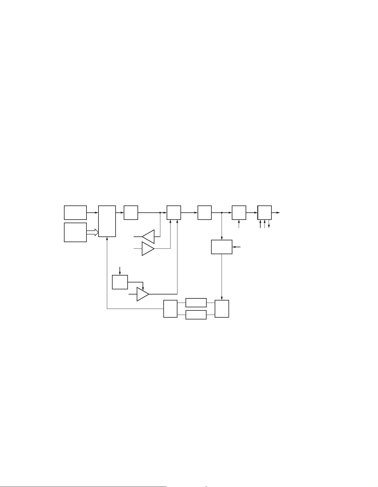
4-4. Drive and Final Amplifi er
The signal from the T/R switch (D100 is on) is amplifi ed
by the drive amplifi er (Q102 and Q103) to 25~27dBm. The
output of the drive amplifi er is amplifi ed by the Final power
amplifi er (Q106) to 5.0W (1W when the power is low). The
Final power amplifi er is MOS FET. The output of the Final
power amplifi er is then passed through the harmonic fi lter
(LPF) and antenna switch (D104, D105 are on) and applied
to the antenna terminal.
From
T/R SW
(D100)
+B
Q102
Pre-Drive
AMP
R136
R138
R141
Q103
Drive
AMP
4-5. APC Circuit
The APC circuit always monitors the current flowing through the Final power amplifier (Q106) and keeps
a constant current. The voltage drop at R136, R138
and R141 is caused by the current flowing through
the RF power amplifier and this voltage is applied to
the differential amplifier (IC100 1/2). IC100 (2/2) compares the output voltage of IC100 (1/2) with the reference voltage from IC108, and the output of IC100
(2/2) controls the VGG of Q102, Q103 and Q106 to make
the both voltages the same. The change of power high/low
is carried out by the change of the reference voltage. Q105,
Q107 and Q110 are turned on and Q104 and Q109 are
turned off in transmit and the APC circuit is active.
ANT
D104,D105Q106
Final
AMP
VDD
ANT
SW
VGG
REF
VOL
(IC108)
Fig. 6 Drive and fi nal amplifi er and APC circuit
5. PLL Frequency Synthesizer
5-1. VCTCXO (X1)
VCTCXO (X1) generates a reference frequency of
19.2MHz for the PLL frequency synthesizer. This reference
frequency is applied to pin 9 of the PLL IC (IC3) and is connected to the IF circuit as a 2nd local signal through the
Tripler (Q201). The VCTCXO oscillation frequency is determined by the DC voltage of the VC terminal. The VC voltage
is fi xed to 1.65V by R59 and R60, and supplied to the VC
terminal through IC5. The modulation signal is also fed to VC
terminal through IC5.
The frequency adjustment is achieved by switching the
ratio of dividing frequency that is not adjusted by the DC
voltage impressed to VC. The resolution of the adjusting frequency is approximately 8Hz. Because twice the VCO output
are input for the input frequency of PLL IC, the sending and
receiving frequency can be adjusted by approximately 4Hz
resolution.
IC100
(1/2)
IC100
(2/2)
5-2. VCO
There is a RX VCO and a TX VCO.
The TX VCO (Q10) generates a transmit carrier and the
RX VCO (Q8) generates a 1st local signal. For the VCO
oscillation frequency, the transmit carrier is 136 to 174 MHz
and the 1st local receive signal is 194.05 to 232.05MHz.
The VCO oscillation frequency is determined by one system of operation switching terminal “T/R” and two systems of
voltage control terminals “CV” and “ASSIST”.
The operation switching terminal, “T/R”, is controlled by
the control line (/T_R) output from the ASIC (IC108). When
the /T_R logic is low, the VCO outputs the transmit carrier
and when it is high, it outputs a 1st local receive signal.
The voltage control terminals, “CV” and “ASSIST”, are
controlled by the PLL IC (IC3) and ASIC (IC108) and the
output frequency changes continuously according to the
applied voltage. For the modulation input terminal, “VCO_
MOD”, the output frequency changes according to the applied voltage. This is used to modulate the VCO output.
“VCO_MOD” works only when “/T_R” is low.
15
NX-200(G)
CIRCUIT DESCRIPTION
5-3. PLL IC (IC3)
The PLL IC compares the differences in phases of the
VCO oscillation frequency and the VCTCXO reference
frequency, returns the difference to the VCO CV terminal
and realizes the “Phase Locked Loop” for the return control. This allows the VCO oscillation frequency to accurately
match (lock) the desired frequency.
When the frequency is controlled by the PLL, the frequency convergence time increases as the frequency difference increases when the set frequency is changed. To supplement this, the ASIC is used before control by the PLL IC
to bring the VCO oscillation frequency close to the desired
frequency. As a result, the VCO CV voltage does not change
and is always stable at approximately 2.5V.
The desired frequency is set for the PLL IC by the ASIC
(IC108) through the 3-line “SDO1”, “SCK1”, “/PCS_RF” serial bus. Whether the PLL IC is locked or not is monitored by
the ASIC through the “PLD” signal line. If the VCO is not the
desired frequency (unlock), the “PLD” logic is low.
X1
19.2MHz
VC
TCXO
SDO1
SCK1
/PCS_RF
IC3 Q11
PLL
IC
Loop
Filter
Q12
CV
VCO_MOD
150C
Q3
Ripple
Filter
ASSIST
Q8,Q10
D8,D9,D12~D17
VCO
IC4 (1/2)
IC2
RF
SW
D2,D3
5-4. Doubler (Q4)
The doubler (Q4) extracts the twice harmonic component
from the signal from the VCO. This twice harmonic components is then fed into PLL (IC3) through band pass fi lter.
Band pass filter is consists of two filter. One is for TX
(L3,L5,L7) and pass band is 272.0 to 348.0MHz. The other
is for RX 1st local (L2,L6,L30) and pass band is 388.1 to
464.1MHz.
5-5. Local Switch (D100, D201)
The connection destination of the signal output from the
buffer amplifier (Q100) is changed with the diode switch
(D100) that is controlled by the transmission power supply,
50T, and the diode switch (D201) that is controlled by the
receive power supply, 50R. If the 50T logic is high, it is connected to a send-side pre-drive (Q102). If the 50T logic is
low, it is connected to a receive-side mixer (Q203).
BUFF
AMP
L2,L6,L30
BPF(RX)
BPF(TX)
L3,L5,L7
Q100
BUFF
AMP
Doubler
Q4
RF
SW
D5,D6
50C
50C
D100,D201
T/R
SW
50T
50R
to 1st Mixer
to TX stage
Fig. 7 PLL block diagram
6. Control Circuit
The control circuit consists of the ASIC (IC108) and its
peripheral circuits. IC108 mainly performs the following;
1) Switching between transmission and reception by PTT
signal input.
2) Reading system, zone, frequency, and program data from
the memory circuit.
3) Sending frequency program data to the PLL.
4) Controlling squelch on/off by the DC voltage from the
squelch circuit.
5) Controlling the audio mute circuit by decode data input.
16
6-1. ASIC
The ASIC (IC108) is a 32-bit RISC processor, equipped
with peripheral function and ADC/DAC.
This ASIC operates at 18.432MHz clock and 3.3V /1.5V
DC. It controls the fl ash memory, SRAM, DSP, the receive
circuit, the transmitter circuit, the control circuit, and the display circuit and transfers data to or from an external device.
CIRCUIT DESCRIPTION
NX-200(G)
6-2. Memory Circuit
The memory circuit consists of the ASIC (IC108) and the
SRAM (IC103) and fl ash memory (IC101). The fl ash memory
has capacity of 32M-bit that contains the transceiver control
program for the ASIC and stores the data. It also stores the
data for transceiver channels and operating parameter that
are written by the FPU. This program can be easily written
from external devices. The SRAM has capacity of 1M-bit that
contains work area and data area.
Flash memory
■
Note: The flash memory stores the data that is written by
the FPU (KPG-111D), tuning data (Deviation, Squelch,
etc.) ,and fi rmware program (User mode, Test mode, Tuning
mode, etc.). This data must be rewritten when replacing the
fl ash memory.
SRAM (Static memory)
■
Note: The SRAM has temporary data area and work area.
When the power supply is off, it is backed up by an internal
secondary lithium battery. Therefore, the saved data is not
lost.
Real-time clock
■
The clock function is based on real-time clock IC (IC106).
When the power supply is off, it is backed up by an internal
secondary lithium battery.
6-3. LCD
The LCD is controlled using the bus lines on the connector (CN1) of the Control unit (X53-426). It corrects the LCD
contrast voltage using IC1.
6-4. Key Detection Circuit
Keys are detected using the key scan circuit in IC108.
The /KEYI signals that are normally pulled down go high
when any key is pressed.
6-5. Low Battery Warning
The battery voltage is divided using R444 and R445 and
is detected by the ASIC (IC108). When the battery voltage
falls below the voltage set by the Low battery warning adjustment, the red LED blinks to notify the operator that it is
time to replace the battery. If the battery voltage falls even
more (approx. 5.8V), a beep sounds and transmission stops.
Low battery warning Battery condition
The red LED blinks during
transmission.
The red LED blinks and the
warning tone beeps while the
PTT switch is pressed.
The battery voltage is low but
the transceiver is still usable.
The battery voltage is low and
the transceiver is not usable to
make calls.
6-6. DSP
The DSP circuit consists of a DSP (IC102) and processes the base band signal. The DSP operates on an external
clock of 18.432MHz (the same as the IC108), the I/O section
operates at 3.3V and the core section operates at 1.5V. The
DSP carries out the following processes:
• 4 Level FSK processing
• Analog FM pre-emphasis/de-emphasis
• Vocoder processing between audio codec and modula-
tion/demodulation
• CAI processing, such as error correction encoding
• QT/DQT encoding/decoding
• LTR encoding/decoding
• DTMF encoding/decoding
• MSK encoding/decoding
• 2-tone encoding/decoding
• Compressor/expander processing
• Voice scrambler processing
• Transmit/receive audio fi ltering processing
• Microphone amplifi er AGC processing
• Audio mute processing
• Modulation level processing
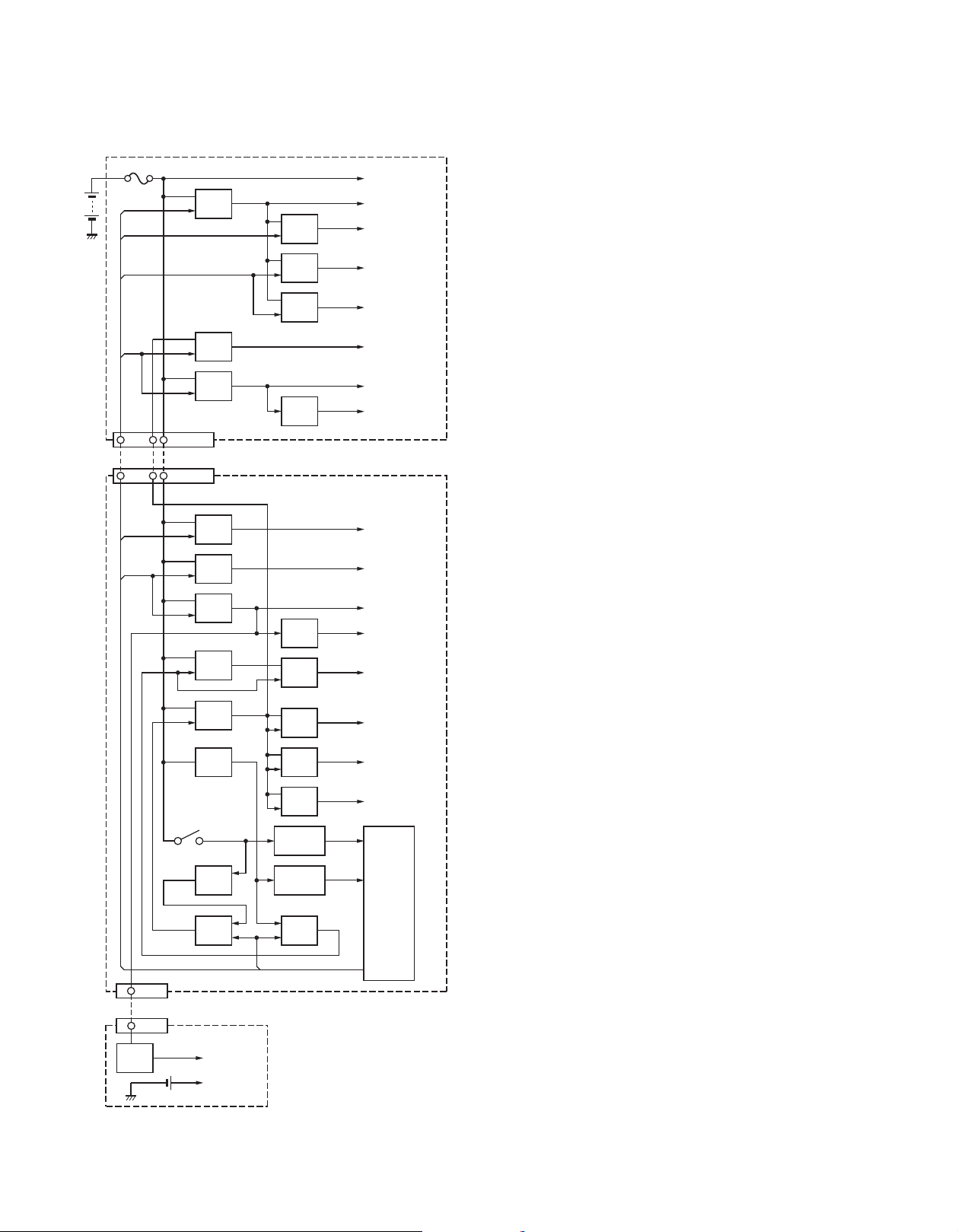
7. Power Supply Circuit
The battery voltage (+B) is provided from the battery
terminal on the TX/RX unit (X57). The battery voltage passes
through the 2.5A fuse (F400), and goes to the RF fi nal amplifi er, AVR ICs (IC400, IC403), and Control unit (X53-426).
In the control unit, +B is connected to the DC/DC (IC407),
AVR ICs (IC411, IC708, IC416), and voltage detector IC
(IC414). The voltage detector watches the battery voltage.
If the battery voltage is 5.6V or higher, the detector outputs
High. While the output of IC414 is High, IC416 and Q409
provide 3.1V (31BU) to the backup-section.
When the VOL SW is turned on, SB1 becomes high (battery voltage). The DC/DC (IC407) operates if both SB1 and
the output of the detector are high. IC407 outputs 3.8V and it
activates IC404 (33M), IC717 (15M), and IC406 (33A). As a
result, the ASIC and DSP operate.
The SBC signal becomes High after the ASIC operates,
IC708 (5A), Q403 on the Control unit (SB2) and Q403 on the
TX-RX unit (SB3) are turned on. IC402 and IC403 operate
by turning on these AVR ICs and FET switches.
The 5UC signal becomes High when an option is installed on the universal connector. Then IC411 (50U) operates.
When the /SAVE signal becomes High, IC400 (50C)
operates. The output of IC400 is connected to three FET
switches (Q401, Q402, Q405). When the SBC signal
becomes High, IC403 (33C) operates. The FET switches are
controlled by the ASIC. Q405 (50T) is turned on in transmit
mode. Q401 (50R) and Q402 (50IF) are turned on in receive
mode.
When the VOL SW is turned off, the /PSW signal
becomes Low. After detecting the /PSW signal, the ASIC
changes the SBC signal to Low. Then the power supplies
except IC416 (31BU) stop.
17
NX-200(G)
CIRCUIT DESCRIPTION
F400
2.5A
/SAVE
/5TC
5RC
SBC
5UC
SBC
5A
VOL SW
CN710
IC400
IC403
AVR IC
SB3 SW
CN400
CN404
IC411
AVR IC
SB2 SW
IC708
AVR IC
IC416
AVR IC
IC407
DC/DC
IC414
Detect
AVR
Q403
Q403
SB1
Q408
AND
D408
OR
SBC
Q405
50T SW
Q401
50R SW
Q402
50IF SW
IC402
DC/DC
IC403
DC/DC
Q409
31BU
IC404
AVR
IC717
DC/DC
IC406
AVR
Q402
Lvl Conv
Q401
Lvl Conv
D412
OR
+B
50C
50T
50R
50IF
33C
SB3
150C
50U
SB2
5A
-10V
31BU
33M
15M
33A
/PSW
/BINT
TX-RX unit (X57)
RF Final AMP
APC
VCO
TX circuit
RX circuit
IF circuit
PLL, VCTCXO
TX/Busy LED
Assist, Tune
Control unit (X53)
Universal
BackLight
Key Light
Option
LCD Bias
SRAM, RTC
ASIC, DSP I/O,
Flach, LCD DRV
ASIC, DSP core
ASIC Analog,
Audio
IC108
ASIC
8. Signaling Circuit
8-1. Encode (QT/DQT/LTR/DTMF/2-tone/MSK)
Each signaling data signal of QT, DQT, LTR, DTMF,
2-tone and MSK is generated by the DSP circuit, superposed on a modulation signal and output from IC108. The
modulation balance of the QT/DQT/LTR signal is adjusted by
the D/A converter(IC703) and the resulting signal is routed
to the modulation input of the VCO and VCXO (X1). Each
deviation of the TX QT, DQT, LTR, DTMF, 2-tone and MSK
tone is adjusted by changing the output level of IC108 and
the resulting signal is routed to the VCO and VCXO. The RX
DTMF tone is routed to the receive audio signal system, and
is output from the speaker.
8-2. Decode (QT/DQT/LTR/DTMF/2-tone/MSK)
The audio signal is removed from the FM detection signal
sent to the DSP circuit and the resulting signal is decoded.
9. Compander Circuit
The term “compander” means compressor and expander.
The compander reduces noise by utilizing a compressor
and an expander. The transceiver contains a DSP (IC102) to
perform this operation. The transceiver compander can be
turned on or off using the FPU.
10. GPS Circuit
The GPS information function can be used by setting it
through the FPU. When the GPS information function is
enabled, the AVR (IC4/GPS) is enabled by the OPT5, and is
supplied to the GPS circuit.
The GPS circuit block consists of a TX-RX unit and
a GPS unit (X58). The circuit from an antenna to LNA is on
a TX-RX unit. This output is connected to the GPS unit by
the coaxial cable.
The GPS signal of 1575.42MHz received with the antenna (with GPS band) is passed by the HPF and BPF (L605/
TX-RX) and is amplifi ed by the LNA (IC881/TX-RX).
The GPS signal is processed by the GPS IC (IC1/GPS)
and input to the ASIC (IC108/CONT) through the UART port.
The ASIC (IC108/CONT) processes the GPS data (NMEA)
and sends the resulting information to the LCD.
The GPS IC operates in stand-alone. Operating voltage
is 3.1V. When the transceiver power is off, the GPS IC will
be backed up with the internal coin battery. When the battery
pack is removed, the GPS IC will be backed up for about
one day in a coin battery. But if the GPS IC has never had
the position fi xed, it will not be backed up.
When the GPS function is enabled, the consumption current increases by about 70 mA.
18
IC4
AVR IC
Sub (GPS) unit (X58)
CN10
Lithium cell
31V
GPS module
Buffer
V_BCKP
Fig. 8 Power supply circuit
NX-200(G)
COMPONENTS DESCRIPTION
Control unit (X53-4590-XX)
Ref. No. Part Name Description
IC1 IC LCD contrast
IC101 IC FLASH ROM
IC102 IC DSP
IC103 IC SRAM
IC104 IC 2 input AND gate
IC105 IC Reset
IC106 IC RTC
IC107 IC Buffer
IC108 IC ASIC
IC109 IC 2 input AND gate
IC401,402 IC Bus switch
IC403 IC Voltage doubling inverter
IC404 IC Voltage regulator (33M)
IC406 IC Voltage regulator (33A)
IC407 IC DC/DC converter
IC408 IC AF AMP
IC409 IC AF switch
IC411 IC Voltage regulator (50U)
IC412,413 IC Audio AMP
IC414 IC Reset
IC415 IC 2 input AND gate
IC416 IC Voltage regulator
IC417,418 IC Dual bus buffer
IC701 IC I/O control
IC702 IC APC LPF
IC703 IC D/A converter
IC704 IC RX AF LPF
IC705 IC Modulation LPF
IC706 IC MIC AMP
IC707 IC RX AF switch
IC708 IC Voltage regulator (5A)
IC709 IC Sidetone mute
IC710 IC MOD/MIC summing AMP
IC711 IC SQL BPF/SQL DC AMP
IC712 IC MIC switch
IC713 IC 1.65V REF/RX summing AMP
IC714 IC OPT switch
IC715,716 IC VOX AMP
IC717 IC DC/DC converter (15M)
Q1,2 Transistor LCD backlight switch
Q3 FET LCD backlight switch
Q4 FET MIC mute control
Q5 FET MIC mute switch
Q101,102 Transistor 12key backlight switch
Ref. No. Part Name Description
Q103 FET 12key backlight switch
Q401,402 FET Level converter
Q403 Transistor SB2 switch
Q404 FET SB2 switch control
Q405 FET AF AMP switch
Q406,407 Transistor Voltage regulator (AF AMP)
Q408,409 Transistor DC switch
Q410 FET DC switch
Q411 FET Level converter
Q412 FET DC switch control
Q413~415 Transistor DC switch
Q701 Transistor OPT switch
Q702 FET Tone switch
Q703 FET W/N noise switch
Q704 Transistor SQL noise AMP
Q705,706 Transistor MIC AGC
Q707 FET MIC mute
D1,2 LED 12key backlight
D3,4 LED LCD backlight
D5,6 LED 12key backlight
D7,8 LED LCD backlight
D9,10 LED 12key backlight
D11 Diode LCD backlight switch
D12~16 Diode Reverse current prevention
D17~21 Zener diode Surge absorption
D22,23 Diode Surge absorption
D101 Diode 12key backlight switch
D102 Diode Reverse current prevention
D401~404 Diode 12key control
D405,406 Diode DC/DC converter
D407 Diode Over voltage prevention
D408 Diode DC/DC converter control
D409,410 Diode SP control
D411 Diode RTC BATT control
D412 Diode DC switch control
D413 Diode RTC BATT control
D414,415 Diode Reverse current prevention
D416 Diode 33M control
D417 Diode 33A control
D701 Diode 5A switch
D702 Diode PLD control
D703,704 Diode Detector
D705 Diode Noise detector
D706 Diode VOX detector
D707 Diode VOX
19
NX-200(G)
COMPONENTS DESCRIPTION
TX-RX unit (X57-8950-12)
Ref. No. Part Name Description
IC1 IC Temperature sensor
IC2 IC AF AMP for VCO tune
IC3 IC PLL IC
IC4 IC OP AMP (VCO MOD/APC)
IC5 IC DC AMP for TCXO MOD
IC100 IC Auto power control
IC200,201 IC DC AMP for BPF
IC202 IC FM IC
IC203 IC Buffer
IC400 IC Voltage regulator (50C)
IC401 IC 50T control
IC402 IC DC/DC converter
IC403 IC Voltage regulator (33C)
IC404 IC OP AMP (RSSI/VAGC)
IC501 IC LNA (for GPS)
Q1,2 Transistor Buffer AMP switch
Q3 Transistor Ripple fi lter
Q4 Transistor Buffer AMP
Q6 Transistor Ripple fi lter
Q7 FET T/R switch
Q8,10 FET VCO oscillation
Q9 FET T/R switch
Q11 Transistor Buffer AMP
Q12 FET Buffer AMP
Q13 FET Buffer AMP switch
Q100 Transistor Buffer AMP
Q102 FET Drive AMP
Q103 FET Pre-fi nal AMP
Q104,105 Transistor APC switch
Q106 FET RF fi nal AMP
Q107,109 FET APC switch
Q110 Transistor APC switch
Q201 Transistor 2nd Local tripler
Q202 Transistor IF AMP
Q203 FET Mixer
Q204 FET RF AMP
Q401 FET 50R switch
Q402 FET 50IF switch
Q403 FET SB3 switch
Q404 FET DC/DC converter switch
Q405 Transistor 50T switch
Q406 Transistor TX/RX LED switch
Ref. No. Part Name Description
D1 Diode Ripple fi lter
D2,3 Diode f-in RF switch
D4 Diode Bypass diode
D5,6 Diode f-in RF switch
D7 Diode Ripple fi lter
D8,9
D12~17
D18
D100 Diode Local switch
D103 Zener diode APC switch
D104,105 Diode Antenna switch
D106 Zener diode APC protect
D201 Diode Local switch
D204,205,
D207,208
D209 Diode Antenna switch
D211 Diode Antenna switch
D213 Diode Reverse protection
D400 Diode Reverse protection
D401 Diode 50T control
D402 LED TX/RX LED
D403 Diode Reverse protection
D501 Diode Cllpper
D502 Diode Cllpper
Variable
capacitance
diode
Variable
capacitance
diode
Variable
capacitance
diode
Frequency control
TX modulation
Vari-cap tune
Sub (GPS) unit (X58-5240-10)
Ref. No. Part Name Description
IC1
IC2 IC Buffer
IC4 IC Voltage regulator
D2 Diode Backfl ow prevention
Electric circuit
module
GPS receiver module
20
PARTS LIST
NX-200(G)
indicates safety critical components.
Parts without Parts No. are not supplied.
Les articles non mentionnes dans le Parts No. ne sont pas fournis.
Teile ohne Parts No. werden nicht geliefert.
Ad dress
Parts No.
Description
Desti-
nation
NX-200(G)
1 1B A02-4002-23 PLASTIC CABINET (6KEY) K
2 1A A02-4003-23 PLASTIC CABINET (18KEY) K2
3 3A A10-4186-04 CHASSIS (GPS)
4 2B A62-1156-02 PANEL (TOP)
6 1B,1D B09-0712-03 CAP ACCESSORY
7 1A B11-1853-34 FILTER (LCD)
8 1A B11-1854-02 ILLUMINATION GUIDE (LCD)
9 3B B11-1855-04
10 1A B38-0923-05 LCD ASSY
12 1A B42-7417-04 STICKER (NEXEDGE)
13 1B B43-1606-04 BADGE (KENWOOD)
14 2D B62-2608-00
17 2B D32-0446-14 STOPPER (16CH)
19 2A E29-1241-04
20 3A E29-1242-04
23 2A E37-1718-05
21 3B E58-0532-05
22 3B E72-0425-03 TERMINAL BLOCK
24 3A F07-1931-04 COVER (OP BOARD)
27 2A G02-1865-03 EARTH SPRING (SP)
25 2A G10-1362-04 FIBROUS SHEET (GPS)
28 1A G10-1373-04 FIBROUS SHEET (SP)
29 2B G10-1807-04
30 2A G11-4272-14 RUBBER CUSHION (SP)
31 3A G11-4331-04 SHEET (AIR)
33 2A G11-4428-04 SHEET (PTT)
34 3A G11-4429-04 RUBBER SHEET (FET)
35 3A G11-4440-04 SHEET (AIR)
36 2A G11-4458-14 SHEET (SP)
38 1A G11-4497-04
39 2A G11-4501-04 SHEET (MIC ELEMENT) K2
44 1B G11-4540-04 SHEET (CABINET)
40 2A G13-2129-14 CUSHION (TX-RX PCB)
41 2A,3B G13-2220-04 CUSHION (ANT/OP BOARD)
42 2A G13-2249-04 CUSHION (TX-RX PCB)
43 2A G13-2258-04 CUSHION (50PIN FPC)
45 2A G13-2265-04 CUSHION (BATT-)
46 2B G53-1762-02 PACKING (TOP)
47 3B G53-1763-03 PACKING (TERMINAL BLOCK)
48 3A G53-1764-03
49 1B G53-1765-11 PACKING (6KEY) K
51 1A G53-1766-11 PACKING (18KEY) K2
52 2B G53-1768-04 PACKING (VOL,CH O-RING)
53 1B,1D G53-1769-04 PACKING (CAP)
54 2B G53-1792-04 PACKING (SMA O-RING)
94 1D,2D H12-4293-02 PACKING FIXTURE
95 2D H13-2135-04 CARTON BOARD
96 3C H52-2839-02 ITEM CARTON CASE
56 2A J19-5505-11 HOLDER (FG-SP)
57 2B J19-5506-03 HOLDER (VOL,CH)
58 2A J19-5507-02 HOLDER (OP BOARD)
59 2B J21-8638-04
ILLUMINATION GUIDE (TX/BUSY)
INSTRUCTION MANUAL ACCESSORY
RELAY HARDWARE (VCO-PCB
RELAY HARDWARE (VCO-CHASSIS)
LEAD WIRE WITH CONNECTOR (X57-X58)
RECTANGULAR RECEPTACLE (SP/MIC)
FIBROUS SHEET (TOP PANEL)
SHEET (ILLUMINATION GUIDE)
PACKING (OP BOARD COVER
MOUNTING HARDWARE (FG-SP HOLDER)
)
)
L : Scandinavia K : USA P : Canada
Y : PX (Far East, Hawaii) T : England E : Eu rope
C : China X : Australia M : Oth er Areas
NX-200 (G)
CONTROL UNIT (X53-4590-XX)
Ref. No.Ref. No.
60 1C J29-0730-05 BELT CLIP ACCESSORY
62 2B J30-1296-04 SPACER (VOL)
63 2B J87-0006-05 FPC (VOL,CH)
64 3B J87-0007-05 FPC (UNIVERSAL)
66 2B J99-0745-04
67 3A J99-0711-04 ADHESIVE SHEET (PTT FPC)
68 2B J99-0712-14
69 1A,2A J99-0714-04 ADHESIVE SHEET (LCD)
70 3B J99-0715-08
72 3B J99-0747-04
77 3A K25-2001-03 PUSH KNOB (PTT)
78 1A K29-9405-03 KNOB (PTT)
79 1A K29-9406-03 BUTTON KNOB (SIDE KEY)
80 1B K29-9407-03 KNOB (VOL)
81 1B K29-9408-13 KNOB (CH)
A 1B,1D N08-0564-04
B 3B N09-2426-14
C 3A N09-2440-15 SPECIAL SCREW (CASE)
D 2A,2B N09-6549-04
E 2B,3A N09-6554-05
F 2B N14-0844-04 CIRCULAR NUT (VOL,CH)
G 1C N09-6585-19
H
83 1A S79-0472-05 KEYBOARD ASSY (12KEY) K2
85 2A T07-0755-25 SPEAKER
86 2A T91-0575-05 MIC ELEMENT
88 2A W09-0971-05 LITHIUM CELL
90 3A X41-3830-10 SWITCH UNIT (PTT FPC)
91 2B X41-3840-10 SWITCH UNIT (6KEY FPC)
92 2A X42-3510-10 CORD ASSY (50PIN FPC)
93 2B X60-4080-10 TERMINAL ASSY (SMA)
- X53-4590-12
- X53-4590-13
Ad dress
1A,2A,2B
N83-2005-48
Parts No. Description
ADHESIVE SHEET (6KEY FPC)
ADHESIVE SHEET (6KEY FPC)
ADHESIVE SHEET (UNIVERSAL)
ADHESIVE SHEET (TERMINAL BLOCK)
DRESSED SCREW ACCESSORY
HEXAGON HEAD SCREW (BATT-)
STEPPED SCREW (FG-SP HOLDER)
PAN HEAD SCREW (ANT/OP BOARD)
PAN HEAD MACHINE SCREW (BELT CLIP)
PAN HEAD TAPTITE SCREW (PCB)
CONTROL UNIT FOR SERVICE
CONTROL UNIT FOR SERVICE
CONTROL UNIT (X53-4590-XX) -10: K -11: K2
D1-10 B30-2337-05 LED K2
D3,4 B30-2337-05 LED K
D7,8 B30-2337-05 LED K
C1 CK73HB1A104K CHIP C 0.10UF K
C2-6 CK73GB1E105K CHIP C 1.0UF K
C7,8 CK73HB1A104K CHIP C 0.10UF K
C10 CK73HB1A104K CHIP C 0.10UF K
C11 CK73HB0J105K CHIP C 1.0UF K
C12-15 CK73HB1H471K CHIP C 470PF K
C16,17 CC73HCH1H101J CHIP C 100PF J
C23 CK73HB1H102K CHIP C 1000PF K
C24 CC73HCH1H470J CHIP C 47PF J
C25-27 CK73HB1H102K CHIP C 1000PF K
C28-34 CC73HCH1H101J CHIP C 100PF J
C35 CK73HB1H102K CHIP C 1000PF K
C36 CK73HB1E682K CHIP C 6800PF K
C37 CK73HB1H102K CHIP C 1000PF K
C38 CC73HCH1H101J CHIP C 100PF J
K
K2
Desti-
nation
21

NX-200(G)
CONTROL UNIT (X53-4590-XX)
Ref No.
C40 CC73HCH1H221J CHIP C 220PF J
C41 CC73HCH1H101J CHIP C 100PF J
C101-104 CK73HB1A104K CHIP C 0.10UF K
C105 CK73HB0J105K CHIP C 1.0UF K
C106 CK73HB1E103K CHIP C 0.010UF K
Ad dress
Parts No.
Description
PARTS LIST
Desti-
nation
Ref No.
C443 CK73HB1E103K CHIP C 0.010UF K
C445 CK73HB1H102K CHIP C 1000PF K
C446 CK73GB1E105K CHIP C 1.0UF K
C447 CK73HB1H102K CHIP C 1000PF K
C448-450 CK73HB0J105K CHIP C 1.0UF K
Ad dress
Parts No. Description
Destination
C107 CK73HB1A104K CHIP C 0.10UF K K
C107,108 CK73HB1A104K CHIP C 0.10UF K K2
C109,110 CK73HB1H102K CHIP C 1000PF K
C111-113 CK73HB1A104K CHIP C 0.10UF K
C114 CK73HB0J105K CHIP C 1.0UF K K2
C115 CK73HB1H471K CHIP C 470PF K K2
C116,117 CK73HB1A104K CHIP C 0.10UF K
C118,119 CK73HB0J105K CHIP C 1.0UF K
C120,121 CK73HB1A104K CHIP C 0.10UF K
C122-124 CK73HB1E103K CHIP C 0.010UF K
C130 CK73HB1E103K CHIP C 0.010UF K
C131 CK73HB1A104K CHIP C 0.10UF K
C133 CS77MP0J100M
C134 CK73HB1E103K CHIP C 0.010UF K
C135 CK73HB1H102K CHIP C 1000PF K
C136 CK73HB1E103K CHIP C 0.010UF K
C137 CK73GB1E105K CHIP C 1.0UF K
C138-140 CK73HB1A104K CHIP C 0.10UF K
C141 CC73HCH1H101J CHIP C 100PF J
C142 CS77MP0J100M
C143 CK73HB1E103K CHIP C 0.010UF K
C144 CK73GB1E105K CHIP C 1.0UF K
C145-148 CK73HB1A104K CHIP C 0.10UF K
C149 CK73HB1E103K CHIP C 0.010UF K
C150 CK73GB1E105K CHIP C 1.0UF K
C151-155 CK73HB1A104K CHIP C 0.10UF K
C156,157 CK73HB1H102K CHIP C 1000PF K
C158 CK73HB1E103K CHIP C 0.010UF K
C159 CK73HB1A104K CHIP C 0.10UF K
C160,161 CK73HB1E682K CHIP C 6800PF K
CHIP TNTL
CHIP TNTL
10UF 6.3WV
10UF 6.3WV
C452,453 CK73HB1E103K CHIP C 0.010UF K
C454 CK73GB1E105K CHIP C 1.0UF K
C455-457 CK73HB1H471K CHIP C 470PF K
C459 CK73HB1H471K CHIP C 470PF K
C460 CK73HB1E682K CHIP C 6800PF K
C461-463 CK73HB1H471K CHIP C 470PF K
C464 CK73HB1E103K CHIP C 0.010UF K
C465 CK73HB1H102K CHIP C 1000PF K
C466 CK73HB1E682K CHIP C 6800PF K
C467,468 CK73HB1A104K CHIP C 0.10UF K
C469,470 CK73HB1H102K CHIP C 1000PF K
C471 CK73HB1C473K CHIP C 0.047UF K
C480 CK73HB1E103K CHIP C 0.010UF K
C701 CK73HB1A104K CHIP C 0.10UF K
C703 CK73GB0J475K CHIP C 4.7UF K
C704,705 CK73HB1A104K CHIP C 0.10UF K
C706 CC73HCH1H680J CHIP C 68PF J
C707 CC73HCH1H270J CHIP C 27PF J
C708 CK73HB1A104K CHIP C 0.10UF K
C709 CK73HB0J105K CHIP C 1.0UF K
C710 CK73HB1E103K CHIP C 0.010UF K
C711 CK73HB1A104K CHIP C 0.10UF K
C712 CK73HB1E103K CHIP C 0.010UF K
C713 CK73HB1H332K CHIP C 3300PF K
C714 CK73HB1H122K CHIP C 1200PF K
C715 CK73HB1A104K CHIP C 0.10UF K
C716 CK73HB1H681K CHIP C 680PF K
C717 CK73HB1E103K CHIP C 0.010UF K
C718 CK73HB1H152K CHIP C 1500PF K
C720 CK73HB1E103K CHIP C 0.010UF K
C401,402 CK73HB1A104K CHIP C 0.10UF K
C403-405 CS77MP1C2R2M
C406 CK73HB0J105K CHIP C 1.0UF K
C407,408 CK73HB1H102K CHIP C 1000PF K
C409 CK73HB0J105K CHIP C 1.0UF K
C411,412 CK73HB0J105K CHIP C 1.0UF K
C414 CK73HB0J105K CHIP C 1.0UF K
C415 CS77BP1A100M
C416 CK73FB1A106K CHIP C 10UF K
C417 CC73HCH1H221J CHIP C 220PF J
C418 CK73HB1E103K CHIP C 0.010UF K
C419 CK73FB1E475K CHIP C 4.7UF K
C420 CK73HB1E103K CHIP C 0.010UF K
C421 CK73HB1E682K CHIP C 6800PF K
C422 CC73HCH1H100C CHIP C 10PF C
C424,425 CK73HB1A104K CHIP C 0.10UF K
C427 CK73HB1E103K CHIP C 0.010UF K
C428 CC73HCH1H030C CHIP C 3.0PF C
C429,430 CK73HB1A104K CHIP C 0.10UF K
C431 CK73FB1A106K CHIP C 10UF K
C433 CK73FB1A106K CHIP C 10UF K
C435-438 CK73HB1A563K CHIP C 0.056UF K
C439,440 CK73HB1A104K CHIP C 0.10UF K
C441 CK73GB1E105K CHIP C 1.0UF K
C442 CK73HB1H471K CHIP C 470PF K
CHIP TNTL
CHIP TNTL
2.2UF 16WV
10UF 10WV
22
C721 CK73HB1A104K CHIP C 0.10UF K
C722 CK73HB1E103K CHIP C 0.010UF K
C723 CK73HB1A104K CHIP C 0.10UF K
C724 CK73HB1E103K CHIP C 0.010UF K
C725 CC73HCH1E181J CHIP C 180PF J
C726,727 CK73HB1A104K CHIP C 0.10UF K
C728 CK73HB1H331K CHIP C 330PF K
C730 CK73HB1H331K CHIP C 330PF K
C731,732 CK73HB1E103K CHIP C 0.010UF K
C734 CK73HB1H102K CHIP C 1000PF K
C735 CK73HB1H122K CHIP C 1200PF K
C736,737 CK73HB1A104K CHIP C 0.10UF K
C738 CK73HB1H102K CHIP C 1000PF K
C739 CK73HB1E682K CHIP C 6800PF K
C740 CK73HB1H102K CHIP C 1000PF K
C742 CK73GB1E105K CHIP C 1.0UF K
C743 CK73HB0J105K CHIP C 1.0UF K
C744-746 CK73HB1E103K CHIP C 0.010UF K
C747,748 CK73HB1A104K CHIP C 0.10UF K
C749,750 CC73HCH1H470J CHIP C 47PF J
C751 CK73GB1E105K CHIP C 1.0UF K
C752,753 CC73HCH1H101J CHIP C 100PF J
C755 CC73HCH1H470J CHIP C 47PF J
C756 CK73HB1A104K CHIP C 0.10UF K
C757,758 CK73GB0J475K CHIP C 4.7UF K

Ref No.
C759,760 CK73HB1E103K CHIP C 0.010UF K
C761 CC73HCH1H100D CHIP C 10PF D
C762 CK73HB1A104K CHIP C 0.10UF K
C763 CK73HB1E103K CHIP C 0.010UF K
C764 CK73HB1H102K CHIP C 1000PF K
Ad dress
Parts No.
Description
PARTS LIST
Desti-
nation
Ref No.
L702 L92-0162-05 BEADS CORE
L704-709 L92-0162-05 BEADS CORE
L710-712 L92-0444-05 CHIP FERRITE
L713 L92-0163-05 BEADS CORE
L714-717 L92-0444-05 CHIP FERRITE
Ad dress
NX-200(G)
CONTROL UNIT (X53-4590-XX)
Parts No. Description
Desti-
nation
C765-767 CK73HB1A104K CHIP C 0.10UF K
C768 CK73HB1H102K CHIP C 1000PF K
C771 CK73HB1A224K CHIP C 0.22UF K
C772 CK73HB1E103K CHIP C 0.010UF K
C775 CC73HCH1H470J CHIP C 47PF J
C777 CK73HB1H102K CHIP C 1000PF K
C778 CK73HB0J105K CHIP C 1.0UF K
C779 CK73HB1E103K CHIP C 0.010UF K
C780 CK73HB1A224K CHIP C 0.22UF K
C781,782 CK73HB0J105K CHIP C 1.0UF K
C785 CK73HB1A224K CHIP C 0.22UF K
C786 CK73HB1E103K CHIP C 0.010UF K
C787 CK73HB0J105K CHIP C 1.0UF K
C788 CC73HCH1H150J CHIP C 15PF J
C789 CC73HCH1H680J CHIP C 68PF J
C790 CK73HB1A104K CHIP C 0.10UF K
C791 CK73HB1A393K CHIP C 0.039UF K
C792 CK73HB0J105K CHIP C 1.0UF K
C793,794 CK73HB1A104K CHIP C 0.10UF K
C795 CK73HB1E103K CHIP C 0.010UF K
C796 CK73HB1A104K CHIP C 0.10UF K
C797 CK73HB0J105K CHIP C 1.0UF K
C798 CS77BP1A100M
C799 CK73HB1A104K CHIP C 0.10UF K
C800 CK73HB1H152K CHIP C 1500PF K
C801 CK73HB1C223K CHIP C 0.022UF K
C802 CK73HB1E103K CHIP C 0.010UF K
C803 CK73HB1H102K CHIP C 1000PF K
C804 CC73HCH1H470J CHIP C 47PF J
C805,806 CK73HB1H471K CHIP C 470PF K
CHIP TNTL
10UF 10WV
L718 L92-0408-05 CHIP FERRITE
L719 L33-1494-05 SMALL FIXED INDUCTOR
X101 L77-1802-05
X102 L77-3015-05 TCXO (18.432MHZ)
R1 RK73HB1J105J CHIP R 1.0M J 1/16W
R2 RK73HB1J104J CHIP R 100K J 1/16W
R3 RK73HB1J123J CHIP R 12K J 1/16W
R4-10 RK73HB1J103J CHIP R 10K J 1/16W
R11 RK73HB1J104J CHIP R 100K J 1/16W
R12 RK73HB1J103J CHIP R 10K J 1/16W
R14 RK73HB1J472J CHIP R 4.7K J 1/16W
R15 RK73HB1J000J CHIP R 0.0 J 1/16W
R16 RK73HB1J331J CHIP R 330 J 1/16W
R17 RK73HB1J000J CHIP R 0.0 J 1/16W
R18 RK73HB1J822J CHIP R 8.2K J 1/16W
R19 RK73HB1J471J CHIP R 470 J 1/16W
R20 RK73HB1J102J CHIP R 1.0K J 1/16W
R21 RK73HB1J122J CHIP R 1.2K J 1/16W
R22-24 RK73HB1J102J CHIP R 1.0K J 1/16W
R25 RK73HB1J122J CHIP R 1 .2K J 1/16W
R26 RK73HB1J102J CHIP R 1.0K J 1/16W
R27 RK73HB1J104J CHIP R 100K J 1/16W
R28,29 RK73HB1J102J CHIP R 1.0K J 1/16W
R30 RK73HB1J101J CHIP R 100 J 1/16W
R31 RK73HB1J102J CHIP R 1.0K J 1/16W
R32-35 RK73HB1J101J CHIP R 100 J 1/16W
R40 RK73HB1J000J CHIP R 0.0 J 1/16W
R101,102 RK73HB1J474J CHIP R 470K J 1/16W
R103 RK73HB1J102J CHIP R 1.0K J 1/16W
CRYSTAL RESONATOR (32.768KHZ)
C808 CK73GB0J475K CHIP C 4.7UF K
C809 CK73FB1A106K CHIP C 10UF K
C812 CK73HB0J105K CHIP C 1.0UF K
CN1 E40-6755-05 FLAT CABLE CONNECTOR
CN22 E23-1325-05 TERMINAL
CN23 E40-6758-05 PIN ASSY
CN24 E23-1325-05 TERMINAL
CN401 J19-5386-05 HOLDER (LITHIUM CELL)
CN403 E40-6813-05 PIN ASSY
CN404 E40-6421-15 PIN ASSY
CN405 E40-6754-05 FLAT CABLE CONNECTOR
CN701 E40-6586-05 SOCKET FOR PIN ASSY
CN710 E40-6757-05 PIN ASSY
F701 F53-0360-05 FUSE (0.25A)
L1,2 L92-0408-05 CHIP FERRITE
L3 L92-0140-05 CHIP FERRITE
L4-7 L92-0408-05 CHIP FERRITE
L8 L92-0140-05 CHIP FERRITE
L101,102 L92-0408-05 CHIP FERRITE
L401 L33-1496-05 SMALL FIXED INDUCTOR
L402 L92-0467-05 CHIP FERRITE
L403 L92-0466-05 CHIP FERRITE
L409-411 L92-0467-05 CHIP FERRITE
L701 L92-0140-05 CHIP FERRITE
R105 RK73HB1J104J CHIP R 100K J 1/16W
R106 RK73HB1J472J CHIP R 4.7K J 1/16W K2
R107 RK73HB1J104J CHIP R 100K J 1/16W
R108 RK73HB1J474J CHIP R 470K J 1/16W K2
R110,111 RK73HB1J104J CHIP R 100K J 1/16W
R112 RK73HB1J000J CHIP R 0.0 J 1/16W K2
R113 RK73HB1J104J CHIP R 100K J 1/16W
R114 RK73HB1J331J CHIP R 330 J 1/16W K2
R115 RK73HB1J104J CHIP R 100K J 1/16W
R116 RK73HB1J473J CHIP R 47K J 1/16W
R117 RK73HB1J000J CHIP R 0.0 J 1/16W K2
R118 RK73HB1J473J CHIP R 47K J 1/16W
R119 RK73HB1J104J CHIP R 100K J 1/16W
R120 RK73HB1J474J CHIP R 470K J 1/16W
R121-123 RK73HB1J104J CHIP R 100K J 1/16W
R126 RK73HB1J101J CHIP R 100 J 1/16W
R127,128 RK73HB1J000J CHIP R 0.0 J 1/16W
R129-131 RK73HB1J101J CHIP R 100 J 1/16W
R132,133 RK73HB1J104J CHIP R 100K J 1/16W
R135-137 RK73HB1J104J CHIP R 100K J 1/16W
R138 RK73HB1J473J CHIP R 47K J 1/16W
R139 RK73HB1J104J CHIP R 100K J 1/16W
R140 RK73HB1J000J CHIP R 0.0 J 1/16W
R141-143 RK73HB1J104J CHIP R 100K J 1/16W
R144 RK73HB1J471J CHIP R 470 J 1/16W
23

NX-200(G)
CONTROL UNIT (X53-4590-XX)
Ref No.
R145-147 RK73HB1J104J CHIP R 100K J 1/16W
R148 RK73HB1J151J CHIP R 150 J 1/16W
R149 RK73HB1J000J CHIP R 0.0 J 1/16W
R150 RK73HB1J102J CHIP R 1.0K J 1/16W
R153,154 RK73HB1J104J CHIP R 100K J 1/16W
Ad dress
Parts No.
Description
PARTS LIST
Desti-
nation
Ref No.
R448 RK73HB1J103J CHIP R 10K J 1/16W
R449-452 RK73HB1J474J CHIP R 470K J 1/16W
R453 RK73HB1J104J CHIP R 100K J 1/16W
R454 RK73HB1J474J CHIP R 470K J 1/16W
R455 RK73HB1J102J CHIP R 1.0K J 1/16W
Ad dress
Parts No. Description
Destination
R155 RK73HB1J473J CHIP R 47K J 1/16W
R156,157 RK73HB1J472J CHIP R 4.7K J 1/16W
R158,159 RK73HB1J220J CHIP R 22 J 1/16W
R160,161 RK73HB1J000J CHIP R 0.0 J 1/16W
R162 RK73HB1J474J CHIP R 470K J 1/16W
R163 RK73HH1J104D CHIP R 100K D 1/16W
R165 RK73HB1J102J CHIP R 1.0K J 1/16W
R166 RK73HB1J104J CHIP R 100K J 1/16W
R167 RK73HB1J102J CHIP R 1.0K J 1/16W
R168 RK73HB1J000J CHIP R 0.0 J 1/16W
R170 RK73HH1J103D CHIP R 10K D 1/16W
R171-173 RK73HB1J000J CHIP R 0.0 J 1/16W
R174-178 RK73HB1J104J CHIP R 100K J 1/16W
R180,181 RK73HB1J104J CHIP R 100K J 1/16W
R182 RK73HB1J474J CHIP R 470K J 1/16W
R183 RK73HB1J104J CHIP R 100K J 1/16W
R184 RK73HB1J473J CHIP R 47K J 1/16W
R185 RK73HB1J105J CHIP R 1.0M J 1/16W
R186 RK73HB1J473J CHIP R 47K J 1/16W
R187 RK73HB1J102J CHIP R 1.0K J 1/16W
R188 RK73HB1J473J CHIP R 47K J 1/16W
R189 RK73HB1J104J CHIP R 100K J 1/16W
R190 RK73HB1J102J CHIP R 1.0K J 1/16W
R191 RK73HB1J474J CHIP R 470K J 1/16W
R192 RK73HB1J102J CHIP R 1.0K J 1/16W
R193,194 RK73HB1J104J CHIP R 100K J 1/16W
R401 RK73HB1J152J CHIP R 1.5K J 1/16W K2
R402 RK73HB1J151J CHIP R 150 J 1/16W
R403 RK73HB1J152J CHIP R 1.5K J 1/16W K2
R404 RK73HB1J151J CHIP R 150 J 1/16W
R456 RK73HB1J474J CHIP R 470K J 1/16W
R457,458 RK73HB1J104J CHIP R 100K J 1/16W
R459,460 RK73HB1J102J CHIP R 1.0K J 1/16W
R461 RK73HB1J103J CHIP R 10K J 1/16W
R462 RK73HB1J102J CHIP R 1.0K J 1/16W
R463 RK73HB1J104J CHIP R 100K J 1/16W
R465 RK73HB1J103J CHIP R 10K J 1/16W
R466,467 RK73HB1J104J CHIP R 100K J 1/16W
R468 RK73HB1J000J CHIP R 0.0 J 1/16W
R469 RK73HB1J474J CHIP R 470K J 1/16W
R470 RK73HB1J183J CHIP R 18K J 1/16W
R471 RK73HB1J000J CHIP R 0.0 J 1/16W
R472 RK73HB1J223J CHIP R 22K J 1/16W
R473 RK73HB1J332J CHIP R 3.3K J 1/16W
R474,475 RK73HB1J333J CHIP R 33K J 1/16W
R477,478 RK73HB1J000J CHIP R 0.0 J 1/16W
R479 RK73HB1J102J CHIP R 1.0K J 1/16W
R481 RK73HB1J474J CHIP R 470K J 1/16W
R483 RK73HB1J473J CHIP R 47K J 1/16W
R484 RK73HB1J223J CHIP R 22K J 1/16W
R485 RK73HB1J103J CHIP R 10K J 1/16W
R487-490 RK73HH1J223D CHIP R 22K D 1/16W
R491 RK73HB1J104J CHIP R 100K J 1/16W
R492 RK73HB1J474J CHIP R 470K J 1/16W
R493 RK73HB1J000J CHIP R 0.0 J 1/16W
R494-4
97 RK73HH1J104D CHIP R 100K D 1/16W
R500 RK73HB1J473J CHIP R 47K J 1/16W
R501 RK73HB1J222J CHIP R 2.2K J 1/16W
R502,503 RK73HB1J103J CHIP R 10K J 1/16W
R504 RK73HB1J102J CHIP R 1.0K J 1/16W
R405 RK73HB1J152J CHIP R 1.5K J 1/16W K2
R406 RK73HB1J000J CHIP R 0.0 J 1/16W
R407,408 RK73HB1J103J CHIP R 10K J 1/16W
R409 RK73HB1J470J CHIP R 47 J 1/16W
R410-416 RK73HB1J471J CHIP R 470 J 1/16W
R417 RK73HB1J000J CHIP R 0.0 J 1/16W
R418 RK73HB1J471J CHIP R 470 J 1/16W
R419,420 RK73HB1J000J CHIP R 0.0 J 1/16W
R424 RK73HH1J683D CHIP R 68K D 1/16W
R425 RK73HH1J333D CHIP R 33K D 1/16W
R426-429 RK73HB1J000J CHIP R 0.0 J 1/16W
R431 RK73HB1J474J CHIP R 470K J 1/16W
R432,433 RK73HB1J000J CHIP R 0.0 J 1/16W
R434 RK73HB1J393J CHIP R 39K J 1/16W
R435,436 RK73HB1J104J CHIP R 100K J 1/16W
R437 RK73HB1J471J CHIP R 470 J 1/16W
R438,439 RK73HB1J104J CHIP R 100K J 1/16W
R440 RK73HB1J000J CHIP R 0.0 J 1/16W
R441 RK73HB1J153J CHIP R 15K J 1/16W
R442 RK73HB1J102J CHIP R 1.0K J 1/16W
R443 RK73HB1J474J CHIP R 470K J 1/16W
R444 RK73HB1J564J CHIP R 560K J 1/16W
R445 RK73HB1J154J CHIP R 150K J 1/16W
R446 RK73HB1J274J CHIP R 270K J 1/16W
R447 RK73HB1J104J CHIP R 100K J 1/16W
24
R506 RK73HB1J222J CHIP R 2.2K J 1/16W
R507-511 RK73HB1J102J CHIP R 1.0K J 1/16W
R512 RK73HB1J101J CHIP R 100 J 1/16W
R513-515 RK73HB1J102J CHIP R 1.0K J 1/16W
R516 RK73HB1J101J CHIP R 100 J 1/16W
R517 RK73HB1J102J CHIP R 1.0K J 1/16W
R518 RK73HB1J101J CHIP R 100 J 1/16W
R519-528 RK73HB1J102J CHIP R 1.0K J 1/16W
R529-531 RK73HB1J101J CHIP R 100 J 1/16W
R532 RK73HB1J102J CHIP R 1.0K J 1/16W
R533-535 RK73HB1J101J CHIP R 100 J 1/16W
R536-540 RK73HB1J102J CHIP R 1.0K J 1/16W
R541 RK73HB1J101J CHIP R 100 J 1/16W
R543 RK73HB1J101J CHIP R 100 J 1/16W
R544 RK73HB1J102J CHIP R 1.0K J 1/16W
R545 RK73HB1J101J CHIP R 100 J 1/16W
R546,547 RK73HB1J102J CHIP R 1.0K J 1/16W
R548,549 RK73HB1J473J CHIP R 47K J 1/16W
R550 RK73HB1J000J CHIP R 0.0 J 1/16W
R701-707 RK73HB1J000J CHIP R 0.0 J 1/16W
R709-715 RK73HB1J000J CHIP R 0.0 J 1/16W
R716 RK73GB2A000J CHIP R 0.0 J 1/10W
R717-722 RK73HB1J104J CHIP R 100K J 1/16W
R723 RK73HB1J105J CHIP R 1.0M J 1/16W
R724 RK73HB1J104J CHIP R 100K J 1/16W

PARTS LIST
Ref No.
R725 RK73HB1J100J CHIP R 10 J 1/16W
R726 RK73HB1J104J CHIP R 100K J 1/16W
R727-729 RK73HB1J105J CHIP R 1.0M J 1/16W
R730 RK73HB1J471J CHIP R 470 J 1/16W
R731,732 RK73HB1J105J CHIP R 1.0M J 1/16W
Ad dress
Parts No.
Description
Desti-
nation
NX-200(G)
CONTROL UNIT (X53-4590-XX)
Ref No.
R803 RK73HB1J103J CHIP R 10K J 1/16W
R804 RK73HB1J000J CHIP R 0.0 J 1/16W
R805,806 RK73HB1J473J CHIP R 47K J 1/16W
R807 RK73HB1J102J CHIP R 1.0K J 1/16W
R808 RK73HB1J471J CHIP R 470 J 1/16W
Ad dress
Parts No. Description
Desti-
nation
R733 RK73HB1J473J CHIP R 47K J 1/16W
R735 RK73HB1J473J CHIP R 47K J 1/16W
R736 RK73HB1J823J CHIP R 82K J 1/16W
R737 RK73HB1J153J CHIP R 15K J 1/16W
R738 RK73HB1J563J CHIP R 56K J 1/16W
R739 RK73HB1J823J CHIP R 82K J 1/16W
R740 RK73HB1J000J CHIP R 0.0 J 1/16W
R741 RK73HB1J474J CHIP R 470K J 1/16W
R742,743 RK73HB1J103J CHIP R 10K J 1/16W
R744 RK73HB1J223J CHIP R 22K J 1/16W
R745 RK73HB1J682J CHIP R 6.8K J 1/16W
R746 RK73HB1J563J CHIP R 56K J 1/16W
R748 RK73HB1J103J CHIP R 10K J 1/16W
R749 RK73HB1J472J CHIP R 4.7K J 1/16W
R750 RK73HB1J103J CHIP R 10K J 1/16W
R752 RK73HB1J101J CHIP R 100 J 1/16W
R753 RK73HB1J683J CHIP R 68K J 1/16W
R754 RK73HB1J564J CHIP R 560K J 1/16W
R755 RK73HB1J104J CHIP R 100K J 1/16W
R756 RK73HB1J101J CHIP R 100 J 1/16W
R757 RK73HB1J223J CHIP R 22K J 1/16W
R758 RK73HB1J103J CHIP R 10K J 1/16W
R759 RK73HB1J101J CHIP R 100 J 1/16W
R761-764 RK73HB1J223J CHIP R 22K J 1/16W
R765 RK73HB1J334J CHIP R 330K J 1/16W
R766 RK73HB1J000J CHIP R 0.0 J 1/16W
R767 RK73HB1J103J CHIP R 10K J 1/16W
R768 RK73HB1J224J CHIP R 220K J 1/16W
R769,770 RK73HB1J334J CHIP R 330K J 1/16W
R771 RK73HB1J153J CHIP R 15K J 1/16W
R809 RK73HB1J334J CHIP R 330K J 1/16W
R810 RK73HB1J332J CHIP R 3.3K J 1/16W
R811 RK73HB1J823J CHIP R 82K J 1/16W
R812 RK73HB1J562J CHIP R 5.6K J 1/16W
R813 RK73HB1J273J CHIP R 27K J 1/16W
R814 RK73HB1J564J CHIP R 560K J 1/16W
R815 RK73HB1J104J CHIP R 100K J 1/16W
R816 RK73HB1J683J CHIP R 68K J 1/16W
R818 RK73HB1J104J CHIP R 100K J 1/16W
R819,820 RK73HB1J103J CHIP R 10K J 1/16W
R821 RK73HB1J104J CHIP R 100K J 1/16W
R822,823 RK73HB1J103J CHIP R 10K J 1/16W
R824 RK73HB1J393J CHIP R 39K J 1/16W
R825 RK73HB1J104J CHIP R 100K J 1/16W
R826 RK73HB1J334J CHIP R 330K J 1/16W
R827 RK73HB1J184J CHIP R 180K J 1/16W
R828,829 RK73HB1J000J CHIP R 0.0 J 1/16W
R830 RK73HB1J105J CHIP R 1.0M J 1/16W
R831 RK73HB1J474J CHIP R 470K J 1/16W
R832 RK73HB1J473J CHIP R 47K J 1/16W
R833 RK73HB1J684J CHIP R 680K J 1/16W
R834 RK73HB1J000J CHIP R 0.0 J 1/16W
R835 RK73HB1J153J CHIP R 15K J 1/16W
R836 RK73HB1J473J CHIP R 47K J 1/16W
R837 RK73HB1J683J CHIP R 68K J 1/16W
R838 RK73HB1J564J CHIP R 560K J 1/16W
R839 RK73HB1J333J CHIP R 33K J 1/16W
R840 RK73HB1J123J CHIP R 12K J 1/16W
R841 RK73HB1J564J CHIP R 560K J 1/16W
R842 RK73HB1J104J CHIP R 100K J 1/16W
R775 RK73HB1J183J CHIP R 18K J 1/16W
R777 RK73HB1J473J CHIP R 47K J 1/16W
R778 RK73HB1J333J CHIP R 33K J 1/16W
R779 RK73HB1J473J CHIP R 47K J 1/16W
R780 RK73HB1J104J CHIP R 100K J 1/16W
R782 RK73HB1J104J CHIP R 100K J 1/16W
R783 RK73HB1J183J CHIP R 18K J 1/16W
R784 RK73HB1J104J CHIP R 100K J 1/16W
R785 RK73HB1J682J CHIP R 6.8K J 1/16W
R786 RK73HB1J000J CHIP R 0.0 J 1/16W
R787 RK73HB1J124J CHIP R 120K J 1/16W
R788 RK73HB1J473J CHIP R 47K J 1/16W
R789 RK73HB1J154J CHIP R 150K J 1/16W
R790 RK73HB1J102J CHIP R 1.0K J 1/16W
R791 RK73HB1J474J CHIP R 470K J 1/16W
R793 RK73HB1J102J CHIP R 1.0K J 1/16W
R794 RK73HB1J104J CHIP R 100K J 1/16W
R795 RK73HB1J000J CHIP R 0.0 J 1/16W
R796 RK73HB1J333J CHIP R 33K J 1/16W
R797 RK73HB1J102J CHIP R 1.0K J 1/16W
R798 RK73HB1J104J CHIP R 100K J 1/16W
R799 RK73HB1J334J CHIP R 330K J 1/16W
R800 RK73HB1J474J CHIP R 470K J 1/16W
R801 RK73HB1J473J CHIP R 47K J 1/16W
R802 RK73HB1J474J CHIP R 470K J 1/16W
If a part reference number is listed in a shaded box, that part does not come with the PCB.
R843 RK73HB1J102J CHIP R 1.0K J 1/16W
R844 RK73HB1J472J CHIP R 4.7K J 1/16W
R845 RK73HB1J104J CHIP R 100K J 1/16W
R846 RK73HB1J471J CHIP R 470 J 1/16W
R847 RK73HB1J182J CHIP R 1.8K J 1/16W
R848 RK73HB1J000J CHIP R 0.0 J 1/16W K
R849
,850 RK73HB1J000J CHIP R 0.0 J 1/16W K2
R850 RK73HB1J000J CHIP R 0.0 J 1/16W K
R851,852 RK73HB1J683J CHIP R 68K J 1/16W
VR1 2B R31-0666-05 VARIABLE RESISTOR
S1 2B S60-0437-05 ROTARY SWITCH
D11 DA2S101 DIODE
D12-16 KDR720F-P DIODE
D17 EMZ6.8N ZENER DIODE
D18,19 HZC6.8-E ZENER DIODE
D20,21 NNCD6.8G-A ZENER DIODE
D22,23 KDS123E-P DIODE
D101 DA2S101 DIODE K2
D102 KDR720F-P DIODE
D401-405 1SS388F DIODE
D406 HRB0502A DIODE
D407 DA2S101 DIODE
D408 KDS121-P DIODE
25
NX-200(G)
CONTROL UNIT (X53-4590-XX)
TX-RX UNIT (X57-8950-12)
Ref No.
D409,410 DA2S101 DIODE
D411 KDR720F-P DIODE
D412 KDS121-P DIODE
D413 1SS388F DIODE
D414,415 KDR720F-P DIODE
Ad dress
Parts No.
Description
PARTS LIST
Desti-
nation
Ref No.
Q403 2SJ648-A FET
Q404 SSM3K15TE(F) FET
Q405 SSM6N16FE-F FET
Q406 2SB798AZ(DLDK TRANSISTOR
Q407 KRC660U-P TRANSISTOR
Ad dress
Parts No. Description
Destination
D416,417 1SS388F DIODE
D701 KDS121-P DIODE
D702 DA2S101 DIODE
D703-706 KDR731 DIODE
D707 KDS123E-P DIODE
IC1 NJM2130F3-ZB BI-POLAR IC
IC101 Note 1 ROM IC
IC102 Note 1 MPU
IC103 Note 1 SRAM IC
IC104 TC7SH08FU-F MOS-IC
IC105 XC6109C29AN-G ANALOGUE IC
IC106 RV5C386A MOS-IC
IC107 SM5023CNDH-G MOS-IC
IC108 Note 1 MOS-IC
IC109 TC7SH08FU-F MOS-IC
IC401 TC74LCX245FK MOS-IC
IC402 TC7WZ245FK-F MOS-IC
IC403 LM2682MMX MOS-IC
IC404 XC6204B332D-G MOS-IC
IC406 XC6204B332M-G MOS-IC
IC407 LT1616ES6-PBF ANALOGUE IC
IC408 TC75S51FE(F) MOS-IC
IC409 TC7W66FK-F MOS-IC
IC411 NJM2880U105ZB ANALOGUE IC
IC412,413 TPA6201A1DRBR ANALOGUE IC
IC414 XC61CC5602N-G MOS-IC
IC415 TC7SET08FU-F MOS-IC
IC416 S-812C31BPI-G ANALOGUE IC
IC417 TC7WH126FK MOS-IC
IC418 TC7WT125FUF MOS-IC
IC701 Note 1 MOS-IC
IC702 TC75W51FK(F) MOS-IC
IC703 M62364FP-F MOS-IC
IC704 TC75S51FE(F) MOS-IC
IC705 TC75W51FK(F) MOS-IC
IC706 TC75S51FE(F) MOS-IC
IC707 TC7W53FK(F) MOS-IC
IC708 XC6204B502P-G MOS-IC
IC709 TC7W53FK(F) MOS-IC
IC710,711 TC75W51FK(F) MOS-IC
IC712 TC7S66FUF MOS-IC
IC713 TC75W51FK(F) MOS-IC
IC714 TC7W53FK(F) MOS-IC
IC715 TC75S51FE(F) MOS-IC
IC716 TC75W51FK(F) MOS-IC
IC717 XC9235A15CM-G MOS-IC
Q1 2SA1362-F(GR) TRANSISTOR
Q2 KTC4075E(Y,GR) TRANSISTOR
Q3,4 SSM3K15TE(F) FET
Q5 2SJ347F FET
Q101 2SA1832(GR)F TRANSISTOR K2
Q102 KTC4075E(Y,GR) TRANSISTOR K2
Q103 SSM3K15TE(F) FET K2
Q401,402 SSM6N16FE-F FET
Q408 EMD12 TRANSISTOR
Q409 2SA1955A-F TRANSISTOR
Q410 SSM3K15TE(F) FET
Q411 SSM6N16FE-F FET
Q412 SSM3K15TE(F) FET
Q413 2SA1955A-F TRANSISTOR
Q414,415 EMD12 TRANSISTOR
Q702,703 SSM3K15TE(F) FET
Q704 KTC4075E(Y,GR) TRANSISTOR
Q705 2SC4738(GR)F TRANSISTOR
Q706 2SA1832(GR)F TRANSISTOR
Q707 2SJ243-A FET
TH1 ERTJ0EV104H THERMISTOR(100K)
TH701 ERTJ0EV104H THERMISTOR(100K)
TX-RX UNIT (X57-8950-12)
D402 B30-2278-05 LED (RED/YELLOW)
C1 CC73HCH1H101J CHIP C 100PF J
C3 CK73HB1C103K CHIP C 0.010UF K
C4 CC73HCH1H101J CHIP C 100PF J
C5 CC73HCH1H100C CHIP C 10PF C
C6 CK73HB1C103K CHIP C 0.010UF K
C7 CK73GB1E105K CHIP C 1.0UF K
C8 CK73HB1H102K CHIP C 1000PF K
C9 CC73HCH1H100C CHIP C 10PF C
C10,11 CC73HCH1H101J CHIP C 100PF J
C12 CK73HB1H471K CHIP C 470PF K
C13 CC73HCH1H101J CHIP C 100PF J
C15 CK73HB1H471K CHIP C 470PF K
C16,17 CC73HCH1H101J CHIP C 100PF J
C18 CK73HB1C103K CHIP C 0.010UF K
C19 CK73HB1H471K CHIP C 470PF K
C20 CC73HCH1H220G CHIP C 22PF G
C21 CK73HB1H471K CHIP C 470PF K
C22 CC73HCH1H390G CHIP C 39PF G
C24,25 CC73HCH1H101J CHIP C 100PF J
C26 CC73HCH1H030B CHIP C 3.0PF B
C27 CK73HB1A104K CHIP C 0.10UF K
C28 CC73HCH1H101J CHIP C 100PF J
C29 CK73HB1A104K CHIP C 0.10UF K
C30 C93-0787-05
C31 CC73HCH1H220G CHIP C 22PF G
C32 CC73HCH1H101J CHIP C 100PF J
C34 CC73HCH1H470G CHIP C 47PF G
C35 CC73HCH1H101J CHIP C 100PF J
C36,37 CK73HB1H471K CHIP C 470PF K
C38 CK73HB1H102K CHIP C 1000PF K
C41 CK73HB1H472K CHIP C 4700PF K
C42 CK73HB1H471K CHIP C 470PF K
C43 CS77MA1VR15M
C44 CS77BA1D100M
CERAMIC
CHIP TNTL
CHIP TNTL
0.1UF 50WV
0.15UF 35WV
10UF 20WV
Note 1: This part cannot be replaced. Therefore, this part is not supplied as a service part.
26

Ref No.
C45-47 CK73HB1H471K CHIP C 470PF K
C48 C93-1906-05
C50,51 CC73HCH1H101J CHIP C 100PF J
C52 CK73HB1H471K CHIP C 470PF K
C53 CK73FB0J106K CHIP C 10UF K
Ad dress
Parts No.
CHIP TNTL
Description
0.047UF 35WV
PARTS LIST
Desti-
nation
Ref No.
C139 CK73HB1H471K CHIP C 470PF K
C140 CC73GCH1H110G CHIP C 11PF G
C141 CK73HB1H471K CHIP C 470PF K
C142 CC73GCH1H080B CHIP C 8.0PF B
C143 CC73HCH1H101J CHIP C 100PF J
Ad dress
NX-200(G)
TX-RX UNIT (X57-8950-12)
Parts No. Description
Desti-
nation
C54 CK73HB1H471K CHIP C 470PF K
C55 CK73GB0J475K CHIP C 4.7UF K
C56 CK73HB0J105K CHIP C 1.0UF K
C57 CC73HCH1H270J CHIP C 27PF J
C58 CC73HCH1H470J CHIP C 47PF J
C60 CK73HB1H471K CHIP C 470PF K
C62 CC73HCH1H030B CHIP C 3.0PF B
C63 CK73HB1H471K CHIP C 470PF K
C64 CC73HCH1H030B CHIP C 3.0PF B
C65 CC73HCH1HR75B CHIP C 0.75PF B
C66 CC73HCH1H080B CHIP C 8.0PF B
C67-69 CC73HCH1H100B CHIP C 10PF B
C70 CK73HB1H102K CHIP C 1000PF K
C71 CK73GB1H103K CHIP C 0.010UF K
C72 CK73GB1H102K CHIP C 1000PF K
C74,75 CC73HCH1H0R5B CHIP C 0.5PF B
C76 CK73HB1H102K CHIP C 1000PF K
C77 CC73HCH1H220J CHIP C 22PF J
C78 CK73HB1H471K CHIP C 470PF K
C79 CC73HCH1H101J CHIP C 100PF J
C81 CC73HCH1H470J CHIP C 47PF J
C82 CK73FB0J106K CHIP C 10UF K
C83 CK73HB1H471K CHIP C 470PF K
C84 CC73HCH1H050B CHIP C 5.0PF B
C85 CK73HB0J105K CHIP C 1.0UF K
C87 CK73HB1C103K CHIP C 0.010UF K
C88 CC73HCH1H101J CHIP C 100PF J
C90,91 CK73HB1A104K CHIP C 0.10UF K
C92 CC73HCH1H020B CHIP C 2.0PF B
C93 CC73HCH1H330J CHIP C 33PF J
C144 CC73GCH1H270G CHIP C 27PF G
C145 CK73HB1C103K CHIP C 0.010UF K
C146 CC73GCH1H150G CHIP C 15PF G
C148 CK73HB1H102K CHIP C 1000PF K
C149 CC73GCH1H220G CHIP C 22PF G
C150 CK73HB1A104K CHIP C 0.10UF K
C151 CK73GB1C104K CHIP C 0.10UF K
C152 CK73GB1E105K CHIP C 1.0UF K
C154 CC73GCH1H220G CHIP C 22PF G
C155 CK73HB1H471K CHIP C 470PF K
C156 CK73HB1C103K CHIP C 0.010UF K
C158 CC73GCH1H330G CHIP C 33PF G
C159 CK73HB1H471K CHIP C 470PF K
C160 CK73HB1A104K CHIP C 0.10UF K
C163 CC73GCH1H120G CHIP C 12PF G
C165 CC73GCH1H070B CHIP C 7.0PF B
C166 CC73GCH1H560J CHIP C 56PF J
C167,168 CC73HCH1H101J CHIP C 100PF J
C169 CK73HB1A104K CHIP C 0.10UF K
C173 CK73HB1H471K CHIP C 470PF K
C177 CC73HCH1H220J CHIP C 22PF J
C178 CC73HCH1H120J CHIP C 12PF J
C179 CC73HCH1H100B CHIP C 10PF B
C180 CC73GCH1H120G CHIP C 12PF G
C190 CC73GCH1H270G CHIP C 27PF G
C191 CC73GCH1H181J CHIP C 180PF J
C193 CC73GCH1H330G CHIP C 33PF G
C201,202 CK73GB1H104K CHIP C 0.10UF K
C203 CC73HCH1H070B CHIP C 7.0PF B
C204 CK73HB1C103K CHIP C 0.010UF K
C100 CC73HCH1H150J CHIP C 15PF J
C101,102 CK73HB1H102K CHIP C 1000PF K
C104 CC73HCH1H100C CHIP C 10PF C
C106 CK73HB1H102K CHIP C 1000PF K
C109 CK73HB1H471K CHIP C 470PF K
C111 CK73HB1H102K CHIP C 1000PF K
C112 CC73HCH1H560J CHIP C 56PF J
C114,115 CK73HB1H102K CHIP C 1000PF K
C116 CK73HB1A104K CHIP C 0.10UF K
C117 CK73HB1H102K CHIP C 1000PF K
C119 CC73HCH1H180J CHIP C 18PF J
C120 CK73HB1H471K CHIP C 470PF K
C122 CK73HB1H102K CHIP C 1000PF K
C123 CK73HB1A104K CHIP C 0.10UF K
C124 CC73HCH1H470J CHIP C 47PF J
C125 CK73HB1H102K CHIP C 1000PF K
C127 CC73HCH1H100C CHIP C 10PF C
C128 CS77CA1A6R8M
C129 CK73HB1A104K CHIP C 0.10UF K
C130 CK73HB1H102K CHIP C 1000PF K
C131 CK73GB1E105K CHIP C 1.0UF K
C132 CK73HB1H102K CHIP C 1000PF K
C133,134 CK73HB1H471K CHIP C 470PF K
C135 CC73GCH1H150G CHIP C 15PF G
C136 CC73GCH1H820J CHIP C 82PF J
CHIP TNTL
6.8UF 10WV
C206 CK73HB1C103K CHIP C 0.010UF K
C207 CC73HCH1H100B CHIP C 10PF B
C208 CC73HCH1H680J CHIP C 68PF J
C209 CC73HCH1H101J CHIP C 100PF J
C210 CK73HB1H471K CHIP C 470PF K
C211 CK73HB1C103K CHIP C 0.010UF K
C212 CC73HCH1H680J CHIP C 68PF J
C213 CK73HB1C103K CHIP C 0.010UF K
C215 CC73HCH1H050B CHIP C 5.0PF B
C216 CC73HCH1H220G CHIP C 22PF G
C217 CC73HCH1H470J CHIP C 47PF J
C219 CC73HCH1H060B CHIP C 6.0PF B
C220 CK73HB1C103K CHIP C 0.010UF K
C221 CK73HB1A104K CHIP C 0.10UF K
C222,223 CK73HB1C103K CHIP C 0.010UF K
C224,225 CK73HB1A104K CHIP C 0.10UF K
C226 CK73HB1H471K CHIP C 470PF K
C227,228 CK73HB1A104K CHIP C 0.10UF K
C229 CC73HCH1H100B CHIP C 10PF B
C230 CK73HB1A104K CHIP C 0.10UF K
C231 CC73HCH1H100B CHIP C 10PF B
C232 CK73HB1H102K CHIP C 1000PF K
C233 CK73HB1C103K CHIP C 0.010UF K
C234 CK73FB1E474K CHIP C 0.47UF K
C235 CK73HB1H102K CHIP C 1000PF K
27

NX-200(G)
TX-RX UNIT (X57-8950-12)
Ref No.
C236,237 CK73FB1A106K CHIP C 10UF K
C238 CK73HB1C103K CHIP C 0.010UF K
C239 CK73HB1A104K CHIP C 0.10UF K
C240 CC73HCH1H040B CHIP C 4.0PF B
C241,242 CK73HB1H102K CHIP C 1000PF K
Ad dress
Parts No.
Description
PARTS LIST
Desti-
nation
Ref No.
C416 CK73GB1E105K CHIP C 1.0UF K
C417 CC73HCH1E181J CHIP C 180PF J
C418 CK73GB1E105K CHIP C 1.0UF K
C419 CC73HCH1H220J CHIP C 22PF J
C420 CK73HB1H471K CHIP C 470PF K
Ad dress
Parts No. Description
Destination
C244 CC73HCH1H120G CHIP C 12PF G
C245 CK73FB1A475K CHIP C 4.7UF K
C246 CK73HB1A104K CHIP C 0.10UF K
C247 CC73HCH1H050B CHIP C 5.0PF B
C248 CC73HCH1H220G CHIP C 22PF G
C249 CK73HB1A104K CHIP C 0.10UF K
C250 CC73HCH1H030B CHIP C 3.0PF B
C251 CC73HCH1H060B CHIP C 6.0PF B
C252 CC73HCH1H470G CHIP C 47PF G
C254 CC73HCH1H100B CHIP C 10PF B
C259 CC73HCH1H820J CHIP C 82PF J
C261 CC73HCH1H270J CHIP C 27PF J
C262 CK73HB1C103K CHIP C 0.010UF K
C264 CC73HCH1H270J CHIP C 27PF J
C267 CK73HB1H102K CHIP C 1000PF K
C268 CC73HCH1H390J CHIP C 39PF J
C270 CC73HCH1H1R5B CHIP C 1.5PF B
C273 CC73HCH1H330J CHIP C 33PF J
C274 CK73HB1H102K CHIP C 1000PF K
C275,276 CK73HB1A104K CHIP C 0.10UF K
C278 CK73HB1H102K CHIP C 1000PF K
C281 CK73HB1C103K CHIP C 0.010UF K
C282 CK73GB1E105K CHIP C 1.0UF K
C283-286 CK73HB1H102K CHIP C 1000PF K
C290 CC73HCH1H150J CHIP C 15PF J
C291 CK73HB1H102K CHIP C 1000PF K
C295 CC73HCH1H100B CHIP C 10PF B
C296 CC73HCH1H020B CHIP C 2.0PF B
C297 CC73HCH1H010B CHIP C 1.0PF B
C298 CC73HCH1H020B CHIP C 2.0PF B
C299 CC73HCH1H180J CHIP C 18PF J
C301 CC73HCH1H180J CHIP C 18PF J
C304 CC73HCH1H120J CHIP C 12PF J
C306 CC73HCH1H390J CHIP C 39PF J
C307 CC73HCH1H180J CHIP C 18PF J
C421 CK73GB1C224K CHIP C 0.22UF K
C422 CK73GB1E105K CHIP C 1.0UF K
C423 CK73GB1C224K CHIP C 0.22UF K
C424,425 CK73GB1E105K CHIP C 1.0UF K
C426 CC73HCH1H470J CHIP C 47PF J
C428-445 CC73HCH1H470J CHIP C 47PF J
C447 CC73HCH1H470J CHIP C 47PF J
C449-458 CC73HCH1H470J CHIP C 47PF J
C460 CC73HCH1H470J CHIP C 47PF J
C462,463 CK73HB1H471K CHIP C 470PF K
C464-468 CK73HB1H102K CHIP C 1000PF K
C470 CC73HCH1H470J CHIP C 47PF J
C472-474 CC73HCH1H470J CHIP C 47PF J
C475 CK73HB0J105K CHIP C 1.0UF K
C476 CC73HCH1H470J CHIP C 47PF J
C478,479 CC73HCH1H470J CHIP C 47PF J
C480 CK73GB1E105K CHIP C 1.0UF K
C481 CK73HB1A394K CHIP C 0.39UF K
C499 CC73HCH1H470J CHIP C 47PF J
C501 CC73HCH1H020B CHIP C 2.0PF B
C502 CK73HB1H102K CHIP C 1000PF K
C503 CC73HCH1H180J CHIP C 18PF J
C504 CC73HCH1H1R5B CHIP C 1.5PF B
C505 CC73HCH1H121J CHIP C 120PF J
C506.507 CC73HCH1H010B CHIP C 1.0PF B
C508 CC73GCH1H100C CHIP C 10PF C
CN102 E23-1326-05 TERMINAL
CN400 E40-6422-15 SOCKET FOR PIN ASSY(50P)
CN401 E40-6752-05
CN881 E04-0496-05 SOCKET FOR PIN (GPS)
F400 F53-0324-05 FUSE (2.5A)
CF200 L72-1017-05 CERAMIC FILTER(450KHZ)
CF201 L72-1020-05 CERAMIC FILTER(450KHZ)
FLAT CABLE CONNECTOR(5P)
C310 CC73HCH1H470G CHIP C 47PF G
C311 CK73HB1C103K CHIP C 0.010UF K
C312 CK73GB1H104K CHIP C 0.10UF K
C314 CK73HB1A104K CHIP C 0.10UF K
C316 CK73HB1H102K CHIP C 1000PF K
C317 CC73HCH1H100B CHIP C 10PF B
C320 CC73HCH1H010B CHIP C 1.0PF B
C355,356 CK73HB1A104K CHIP C 0.10UF K
C362 CC73HCH1H330J CHIP C 33PF J
C386 CC73HCH1H070B CHIP C 7.0PF B
C400 CC73GCH1H220J CHIP C 22PF J
C402,403 CK73HB1H471K CHIP C 470PF K
C404-406 CK73GB1E105K CHIP C 1.0UF K
C407 CK73GB1C224K CHIP C 0.22UF K
C408 CK73GB1E105K CHIP C 1.0UF K
C409 C92-0765-05
C410 CK73GB1C224K CHIP C 0.22UF K
C411 CK73HB1A104K CHIP C 0.10UF K
C414 CK73GB1C224K CHIP C 0.22UF K
C415 CK73HB1H471K CHIP C 470PF K
CHIP TNTL
4.7UF 16WV
28
L1 L41-4795-39
L2,3 L40-5667-92
L5 L40-8275-92
L6,7 L40-5667-92
L8 L40-3975-92
L10 L92-0163-05 BEADS CORE
L11 L40-1891-86
L12 L40-3391-86
L15 L92-0446-05 BEADS CORE
L16-20 L40-2285-92
L23 L40-5678-67
L24 L40-2778-67
L25 L40-1285-92
L26,27 L40-3391-86
L29 L40-1085-71
L30 L40-6875-92
L98,99 L92-0163-05 BEADS CORE
L100 L40-1085-92
L102 L40-6875-92
L103 L40-1085-92
SMALL FIXED INDUCTOR (4.7UH)
SMALL FIXED INDUCTOR (5.6NH)
SMALL FIXED INDUCTOR (82NH)
SMALL FIXED INDUCTOR (5.6NH)
SMALL FIXED INDUCTOR (39NH)
SMALL FIXED INDUCTOR (1.8UH)
SMALL FIXED INDUCTOR (3.3UH)
SMALL FIXED INDUCTOR (220NH)
SMALL FIXED INDUCTOR (56NH)
SMALL FIXED INDUCTOR (27NH)
SMALL FIXED INDUCTOR (120NH)
SMALL FIXED INDUCTOR (3.3UH)
SMALL FIXED INDUCTOR (100NH)
SMALL FIXED INDUCTOR (68NH)
SMALL FIXED INDUCTOR (100NH)
SMALL FIXED INDUCTOR (68NH)
SMALL FIXED INDUCTOR (100NH)

Ref No.
L104 L92-0138-05 CHIP FERRITE
L105 L40-4775-92
L106 L41-1085-43
L107 L92-0149-05 CHIP FERRITE
L108 L40-1575-92
Ad dress
Parts No.
Description
SMALL FIXED INDUCTOR (47NH)
SMALL FIXED INDUCTOR (100NH)
SMALL FIXED INDUCTOR (15NH)
PARTS LIST
Desti-
nation
Ref No.
R28 RK73HB1J223J CHIP R 22K J 1/16W
R29 RK73HB1J000J CHIP R 0.0 J 1/16W
R30 RK73HB1J563J CHIP R 56K J 1/16W
R31 RK73HB1J121J CHIP R 120 J 1/16W
R32 RK73HB1J000J CHIP R 0.0 J 1/16W
Ad dress
NX-200(G)
TX-RX UNIT (X57-8950-12)
Parts No. Description
Desti-
nation
L109 L34-4574-05 AIR-CORE COIL
L110 L34-4566-05 AIR-CORE COIL
L111 L34-4576-05 AIR-CORE COIL
L112 L92-0149-05 CHIP FERRITE
L113 L34-4566-05 AIR-CORE COIL
L114 L34-4565-05 AIR-CORE COIL
L115 L41-2295-39
L116 L34-4569-05 AIR-CORE COIL
L117 L34-4577-05 AIR-CORE COIL
L118 L34-4564-05 AIR-CORE COIL
L119 L34-4563-05 AIR-CORE COIL
L201 L40-5681-86
L202 L40-1891-86
L203 L41-4778-45
L204 L92-0138-05 CHIP FERRITE
L205 L41-2785-39
L206 L41-5685-39
L207 L40-1085-92
L208,209 L40-3375-92
L210 L41-6878-14
L214 L92-0138-05 CHIP FERRITE
L223 L40-5675-92
L224 L41-5678-14
L226 L92-0138-05 CHIP FERRITE
L230 L40-2702-86
L250 L40-1085-57
L400 L92-0149-05 CHIP FERRITE
L401 L33-1462-05 SMALL FIXED INDUCTOR
L402 L41-2285-14
L501 L92-0487-05 CHIP FERRITE
SMALL FIXED INDUCTOR (2.2UH)
SMALL FIXED INDUCTOR (0.56UH)
SMALL FIXED INDUCTOR (1.8UH)
SMALL FIXED INDUCTOR (47NH)
SMALL FIXED INDUCTOR (0.27UH)
SMALL FIXED INDUCTOR (0.56UH
SMALL FIXED INDUCTOR (100NH)
SMALL FIXED INDUCTOR (33NH)
SMALL FIXED INDUCTOR (68NH)
SMALL FIXED INDUCTOR (56NH)
SMALL FIXED INDUCTOR (56NH)
SMALL FIXED INDUCTOR (27UH)
SMALL FIXED INDUCTOR (100NH)
SMALL FIXED INDUCTOR (220NH)
R33 RK73HB1J223J CHIP R 22K J 1/16W
R34 RK73HH1J391D CHIP R 390 D 1/16W
R35 RK73HB1J103J CHIP R 10K J 1/16W
R36 RK73HB1J472J CHIP R 4.7K J 1/16W
R37,38 RK73HB1J000J CHIP R 0.0 J 1/16W
R39 RK73HB1J152J CHIP R 1.5K J 1/16W
R40 RK73HB1J103J CHIP R 10K J 1/16W
R41 RK73HB1J474J CHIP R 470K J 1/16W
R42 RK73HB1J473J CHIP R 47K J 1/16W
R43 RK73HB1J102J CHIP R 1.0K J 1/16W
R44,45 RK73HB1J473J CHIP R 47K J 1/16W
R46 RK73HH1J331D CHIP R 330 D 1/16W
R47 RK73HB1J220J CHIP R 22 J 1/16W
R48 RK73HH1J271D CHIP R 270 D 1/16W
R49 RK73HB1J154J CHIP R 150K J 1/16W
R50 RK73HB1J101J CHIP R 100 J 1/16W
)
R51 RK73HB1J102J CHIP R 1.0K J 1/16W
R52 RK73HB1J473J CHIP R 47K J 1/16W
R53 RK73HB1J683J CHIP R 68K J 1/16W
R54 RK73HB1J102J CHIP R 1.0K J 1/16W
R55 RK73HB1J104J CHIP R 100K J 1/16W
R56 RK73HB1J000J CHIP R 0.0 J 1/16W
R57 RK73HB1J124J CHIP R 120K J 1/16W
R58 RK73HB1J823J CHIP R 82K J 1/16W
R59,60 RN73HH1J104D CHIP R 100K D 1/16W
R62 RK73HB1J104J CHIP R 100K J 1/16W
R63 RK73HB1J220J CHIP R 22 J 1/16W
R64 RK73HB1J473J CHIP R 47K J 1/16W
R67 RK73HB1J472J CHIP R 4.7K J 1/16W
R68 RK73HB1J474J CHIP R 470K J 1/16W
L502 L40-8265-71
L503 L79-1955-05 FILTER (GPS)
L504 L41-3965-55
L505 L41-1561-55
X1 L77-3014-05 TCXO (19.2MHZ)
XF200 L71-0679-05 MCF (58.05MHZ)
R1 RK73HH1J474D CHIP R 470K D 1/16W
R2 RK73HB1J472J CHIP R 4.7K J 1/16W
R3 RK73HB1J100J CHIP R 10 J 1/16W
R5,6 RK73HB1J100J CHIP R 10 J 1/16W
R7 RK73HB1J472J CHIP R 4.7K J 1/16W
R8 RK73HB1J100J CHIP R 10 J 1/16W
R9 RK73HB1J102J CHIP R 1.0K J 1/16W
R10 RK73HB1J000J CHIP R 0.0 J 1/16W
R11,12 RK73HB1J223J CHIP R 22K J 1/16W
R15 RK73HB1J100J CHIP R 10 J 1/16W
R17 RK73HH1J184D CHIP R 180K D 1/16W
R18 RK73HH1J473D CHIP R 47K D 1/16W
R19 RK73HB1J102J CHIP R 1.0K J 1/16W
R21 RK73HB1J106J CHIP R 10M J 1/16W
R22,23 RK73HB1J100J CHIP R 10 J 1/16W
R24,25 RK73HB1J000J CHIP R 0.0 J 1/16W
R26 RK73HB1J331J CHIP R 330 J 1/16W
R27 RK73HB1J000J CHIP R 0.0 J 1/16W
SMALL FIXED INDUCTOR (27UH)
SMALL FIXED INDUCTOR (0.56UH)
SMALL FIXED INDUCTOR (0.56UH)
R69 RK73HB1J560J CHIP R 56 J 1/16W
R70,71 RK73HB1J000J CHIP R 0.0 J 1/16W
R72 RK73HB1J104J CHIP R 100K J 1/16W
R74 RK73HB1J153J CHIP R 15K J 1/16W
R75 RK73HB1J100J CHIP R 10 J 1/16W
R76,77 RK73HB1J000J CHIP R 0.0 J 1/16W
R80 RK73HB1J000J CHIP R 0.0 J 1/16W
R100 RK73HB1J332J CHIP R 3.3K J 1/16W
R101 RK73HB1J103J CHIP R 10K J 1/16W
R102 RK73HB1J271J CHIP R 270 J 1/16W
R103 RK73HB1J222J CHIP R 2.2K J 1/16W
R104 RK73HB1J470J CHIP R 47 J 1/16W
R105 RK73HB1J000J CHIP R 0.0 J 1/16W
R106,107 RK73HB1J472J CHIP R 4.7K J 1/16W
R111 RK73HB1J000J CHIP R 0.0 J 1/16W
R118 RK73HB1J101J CHIP R 100 J 1/16W
R119 RK73HB1J103J CHIP R 10K J 1/16W
R120 RK73HB1J223J CHIP R 22K J 1/16W
R123 RK73HB1J331J CHIP R 330 J 1/16W
R124 RK73HB1J180J CHIP R 18 J 1/16W
R126 RK73HB1J273J CHIP R 27K J 1/16W
R127 RK73HB1J473J CHIP R 47K J 1/16W
R129 RK73HB1J470J CHIP R 47 J 1/16W
R130 RK73HB1J333J CHIP R 33K J 1/16W
R131 RK73HB1J561J CHIP R 560 J 1/16W
29

NX-200(G)
TX-RX UNIT (X57-8950-12)
Ref No.
R133 RK73HB1J331J CHIP R 330 J 1/16W
R134 RK73HB1J561J CHIP R 560 J 1/16W
R135 RK73HB1J222J CHIP R 2.2K J 1/16W
R136 RK73EB2ER39K CHIP R 0.39 K 1/4W
R137 RK73HB1J100J CHIP R 10 J 1/16W
Ad dress
Parts No.
Description
PARTS LIST
Desti-
nation
Ref No.
R245 RK73HB1J104J CHIP R 100K J 1/16W
R246 RK73HB1J101J CHIP R 100 J 1/16W
R248 RK73HB1J100J CHIP R 10 J 1/16W
R251 RK73HB1J000J CHIP R 0.0 J 1/16W
R253 RK73HB1J102J CHIP R 1.0K J 1/16W
Ad dress
Parts No. Description
Destination
R138 RK73EB2ER39K CHIP R 0.39 K 1/4W
R139 RK73HB1J473J CHIP R 47K J 1/16W
R141 RK73EB2ER39K CHIP R 0.39 K 1/4W
R142 RK73HB1J223J CHIP R 22K J 1/16W
R144,145 RK73HH1J154D CHIP R 150K D 1/16W
R146 RK73GB2A000J CHIP R 0.0 J 1/10W
R147-150 RK73HH1J184D CHIP R 180K D 1/16W
R151 RK73HB1J103J CHIP R 10K J 1/16W
R152 RK73GB2A823J CHIP R 82K J 1/10W
R153 RK73HB1J473J CHIP R 47K J 1/16W
R154 RK73HB1J000J CHIP R 0.0 J 1/16W
R155 RK73HB1J474J CHIP R 470K J 1/16W
R156 RK73HB1J182J CHIP R 1.8K J 1/16W
R157,158 RK73HB1J104J CHIP R 100K J 1/16W
R161 RK73HB1J000J CHIP R 0.0 J 1/16W
R162,163 RK73HB1J271J CHIP R 270 J 1/16W
R164 RK73HB1J103J CHIP R 10K J 1/16W
R165 RK73HB1J474J CHIP R 470K J 1/16W
R166 RK73HB1J102J CHIP R 1.0K J 1/16W
R167 RK73HB1J183J CHIP R 18K J 1/16W
R168 RK73HB1J124J CHIP R 120K J 1/16W
R170 RK73HB1J224J CHIP R 220K J 1/16W
R171 RK73GB2A000J CHIP R 0.0 J 1/10W
R176,177 RK73HB1J331J CHIP R 330 J 1/16W
R202,203 RK73HB1J103J CHIP R 10K J 1/16W
R204 RK73HB1J561J CHIP R 560 J 1/16W
R205 RK73HB1J224J CHIP R 220K J 1/16W
R206 RK73HB1J104J CHIP R 100K J 1/16W
R207 RK73HB1J224J CHIP R 220K J 1/16W
R208-210 RK73HB1J104J CHIP R 100K J 1/16W
R254 RK73HB1J103J CHIP R 10K J 1/16W
R255 RK73HB1J272J CHIP R 2.7K J 1/16W
R256 RK73HB1J103J CHIP R 10K J 1/16W
R257 RK73HB1J000J CHIP R 0.0 J 1/16W
R260 RK73HB1J105J CHIP R 1.0M J 1/16W
R262 RK73HB1J105J CHIP R 1.0M J 1/16W
R263 RK73HB1J000J CHIP R 0.0 J 1/16W
R265 RK73HB1J000J CHIP R 0.0 J 1/16W
R268 RK73HB1J680J CHIP R 68 J 1/16W
R269 RK73HB1J221J CHIP R 220 J 1/16W
R272 RK73HB1J154J CHIP R 150K J 1/16W
R273 RK73HB1J823J CHIP R 82K J 1/16W
R274 RK73GB2A000J CHIP R 0.0 J 1/10W
R276,277 RK73HB1J104J CHIP R 100K J 1/16W
R279 RK73HB1J000J CHIP R 0.0 J 1/16W
R280 RK73GB2A000J CHIP R 0.0 J 1/10W
R281 RK73HB1J000J CHIP R 0.0 J 1/16W
R282 RK73HB1J103J CHIP R 10K J 1/16W
R283 RK73HB1J104J CHIP R 100K J 1/16W
R285 RK73HB1J103J CHIP R 10K J 1/16W
R289 RK73HB1J000J CHIP R 0.0 J 1/16W
R293 RK73HB1J473J CHIP R 47K J 1/16W
R295 RK73GB2A000J CHIP R 0.0 J 1/10W
R296 RK73HB1J102J CHIP R 1.0K J 1/16W
R299 RK73HB1J470J CHIP R 47 J 1/16W
R300-305 RK73HB1J000J CHIP R 0.0 J 1/16W
R307 RK73HB1J000J CHIP R 0.0 J 1/16W
R311 RK73HB1J000J CHIP R 0.0 J 1/16W
R313,314 RK73HB1J000J CHIP R 0.0 J 1/16W
R319-322 RK73HB1J000J CHIP R 0.0 J 1/16W
R211 RK73HB1J334J CHIP R 330K J 1/16W
R212 RK73HB1J221J CHIP R 220 J 1/16W
R214 RK73HB1J564J CHIP R 560K J 1/16W
R216 RK73HB1J221J CHIP R 220 J 1/16W
R218 RK73HB1J221J CHIP R 220 J 1/16W
R220 RK73HB1J470J CHIP R 47 J 1/16W
R221 RK73HB1J104J CHIP R 100K J 1/16W
R222 RK73HB1J100J CHIP R 10 J 1/16W
R223 RK73HB1J274J CHIP R 270K J 1/16W
R225 RK73HB1J681J CHIP R 680 J 1/16W
R226 RK73HB1J103J CHIP R 10K J 1/16W
R227 RK73HB1J472J CHIP R 4.7K J 1/16W
R228 RK73HB1J221J CHIP R 220 J 1/16W
R229 RK73HB1J103J CHIP R 10K J 1/16W
R230 RK73HB1J102J CHIP R 1.0K J 1/16W
R231 RK73HB1J223J CHIP R 22K J 1/16W
R233 RK73HB1J183J CHIP R 18K J 1/16W
R234,235 RK73HB1J823J CHIP R 82K J 1/16W
R236 RK73HB1J222J CHIP R 2.2K J 1/16W
R237 RK73HB1J472J CHIP R 4.7K J 1/16W
R238 RK73HB1J222J CHIP R 2.2K J 1/16W
R239,240 RK73HB1J823J CHIP R 82K J 1/16W
R241 RK73GB2A000J CHIP R 0.0 J 1/10W
R242 RK73HB1J473J CHIP R 47K J 1/16W
R243 RK73HB1J183J CHIP R 18K J 1/16W
30
R326 RK73HB1J104J CHIP R 100K J 1/16W
R400 RK73HB1J000J CHIP R 0.0 J 1/16W
R402 RK73HB1J330J CHIP R 33 J 1/16W
R404-406 RK73HB1J474J CHIP R 470K J 1/16W
R407 RK73HB1J473J CHIP R 47K J 1/16W
R408 RK73GB2A100J CHIP R 10 J 1/10W
R409 RK73GB2A000J CHIP R 0.0 J 1/10W
R410-412 RK73HB1J474J CHIP R 470K J 1/16W
R413 RK73HB1J332J CHIP R 3.3K J 1/16W
R415 RK73HB1J102J CHIP R 1.0K J 1/16W
R417 RK73HB1J154J CHIP R 150K J 1/16W
R418 RK73HB1J102J CHIP R 1.0K J 1/16W
R419,420 RK73HB1J473J CHIP R 47K J 1/16W
R421 RK73HB1J102J CHIP R 1.0K J 1/16W
R422 RK73HB1J474J CHIP R 470K J 1/16W
R423 RK73HB1J123J CHIP R 12K J 1/16W
R424 RK73HH1J334D CHIP R 330K D 1/16W
R425 RK73HH1J223D CHIP R 22K D 1/16W
R426 RK73HB1J100J CHIP R 10 J 1/16W
R427 RK73HB1J391J CHIP R 390 J 1/16W
R428 RK73HB1J821J CHIP R 820 J 1/16W
R429,430 RK73GB2A000J CHIP R 0.0 J 1/10W
R436 RK73HB1J392J CHIP R 3.9K J 1/16W
R438 RK73GB2A000J CHIP R 0.0 J 1/10W
R439 RK73HB1J273J CHIP R 27K J 1/16W
 Loading...