Kenwood KNADV-2100 Service manual
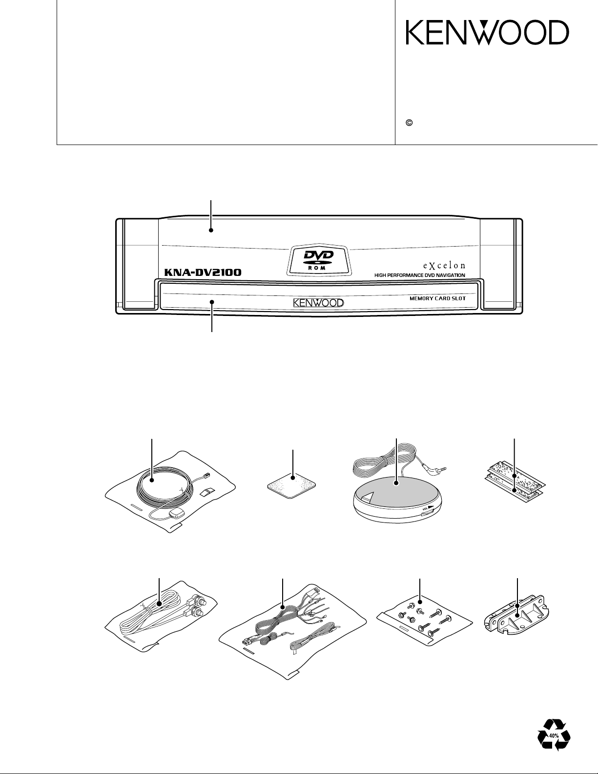
DVD NAVIGATION SYSTEM
KNA-DV2100
SERVICE MANUAL
DRESSING PANEL ASSY
(A21-4147-12)
2001-5 PRINTED IN JAPAN
B51-7807-00 (N) 1519
PUSH
DRESSING PANEL ASSY
(A21-4116-03)
ELECTRIC CIRCUIT MODULE
(W02-3261-05)
CORD ASSY
(E30-4747-05)
MOUNTING
HARDWARE
(J21-7625-04)
DC CORD ASSY
(E30-4964-05)
ELECTRIC CIRCUIT MODULE
(W02-3305-05)
SCREW SET
(N99-1713-05)
MAGIC TAPE
(H30-0514-05) x2
BRACKET
(J19-4596-04) x2
2
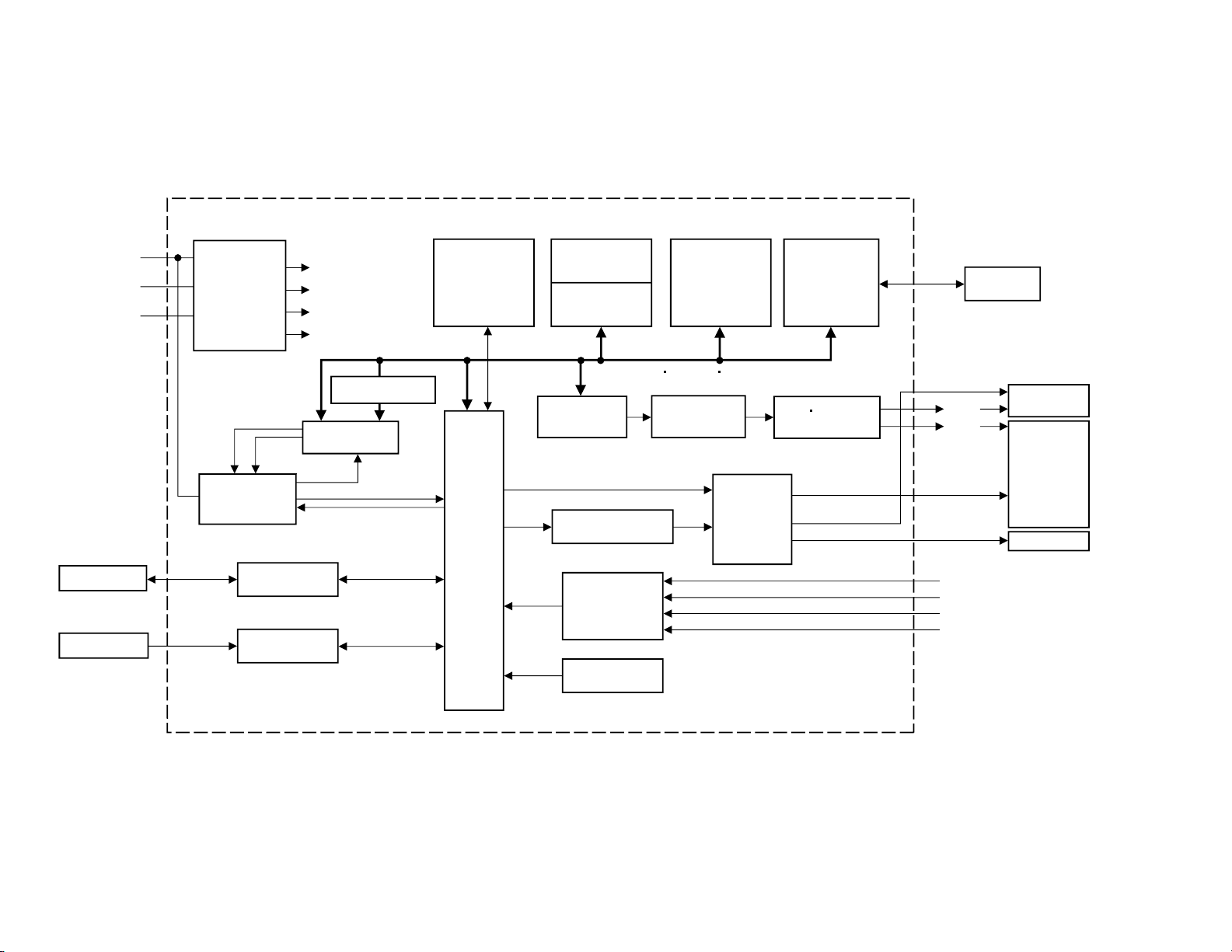
DVD
IC901,902
IC905 IC951-955,T951
IC906
MECHA.
CFC INTERFACE
POWER
SUPPLY
IC101,103,104,106,107
T101,104-111
6.7V DVD
5V
OUTSIDE INTERFACE
3.3V
INSIDE INTERFACE
1.8V
SH4
+B
ACC
GND
SDRAM
(16MBX2)
BOOTROM
(2MB)
SRAM
(512KB)
DATA ADDRESS CONTROL SIGNAL
FMU3
IC303 IC301 T507
T502-504,506,508
IC507
IC352,353
IC451,452
GY801
DAC&
NTSC ENCODER
VOICE REFLECTION
OUTPUT INTERFACE
SIGNAL CONTROL IC
IC202
IC201
STATUS0.1
SH4
T102,103
IC110
IC105
SHCKE
RESET
WDP
B.UP
NMI
IO
-PLUS
RS422
IC402,403
IC431-433,435,437
IC802,809,810
GPS MCM
GPS ANTENNA
RS422 DEVICE
GYRO
VEHICLE
INTERFACE
VOICE GUIDANCE,
VOICE OUTPUT CIRCUIT
MUTE
SWITCHING
INTERFACE
NAVI VOICE/BEEP
TV VOICE
PKB
REV
ILL
SPD
DISPLAY
REFLECTION
VOICE
MONITOR
ASP
NTSC
RGB
CFC
KNA-DV2100
BLOCK DIAGRAM
ABCD-DVD
EF-CD
ABCD-CD
LD CD
PD DVD
PD CD
LD DVD
APC
FOK
PI
CE
TE
FE
RF
CE
TE
FE
RF
SERIAL-CONT.
PI
TRACKING-DRIVE
FOCUS-DRIVE
FOCUS-JUMP
SLED-DRIVE
LOADING-CONT.
FOCUS-COIL
TRACKING-COIL
SLED-MOTOR
LOADING-MOTOR
VCC DR LD-ON
BUS
RF
CD DATA
CD-SPO
SPO
BUS
JITTER
OFFSET
JITTER-MON.
FE
SERIAL-CONT.
FZL
FZH
CD-SPO
CD-DATA
FOCUS-JUMP
LD-ON
LOADING-CONT.
MUTE
FG
EC
MUTEMUTE
FG
H-SENS
MOTOR
SPINDLE-
SENSORS
HOT
SLED-SW
PH-B
SLED-PH
PH-C
PH-A
DOWN-SW
SLED-PH
HOT
PH-C
DOWN-SW
PH-A
PH-B
SLED-SW
SENSORS
SERIAL-CONT.
EJECT
XTAL
XTAL
ATAPI I/F
6.5V
to RF-BLOCK
PROM u-COM.
POWER CONT.
PHOTO ON
PROM u-COM.
5V
to SENS.-LED to SPINDLE-DRIVER
to u-COM
EEPROM
VCC
to SERVO-IC
VDD
VDD5
to ROM-DECODER
to ROM-DECODER
to ACT.
/MOTOR
-DRIVER VM
to SPINDLE
-DRIVER
HRESET
ATA
MRESET
ATA-RST
MRESET
HRST
XRST
XRST
L-RES
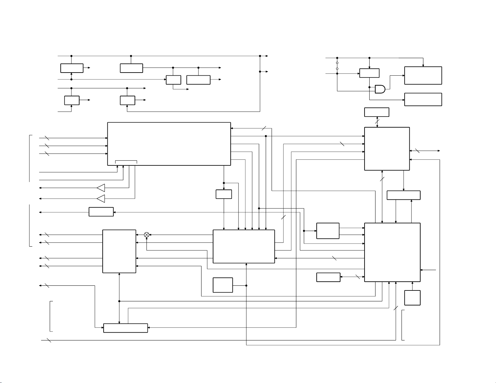
RF/MATRIX-AMP.
DISC-SERVO
CD-DSP.
FOK
ACTUATOR
-DRIVER
PICKUP
HFM-SW.
u-COM
ATAPI-IF
ROM-DECODER
D-RAM
JITTER-AMP.
DVD-DSP
FE-DET.
EEPROM
SPINDLE-DRIVER
16M
XTAL
OSC.
33.86M
5V AVR
SW. SW.
5V AVR
SW. 3V AVR
u-COM
ROM-DECORD
ATAPI-IF
DVD-DSP
CD-DSP.
SERVO
IC7
Q13,27 IC15
IC21
Q14,15 Q23,24
IC1
Q2
Q1
Q3,5
IC8
IC9
X1,IC17
IC20
IC4
IC14
IC20
IC16
IC14
IC11
IC22
IC3
IC22
IC5,6,Q6
IC23
X2
POWER LINES AND CONTROL
RESET LINES
BLOCK DIAGRAM (MECHANISM)
3
KNA-DV2100
KNA-DV2100
COMPONENTS DESCRIPTION
MAIN UNIT
Ref.No. Component Name Application/Function Operation/Condition/Compatibility
IC101 BA9743AFV Switching regulator IC DC/DC Converter voltage controller for 6.8V and 3.3V power lines
IC103 SCI7810YTA AVR IC 3.3V output
IC104 BA05FP AVR IC 5V output
IC105 TC75W56FU Comparator ACC & BU voltage detector
IC106 PQ07VZ012ZP AVR IC 1.8V output
IC107 SCI7720YFA Reset IC When momentary power down has detected, IC outputs “Lo”.
IC110 KKQ32F Reset MI-COM Reset controller for Main CPU and peripheral circuits
IC201 HD6417750F167I Main CPU (SH4)
IC202 KKQ28F Data controller Data selector of data bus
IC301 CXA2106R Video DAC+NTSC encoder
IC302 TC7SH00F NAND Clock buffer
IC303 KKQ22F Graphics controller Graphics data generator (FMU III)
IC352 UPC842G2 Op. Amp. Audio and beep signal adder and buffer
IC353 TC7W53FU Analogue SW
IC357 TC7SET08F AND Audio mute control signal generator
IC402 SN65C1168NS Line transceiver RS422 transceiver
IC403 TC74VHC00FT NAND Data buffer
IC433 TC7SU04F Inverter
IC435 TC7SU04F Inverter
IC437 TC7SU04F Inverter
IC438 UPC29L03T AVR IC 3V output
IC451 TD62604F Variable threshold driver Vehicle signals waveform shaping
IC452 TC7WU04FU Inverter Vehicle speed pulse waveform shaping
IC606 TC7SET00F NAND DVD interrupt signal buffer (3V→5V level converter)
IC701 PQ1R52 AVR IC 5.2V output
IC801 KKQ27F IO PULS Extended IO
IC802 TC7SU04F Inverter
IC809 TC7SU04F Inverter
IC810 TC7SU04F Inverter
IC901 MB81F121642102 SDRAM 128M
IC902 MB81F121642102 SDRAM 128M
IC903 TC7SH08F AND SH-CKE buffer
IC904 TC7SH00F NAND CSRAM buffer
IC905 KKQ31F BOOT ROM 2M
IC906 TC55V400FT-85 SRAM 256K
IC951 TC74LCX16245AF Bus transceiver PCMCIA I/F (Data input/output buffer)
IC952 TC74LCX32F OR PCMCIA I/F (CF card detector)
IC953 TC74LCX16244AF Bus buffer PCMCIA I/F (Address and control signals buffer)
IC954 TC7WH125FU Bus buffer PCMCIA I/F (CF card CE control)
IC955 TC74LCX138F Data decoder PCMCIA I/F (CF card input/output control decoder)
T101 2SJ327Z PON SW While ACC is applied and IC110’s P37 is “Hi”, BU is supplied throu T101.
T102 RN1404 PON SW While ACC is applied, T102 is turned on.
4
KNA-DV2100
COMPONENTS DESCRIPTION
Ref.No. Component Name Application/Function Operation/Condition/Compatibility
T103 RN1404 PON SW When IC110’s P37 becomes “Hi”, T103 is turned on.
T104 2SD1782K Driver T110 driver
T105 2SD1782K Driver T111 driver
T106 2SB1198K Driver T111 driver
T107 2SA1162
T108 2SB1301
T109 2SB1198K Driver T110 driver
T110 2SJ327Z DC/DC chopper For 6.8V AVR
T111 2SJ327Z DC/DC chopper For 3.3V AVR
T401 RN2402
T402 RN1402 When T402’s base becomes “Hi”, T401 is turned on.
T701 2SB1301 AVR driver T701 is combined with IC701, and it outouts 5.2V.
T702 2SB1301 Current limiter
T951 2SB1301 VCC3 SW CF card power supply switch
BVCC3D power supply selector
BVCC3D power supply selector
LMUTE driver
T107 is turned on during BACKUP mode.
T108 is turned on except BACKUP mode.
External LINE MUTE signal driver
SUB UNIT
Ref.No. Component Name Application/Function Operation/Condition/Compatibility
IC507 PQ1R52 AVR IC 5.2V AVR for ASP
IC508 TC74VHCT08AF AND TV monitor’s RX/TX signal buffer
IC510 TC7W53FU Signal selector Remote control signal selector of TV and external remote sensor
T501 RN1401 Audio mute SW For RCA pinjack
T502 2SC2712 Audio signal buffer For RCA pinjack
T503 RN1401 ASP mute SW For ASP
T504 2SC2712 ASP signal buffer For ASP
T505 RN1401 TV audio signal mute SW For TV monitor
T506 2SC2712 TV audio signal buffer For TV monitor
T507 2SA1162 SYNC signal buffer For TV monitor
T508 RN1402 Mute SW driver For audio signal muting
SUB-CIRCUIT UNIT (X13-9770-00)
Ref.No. Component Name Application/Function Operation/Condition/Compatibility
IC1 NJM2406F Comparator Sled pulse waveform shaping
DVD UNIT (X37-1010-01)
Ref.No. Component Name Application/Function Operation/Condition/Compatibility
IC1 SP3721A RF signal processor IC
IC2 NJM2125F Op.amp. VC (2.5V) buffer
IC3 NJU7093A Op.amp. Jitter signal amplifier
IC4 NJM2406F Comparator FOK signal generator (PI comparator)
IC5 NJM2100M Op.amp. Layer jump monitor (FE signal invert, LPF)
IC6 LA6393M Comparator Layer jump monitor (Window comparator)
RF signal processor (AGC, EQ and etc.), servo signal processor (FE,
TE, CE, DFCT ,MIRR, APC and etc.)
5
KNA-DV2100
COMPONENTS DESCRIPTION
Ref.No. Component Name Application/Function Operation/Condition/Compatibility
IC7 L88MS05T 5V AVR IC 5V output for RF amplifier, pickup and servo circuits
IC8 LA6563 4ch BTL driver Focusing coil, tracking coil, sled motor and lording motor driver
IC9 BD6661FV 3 phase motor driver PWM driving
IC10 NJU7096AR Op.amp. Spindle servo signal amplifier (LPF, gain matching)
IC11 SN74AHC1G08D AND IC14 reset controler
IC12 NJM2125F Op.amp. VC2 (1.65V) buffer
IC13 SN74AHC1G08D AND IC20 clock on/off gate
IC14 CXD1867R Data decoder IC
IC15 L88M33T AVR IC 3.3V output for IC14
IC16 IS41C16256 DRAM EDO DRAM 4M
IC17 SN74AHC2GU04H Inverter Clock oscilator for IC14 and IC20, and buffer (33.86MHz)
IC19 SN74AHC1GU04D Inverter “HRES–” inverter
IC20 CXD3008Q Digital signal processor IC
IC21 L88MS05T AVR IC 5V output for IC14, IC20 and digital circuits
IC22 HD6433062G24XI Mechanism control MI-COM.
IC23 BR24C04FV-W EEPROM Data backup memory (coefficient and others)
Q1 MCH6101 DVD APC DVD laser power control
Q2 MCH6101 CD APC CD laser power control
Q3 2SB1295 DVD laser high-frequency When Q5’s base becomes “Hi”, Q3 is turned on and DVD laser high-
Q5 DTC124EUA redundancy circuit SW frequency redundancy circuit is working.
Q4 3LN01M DFT level converter
Q6 3LP01M Layer jump monitor
Q7 DTC124EUA Layer gain select SW When a base becomes “Hi”, Q7 is turned on and sets the gain to Lo.
Q8 2SB1295 Sled movement detection When Q9’s base becomes “Hi”, Q8 is turned on and 5V power supply is
Q9 DTC124EUA circuit on/off SW supplied.
Q10 2SC4081 Layer jump control SW For Lo kicking
Q11 2SA1576A
Q12 2SC4081 When Q12’s base becomes “Hi”, Q11 is turned on.
Q13 DTC124EUA
Q27 CPH3105
Q14 2SB1295
Q15 DTC124EUA
Q16 3LP01M FDCHG inverter FDCHG logic reversal
Q17 DTC124EUA HRES- inverter
Q18 DTC124EUA IC7 power supply SW When a base becomes “Hi”, Q18 is tur ned on and AVR is working.
Q23 DTC124EUA
Q24 2SB1295
Q25 3LN01M MIRR level conversion
Q26 UMC2N IFSEL SW When a base becomes “Hi”, Q26 is turned on.
Layer jump control SW
IC20 power supply SW When Q13’s base becomes “Hi”, Q27 is turned on.
Disc detection circuit SW When Q15’s base becomes “Hi”, Q14 is turned on.
IC9 VCC SW When Q23’s base becomes “Hi”, Q24 is turned on and IC9 is working.
CD-ROM/DVD data decoder, ATAPI I/F, AV decoder I/F, DVD PLL, DVD
error collection, Buffered Audio Play, Subcode data
CD PLL, CD error corection operation, digital servo (focusing, tracking,
and sled) function, automatic adjustment
For Hi kicking
6
KNA-DV2100
MICROCOMPUTER’S TERMINAL DESCRIPTION
IC110 : MAIN UNIT
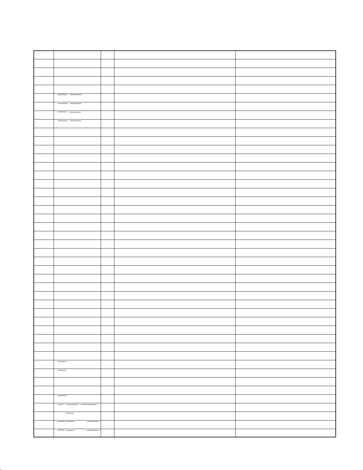
Pin No. Pin Name I/O Description Processing Operation
1 P04 (TEL-CGON) O Power supply circuit control output Hi : Power supply circuit ON
2 P05 (TEL-CHAG) I Power supply circuit ON request input Hi : Start request
3 P06 (ACC ON) O ACC ON output to IO PLUS Lo : ACC ON
4 P07 (B UP) O Backup condition set-up output Lo : Backup condition
5 MODE0 - Not used (connected to GND lines)
6 MODE1 - Not used (connected to GND lines)
7 RST I
8 XO O Resonator connection terminal
9 XI I Resonator connection terminal
10 VSS - GND connection terminal Connected to GND lines.
11 P37 (POWER ON) O P ON output Hi : Power ON
12 P36 (WDP) I WDP input Detection of pulse edge
13 P35 (ACC) I ACC detection input Hi : ACC ON
14 P34 (BU) I Momentary power down detection Hi : BU ON
15 P33 (CKE) I CKE from SH4
16 C - Capacitor connection terminal
17 P32 (IOPFLWR) O Not used (N.C.)
18 P31 (ST1) I Status input 1 from SH4
19 P30 (ST0) I Status input 0 from SH4
20 P50 (IORES) O IO PLUS reset output Lo : Reset
21 AVSS - GND connection terminal Connected to GND lines.
22 P40 (VCC3ON) O VCC3D selection terminal (Normal) Lo : Normal operation
23 P41 (BVC3ON) O VCC3D selection terminal (Backup) Lo : Backup mode
24 P42 (RMUTE) O Mute output at Power ON/OFF Lo : Mute ON
25 P43 (RES3) O NAVI reset output (VCC3 system reset signal) Lo : Reset
26 P00 (SH4NMI) O NMI output to SH4 Hi→Lo : Back up request to SH4
27 P01 (TEL-OVER) I Output voltage watch of power supply circuit Lo : Output imprudence
28 P02 (6.8VDET) I Output voltage watch of 6.8V power line (CDHVCC) Hi : Output voltage OK
29 P03 (3.3VDET) I Output voltage watch of 3.3V power line (VCC3) Hi : Output voltage OK
30 VCC - Positive power supply connection terminal Connected to Backup power supply.
RESET input (connected with RESET SW on the panel)
Lo : Reset
Lo : SDRAM self-refresh,
Hi : SDRAM normal operation
IC201 : MAIN UNIT
Pin No. Pin Name I/O Description Processing Operation
1 RDY I RDY input
2 RESET I Reset input Lo : Reset
3 CS0 O Chip select 0 output Lo : Selected (BOOT ROM)
4 CS1 O Chip select 1 output Lo : Selected (SRAM)
5 CS4 O Chip select 4 output Lo : Selected (IO PLUS)
6 CS5 O Chip select 5 output Not used (N.C.)
7 CS6 O Chip select 6 output Lo : Selected (CF Card)
8 BS O Bus start
9 VDDQ - Positive power supply connection terminal (+3.3V) Connected to VCC3 lines.
7
KNA-DV2100
MICROCOMPUTER’S TERMINAL DESCRIPTION
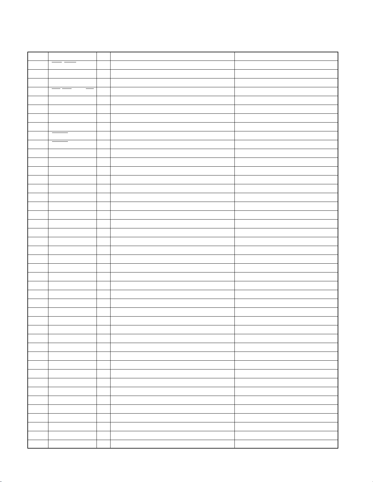
Pin No. Pin Name I/O Description Processing Operation
10 VSSQ - GND connection terminal Connected to GND lines.
11 D47 I/O Data bus Not used (N.C.)
12 D32 I/O Data bus Not used (N.C.)
13 VDD - Positive power supply connection terminal (+1.8V) Connected to VCC1.8 lines.
14 VSS - GND connection terminal Connected to GND lines.
15 D46 I/O Data bus Not used (N.C.)
16 D33 I/O Data bus Not used (N.C.)
17 D45 I/O Data bus Not used (N.C.)
18 D34 I/O Data bus Not used (N.C.)
19 D44 I/O Data bus Not used (N.C.)
20 D35 I/O Data bus Not used (N.C.)
21 VDDQ - Positive power supply connection terminal (+3.3V) Connected to VCC3 lines.
22 VSSQ - GND connection terminal Connected to GND lines.
23 D43 I/O Data bus Not used (N.C.)
24 D36 I/O Data bus Not used (N.C.)
25 D42 I/O Data bus Not used (N.C.)
26 D37 I/O Data bus Not used (N.C.)
27 D41 I/O Data bus Not used (N.C.)
28 D38 I/O Data bus Not used (N.C.)
29 D40 I/O Data bus Not used (N.C.)
30 D39 I/O Data bus Not used (N.C.)
31 VDDQ - Positive power supply connection terminal (+3.3V) Connected to VCC3 lines.
32 VSSQ - GND connection terminal Connected to GND lines.
33 D15 I/O Data bus
34 D0 I/O Data bus
35 D14 I/O Data bus
36 D1 I/O Data bus
37 D13 I/O Data bus
38 D2 I/O Data bus
39 VDD - Positive power supply connection terminal (+1.8V) Connected to VCC1.8 lines.
40 VSS - GND connection terminal Connected to GND lines.
41 D12 I/O Data bus
42 D3 I/O Data bus
43 VDDQ - Positive power supply connection terminal (+3.3V) Connected to VCC3 lines.
44 VSSQ - GND connection terminal Connected to GND lines.
45 D11 I/O Data bus
46 D4 I/O Data bus
47 D10 I/O Data bus
48 D5 I/O Data bus
49 D9 I/O Data bus
50 D6 I/O Data bus
51 BACK/BSREQ O Bus use permission output
52 BREQ/BSACK I Bus release request input
53 D8 I/O Data bus
8
KNA-DV2100
MICROCOMPUTER’S TERMINAL DESCRIPTION
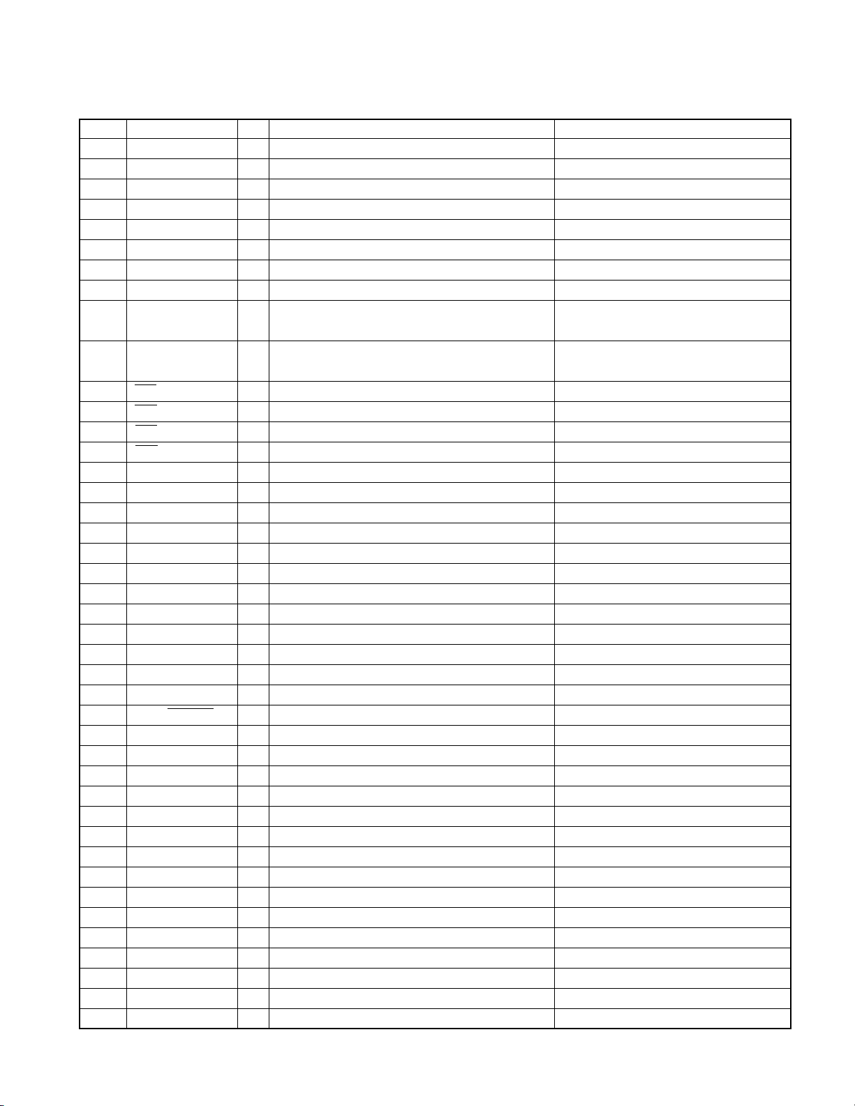
Pin No. Pin Name I/O Description Processing Operation
54 D7 I/O Data bus
55 CKE O Clock enable
56 VDDQ - Positive power supply connection terminal (+3.3V) Connected to VCC3 lines.
57 VSSQ - GND connection terminal Connected to GND lines.
58 WE5/CAS5/DQM5 O Not used (N.C.)
59 WE4/CAS4/DQM4 O Not used (N.C.)
60 WE1/CAS1/DQM1 O D15~D0 choice output
61 WE0/CAS0/ DQM0 O D15~D0 choice output
62 A17 O Address bus
63 A16 O Address bus
64 A15 O Address bus
65 VDD - Positive power supply connection terminal (+1.8V) Connected to VCC1.8 lines.
66 VSS - GND connection terminal Connected to GND lines.
67 A14 O Address bus
68 A13 O Address bus
69 VDDQ - Positive power supply connection terminal (+3.3V) Connected to VCC3 lines.
70 VSSQ - GND connection terminal Connected to GND lines.
71 A12 O Address bus
72 A11 O Address bus
73 A10 O Address bus
74 A9 O Address bus
75 A8 O Address bus
76 A7 O Address bus
77 CKIO O Clock output
78 VDDQ - Positive power supply connection terminal (+3.3V) Connected to VCC3 lines.
79 VSSQ - GND connection terminal Connected to GND lines.
80 A6 O Address bus
81 A5 O Address bus
82 A4 O Address bus
83 A3 O Address bus
84 A2 O Address bus
85 DRAK1 O Not used (N.C.)
86 DRAK0 O Not used (N.C.)
87 VDDQ - Positive power supply connection terminal (+3.3V) Connected to VCC3 lines.
88 VSSQ - GND connection terminal Connected to GND lines.
89 CS3 O Chip select 3 output Lo : Selected (SDRAM)
90 CS2 O Chip select 2 output Not used (N.C.)
91 VDD - Positive power supply connection terminal (+1.8V) Connected to VCC1.8 lines.
92 VSS - GND connection terminal Connected to GND lines.
93 RAS O SDRAM RAS control output
94 RD/CASS/FRAME O SDRAM CAS control output
95 RD/WR O Read/Write control output
96
97
WE2/CAS2/DQM2/ICIORD
WE3/CAS3/DQM3/ICIOWR
O D31~D16 choice output
O D31~D16 choice output
9
KNA-DV2100
MICROCOMPUTER’S TERMINAL DESCRIPTION
Pin No. Pin Name I/O Description Processing Operation
98 WE6/CAS6/DQM6 O Not used (N.C.)
99 VDDQ - Positive power supply connection terminal (+3.3V) Connected to VCC3 lines.
100 VSSQ - GND connection terminal Connected to GND lines.
101
102 D23 I/O Data bus
103 D24 I/O Data bus
104 D22 I/O Data bus
105 RXD I Not used (N.C.)
106 DREQ0 I Not used (pull up to VCC3 lines)
107 DREQ1 I Not used (pull up to VCC3 lines)
108 D25 I/O Data bus
109 D21 I/O Data bus
110 D26 I/O Data bus
111 D20 I/O Data bus
112 D27 I/O Data bus
113 VDDQ - Positive power supply connection terminal (+3.3V) Connected to VCC3 lines.
114 VSSQ - GND connection terminal Connected to GND lines.
115 D19 I/O Data bus
116 D28 I/O Data bus
117 VDD - Positive power supply connection terminal (+1.8V) Connected to VCC1.8 lines.
118 VSS - GND connection terminal Connected to GND lines.
119 D18 I/O Data bus
120 D29 I/O Data bus
121 D17 I/O Data bus
122 D30 I/O Data bus
123 D16 I/O Data bus
124 D31 I/O Data bus
125 VDDQ - Positive power supply connection terminal (+3.3V) Connected to VCC3 lines.
126 VSSQ - GND connection terminal Connected to GND lines.
127 D55 I/O Data bus Not used (N.C.)
128 D56 I/O Data bus Not used (N.C.)
129 D54 I/O Data bus Not used (N.C.)
130 D57 I/O Data bus Not used (N.C.)
131 D53 I/O Data bus Not used (N.C.)
132 D58 I/O Data bus Not used (N.C.)
133 D52 I/O Data bus Not used (N.C.)
134 D59 I/O Data bus Not used (N.C.)
135 VDDQ - Positive power supply connection terminal (+3.3V) Connected to VCC3 lines.
136 VSSQ - GND connection terminal Connected to GND lines.
137 D51 I/O Data bus Not used (N.C.)
138 D60 I/O Data bus Not used (N.C.)
139 D50 I/O Data bus Not used (N.C.)
140 D61 I/O Data bus Not used (N.C.)
141 D49 I/O Data bus Not used (N.C.)
WE7/CAS7/DQM7/REG
O Not used (N.C.)
10
KNA-DV2100
MICROCOMPUTER’S TERMINAL DESCRIPTION
Pin No. Pin Name I/O Description Processing Operation
142 D62 I/O Data bus Not used (N.C.)
143 VDD - Positive power supply connection terminal (+1.8V) Connected to VCC1.8 lines.
144 VSS - GND connection terminal Connected to GND lines.
145 D48 I/O Data bus Not used (N.C.)
146 D63 I/O Data bus Not used (N.C.)
147 VDDQ - Positive power supply connection terminal (+3.3V) Connected to VCC3 lines.
148 VSSQ - GND connection terminal Connected to GND lines.
149 MD0/SCK I/O Clock movement matter mode selection terminal Pull up to VCC3 Lines.
150 MD1/TXD2 I/O
151 MD2/RXD2 I
152 IRL0 I Interrupt input 0
153 IRL1 I Interrupt input 1
154 IRL2 I Interrupt input 2
155 IRL3 I Interrupt input 3
156 NMl I NMl interrupt input
157 XTAL2 O Not used (N.C.)
158 EXTAL2 I Not used (connected to VCC3 lines)
159 VSS · RTC - GND connection terminal Connected to GND lines.
160 VDD · RTC (3.3V) - Positive power supply connection terminal (+3.3V) Connected to VCC3 lines.
161 RESERVED I Not used (connected to VCC3 lines)
162 VSS - GND connection terminal Connected to GND lines.
163 VDDQ - Positive power supply connection terminal (+3.3V) Connected to VCC3 lines.
164 CTS2 I/O Not used (pull up to VCC3 lines)
165 TCLK I/O Not used (pull up to VCC3 lines)
166 MD8/RST2 I/O Crystal resonator settlement terminal Pull up to VCC3 lines.
167 MD7/TXD I/O Master mode settlement terminal Pull up to VCC3 lines.
168 SCK2/MRESET I Not used (pull up to VCC3 lines)
169 VDD - Positive power supply connection terminal (+1.8V) Connected to VCC1.8 lines.
170 VSS - GND connection terminal Connected to GND lines.
171 A18 O Address bus
172 A19 O Address bus
173 A20 O Address bus
174 A21 O Address bus
175 A22 O Address bus
176 A23 O Address bus
177 VDDQ - Positive power supply connection terminal (+3.3V) Connected to VCC3 lines.
178 VSSQ - GND connection terminal Connected to GND lines.
179 A24 O Address bus
180 A25 O Address bus
181 MD3/CE2A I/O Area 0 bus width settlement terminal Pull down to GND lines.
182 MD4/CE2B I/O Area 0 bus width settlement terminal Pull up to VCC3 lines.
183 MD5/RAS2 I/O Pull down to GND lines.
Clock movement matter mode selection Pull up to VCC3 Lines/Communication
terminal/Communication output to TV monitor output to TV monitor
Clock movement matter mode selection Pull up to VCC3 Lines/Communication
terminal/Communication input from TV monitor input from TV monitor
11
KNA-DV2100
MICROCOMPUTER’S TERMINAL DESCRIPTION
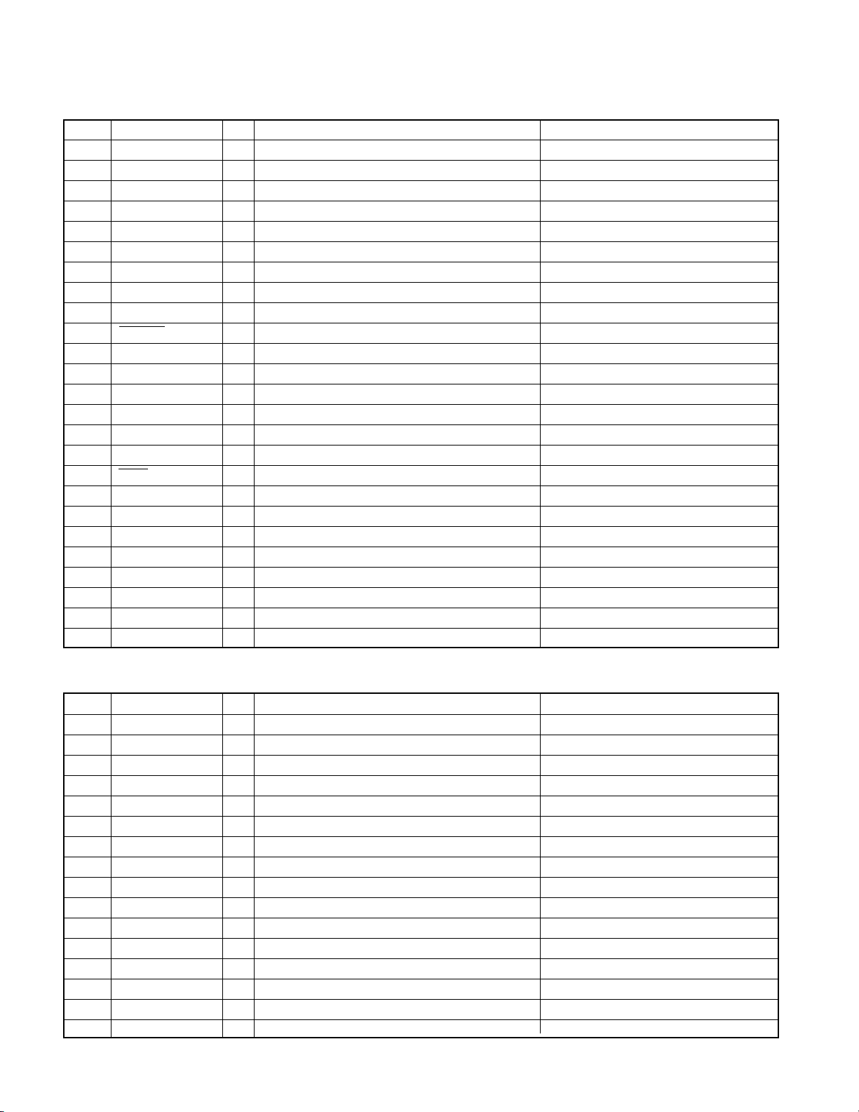
Pin No. Pin Name I/O Description Processing Operation
184 DACK0 O Not used (N.C.)
185 DACK1 O Not used (N.C.)
186 A0 O Address bus Not used (N.C.)
187 VDDQ - Positive power supply connection terminal (+3.3V) Connected to VCC3 lines.
188 VSSQ - GND connection terminal Connected to GND lines.
189 A1 O Address bus
190 STATUS0 O CPU status output 0
191 STATUS1 O CPU status output 1
192 MD6/IOIS16 I Area 0 bus normal settlement terminal Pull up to VCC3 lines.
193 ASEBRK/BRKACK I/O Emulator special terminal (UDI) Connected to the test pin (CN150).
194 TDO O Data output terminal (UDI) Connected to the test pin (CN150).
195 VDD - Positive power supply connection terminal (+3.3V) Connected to VCC3 lines.
196 VSS - GND connection terminal Connected to GND lines.
197 TMS I Mode selection input terminal (UDI) Connected to the test pin (CN150).
198 TCK I Serial clock input terminal (UDl) Connected to the test pin (CN150).
199 TDI I Data input terminal (UDl) Connected to the test pin (CN150).
200 TRST I Reset input terminal (UDl) Connected to the test pin (CN150).
201 VDD-PLL2 - PLL2 positive power supply connection terminal Connected up to VCC3 lines.
202 VSS-PLL2 - GND connection terminal Connected to GND lines.
203 VDD-PLL1 - PLL1 positive power supply connection terminal Connected up to VCC3 lines.
204 VSS-PLL1 - GND connection terminal Connected to GND lines.
205 VDD-CPG - PG positive power supply connection terminal Connected up to VCC3 lines.
206 VSS-CPG - GND connection terminal Connected to GND lines.
207 XTAL I Crystal resonator connection terminal Frequency : 19.8MHz
208 EXTAL O Crystal resonator connection terminal
IC22 : DVD UNIT (X37-1010-01)
Pin No. Pin Name I/O Description Processing Operation
1 VCC - Positive power supply connection terminal Connected up to 5V lines.
2 DATA O Serial data output to CXD3008Q
3 XLAT O Serial data latch output to CXD3008Q
4 CE O Chip selection output to CXD1867R Lo : Selected
5 SCLK O SENS data clock output to CXD3008Q
6 F REQ O Local I/F RDY output
7 E2 CLK I/O EEPROM clock output
8 E2 DATA I/O EEPROM data input/output
9 PON O RF5V,D5V ON/OFF control Hi : ON, Lo : OFF
10 FWE I Flash memory writing input Not used (pull down to GND lines)
11 VSS - GND connection terminal Connected to GND lines.
12 F DATA O Local I/F data transmission output
13 GAIN O Pickup gain selection output Hi : Gain set-up Lo
14 B DATA I Local I/F data reception input
15 RXD1 I Not used (pull up to 5V lines)
16 B CLK I Local I/F clock input
12
 Loading...