

CD RECEIVER
KDC-4047UA/UG/UGY/UM
KDC-414UA /414UM
KDC-MP245U
KDC-U3046/U346/U4046
SERVICE MANUAL
© 2009-11 PRINTED IN JA PAN
B53-0767-10 (N) 341
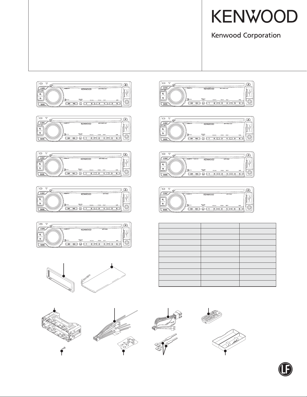
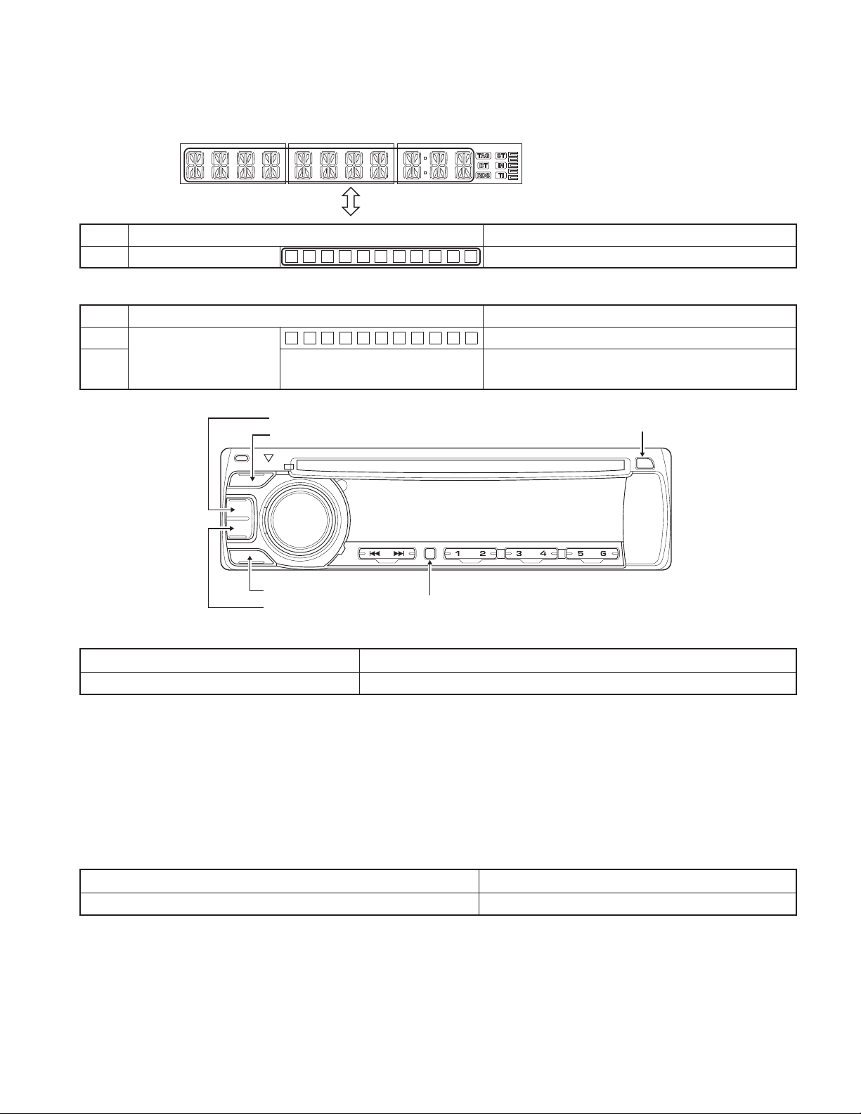
KDC-4047UA/UG : Panel assy (A64-5002-12)
KDC-4047U
KDC-4047UM : Panel assy (A64-5131-12)
KDC-4047UM
KDC-414UM : Panel assy (A64-5132-12)
KDC-414UM
KDC-U3046 : Panel assy (A64-5008-12)
KDC-U3046
KDC-U4046 : Panel assy (A64-5016-12)
KDC-U4046
Escutcheon
(B07-3270-01)
* Carrying case
(W01-1710-05)
KDC-4047UGY : Panel assy (A64-5004-12)
KDC-4047UGY
KDC-414UA : Panel assy (A64-5003-12)
KDC-414U
KDC-MP245U : Panel assy (A64-5001-12)
KDC-MP245U
KDC-U346 : Panel assy (A64-5009-12)
KDC-U346
TDF SPARE-PANEL
MAIN UNIT NAME
KDC-4047UA Y33-3242-73 TDF-4047UA
KDC-4047UG Y33-3242-74 TDF-4047UG
KDC-4047UGY Y33-3242-76 TDF-4047UGY
KDC-4047UM Y33-3250-23 TDF-4047UM
KDC-414UA Y33-3242-75 TDF-414UA
KDC-414UM Y33-3250-24 TDF-414UM
KDC-MP245U Y33-3240-11 TDF-MP02DU
KDC-U3046 Y33-3250-21 TDF-U3046
KDC-U346 Y33-3250-22 TDF-U346
KDC-U4046 Y33-3253-02 TDF-U4046
TDF PARTS No.
TDF NAME
Mounting hardware assy
(J22-0789-03)
* Screw (4x16)
(N84-4016-48)
* Depends on the model. Refer to the parts list.
* DC cord
(E30-xxxx-xx)
* Screw set
(N99-1757-15)
* DC cord
(E30-xxxx-xx)
Lever
(D10-7106-04) x2
This product complies with the
* Remote controller assy (RC-405)
(A70-2104-05)
* Plastic cabinet assy
(A02-2755-23)
This product uses Lead Free solder.
RoHS directive for the European market.
KDC-4047UA/4047UG/4047UGY/4047UM
KDC-414UA /414UM/MP245U/U3046/U346/U4046
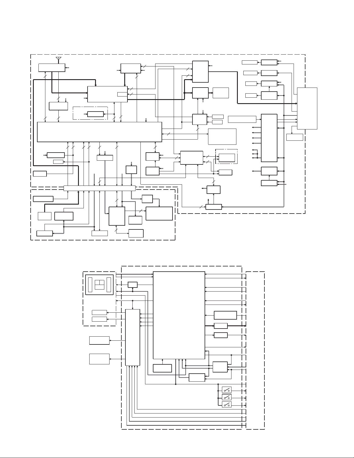
BLOCK DIAGRAM
ELECTRIC UNIT (X34-660x-xx)
IC501
TUNER ATOMIC
3
3
IC1
BU5V
S3
RESET
PANEL DET
J2
FRONT
AUX
∗
IC2
REMOTE
ANT.
A8V
SW5V
1
∗
IC7
RDS
DECODER
IC8
ROM CORRECTION (NOT USED)
3
12
RESET IC
DC CN
J3
J1
to GND
S1
ROTARY
ENCODER DRIVER
SWITCH UNIT (X16-675x-xx)
A8V
SERVO+B
IC2
E-VOL
IC10
E2PROMSW5V
SYSTEM u-COM
111
BU5V
PANEL5V
USB5V
2
CONNECTOR
PANEL5V
J3
USB CN
Q301
IC1
ACC-DET
BU-DET
P-STBY
FL+B
A8V
D5V
R118
Q101
ACC-DET
Q103
Q102
IC4
POWER
SUPPLY
IC
Q2,3
Q11,12
PHONE
BU-DET
SURGE
-DET
CD
SERVO
SW14V
SW5V
BU5V
to SYSTEM
u-COM (IC1)
SW5V
J1
DC-CN
PHONE
SP-OUT
FRONT L/R
REAR L/R
ACC
B.U.
P-ANT
P-CON
OEM REMOTE
IC900
8
Bolero u-COM
(SUB u-COM)
2
1
∗
Q707
IC6
POWER
IC
∗
Q703-706
PRE
MUTE
MUTE
1
USB5V
BU5V
BU5V
J1,IC4
DC-CN etc
PHONE
ACC-DET / BU-DET
PS1-1 / PS1-2 / PS1-3
PS2-1
2
4
HI-SIDE
SW
FL+B
2
USB5V
BU
∗
J5
PRE-OUT
FRONT
REAR/SW
BU-DET
RESET
(NOT USED)
∗
2
IC52
IC51
PS1-1 / PS1-2 / PS1-3
PS2-1 / PS2-2
IC951
Bolero
E2PROM
IC950
iPod IC
LINE MUTE
ILLUMI+B
SW5V
SW5V
BU5V
SERVO+B
DME1
CD MECHA
(X32- )
MUTE
1
2
5
ILLUMI+B
5
FL
9
R15
1
1
1/2W
Rx1
KEY
ILLUMI
KEY
MATRIX
5
FL+B
15
BU5V
BU5V
8
IC251,
252
LEVEL
SHIFT
IC53
BU3.3V
R31
FL+B
1/2W
Rx1
FL DISPLAY
(13-SEG, 11-DIGIT)
9
BU5V
BU5V
ED1
DPU1
ACB
EF
FO COIL
TR COIL
DM1
SPINDLE
MOTOR
DM2
LOADING &
SLED
MOTOR
CD PLAYER UNIT (X32-6250-00)
IC4
SIGNAL A/B/C/E/F
Q1
APC
IC3
FO OUT
TR OUT
MOTOR
DRIVER
DM OUT
FM OUT
PD
LD
VREF
FO OUT
TR OUT
DM OUT
FM OUT
X1
CLOCK
16.934MHz
RF AMP
+
SERVO
PROCESSOR
+
MP3 DECODER
+
WMA DECODER
+
AAC DECODER
+
1M bit SRAM
D GND
BU1.5V
D1.5V
D3.3V
SRAM STB
SO
SI
BUCK
CCE
PIO0
R15
MRST MRST
ZDET MUTE L/R
A3.3V
AGND
Q14
D1.5V
OUTPUT
LEVEL SHIFT
RESISTOR
C43
Lch Lch
FILTER
C44
Rch
FILTER
IC5
BU1.5V/
D3.3V
REG
S1
S2
MOTHER
BOARD
(X34- )
SRAM STB
SO
SI
BUCK
CCE
PIO0
Rch
A.GND
BU5V
P.ON
D.GND
LOS-SW
12EJE-SW
LOE-SW
DRV MUTE
LO/EJ
MOTOR
S7.5V
S.GND
2
KDC-4047UA/4047UG/4047UGY/4047UM
KDC-414UA /414UM/MP245U/U3046/U346/U4046
COMPONENTS DESCRIPTION
SWITCH UNIT (X16-675x-xx)
●
Ref. No. Application / Function Operation / Condition / Compatibility
IC1 VFD Driver
IC2 Remote Control Sensor
ELECTRIC UNIT (X34-660x-xx)
●
Ref. No. Application / Function Operation / Condition / Compatibility
IC1 System μ-COM Controls FM/AM tuner, CD mechanism, panel, volume and tone.
IC2 E-VOL Controls the source, volume, tone.
IC4 Power Supply IC Outputs 5Vx2, 8.3V, 10.2V, P-CON, P-ANT.
IC6 Power IC Amplifi es the front L/R and the rear L/R to 50W maximum.
IC7 RDS IC RDS decoder.
IC8 Reset IC Lo when detection voltage goes below 3.6V.
IC10 E2PROM Tuner setting memory. (Not used)
IC51 USB+5V Power supply for D+5.1V. (to USB and panel)
IC52 Hi-side SW Detects USB over current.
IC53 D+3.3V AVR IC Power supply for D+3.3V.
IC251 Level Shift (3.3V → 5V) Logic IC.
IC252 Level Shift (5V → 3.3V) Logic IC.
IC501 Tuner IC (ATomIC) Tuner IC.
IC900 Bolero μ-COM USB/CD mechanism control.
IC951 Bolero E2PROM (Not used)
Q2,3 Servo+B AVR When Q3’s base goes Hi, AVR outputs 7.5V.
Q11,12 CONT SW for Servo+B ON when the base goes Hi.
Q13 CONT SW for IC4 ON when the base goes Hi.
Q14 CONT SW for IC4 ON when the base goes Lo.
Q53 FREQ CONT SW for IC51
Q101 ACC DET ON when the base goes Hi during ACC is applied.
Q102 Surge DET When the base goes Hi, surge voltage is detected.
Q103 BU DET ON when the base goes Hi during BU is applied.
Q104,105 Mute CONT ON when the base goes Hi.
Q301 Panel 5V SW ON when the base goes Lo.
Q705,706 Pre-out Mute SW When a base goes Hi, pre-out is muted.
Q707 Mute Driver for Pre-out ON when the base goes Lo.
Q902,903 3.3V AVR for IC900 When base of Q902 is Hi, 3.3V is ON.
Q905 CD “LOE LIM SW” Buffer When base of Q905 is Hi, loadingnd end completes.
When the base goes Lo, switching frequency becomes 1.3MHz.
When the base goes Hi, switching frequency becomes 1.8MHz.
3
KDC-4047UA/4047UG/4047UGY/4047UM
KDC-414UA /414UM/MP245U/U3046/U346/U4046
COMPONENTS DESCRIPTION
CD PLAYER UNIT (X32-6250-00)
●
Ref. No. Application / Function Operation / Condition / Compatibility
IC3 4ch BTL Driver
IC4 Servo DSP with built-in Audio DAC With built-in MP3/WMA/ACC decoder and 1M-bit-SRAM.
IC5 BU1.5V/D3.3V REG.
Q1 APC (Auto Power Control) Drives LD (Laser Diode).
Q14 D1.5V Output
D2 Laser Diode Protection
D3,4 Static Electricity Countermeasure Prevents malfunction by static electricity.
Driver for focusing & tracking coil, driver for sled & spindle motor, and operation for disc
loading & ejection.
Power supply for BU1.5V.
Power supply for digital/analogue/audio 3.3V.
Switches ON/OFF at one end of BU1.5V line which is separated into 2 directions.
Uses output voltage as D1.5V.
Prevents reverse bias which is applied to laser.
Laser destruction prevention.
MICROCOMPUTER’S TERMINAL DESCRIPTION
SYSTEM μ-COM : IC1 on X34- (ELECTRIC UNIT)
●
Pin No. Pin Name I/O Application
1~5 NC - Not used Output L fi xed
6 REMO I Remote control signal input Detects pulse width
7 NC - Not used Output L fi xed
8 BYTE I Memory extension bus width setting Connects to VSS
9 CNVSS - Connects to VSS
10 XCIN - 32.768kHz
11 XCOUT - 32.768kHz
12 RESET
13 XOUT - 16.0MHz
14 VSS -
15 XIN - 16.0MHz
16 VCC1 -
17 NC - Not used Output L fi xed
18 PANEL DET
19~24 NC - Not used Output L fi xed
25 PON FL O Key illumination power supply control ON: H, OFF: L
26 PON PANEL
27 NC - Not used Output L fi xed
28 BEEP O Beep output 2kHz / 1kHz
29 TUN SCL I/O Tuner I2C clock output
30 TUN SDA I/O Tuner I2C data input/output
- L: Reset
I Panel communication detection H: No panel, L: Panel detached
I/O Panel 5V control
Truth Value
Table
Processing / Operation / Description
ON: L, 11 minutes after momentary power-down or
panel detached or ACC OFF: Hi-Z
4
KDC-4047UA/4047UG/4047UGY/4047UM
KDC-414UA /414UM/MP245U/U3046/U346/U4046
MICROCOMPUTER’S TERMINAL DESCRIPTION
Pin No. Pin Name I/O Application
31 VFD SYS DATA O VFD data output
32 VFD PAN DATA I VFD data input
33 VFD CLK O VFD clock output 125kHz
34 VFD BLK O VFD driver reset output
35 S SYS DATA O Bolero serial output
36 S SOC DATA I Bolero serial input
37 S SOC CLK I Bolero serial clock input
38 CD LOS SW I CD loading detection
39
40 CD LOEJ I/O CD motor control
41 ROMCOR DET I E2PROM writing request H: Writing
41 EPM I Flash ROM EPM input
42 CD MOTOR I/O CD motor control
43 NC - Not used Output L fi xed
44 CD DISC12 SW I 12cm disc detection
45 NC - Not used Output L fi xed
46 VFD CE O VFD control request H: Possible to transfer VFD data
47 AUD SDA I/O E-VOL data input/output
48 AUD SCL I/O E-VOL clock output
49 ROTARY CCW I VOL encoder input Detects pulse width
50 ROTARY CW I VOL encoder input Detects pulse width
51 RDS DATA I/O RDS decoder data input
52 RDS QUAL I RDS decoder qualifi cation input
53 SOC MUTE I CD mute request H: Normal, L: Mute request
54 S SOC REQ
55 SOC RST O SOC reset H: Normal, L: Reset
56 SOC S STOP O SOC stop H: Normal, L: SOC stopped
57 S SYS REQ O
58~61 NC - Not used Output L fi xed
62 VCC2 -
63 NC - Not used Output L fi xed
64 VSS -
65~73 NC - Not used Output L fi xed
74 RDS CLK I/O RDS decoder clock input
75 NC - Not used Output L fi xed
76 PWIC STBY O Power IC standby control POWER ON: H, POWER OFF: L
CD LOE LIM SW
I CD detection (Chucking SW) H: Loading completed, L: No disc
I
Communication request from SOC to system μ-com
Communication request from system μ-com
to system μ-com to SOC
Truth Value
Table
q
q
Processing / Operation / Description
VFD data output. VFD_BLK (Pin34) is made Hi and
the communication begins after 500ms.
H: Reset cancelled, L: Reset,
11 minutes after momentary power-down or panel
detached or ACC OFF: L
Refer to the truth value table
L: Rewritable (Only when fl ash ROM is used).
Connects to VSS.
Refer to the truth value table
5
KDC-4047UA/4047UG/4047UGY/4047UM
KDC-414UA /414UM/MP245U/U3046/U346/U4046
MICROCOMPUTER’S TERMINAL DESCRIPTION
Pin No. Pin Name I/O Application
77 PWIC MUTE O Power IC mute
78 MUTE I/O Mute L: Mute OFF, Hi-Z: Mute ON
79 BU DET
80 ACC DET
81 TYPE1 I Destination SW Refer to the truth value table
82 TYPE2 I Destination SW Refer to the truth value table
83 NC - Not used Output L fi xed
84 PWIC DC ERR I
85 LINE MUTE I Line mute setection TEL mute: Below 1V, NAVI mute: Over 2.5V
86 TUN SMETER I S-meter input
87 PON SWREG O SW-REG ON/OFF H: ON, L: OFF
88 AUD DC ERR I DC offset setection
89 FSEL O SW-REG frequency SW H: 1.3MHz, L: 1.8MHz
90,91 NC - Not used Output L fi xed
92 PS2 1 O Power supply IC control
93 PS1 1 O Power supply IC control
94 PS1 2 O Power supply IC control
95 PS1 3 O Power supply IC control
96 AVSS -
97 NC - Not used Output L fi xed
98 VREF -
99 AVCC -
100 NC - Not used Output L fi xed
I Momentary power-down detection
I ACC power supply detection ACC found: L, No ACC: H
Detection of power IC short-circuited +B/GND
Truth Value
Table
w
w
w
w
Processing / Operation / Description
STANDBY source or momentary power-down: L,
TEL mute: L
BU found: L,No BU or momentary power-down: H
(Operates within 4ms after momentary power-down
is detected)
If DC offset is detected 20 times in 100ms with
condition below 1.0V, it will be judged as DC offset
is detected.
Refer to the truth value table
Refer to the truth value table
Refer to the truth value table
Refer to the truth value table
• Truth value table
CD motor control
q
Stop L L
Load H L
Eject H H
Brake H Hi-z
6
CD MOTOR (Pin 42) CD LOEJ (Pin 40)
Power supply IC (IC4) control
w
SEL1 (Pin 10)
PS1-2 PS1-3 PS2-1 ILLUMI P-CON P-ANT
L L L OFF OFF OFF
L L H ON OFF OFF
H L H ON ON OFF
H H H ON ON ON
SEL2 (Pin 11)
PS1-1 PS2-2
L L OFF OFF
H L ON OFF
H H ON ON
AUDIO/SW5
AM
KDC-4047UA/4047UG/4047UGY/4047UM
KDC-414UA /414UM/MP245U/U3046/U346/U4046
MICROCOMPUTER’S TERMINAL DESCRIPTION
Bolero μ-COM : IC900 on X34- (ELECTRIC UNIT)
●
Pin No. Pin Name I/O Application Processing / Operation / Description
1 MRST
2 MSTOP I Stop signal from system μ-com H: Normal, L: SOC stop
3 REQ S
4 NC - Not used
5 BSIF ST REQ I BSIF
6 VCC - Power supply
7 XT1 - Low frequency oscillator Sub clock 32.768kHz
8 XT2 - Low frequency oscillator Sub clock 32.768kHz
9 PWE
10 DVSS - GND
11 DVCC1B - For SRAM with built-in power supply
12 RVOUT1 - Built-in REG1.5V output
13,14 RVIN - Built-in REG power supply input
15 RVOUT2 - Built-in REG1.5V output
16 DVCC1A - For logic with built-in power supply
17 DVSS - GND
18~22 NC - Not used Output L fi xed
23 CD CCE
24 CD RST
25 NC - Not used Output L fi xed
26 DVSS - GND
27 DVCC3A - For I/O around power supply
28 CD REQ I Communication request from mechanism DSP H: Data request
29 CD SRAM STBY
30 CD DRIVE MUTE O CD motor driver mute output
31 CD PON O CD mechanism power supply control output H: Power supply ON, Hi-z: Power supply OFF
32~43 NC - Not used Output L fi xed
44 DVSS - GND
45 DVCC3A - For I/O around power supply
46~54 NC - Not used Output L fi xed
55 NC (IPOD CHECK) - For iPod authentication IC mounting confi rmation Outputs Hi when iPod communication is detected
56~61 NC - Not used Output L fi xed
62 DVSS - GND
63 DVCC3A - For I/O around power supply
64 NC - Not used Output L fi xed
65 ZDET IN I ZDET (0-bit mute request) L: Normal, H: Mute request
66 CD MUTE O Mute request to system μ-com L: Mute request, H: Normal
67 REQ M O Request signal to system μ-com L: Request
68 IPOD RST
69 BOOT
- Reset L: Reset, H: Normal
I Request signal from system μ-com L: Request
- External power supply output L: Stop
O CD mechanism chip enable Command I/F
O CD mechanism reset H: Normal, L: Reset
O Decoder SRAM standby control L: SRAM standby
O Reset
I For fl ash ROM writing
7
KDC-4047UA/4047UG/4047UGY/4047UM
KDC-414UA /414UM/MP245U/U3046/U346/U4046
MICROCOMPUTER’S TERMINAL DESCRIPTION
Pin No. Pin Name I/O Application Processing / Operation / Description
70 NC - Not used Output L fi xed
71 BSIF LRCK - BSIF
72 AM1 - Fixes operation mode to “1”
73 X2 - High frequency oscillator Main clock 9.00MHz
74 DVSS - GND
75 X1 - High frequency oscillator Main clock 9.00MHz
76 DVCC3A - For I/O around power supply
77 USB OC
78 USB PON O USB-PON output
79 USB D+ - USB data connection
80 USB D- - USB data connection
81 AM0 - Fixes operation mode to “1”
82 CD LOE LIM SW I CD detection (Chucking SW) L: Loading completed, H: No disc
83 DVSS - GND
84 DATA M O Serial I/F to system μ-com (Transmission)
85 DATA S I Serial I/F from system μ-com (Reception)
86 CLK O Serial I/F to system μ-com (Clock output) f=1MHz
87 CD SO O Serial I/F (Transmission) Command I/F
88 CD SI I Serial I/F (Reception) Command I/F
89 CD CLK O Serial I/F (Clock output) f: Below 1MHz
90 IPOD SDA I/O I2C-iPod authentication data input/output
91 IPOD SCLK I/O I2C-iPod authentication clock output f=80kHz
92 BSIF BCK - BSIF
93 BSIF DATA - BSIF
94 BSIF GATE O BSIF
95 DVCC3A - For I/O around power supply
96 ROM COR DET I ROM correction writing detection H: writing
97~99 NC - Not used
100 DVSS - GND
I USB over-current detection L: Detected, H: Normal
8
KDC-4047UA/4047UG/4047UGY/4047UM
KDC-414UA /414UM/MP245U/U3046/U346/U4046
TEST MODE
Example
■
Key Description of display Description
:
A symbol “■” in the key column indicates that the key should be pressed and held.
Key Description of display Description
5
Disc Eject times display
5
■
EJCNT XXXXX
Disc Eject times display (Max. 65535 times).
While Disc Eject times is displayed, press and hold for 2
seconds or longer to clear Disc Eject times.
SEARCH
SRC
BAND
RETURN
How to enter the Test mode
●
Procedure Note
Press and hold the [1] key and [3] key and reset.
All lamps blinks when it is detected that the sub-clock resonator is disconnected.
When having started up in the Test mode, change the LINE MUTE inhibition time from 10 seconds to 1 second.
In the Test mode, do not write the detection information in the Data Flash ROM even if a DC Offset Error is detected.
Do not operate the DEMO mode in the Test mode, CD Mechanism Error Log Information Clear Mode, or DC Offset Error Detection Information
Clear Mode.
Also, when the source is STANDBY in the above mode, do not display DEMO ON/OFF switching items in the FUNCTION.
In the Test mode, the forced disc ejection operation is prohibited.
DISP
EJECT
How to clear the Test mode
●
Procedure
Reset, Momentary power down, ACC OFF, Power OFF, Panel detached.
9
KDC-4047UA/4047UG/4047UGY/4047UM
KDC-414UA /414UM/MP245U/U3046/U346/U4046
TEST MODE
Test mode default condition
■
Description Default values
Source STANDBY
Display Display lights are all turned on.
VOL -10dB (“30” is displayed.)
BASS BOOST OFF
AUX ON1
SystemQ / dB EQ NATURAL (FLAT)
BEEP Beeps when the key is pressed briefl y.
PREOUT REAR
Test mode specifi cation in STANDBY source
■
Key Description of display Description
Common
(forward
rotation)
All lights ON.
System μ-com version
display
1
Mechanism model name
and mechanism version
display
Design version display
1
■
mode ON/OFF
2 Serial No. display
3
Power ON time display
SYS0 1 – 3.00
9B20
Design version information display
mode (sub-mode) ON/OFF
SN 00000000
PONTM 0 HXX
PONTM XXXXX
:
All lights ON.
System μ-com version display
Mechanism model name and mechanism version display
Press and hold this key for 1 second to display the design
version information.
Refer to “Design version information display mode” for the
∗
details of display and operation procedure.
Serial No. displayed (8 digits)
The 00~50 is displayed for “xx”. When less than 1 hour,
displayed by increments of 10 minutes.
The 00001-10922 is displayed for “xxxxx”. MAX 10922 (hours)
10
4
DISC operation times
display
5
DISC EJECT times display
5
■
Data Flash ROM writing-in
6
times display
CDTM 0H X X
CDTM XX XXX
EJCNT XXXXX
DFCNT XXXXX
The 00~50 is displayed for “xx”. When less than 1 hour,
displayed by increments of 10 minutes.
The 00001-10922 is displayed for "XXXXX". MAX 10922
(hours)
Disc Eject times display. MAX 65535 (times)
While disc EJECT times is displayed, press and hold for 2
seconds or longer to clear disc EJECT times.
The number of data writing-in the Data Flash ROM is
displayed. MAX 10000 (times)
KDC-4047UA/4047UG/4047UGY/4047UM
KDC-414UA /414UM/MP245U/U3046/U346/U4046
TEST MODE
Key Description of display Description
BAND
ROM correction version
display
Audio data initialization
S0001 M0001
<System μ-com> <Mechanism μ-com>
S–––– M––––
<System μ-com> <Mechanism μ-com>
S
∗∗∗∗
<System μ-com> <Mechanism μ-com>
AUD I O I N I T
M
∗∗∗∗
The number is the ROM correction version number.
When not written in yet.
When data not matched
Due to the difference in versions.
∗
Audio setting value is re-set to the Test mode default value.
POFF –––
Forced Power OFF
information display
■
DISP
CD information display
mode ON/OFF
DISP Clear all of the CD information
■
SEARCH
■
RETURN
Preout switching
FL display
Short circuit check
POF F PN L
Transition to the CD information
display mode (sub-mode)
SWPRE REAR
SWP R E S U B –W
No forced Power OFF
Forced power OFF by communication error between system
μ-com and panel.
While the forced power OFF data is displayed, press and
hold for 2 seconds to clear the data.
Refer to “CD information display mode” for the details of
∗
display and operation procedure. Press [DISP] key briefl y.
Press and hold this key for 2 seconds in the CD information
display mode to clear all of the CD information.
Press and hold the [DISP] key.
Pressing and holding this key for 1 second switches the
preout. (Except KDC-4047UGY)
Turn off all the terminals → At every 125ms, turn on the
maximum odd number terminal and the maximum even
number terminal of the grid alternatively → Turn on only the
odd number terminals → Turn on only the even number
terminals
→
11
KDC-4047UA/4047UG/4047UGY/4047UM
KDC-414UA /414UM/MP245U/U3046/U346/U4046
TEST MODE
• CD information display mode (sub-mode)
Key Key Description of display Description
MECH A E R 1:X X
CD mechanism error log
BAND
(forward
rotation)
/
display
CD load error information
/
display
CD ejection error
/
information display
CD time code error
count information display
/
(Missing counts)
CD time code error
count information display
/
(Count is not updated.)
MECH A E R 2:X X
MECH A E R 3:X X
LOAD ER1:XX
LOAD ER2:XX
EJECT ER1:XX
EJECT ER2:XX
EJECT ER3:XX
EJECT ER4:XX
CNT LOS E
CDDA :X X
CDROM :X X
CNT STAY
CDDA :X X
CDROM :X X
Mechanism error log 1 (Latest)
XX: Error number. The “--” is displayed in case there is
no error.
Mechanism error log 2 (Latest)
XX: Error number. The “--” is displayed in case there is
no error.
Mechanism error log 3 (Latest)
XX: Error number. The “--” is displayed in case there is
no error.
Load error switch 1
XX: The number of errors. The “--” is displayed in case
there is no error.
Load error switch 2
XX: The number of errors. The “--” is displayed in case
there is no error.
Ejection error switch 1
XX: The number of errors. The “--” is displayed in case
there is no error.
Ejection error switch 2
XX: The number of errors. The “--” is displayed in case
there is no error.
Ejection error switch 3
XX: The number of errors. The “--” is displayed in case
there is no error.
Ejection error switch 4
XX: The number of errors. The “--” is displayed in case
there is no error.
CD time code error count information (Missing counts)
mode is display.
Number of CD-DA error counts
XX: The number of errors. The “--” is displayed in case
there is no error.
CD-ROM (Compression fi le) number of count errors
XX: The number of errors. The “--” is displayed in case
there is no error.
CD time code error count information
(Count is not updated) mode display.
Number of CD-DA error counts
XX: The number of errors. The “--” is displayed in case
there is no error.
CD-ROM (Compression fi le) number of count errors
XX: The number of errors. The “--” is displayed in case
there is no error.
12
KDC-4047UA/4047UG/4047UGY/4047UM
KDC-414UA /414UM/MP245U/U3046/U346/U4046
TEST MODE
• Design version information display mode (sub-mode)
Key Description of display Description
BAND
(forward
rotation)
Test mode in Tuner source
■
If the following display is shown when the source is TUNER, it indicates an error.
TUNER IC communication error
The adjustment is not yet made.
Destination terminal
condition display
Development ID condition
display
Status Description of display Description
TYPE21 :1 1
0928WE2–3.00
TUN CON NG
ERR∗A98.3A
∗
TYPE indicates μ-com destination, and indicates condition of
the destination terminal in real-time.
Development code - Version (system μ-com)
This display indicates the status in which the communication with
TUNER IC is not possible.
This display indicates the status in which the TUNER adjustment
has never been made (Adjustment value: 0X00 or 0XFF)
However the following TUNER test mode functions are valid (Note
that the display, “∗ERR∗” remains as it is.)
• TUNER band switching operation
Key Description of display Description
BAND BAND switching operation
TYPE BAND1 BAND2 BAND3 BAND4 BAND5 BAND6 Description
K1
E2/E3/E4/
E5/M4/M5
M2/M3/C2
TYPE: See the parts list.
∗
FM1 FM2 FM3
q
FM1 FM2 FM3
q
FM1 FM2 FM3
q
FM1–4A 98.3A
AM – –
w
MW/LW – –
w
MW
w
Every time when the [BAND] key is pressed, the BAND is
switched as listed in the next table for each TYPE.
q
w
→
q
w
→
e
SW1
r
SW2
q
→ w → e →
r
• Switch in injection setting / packs setting
In the TUNER FM source, every time the [5] key is pressed and held for 1 second the injection setting switches in the following sequence of
order: AUTO → H → L → AUTO.
In the TUNER FM source, every time the [6] key is pressed and held for 1 second the packs setting switches in the following sequence of order:
AUTO → 1 → 2 → . . . 7 → AUTO.
In both settings, the default condition is AUTO, which is displayed as shown in the next table.
Key Description of display Description
5 Injection setting switching
■
6 Packs setting switching
■
FM1–4A 98.1A
FM1–4A 98.1H
FM1–4A 98.1L
FM1–4A 98.1A
FM1–47 98.1A
A: Injection setting AUTO
H: Injection setting H
L: Injection setting L
A: Packs setting AUTO
X: Packs setting 1~7
13
KDC-4047UA/4047UG/4047UGY/4047UM
KDC-414UA /414UM/MP245U/U3046/U346/U4046
TEST MODE
• TUNER setting adjustment mode
This mode is to adjust TUNER setting.
Key Note
Press this key to change the mode to the TUNER setting adjustment (Press and hold the key for 1 second).
DISP
■
Procedures in the TUNER setting adjustment mode are as follows:
• Adjustment mode switching (AUTO/MANUAL)
■
(forward
rotation)
When the source is FM, frequency is switched to 98.3MHz at the start of the adjustment mode.
Press and hold the [DISP] key.
Key Description of display Description
Level Offset adjustment
BAND
(Auto)
Level Offset adjustment
(Manual)
A S–XX L–XX
M S–XX L –XX
Press and hold the [BAND] key for 1 second to select the
TUNER adjustment method (A: AUTO / M: MANUAL).
S-XX → Present S meter value (HeX)
L-XX → Level offset value (HeX)
When the level offset value is not yet adjusted (0XFF or
∗
0X00), “--” is displayed.
• Procedure in the AUTO adjustment mode
Key Description of display Description
A S–XX L–XX
ADJ OK :X X
(Level offset value)
ADJ NG
F M 1 – 4 A 9 7.9 A
ERR∗A 9 7.9 A
∗
Press this key briefl y to start the automatic adjustment.
After the completion of the automatic adjustment, save the
level offset value in the Data Flash ROM and display the
resultant level offset value (HeX).
Display shown when the automatic adjustment failed
(Write OXFF in the Data Flash ROM. → Given the OXFF
saved in the ROM, the adjustment starts with “--” when the
automatic adjustment mode is re-started.)
This is to clear the FST adjustment mode (in normal
operation) (The display returns to the normal display and the
test mode is retained.) Frequency is switched to 97.9MHz.
This is to clear the FST adjustment mode (when failed in the
automatic adjustment) (The display returns to the normal
display and the test mode is retained.)
Frequency is switched to 97.9MHz.
ROTARY
RETURN
In automatic adjustment
Completion of automatic
adjustment
Save the adjustment value.
Failure of the automatic
adjustment
Cannot save the
adjustment value. Save the
failed value (0XFF).
Mode clear
14
 Loading...