

Kenwood KDC-7027Y, KDC-7027 Service Manual
CD RECEIVER
KDC-7 027
Q
Q
3
7
6
3
1
5
1
5
0
KDC-7 027Y
SERVICE MANUAL
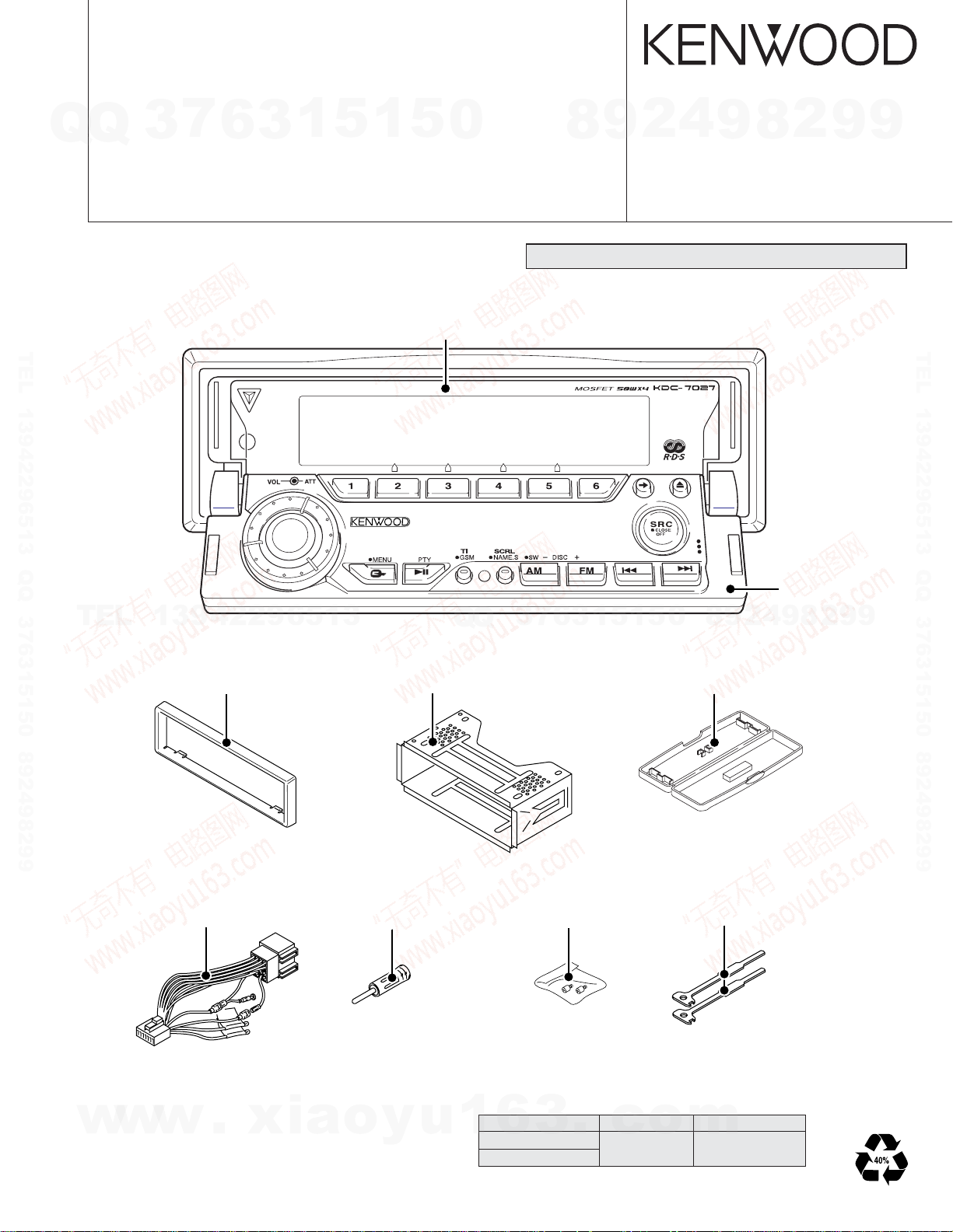
Panel assy
TEL 13942296513 QQ 376315150 892498299
TEL
13942296513
(A64-3234-01)
Q
Q
3
7
4
2
9
8
© 2004-02 PRINTED IN JAPAN
B53-0129-00 (N) 1839
CD mechanism extension cord (24PIN) : W05-0935-00
0
5
1
5
1
3
6
9
8
9
2
2
8
Panel assy
(A64-3253-02)
9
4
8
9
2
9
9
9
TEL 13942296513 QQ 376315150 892498299
w
w
DC cord
(E30-4942-05)
w
Escutcheon
(B07-3078-01)
.
xia
Antenna adaptor
(T90-0552-05)
o
y
Mounting hardware assy
(J21-9823-03)
Screw set
(N99-1734-05)
TDF PANEL INFORMATION
u
MODEL PARTS NO. PANEL NAME
1
6
KDC-7027
KDC-7027Y
3
Plastic cabinet assy
(A02-2731-13)
.
c
o
m
Y33-1790-61 TDF-M7000
Lever
(D10-4674-04) x 2
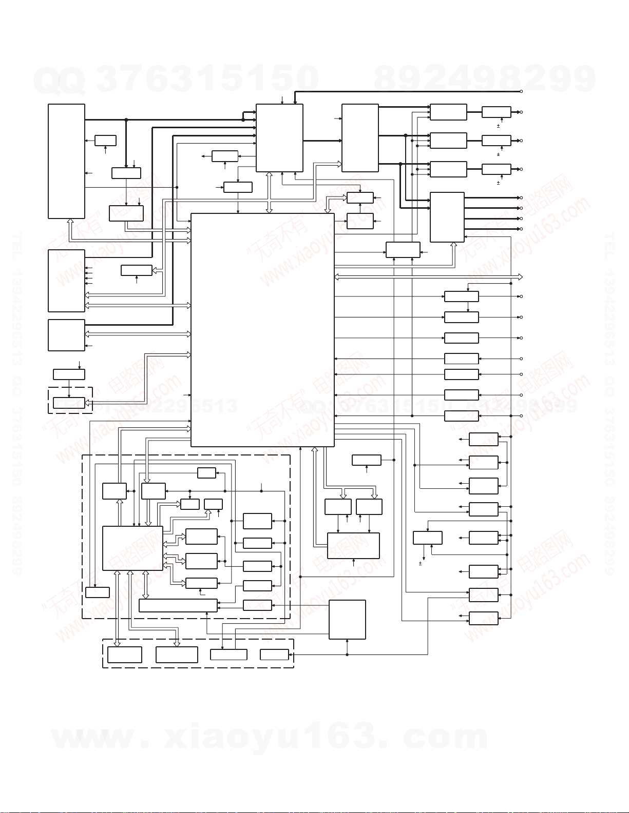
KDC-7027/7027Y
BLOCK DIAGRAM
Q
(X34- )
TUNER
AUDIO OUT
Q
S-METER
3
Q303,304
AM+B
8V 8V
8V
IC14
RDS
DECODER
6
BUFFER
SW5V
7
TEL 13942296513 QQ 376315150 892498299
CD
BU5V
EEPROM
8V
SERVO
CH
BU5V
Q501
EEP5V
IC1
EEPROM
TEL
TDF UNIT
(X16-208)
DISPLAY
UNIT
(X16-254)
SWITCH UNIT
(X16-256)
CD4.7V
BACK UP
REMO
SW5V
13942296513
IC7
LEVEL
SHIFT
IC11
IC9
ROT ARY
ENCODER
u-COM
LEVEL
SHIFT
IC8
KEY MATRIX
3
BU5V
FL
KEY
BPF
IC1
IC2
IC4
FLASH
ROM
IC10
1
SW5V
2.5V
MASK
ROM
BPF
5
AGC
8V
BUFFER
LEDLED
ILL+
AGC
RESET SW
1
5
8V
IC2
FM
AM
CD
E-VOL
CH
&
MPX
QUAL
SYSTEM
MICROPROCESSOR
PANEL5
Q6,10
PANEL
SW5V
IC6
3.3V
Q5
SW3.3V
Q4
FL3.3V
Q2,3
FL+B
KEY ILL
0
Q
Q
8V
IC15
MOTOR
FL+B
FAC
IC5
SYSTEM
E'S+
IC20
FOCUS
SW
3
IC8
SERVO
PANEL
MECHA
SW5V
DC/DC
WOW
7
IC6
6
RESET
BU5V
IC16
MOTOR
DRDR
8
8V
8V
IC9
3
9
MUTE
DRIVER
5
1
2
Q207,208
PRE MUTE
Q203,204
PRE MUTE
Q205,206
PRE MUTE
IC4
POWER
IC
BU5V
0
5
1
BU5V
SW5V
PANEL5V
SW14V
DC/DC A8V
9V
SERVO
CD4.7V
4
9
IC13
OP AMP
IC12
OP AMP
IC11
OP AMP
IC18
P-CON P CON
Q23,24
ANT-CON ANT CON
Q25
EXT AMP
Q26
DIMMER DIMMER
TEL MUTE
Q29
ACC DET
Q27
B.U DET
9
8
Q1,2
BU5V
Q3,601
SW 5V
Q502,503
PANEL
5V
Q4,5
SW 14V
Q6-8
A8V
Q9,602
SERVO
Q11-14
FL+B
IC19
SW REG
2
8
9V
9V
9V
4
2
AUX IN
PRE OUT
(SUB WOOFER)
PRE OUT
(REAR)
PRE OUT
(FRONT)
SP OUT (FL)
SP OUT (FR)
SP OUT (RL)
SP OUT (RR)
WIRED REMO/
OPEL DISP I/F
EXT.AMP.CON
TEL MUTE
ACC
8
9
BACK UP
9
2
9
9
TEL 13942296513 QQ 376315150 892498299
9
2
w
w
w
.
xia
o
y
u
1
6
3
.
c
o
m
BLOCK DIAGRAM
KDC-7027/7 027Y
7
Q
Q
3
TEL 13942296513 QQ 376315150 892498299
6
CD PLAYER UNIT
(X32-5550-00,01)
PICK-UP
A
EF
C
B
TR COIL
FO COIL
SPINDLE
MOTOR
LOADING
& SLED
MOTOR
M1
M2
3
M
M
2
2
1
D. GND
Q1
APC
2
2
MOTOR
DRIVER
LOADING
SLED
5
7
IC3
VREF
H
L
1
IC1
RF AMP
S. GND
D. GND
VREF
5
14
7
0
IC2
1 CHIP IC
SERVO
PROCESSOR
u-COM
VREF
DRV MUTEMUTE
X1
CLOCK
16.93MHz
PON
LOE/LIM
A+5V
REF
A. GND
D. GND
SW +5V
D. GND
8
D2
5V REG
9
IC4
Q4
5V SW
Q5
(0-01)
ONLY
SW
LPF
2
Q3
8V SW
Q2
SW
4
S3
S4
S2
S1
4
2
9
MOTHER
BOARD
DOUT
CLK
DATA
MSTOP
MRST
MUTE L
MUTE R
L-ch
R-ch
A8V
A. GND
BU5V
D. GND
LOE/LIM SW
8EJE SW
12EJE SW
LOS SW
S7.5V
S. GND
MOTOR
LO/EJ
DXM-6120V
8
24
21
20
12
13
14
15
18
16
19
17
9
8
10
11
23
22
2
1
3
4
2
9
9
TEL 13942296513 QQ 376315150 892498299
TEL
13942296513
Q
Q
3
7
6
3
1
5
1
5
0
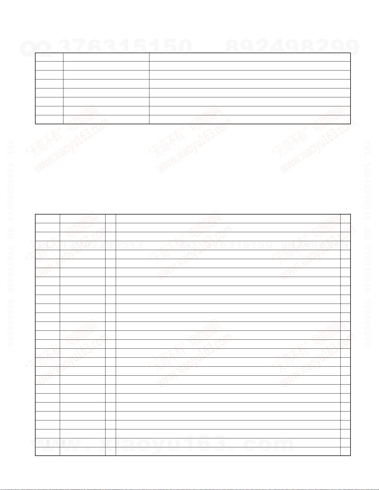
COMPONENTS DESCRIPTION
● SUB CIRCUIT UNIT (X16-2080-10)
Ref No. Application / Functions Operation / Condition / Compatibility
IC1 E2PROM E2PROM for security
● DISPLAY UNIT (X16-2540-10)
Ref No. Application / Functions Operation / Condition / Compatibility
IC1 Driver LCD driver (Include KEY input function)
IC2 Driver LCD driver
IC3 Remote control IC For Remote control sensor
Q1 SW Key scan start SW “ON” when Q1 base level goes L
Q2 Red LED SW Red LED is turned on when Q2 base level goes H
Q5 VLCD AVR Reference voltage
Q6 SW Power supply control SW “ON” when base level goes L
Q11 Dimmer control LCD back light control “OFF” when Q11 base level goes L
w
w
D26 VLCD AVR Reference voltage
w
.
xia
o
y
u
1
6
3
.
c
o
9
8
m
2
4
9
8
2
9
9
3
KDC-7027/7027Y
COMPONENTS DESCRIPTION
7
Q
Q
● SWITCH UNIT (X16-2560-11)
Ref No. Application / Functions Operation / Condition / Compatibility
Q1 DSI LED SW DSI LED blinks when Q1 base level goes H/L
Q2 KEY Illumination SW (Green) KEY Illumination SW “ON” when the Q2 base level goes H
Q3 KEY Illumination SW (Red) KEY Illumination SW “ON” when the Q3 base level goes H
Q4 KEY Illumination SW (Blue) KEY Illumination SW “ON” when the Q4 base level goes H
● CD PLAYER UNIT (X32-5550-00)
Ref No. Application / Functions Operation / Condition / Compatibility
TEL 13942296513 QQ 376315150 892498299
IC1 RF amplifier adapted for CD-RW
IC2 CD signal processor built-in MI-COM
IC4 4CH BTL driver Focus, Tracking coil, Feed and Spindle motor driver IC
IC6 LPF Audio active LPF
Q1 APC LD power control
Q2 Q3 SW When P ON signal gose “H”, Q2 is ON
Q3 A.8V SW When P ON signal gose “H” (Q2 is ON), Q3 is ON
TEL
Q4 D.5V SW When P ON signal gose “L” (Q5 is ON), Q4 is ON
Q5 Q4 SW (P-ON) When P ON signal gose “H”, Q5 is ON
3
13942296513
6
3
1
5
1
5
0
Generation of RF signal based on the signals from the APC circuit and pickup, and
generation of servo error (focusing error and tracking error) signals. Detection of dropout,
anti-shock, track crossing and off-track conditions, included gain control function during
CD-RW.
Focusing, tracking, sled and spindle servo processing. Automatic adjustment (focusing,
tracking, gain, offset and balance) operations. Digital signal processing (DSP, PLL, subcodes, CIRC error correction, audio data Interpol ration) operations, and Microcomputer
function.
7
3
Q
Q
6
8
3
9
1
5
1
2
5
4
0
9
8
9
8
2
4
2
9
8
9
2
9
9
TEL 13942296513 QQ 376315150 892498299
9
● ELECTRIC UNIT (X34-3042-72)
Ref No. Application / Functions Operation / Condition / Compatibility
IC1 System control IC System control microprocessor
IC2 E-VOL & tuner IC E-VOL. FM/AM tuner & stereo decoder
IC3 Power supply IC For A8V AVR
IC4 Audio power IC Audio power amplifier
IC7 Reset IC When BU5V line voltage is less than 3.5V, this IC output line is “L”
IC8 Muting logic IC Control for MUTE, P-ANT & RESET muting
IC12 RDS decoder Decode for RDS signal
IC13,14 Motor driver Control for Panel mechanism motor
Q1,2 BU 5V AVR While BU is applied when BU5V regulator output is +5V
Q3 SW5V AVR When Q3base level goes L, SW5V regulator output is +5V
Q4,5 SW14V AVR When Q5 base level goes H, SW14V regulator output is +14V
Q6~8 Audio 8V AVR When Q6 base level goes H, A8V regulator output is +8.4V
Q9,34 Servo +B AVR When Q34 base level goes H, S+B regulator output is +7.4V
Q11~14 Illumination +B AVR When Q11 base level goes H, AVR output is +10.5V
Q25,26 P-CON SW When Q26 base level goes H, P-CPN SW output is +14V
Q27,28 P-CON protection Protect Q27 by turning on when P-CON output is grounded
Q29 Buffer EX amp control buffer
w
w
Q30 Small lamp det. SW When Q30 base level goes H, Q30 turned ON
w
.
xia
o
y
u
1
6
3
.
c
o
m
4
KDC-7027/7 027Y
COMPONENTS DESCRIPTION
7
Q
Q
Q32 BU detector When Q32 base level goes H, Q32 turned ON
Q33 ACC detector When Q33 base level goes H, Q33 turned ON
Q51,52 Muting driver When base level goes L, muting driver is turned ON
Q55,56,59,60
Q63 E2P 5V SW When Q63 base level goes L, E2P 5V is out for E2P ROM
Q102,103 AM +B SW When Q102 base level goes H, AM +B is out to tuner unit
Q104 Buffer Composite signal buffer for RDS
TEL 13942296513 QQ 376315150 892498299
● SYSTEM MICROPROCESSOR : UPD703030GC043 (X34-304 : IC1)
1 PLL DATA I/O Data input/output terminal for Tuner front-end
2 AM+B I/O AM+B (AM operation : H)
3 (FM+B) O FM+B (FM operation : H, Last FM : H with RDS,RBDS model)
TEL
4PAN E2P DATA I/O Variable illumination D/A converter, E2PROM DATA terminal
5PAN E2P CLK I/O Variable illumination D/A converter, E2PROM CLK terminal
6 EVDD - VDD 5V
7 EVSS - GND
8 AFS O Time constant switching for noise detection (FM seek, AF search, AUTO 0 : L, Receiving : H)
9 BEEP O BEEP audio output terminal
10 REMO I Remote control input terminal
11 P MUTE O Audio power IC muting control terminal (POWER OFF, ALL OFF, TEL MUTE : L)
12 SVR O Audio power IC SVR discharge circuit control terminal
13 IC2 SDA I/O CD mechanism, IC2, IC5, ROM correction DATA line
14 IC2 CLK I/O CD mechanism, IC2, IC5, ROM correction CLOCK line
15 P STBY O Audio power IC Stand-by terminal (POWER IC ON, ALL OFF : H, POWER IC OFF : L)
16 P CON I/O Power control terminal (POWER ON : H, POWER OFF, ALL OFF : Hi-Z)
17 DIMMER CONT O Dimmer control terminal (W-LED only : Pulse control F=1KHz, Normal : H)
18 TEST - NC (GND)
19 TYPE2 I Destination select terminal
20 MUTE O MUTE output terminal (ON : OPEN, OFF : L)
21 PRE MUTER O PREOUT (Rch) muting control terminal
22 PRE MUTEL O PREOUT (Lch) muting control terminal
23 BU DET I
24 ACC DET I ACC detection terminal (With ACC : L, Without ACC : H)
25 SW5V I/O SW5V control terminal (OFF : H, ON : L)
w
26 EXT AMP CONT O External amplifier control terminal
3
Ref No. Application / Functions Operation / Condition / Compatibility
Pre-out muting SW When base level goes H, Pre-output is muted
Pin No. Pin Name I/O Description / Processing Operation
13942296513
w
w
6
MICROCOMPUTER’S TERMINAL DESCRIPTION
.
xia
1
5
1
y
5
u
0
Q
Q
1
3
6
7
3
3
Momentary power dropped detection terminal (No Backup, Momentary power dropped : H, Backup : L)
o
6
8
3
.
9
1
1
5
c
2
5
o
4
0
m
9
8
9
8
2
4
2
9
8
9
2
9
9
TEL 13942296513 QQ 376315150 892498299
Fig.
9
5
KDC-7027/7 027Y
MICROCOMPUTER’S TERMINAL DESCRIPTION
7
Q
Q
Pin No. Pin Name I/O Description / Processing Operation
27 DIMMER I Small lamp detection terminal (ON : L, OFF : H)
28 ANT CONT I/O Antenna control/ Destination select terminal (TUNER ON : H)
29 P ON I/O SW14V, SW5V control terminal (POWER ON : H, POWER OFF : Hi-Z)
30 ILL ON I/O FL, illumination control terminal (ON : H, OFF : Hi-Z)
31 RESET I Reset input terminal
32,33 XT1/XT2 - Sub clock (32.768KHz)
34 REGC - Connect to 1µF capacitor
35,36 X2/X1 - Main clock (20MHz)
TEL 13942296513 QQ 376315150 892498299
37 VSS - GND
38 VDD - AVR 5V
39 CLKOUT - NC
40 LX REQ M O Communication request to external slave unit (Request : L)
41 LX MUTE I Mute request from external slave unit (MUTE : H)
42 LX CON O External slave unit (ON : H, OFF : L)
43 LX RST O Reset output to external slave unit (Normal : L, After system reset : H 400ms or more and then L)
44 CD MECHA+B O CD4.7V output terminal (CD : H, Except CD source : L)
45,46 TYPE0/TYPE1 I Destination select terminal
47,48
49 NC - NC
50 E2P5V I/O E2PROM, D/A converter power supply control terminal (ON : L, OFF : Hi-Z)
51 DSI I/O DSI control (ON : L, OFF : Hi-Z)
TEL
52 L CE O CE output to LCD driver IC
53 L INH O INN output to LCD driver IC (Normal : H reset, Momentary power dropped : L)
54 VOL A I Volume input terminal
55 DVDD - AVR 5V
56 DVSS - GND
57 VOL B I Volume input terminal
58 M RST O Reset output to CD mechanism (Normal : H, Reset : L)
59 M STOP O Stop request to CD mechanism (STOP : L, CD : H)
60 CD SW3 I CD DOWN SW detection terminal (CD disc chucking : H)
61 LO/EJ I/O CD mechanism loading/eject selector (STOP, Brake : Hi-Z, LOADING : L, EJECT : H)
62 MOSW O CD mechanism motor driver SW (LOADING, EJECT, Brake : H)
63 FPM MOTOR B O FPM mechanism (Slider) control terminal 1
64 FPM MOTOR F O FPM mechanism (Slider) control terminal 1
65 FPM MOTOR O O FPM mechanism (Angle) control terminal 1
66 FPM MOTOR C O FPM mechanism (Angle) control terminal 1
67 O DATA I/O External display DATA terminal 1
68 O CLK I/O External display CLK terminal
69 O CE I/O External display chip enable terminal
70 M MUTER I Mute request from CD mechanism (Rch ON : L)
71 AVDD - AVR 5V
72 AVSS - GND
73 AVREF I Connect to P-ON (29PIN)
w
74 M MUTEL I Mute request from CD mechanism (Lch ON : L)
3
IC2 TYPE0/TYPE1
13942296513
w
w
6
.
xia
1
5
1
y
5
u
3
I IC2 destination select terminal
o
0
Q
Q
1
3
6
7
3
6
8
3
.
9
1
1
5
c
2
5
o
4
0
m
9
8
9
8
2
4
2
9
8
9
2
Fig.
9
9
TEL 13942296513 QQ 376315150 892498299
9
6
KDC-7027/7027Y
MICROCOMPUTER’S TERMINAL DESCRIPTION
7
Q
Q
75 PAN DET I PANEL, E2PROM detection terminal (With panel : L, Without : H)
76 PHONE I PHONE detection terminal (TEL MUTE : 1V or less, NAVI MUTE : 2.5V or more)
77 FPM SW4 I
78 FPM SW1 I FPM mechanism position detect terminal 1
79 FPM SW2 I FPM mechanism position detect terminal 1
80 FPM SW3 I FPM mechanism position detect terminal 1
81 FPM PHOUT I FPM mechanism position detect terminal (2.2V or more : H) 1
TEL 13942296513 QQ 376315150 892498299
82 S METER I S meter detection terminal
83 NOISE I FM noise detection terminal
84 IFC OUT I Front end IFC OUT input terminal (Receiving station : 2.5V or more)
85 POWER DET I Audio power IC DC offset detection
86 CD SW4 I 8cmDISC detection terminal (8cmDISC : L)
87 R CLK I RDS decoder clock input terminal
88 LX REQ S I Receive request from external slave unit (Request : L)
89 SC REQ I Communication request from panel microprocessor
90 CD SW1 I LOADING SW detection terminal (LOADING start, POWER OFF : L)
91 CD SW2 I 12cmDISC detection terminal (12cmDISC, POWER OFF : L)
92 R QUAL I RDS decoder QUAL input terminal
93 R DATA I RDS decoder DATA input terminal
94 LX DATA S I Data input from external slave unit
TEL
95 LX DATA M O Data output to external slave unit
96 LX CLK I/O Clock input/ output with external slave unit
97 L DATAL I Data input from LCD driver
98 L DATAS O Data output to LCD driver
99 L CLK O CLK output to LCD driver
100 PLL CLK I/O Clock input/ output to Tuner front-end
3
Pin No. Pin Name I/O Description / Processing Operation
13942296513
6
1
5
1
3
FPM mechanism position detect/ CD Mechanism detection terminal
(3.75V or more : No mechanism, 1.25V or more : H, Less than 1.25V : L)
5
0
Q
Q
3
7
6
8
3
9
1
5
1
2
5
4
0
9
8
9
8
2
4
2
9
8
9
2
9
9
Fig.
1
9
TEL 13942296513 QQ 376315150 892498299
Fig.1 FPM motor control
SLIDE FPM mechanism
FPM MOTOR B FPM MOTOR F operation
LLStandby
HLBackward operation
LHForward operation
HHBrake
● CD SIGNAL PROCESSOR & CD MECHANISM CONTROL : MN662773KH2 (X32-555 : IC2)
Pin No. Pin Name I/O Description / Processing Operation
1 BDO I Dropout signal input (H : Dropout detected)
2 OFT I Off-track signal input (H : Off-track detected)
3 /RFDET I RF detection input (H : RF signal detected)
4 VDET I Vibration detection input (H : Vibration detected)
w
w
5 LDON O Laser diode ON signal output (H : Laser diode ON)
w
.
xia
o
y
u
FPM MOTOR O FPM MOTOR C operation
1
6
ANGLE FPM mechanism
LLStandby
HLAngle open direction
LHAngle close direction
HHBrake
3
.
c
o
m
7
KDC-7027/7 027Y
MICROCOMPUTER’S TERMINAL DESCRIPTION
7
Q
Q
Pin No. Pin Name I/O Description / Processing Operation
6,7 NC - Not used (N.C.)
8AVSS3 - GND
9AVDD3 - VDD (BU5V)
10 FBAL O Focusing balance adjustment output
11 TBAL O Tracking balance adjustment output
12 FE I Focusing error signal input
13,14 NC - Not used (N.C.)
15 TE I Tracking error signal input
TEL 13942296513 QQ 376315150 892498299
16-18 NC - Not used (N.C.)
19 REFNV I RF envelope signal input
20 VREF I VREF input terminal
21 ARF I RF signal input (for DSL)
22 DRF I DSL bias terminal
23 DSLF I/O DSL loop filter terminal
24 IREF I Reference current input terminal
25 PLLF I/O PLL loop filter terminal
26 PLLF2 I/O PLL loop filter characteristic switching terminal
27 VCOF I/O VCO loop filter terminal
28 VCOF2 I/O VCO loop filter terminal Digital servo 33.8688MHz generation
29 TRV O Traverse forced feed output
30 TVD O Traverse drive output
TEL
31 PC O Spindle motor ON/OFF output (Lo : ON)
32 ECM O Spindle motor drive output (forced mode output)
33 ECS O Spindle motor drive output
34 KICK O Kick pulse output
35 TRD O Tracking drive output
36 FOD O Focusing drive output
37 TOFS O Tracking off-set adjustment output
38 AVDD2 - VDD (BU5V)
39 AVSS2 - GND
40 DVSS2 O GND
41 EFM or CK384 O EFM signal output
42 PCK or DSLB O PLL sampling clock output
43 /CLDCK O Sub-code frame clock signal output
44 FCLK O Crystal frame clock signal output
45 IPFLAG O Interpolation flag signal output (H : Interpolated)
46 FLAG O Flag signal output
47 TRCRS I Track crossing signal input
48 STOUT O Serial data output for monitor signal
49 STLD O Load output for monitor signal
50 SMCK O Bit clock signal output for monitor signal
51 CSEL I Crystal oscillation frequency selection terminal (Hi : 33.8688MHz, Lo : 16.9344MHz)
52 TEST1 I Test terminal 1 Not used (Connected to GND lines)
w
53 TEST2 I Test terminal 2 Not used (Connected to GND lines)
3
13942296513
w
w
6
.
xia
3
1
5
o
1
y
5
u
0
Q
Q
1
3
6
7
3
6
8
3
.
9
1
1
5
c
2
5
o
4
0
m
9
8
9
8
2
4
2
9
8
9
2
9
9
TEL 13942296513 QQ 376315150 892498299
9
8
KDC-7027/7027Y
MICROCOMPUTER’S TERMINAL DESCRIPTION
7
Q
Q
54 IOSEL I Audio DAC data input mode selection terminal (H : External data, L : Internal data)
55 NRST I Reset input (L : Reset)
56 BCLK O Bit clock output for SRDATA
57 LRCK O L/R identification signal output
58 SDDATA O Serial data output
59 SUBC O Sub-code serial output
60 SBCK I Clock input for Sub-code serial output
61 DQSY O CD-TEXT read permission signal output
TEL 13942296513 QQ 376315150 892498299
62 DEMPH O De-emphasis detection signal output (H : ON)
63 TX O Digital audio interface signal output
64 PSEL I SRDATA input/Test terminal
65 MSEL I LRCK input/SMCK output frequency switching
66 SSEL I BCLK input
67 DVDD1 - VDD (BU5V)
68 X1 I Crystal oscillation circuit connection terminal
69 X2 O Crystal oscillation circuit connection terminal
70 DVSS2 - GND
71 XSUB1 I Microprocessor clock input terminal
72 XSUB2 O Microprocessor clock output terminal
73 DVDD2 - VDD (BU5V)
74,75 NC O Not used (N.C.)
TEL
76 73/74SEL I 73/74 selection terminal (H : CD-TEXT OFF, L : CD-TEXT ON)
77 DRV MUTE O Driver muting control terminal (L : Spindle motor, Focusing actuator and tracking actuator outputs OFF)
78,79 NC O Not used (N.C.)
80 TEST I Test mode switching terminal
81 ASEL I Audio output polarity detection terminal (H : Non inverted, L : Inverted)
82 PON O Audio/digital power supply control terminal (H : Power ON)
83 SEARCH O Servo IC gain switching control terminal (H : Search, L : Normal operation)
84 EQCNT O RF amplifier doable-speed switching control terminal
85 SW3 I Limit switch detection terminal (H-L : Pickup most inner position)
86 /AMUTE L O L ch. analogue muting control terminal (L : Muting requested)
87 /AMUTE R O R ch. analogue muting control terminal (L : Muting requested)
88 CD-RW O CD-RW control terminal (H : CD-RW, L : Normal operation)
89 /RST I System reset input terminal (L : System reset)
90 MECHASEL I 6000/6010 selection terminal (L : 6000 series, H : 6010 series)
91 /MSTOP I Standby detection terminal (H : Operation mode, L : Stop mode)
92 LDCNT O LD control terminal (H : LD ON, L : LD OFF)
93 DATA I/O I2C bus data line (communication line with System microprocessor)
94 /CLK I/O I2C bus clock line (communication line with System microprocessor)
95 HOT I Temperature protection detection terminal
96 AVREF - A/D converter reference voltage connection terminal (Connected to BU 5V lines)
97 OUT R O R ch. Audio output
98 AVDD1 - A/D converter positive power supply connection terminal (Connected to analogue 5V lines)
w
99 OUT L O L ch. Audio output
100 AVSS1 - GND
3
Pin No. Pin Name I/O Description / Processing Operation
13942296513
w
w
6
.
xia
3
1
5
o
1
y
5
u
0
Q
Q
1
3
6
7
3
6
8
3
.
9
1
1
5
c
2
5
o
4
0
m
9
8
9
8
2
4
2
9
8
9
2
9
9
TEL 13942296513 QQ 376315150 892498299
9
9
KDC-7027/7 027Y
TEST MODE
7
Q
Q
● How to enter the test mode
While pressing and holding the Preset 1 and Preset 3 keys,
reset the unit.
● How to exit from the test mode
While holding the Preset 6 key, reset the unit.
Note : Turning ACC off, po wer off, momentary power down
or panel detaching does not terminate the test mode.
TEL 13942296513 QQ 376315150 892498299
● Initial status in the test mode
• Sources : ALL OFF
• Display : All segments are lit.
• Volume : -10dB (displayed as “30”)
• Loudness : OFF
• CRSC : OFF regardless of the presence of switching function.
• SYSTEM Q : Flat
• WOW : All OFF
• BEEP : When pressing any keys, the buzzer generates a
beep at any time.
• AUX : ON
• MENU SYSTEM Q : OFF
• Variable model : Default is white
TEL
• Multifunction : Source dependency (Preset, SCAN, etc.)
● Special display in Tuner mode
When any of the following messages is displayed in Tuner
mode, the F/E may be abnormal.
• “TNE2P NG” : The EEPROM is set to the default (unstable
values) because the F/E was shipped without passing
through the adjustment process, etc.
• “TNCON NG” : Comm unication with the F/E is not possible.
● Forced switching of K3I
Each press of the Preset 6 key in Tuner mode should switch
K3I from AUTO→Forced Wide→Forced Middle→Forced
Narrow→AUTO.
The initial status is AUTO and the display shows these
modes as follows.
• AUTO : FMA
• Forced Wide : FMW
• Forced Middle : FMM
• Forced Narrow : FMN
w
3
13942296513
w
w
6
.
xia
3
1
5
o
1
y
5
u
0
● Test mode specifications of the CD receiver
•Forced ejection is inhibited in the reset start operation. When
the unit is reset while a CD is loaded in it, resetting does
not recognize the CD.
• Each press of the Track Up key jumps to the f ollowing track
numbers :
No. 9→No. 15→No. 10→No. 11→No. 12→No. 13→No. 22
→No. 14→No. 9 (The cycle restarts from here.)
• Each press of the Track Down key jumps to the previous
track number to the track being played.
•When the number of total trucks of the MP3 disc or the
WMA disc is less than 9, 1st truck is played.
• When the disc media is CD, A short press of the Preset 1
key jumps to the track number 28.
• When the model is equipped the CD mechanism assembly
adapted for MP3 or MP3/WMA disc, the mechanism name
and version number are displayed during the FL model is
lower stand and Display mode of LCD model is DNPS.
● Audio-related specifications
• Pressing the ✽ ke y on the remote initiates the audio adjustment mode.
• BL/F key on the Fader initials.
7
3
Q
Q
• Continuous holding of a remote control key is inhibited, and
workings are short press of any keys.
• Bass, Middle and Treble are adjusted in 3 steps of -8 / 0 /+8
with the Track Up/Down keys (Default value at 0).
• Balance is adjusted in 3 steps of L15 / 0 / R15 with the
Track Up/Down keys (Default value at 0).
•Fader is adjusted in 3 steps of R15 / 0 / F15 with the Track
Up/Down keys (Default value at 0).
• HPF is adjusted in 2 steps of OFF / 170Hz (or 200Hz) with
the Track Up/Down keys (Default value at OFF).
• LPF is adjusted in 2 steps of OFF / 120Hz with the Track
Up/Down keys (Default value at OFF).
• Bass f, Bass Q, Bass EXT, Middle f, Middle Q and Treble f
are not dealt with by the audio adjust.
• The WOW key passes during the audio adjustment as following steps (WOW model only).
Ordered TruBass FOCUS SRS Display
1 OFF OFF OFF SRS WOW OFF
2ONOFF OFF SRS T ruBass ON
3 OFF LOW OFF FOCUS LOW
4 OFF HIGH OFF FOCUS HIGH
5 OFF OFF ON SRS ON
1
6
3
6ONHIGH ON SRS WOW HIGH
6
8
3
.
9
1
1
5
c
2
5
o
4
0
m
9
8
9
8
2
4
2
9
8
9
2
9
9
TEL 13942296513 QQ 376315150 892498299
9
10
TEST MODE
KDC-7027/7027Y
7
Q
Q
● Menu-related specifications
• A short press of the Q key initiates the menu mode.
• Pressing the DNPP key on the remote initiates the Menu
• Continuous holding of a remote control key is inhibited, and
• Contrast is adjusted in 3 steps of 0 / 5 / 10 with the Track
TEL 13942296513 QQ 376315150 892498299
● Backup current measurement
● Special display when the display is all on
[PRESET 1]
TEL
[PRESET 2]
[PRESET 3]
[PRESET 4]
[PRESET 5]
[PRESET 6]
FM key Display ROM collection version.
w
3
mode.
workings are short press of any keys.
Up/Down keys (Default value at 5).
When the unit is reset while ACC is OFF (i.e. by turning
Backup ON), the MUTE terminal goes OFF in 2 seconds in
place of 15 second. (The CD mechanism is not activated at
this time.)
Pressing the Preset keys while the power is ALL OFF displays the following information.
13942296513
w
w
6
Version display (8 digits, Month/Day/Hour/Minute)
(Display) SYS xxxxxxxx :
PAN xxxxxxxx : FL model only
MEM
Serial number display (8 digits)
(Display) SNo xxxxxxxx
Short press : View power ON time. (The All OFF
period is not counted.)
2 seconds long press/hold : Clear power ON time
at the power ON time displaying.
(Display) PonTim xxxxx Max. 60000 (hours)
Short press : Display CD operation time.
2 seconds long press/hold : Clear CD operation
time at the CD operation time displaying.
(Display) CDTim xxxxx Max. 60000 (hours)
Short press : Display CD ejection count.
2 seconds long press/hold : Clear CD ejection
count at the CD ejection count displaying.
(Display) EjeCnt xxxxx Max. 60000 (times)
Short press : Display Panel open/close count.
2 seconds long press/hold : Clear Panel open/close
count at the Panel open/close count.
(Display) PnCnt xxxxxx Max. 600000 (times)
.
(Display) ROM R xxx Invalid : “R – – –”
xia
1
3
xxxxxxxx :
5
1
5
4 contrasts FL model only
o
y
u
0
Q
Q
1
AM key Display panel E2PROM condition.
● Panel mechanism
• Auto-panel close inhibition when set-in the CD.
• The panel operation inhibition at power ON/OFF and ACC
ON/OFF.
• The panel position changing Eject→Last with a short press
of the PLAY/PAUSE keys.
● Other specifications
• No displays such as “CODE OFF/ON” during Power-ON.
• The LINE MUTE inhibition time is one second from 10 seconds when start-up the test mode.
• Do not write the security code with the security jig on the
test mode.
• Do not write the serial with the serial writing jig on the test
mode.
• OEM display output is not stop if OEM display not connec-
7
3
tion on the test mode.
● Demonstration mode
1. How to enter to the Demonstration mode
1. Hold down the [Q] key and [TI (AME)] k ey button when the
power is on and press the Reset button.
2. This will enter to the Demonstration mode.
2. How to chancel the Demonstration mode
1. Hold-down the Preset [5] key button when the power is on
and press the Reset button.
2. This will cancel the Demonstration mode.
6
3
4
2
9
8
(Display) P–ROM OK (Registered code)
P–ROM NG (Code is write in error)
P–ROM WAIT (Unregistered code)
P-ROM NON
0
5
1
5
1
3
6
.
c
o
9
8
m
2
8
(Panel security nonfunctional)
2
8
9
4
2
9
9
9
9
9
TEL 13942296513 QQ 376315150 892498299
11

KDC-7027/7 027Y
TEST MODE
7
Q
Q
● Security information
1. Forced Power ON mode (All models)
Even when the security (Cord) is approved, resetting the
unit while holding the Q and Preset 4 keys makes it possible to turn the power ON for 30 minutes.
After 30 minutes have elapsed, it is not possib le to return to
the previous condition unless the unit is reset again. (Security code is doing not clear at this mode. Put the power on
fill-in.)
TEL 13942296513 QQ 376315150 892498299
When panel security was set up for the unit when it is can
not power on.
In this case, you can use new ROM for the TDF panel that
the unit can be power on for test mode.
Note : Don’t enter the panel security set up for new ROM
panel. User can not power on the unit.
2. Method of registration of the security code after
EEPROM (F/E) replacement (Code security model)
1. Enter the test mode. (See How to enter the test mode)
2. Press the MENU key to enter the Menu mode.
3. When the message “Security” is displa yed, press and hold
the Track Up/Down key for 1 second to enter the security
registration mode.
TEL
4. Enter the code using the FM/AM/T r ack Up/Track Down keys.
FM key : Number up
AM key : Number down
Track Up key : Cursor right shift
Track Down key : Cursor left shift
5. Hold down the Track Up key for at least 3 seconds and the
message, “RE-ENTER” appears, so once again enter the
code according to Step 4 above.
6. Press and hold the Track Up key for 3 seconds until “APPROVED” is displayed.
7. Exit from the test mode. (See 2. How to exit from the test
mode)
Note 1 : All Clear is not applicable to the security code of
this model.
Note 2 : When the F/E changed, need re-inscription because the panel security is clear.
3
13942296513
6
3
1
5
1
5
0
3. How to inscription the panel security code
1. Enter the test mode.
2. Pressing the AM key on all lighting, check the “P-ROM W AIT”
display.
3. The NEXT key is long press 2 seconds, writing the code.
4. Display is “P-ROM OK”.
5. Exit from the test mode.
Note : E2PROM connection is NG when displa y is “P-R OM
NG”, so detach the panel and rewrite after the display is
“PROM WAIT”. This code can not clear.
7
3
Q
Q
6
8
3
9
1
5
1
2
5
4
0
9
8
9
8
2
4
2
9
8
9
2
9
9
TEL 13942296513 QQ 376315150 892498299
9
12
w
w
w
.
xia
o
y
u
1
6
3
.
c
o
m
 Loading...