


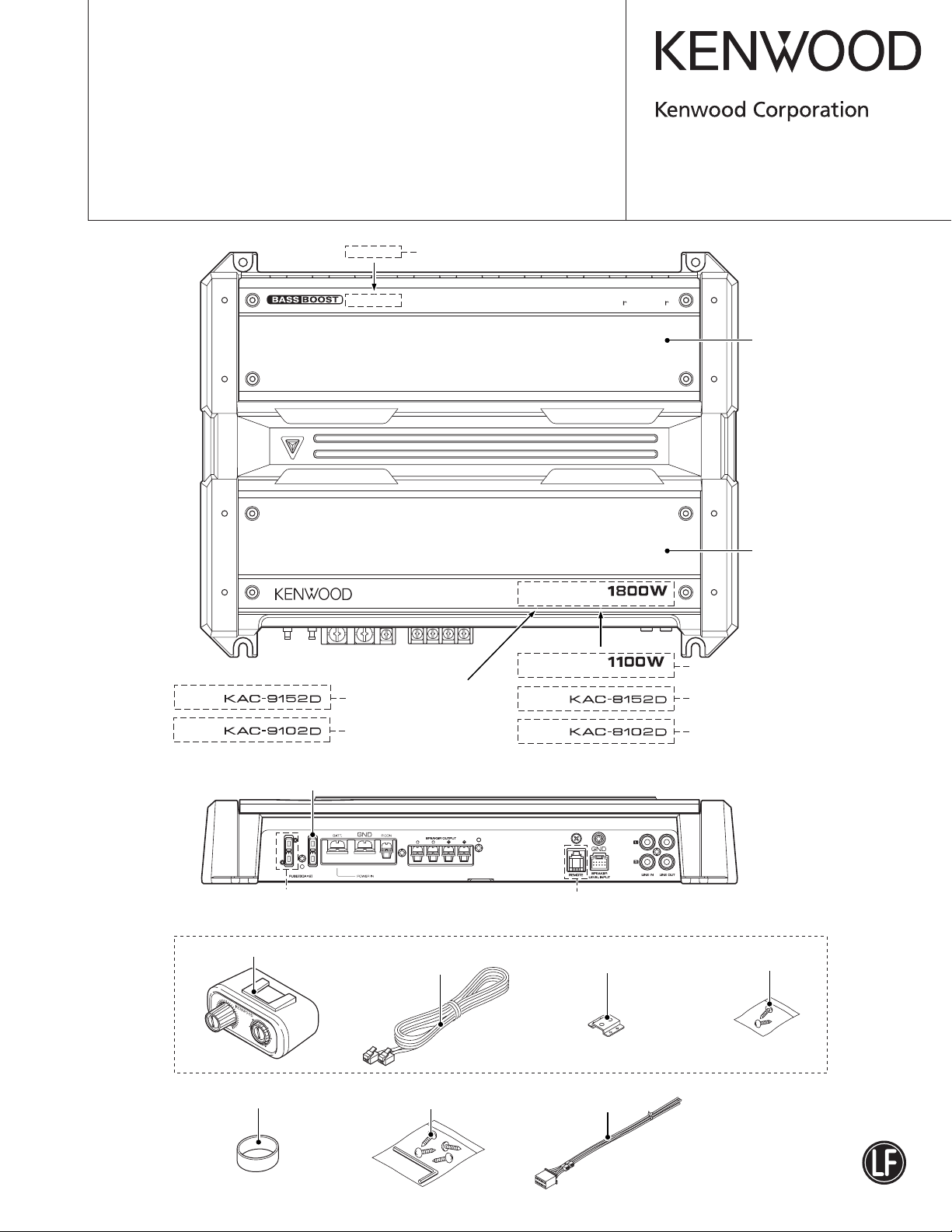
POWER AMPLIFIER
KAC-8102D/8152D
KAC-9102D/9152D
SERVICE MANUAL
© 2005-3 PRINTED IN JAPAN
B53-0252-00 (N) 1708
KAC-9152D
(E type,M type)
CONTROL SYSTEM
REMOTE CONTROL
KAC-8102D/9102D
MAXIMUM POWER
MAXIMUM POWER
Powe
Subwoofer
Amplifie
KAC-9152D
KAC-8152D
Dressing Panel
(A21-4465-02)
: KAC-8152D/9152D
(A21-4466-02)
: KAC-8102D/9102D
Dressing Panel
(A21-4471-02)
: KAC-9152D(K type)
(A21-4472-02)
: KAC-9102D
(A21-4473-02)
: KAC-8152D(K type)
(A21-4474-02)
: KAC-8102D
(A21-4522-12)
: KAC-9152D(E/M type)
(A21-4523-12)
: KAC-8152D(E/M type)
KAC-8152D(E type, M type)
KAC-9152D(K type)
KAC-9102D
Fuse (40A) (F52-0016-05) : KAC-8102D/8152D
Fuse (30A) (F52-0015-05) : KAC-9102D/9152D
Fuse (30A) (F52-0015-05) : KAC-9102D/9152D
Except KAC-8102D/9102D
Remote control
9
1
1
2
1
5
6
5
7
5
1
7
5
0
LEVEL [dB]
8
5
1
8
4
0
FREQUENCY
9
5
1
[Hz]
0
0
Accessories
(W01-1606-05)
Modular cable
(E30-6240-15)
Screw set
(N99-1759-05)
6m
Except KAC-8102D/9102D
Mouting hardware
(J22-0301-14)
Connecting cord assy
(E30-6145-05)
KAC-8152D(K type)
KAC-8102D
Screw set
(N99-1766-05)
19cm
This product uses Lead Free solder.
KAC-8102D/8152D
KAC-9102D/9152D
BLOCK DIAGRAM
LINE IN
LINE OUT
SP IN
X09-5820-10
IC11
50
40
30
20
10
0
-10
X08-4180-10
IC11
ISO
LEVEL DIAGRAM
ISOLATION X08 D CLASS AMP
INPUT
VOL
LEVEL
INV
NOR/REV
Q151
KAC-9152D/9102D
KAC-8152D/8102D
X08
OUT
MUTE
IC11
I.F.S
25Hz
15Hz
IC31
COMPARATOR
TRIANGLE
WAVE
SP
OUT
15V
SENS
Q25,26
+15V
AVR
-15V
AVR
Q28,42
IC12,13
DEAD
TIME
CONT
+15V
AVR
IC13
FREQ
L.P.F
Q401-415,187-190
D CLASS
AMP
THERMAL
PROTECT
HB
Q8-20
BASS
BOOST
KAC-9102D
KAC-8102D
ONLY
OVER
LOAD
DET.
OP
AMP
D.D CON
IC12
LVL
DC
OFFSET
DET.
TR SW
IC51-53
REMOTE
BASS
BOOST
KAC-9152D
KAC-8152D
ONLY
P-CON
DET
R
E
M
KAC-9152D
KAC-8152D
ONLY
SP OUT
P-CON
BATT
GND
IND
LVL
FREQ
2
KAC-8102D/81 52D
KAC-9102D/91 52D
COMPONENTS DESCRIPTION
● PREAMPLIFIER UNIT (X08-4180-1x)
Ref. No. Application / Function Operation / Condition / Compatibility
IC11 (1/2) INFRA SONIC FILTER Cutting super-low area of voice signals
IC11 (2/2) INVERTER Reversing voice signal phase
IC12 (1/2) OP AMP Voltage amplification, buffer
IC12 (2/2) BASS BOOST High-boost (variable levels)
IC14,15 BASS BOOST High-boost (variable levels)
IC13 LOW PASS FILTER Cutting high range of voice signal
● AUDIO UNIT (X09-5820-1x)
Ref. No. Application / Function Operation / Condition / Compatibility
IC1 DC/DC converter IC Create drive signal for switching element
IC2 (1/2) Differential amplifier Detection of temperature, DC, and excess current and hold protection for a certain time
IC2 (2/2) Differential amplifier Containing excess voltage of ±B
IC11 Isolation amplifier Prevention of noise by the electric potential difference of GND
IC12,13 NAND Generation and forming of Dclass section reversal waveform and dead time
IC31 Comparator Digitalize signal by comparing analog signal and triangular wave
IC32 (1/2) Triangular wave generation Reference signal generation for converting analog signals to digital signals
IC32(2/2) Error amplifier Error compensation by feedback from output
IC51~53 OP amp, electronic volume Frequency, variable level BASS BOOST
IC61,62 Comparator
Q1-3 PCON switch Turns on the circuit when ON-signal is impressed on PCON
Q4,5 Mute Mute drive signal generation, Turn LED off
Q8~11 Gate drive DC/DC converter FET gate drive
Q12-20 DC/DC converter DC/DC converter switching
Q25,26,28 AVR ±15V AVR
Q29,30 Tracking when ±15V AVR is OFF Adjusts -15V’ AVR falling to ‘+15V’ AVR falling
Q36 DC/DC converter ON/OFF control Stops DC/DC converter switching when protection is triggered
Q37~38
Q41 4.4V AVR Vref 5V reference AVR
Q42 AVR ±15V AVR
Q43 DC/DC converter ON/OFF control Stops DC/DC converter switching when protection is triggered
Q151 Mute Turning off voice signal
Q187~190 Electric power amplification Dclass large current switching
Q401~415 Pulse amplification and rectifying Generation of signal for driving Dclass final FET
Q416 15V AVR Integration AVR for obtaining Dclass High+B
Q417,418
Q501 Emitter follower
Q601,602 Comparator
Q603 DC/DC converter control
Q604~607
Q608~611 Latch circuit Detection and holding of output excess voltage
DC/DC converter pulse ON/OFF control
Control of ON/OFF of electric Makes the electric power amplification section non-operative for 1.2 seconds when the
power amplification section power is turned on and when protection is triggered
Electric current and voltage conversion
Detection of short-circuiting of SP output and determine excess current for triggering protection
ON/OFF of DC/DC converter drive waveform
Generation of temperature compensation reference voltage for control of electronic volume
Detection of short-circuiting of SP output and determine excess current for triggering protection
Convey IC62 u pin output, result of excess current detection, to IC2 and stop the DC/DC converter
Conversion of current to voltage of the current flowing to final
3
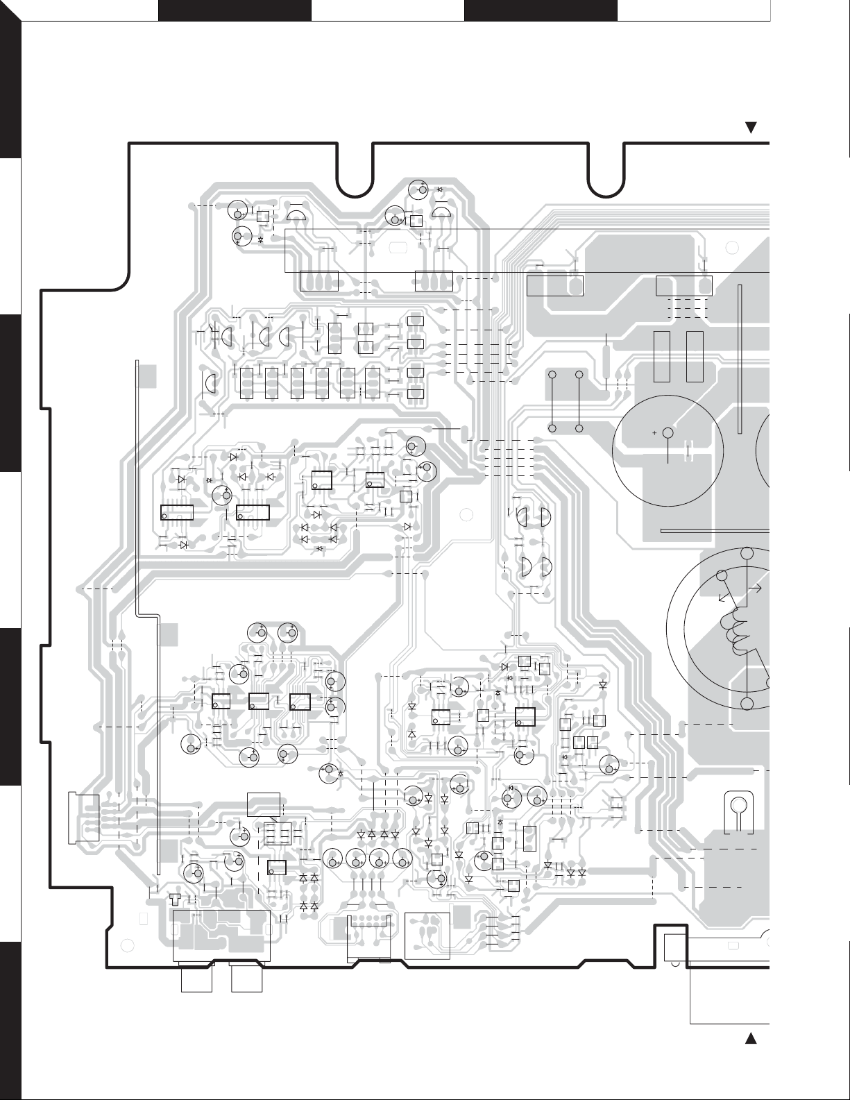
A B C D E
Q
KAC-8102D/8152D
KAC-9102D/9152D
1
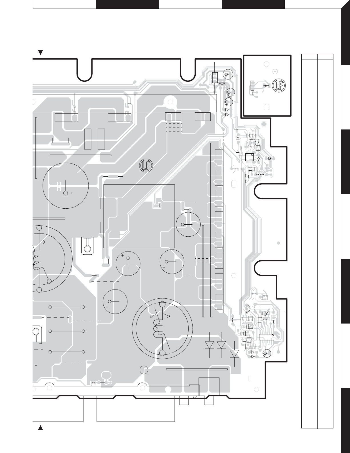
PC BOARD (FOIL SIDE VIEW)
AUDIO UNIT X09-5820-1x A/2 (J76-0072-11)
C31
D23
W65
R154
C152
R156
C108
Q26
R508
R65
Q30
R64
BE
B
R153
BE
D151
W62
W61
W109
D601
C504
D904
W328
J4
BE
R155
C520
W326
EB
EB
E
R152
D602
D502
R151
W59
W60
R52
BE
R66
R53
+15V
Q414
Q410
Q411
Q415
C153
W323
C604
R607
R609
IC61
R605
W324
D906
R527
Q501
BE
R528
R507
13
24
BE
R161
R603
C151
D908
R526
58
41
R604
Q25
R606
D907
R525
W322
W360
R506
W58
W54
C602
C505
D10
C601
W49
W50
Q4
W53
W44
W45
D9
R503
R501
R502
R504
W43
Q603
C603
W57
R509
W52
BE
C5
W46
W56
R608
R12
W356
BE
R602
R11
R13
W321
D603
D607
W55
R601
W320
C4
Q2
R73
R206
R199
BE
Q609
C195
C196
D606
C25
Q611
R10
R68
Q187Q189
W27
W26
W23
W25
C613
R9
W124
W114
SGDDSG
R203
R204
W48
W36
W37
W115
W38
C611
Q607
Q606
E
R627
R625
B
EB
R626
C610
R624
Q605
Q604
W51
EB
EB
R623
W34
W41
Q602
R622
R615
W31
C606
D604
BE
BE
C2
W39
W35
Q608
D605
R638
R640
C614
C612
R8
W33
D11
R74
W29
Q601
BE
W32
R14
R641
R642
C6
Q610
BE BE
W317
W318
W30
D7
W319
C615
R644
R639
R7
D6
R643
C3
BE
BE
R617
R610
R611
D5
R4
R2
R620
R612
D8
Q1
Q5
R616
C607
R621
R619
C609
C608
58
IC62
14
R614
R613
C605
Q3
R3
EB
R5
R6
BE
W40
C501
C503
C502
C519
W22
+B
W122
L4/L14
R200
W19
W20
W21
R629R630
W505
R48
W506
L14
W18
P1
W123
W121
R520
C513
R519
IC53
W75
R67
Q29
R418
R183R184
W81
R61
BE
D25
W351
Q417
R408
W88
D182
814
71
814
71
C527
R120
C111
C113
R116
C110
W79
BE
BE
Q404
W118
C526
IC11
C182
D304
D305
C523
W117
R521
R517
C516
58
41
C109
R115
R57
BE
Q28
Q402
BE
R407
R409
BE
Q406
R305
W110
W339
R304
R306
D303
R516
W77
R518
IC52
C509
W78
R121
R119
W338
C115
D105
R113
R114
Q42
R402
814
71
W337
C116
D106
-15V
R404
R405
IC31
D308
W336
R515
W333
C506
D104
R58
BE
BE
Q407
W332
W72
W73
C107
D103
R410
58
41
R307
D306
W76
R403
BE
D307
C524
C525
J2
R162
C511
R107
Q403
EB
Q413
C510
D501
C105
C156
R159
C302
C301
W74
R111
9
10
W69
W99
BE
BE
W71
D110
R109
W353
C303
R303
R158
C154
IC32
D109
R110
W330
W331
EE
R510
C106
Q409
R112
R108
C35
Q412
Q408
R160
R157
58
41
Q151
R301
W68
D107
1
2
R415
R413
R411
R416
R414
R412
C155
C304
W64
W66
R302
W329
W67
D108
W95
C36
2
3
R426
C406
D402
R424
IC13
R423
C405
W108
W107
W105
W100
W102
R118
R425
R210
W350
C103
D101
D401
C522
R211
W119
R103
C117
4
W106
W104
5
W103
CN1
28
17
6
814
71
W93
R105
W346
R417
W92
R419
C401
C181
R514
W94
R401
D181
C518
C517
W361
R511
W401
R104
C104
C101
Q401
W348
D186
R208
R209
C507
R512
W85
W89
IC51
C114
R420
BE
R182
R181
C508
R523
C515
R522
R529
R106
R101
C32
W354
Q418
+5V
W84
58
41
C102
J1
BE
R406
W355
PWM
D183
W87
R513
R124
R102
C514
W352
BE
Q405
C183
IC12
R117
R122
C112
R123
C521
LINE
OUT
LINE
IN
SPEAKER
LEVEL
INPUT
REMOTE
SPEAKE
7
Refer to the schematic diagram for the values of resistors and capacitors.
4
JIHGF
KAC-8102D/8152D
KAC-9102D/9152D
1
W14
R207
R202
C20
C16
J3
W505
W506
P1
Q190
L4
R201
C26
P2
C40
W15
C198
C199
D4
Q188
R636R637
W504
C21
R46
R47
C23
W120
C15
P-CON GND
R1
DDSG SG
C194
C193
-B
R49
C197
W16
W17
OUT
C22
SPEAKER OUTPUT POWER IN
X09 B/2
X09-5820-1x
Ref. No. Address
IC1 6I
IC2 3I
IC11 6B
IC12 4B
IC13 4B
IC31 4C
IC32 4C
IC51 5B
IC52 5B
IC53 5B
IC61 5C
IC62 5D
Q1 6D
Q2 6D
Q3 6D
Q4 6D
Q5 6D
Q8 6I
Q9 6I
Q10 5I
Q11 6I
Q12 4H
Q13 4H
Q14 5H
Q15 5H
Q17 3H
Q18 3H
2
3
D19
C402
Q416
BE
R421
R422
W9
W11
W12
W13
W501
L3
D18
Q17
Q18
Q19
D404
D407
SDGSDGSDGSDGSDGSDGSDGSDG
C403
D403
C404
D406
D405
W309
D14
W6
R17
R25
C8
W357
41
R33
R32
R31
W2
R20
R19
R72
R22
IC2
C14
C13
R30
13
C81
C7
C9
W305
R23
85
R35
WH2
D81
W303
BE
Q36
D15
D12
W302
W304
W1
Q19 3H
TH1
R45
C19
Q20
Q20 4H
Q25 2C
Q26 2C
Q28 2B
Q29 2B
Q30 2C
Q12
C18
Q36 3I
Q37 6I
Q38 6I
4
Q41 5I
Q42 2C
Q43 5I
Q151 4C
Q187 2E
Q188 2G
Q189 2D
Q190 2F
Q401 3B
Q402 3B
Q403 3C
Q404 3B
Q405 3B
Q406 3B
Q407 3C
Q408 3C
Q409 3C
Q410 3C
Q411 3C
Q412 3C
Q413 3C
Q414 3C
Q415 3C
Q416 2H
Q417 3B
Q418 3B
Q501 6C
Q601 5D
5
6
W502
Q13
Q14
Q15
W5
D3
D2
J5
W358
Q43
BE
W112
Q41
EB
Q10
R43
BE
R37
R41
W308
BE
R39
Q11
BE
R44
R38
Q9
R42
D1
BE
R40
Q38
BEBE
D16
D17
R70
W3
C10
W306
W301
R29
R71
18
IC1
169
W116
C12
R34
C11
R36
Q8
W307
Q37
C17
W7
W8
W10
L1/L11
L11
C1
L1
W503
Q602 5D
BATT
Q603 5D
Q604 4D
Q605 4D
Q606 4D
Q607 4D
Q608 5D
Q609 5D
Q610 5D
7
Q611 5D
5
K L M N O
KAC-8102D/8152D
KAC-9102D/9152D
1
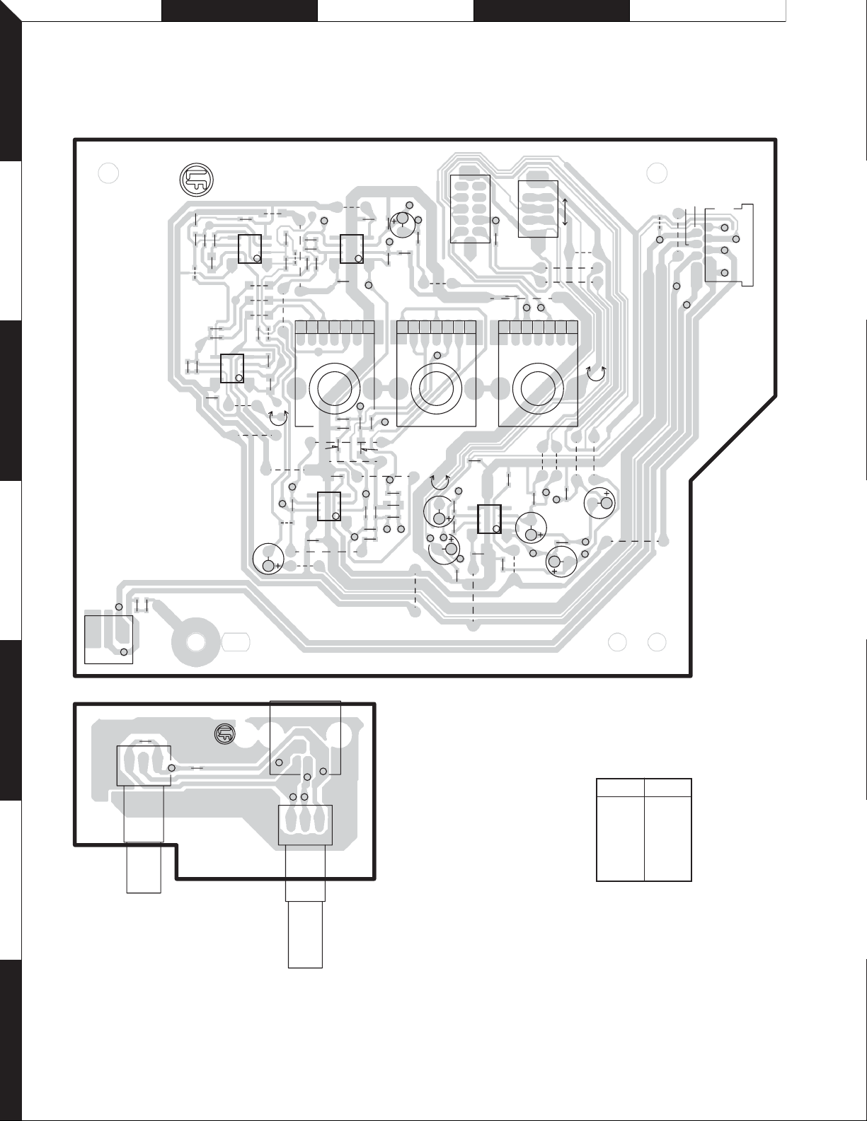
PC BOARD (FOIL SIDE VIEW)
PREAMPLIFIER UNIT X08-4180-1x A/2 (J76-0068-02)
S2
OFF
10
TP24
R111
C108
41
TP26
TP25
BASS BOOST
TP45
R122
R121
C116
TP38
C117
C118
R126
R112
TP37
TP40
C107
R113
W10
TP42
1
46352241365
LOW PASS
R125
C119
R124
TP41
TP23
R110
C101
TP15
W3
W16
VR2
50Hz
TP12
C102
TP36
200Hz
51
6
I.S.F
R102
TP11
R101
58
IC11
R103
C104
TP14
R104
W2
25Hz
TP27
58
C201
R202
R203
R201
C109
VR3
R119
C115
R120
C123
58
IC13
C122
TP39
W22
IC12
W13
14
R123
C203
C202
R208
R206
R204
58
2
W252
R212
R210
C208
R211
3
C207
IC14
C204
W256
W255
W254
41
58
IC15
W203
W202
4
C126
R129
TP48
W52
41
R207
W204
W251
R209
C206
C205
18dB
0dB
W201
TP43
TP44
C121
W151
W21
R205
W253
W14
C120
W6
W5
15Hz
TP20
R109
R127
TP22
1
463 52
INPUT SENS
C103
C106
41
R108
W4
4
6
I.N.V
W15
R107
S1
TP18
1
3
TP21
W12
TP17
W11
TP13
R106
C124
ONOFF
R105
W9
VR1
5V
TP16
TP19
TP1
W20
W18
W17
200mV
W8
C105
W7
CN2
3
1
TP49
W51
+15V
W19
TP5
LED
ISO GND 1
ISO GND 2
SIG1
17
82
TP7
TP2
-15V
TP8
DGND
CN1
TP4
SIG2
TP3
X08 B/2
5
6
7
Refer to the schematic diagram for the values of resistors and capacitors.
R623
VR62
1
3
FREQUENCY
TP63
R62
TP61
TP60
3
2
4
TP65
TP64
1
J1
VR61
4
X08-4180-1x
Ref. No. Address
IC11 4N
IC12 2M
TP62
1
IC13 4M
IC14 2L
IC15 3L
BOOST
LEVEL
6