Kenwood KAC-6202 Service manual

POWER AMPLIFIER
KAC-6202
SERVICE MANUAL
© 2005-5 PRINTED IN JAPAN
B53-0286-00 (N) 1708
KAC-6202
KAC-6202
(E type,M type)
Stereo/
Bridgeable
Powe
MAXIMUMPOWER
(K type)
Amplifie
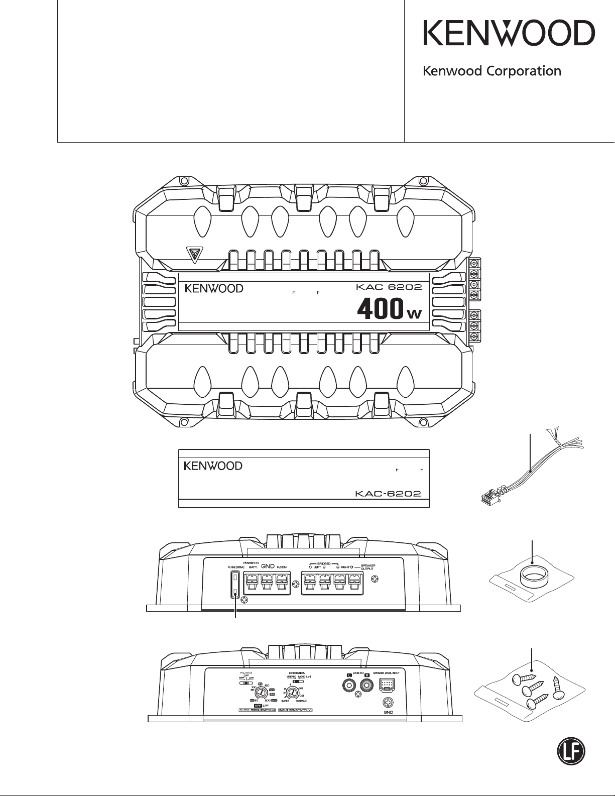
Connecting cord assy
(E30-6145-05)
Fuse
(F52-0014-05)
Stereo/
Bridgeable
Powe
Amplifie
190mm
Accessory
(W01-1607-05)
Screw set
(N99-1587-05)
This product uses Lead Free solder.

KAC-6202
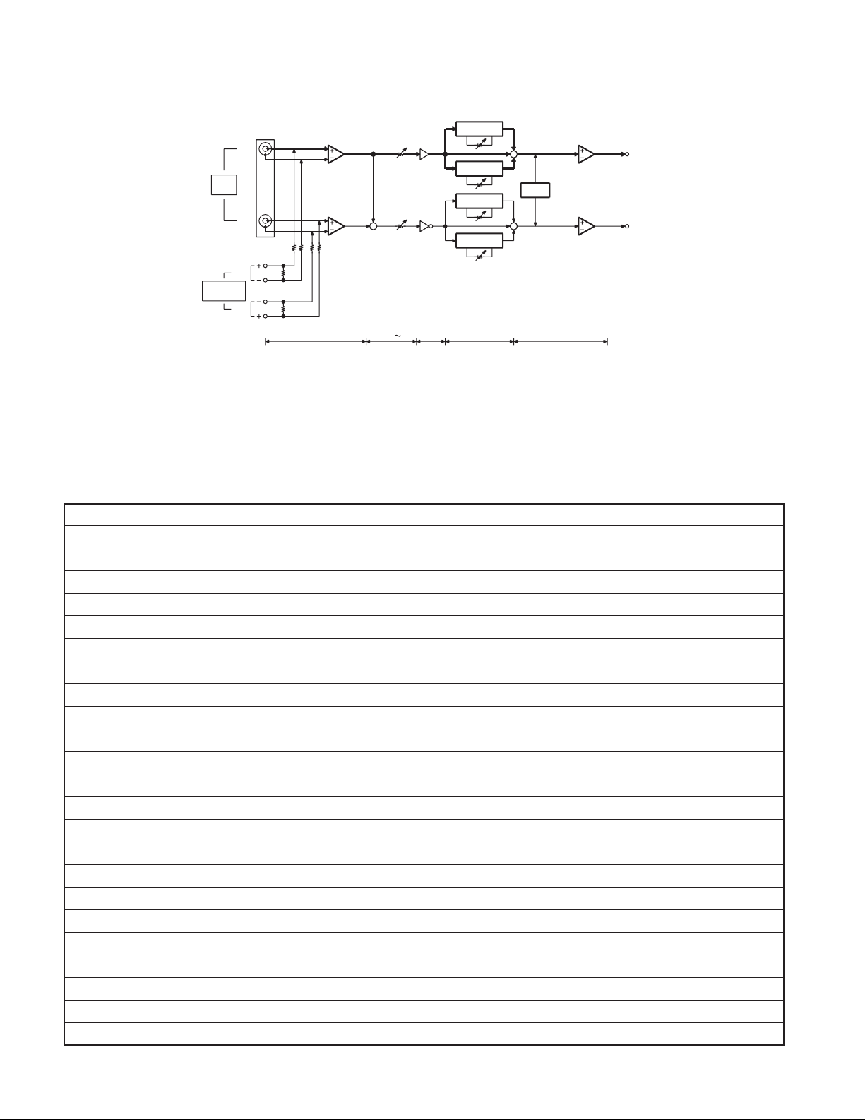
BLOCK DIAGRAM
RCA
LINE
IN
SPEAKER
IN
Rch
Lch
Lch
Rch
X09-590
+6dB
ISOLATION
AMP
6dB 6dB-27 0dB(LPF:+6dB) 26dB
INPUT OUTPUT
SW
ST/MONO
+6dB
PHASE
INVERT
HPF
LPF(+6dB)
LPF(+6dB)
HPF
MUTE
SW
HPF/OFF/LPF
L
P. AMP
R
COMPONENTS DESCRIPTION
● AUDIO UNIT (X09-5900-10)
Ref. No. Application / Function Operation / Condition / Compatibility
IC1 Buffer amplifier +6dB, low-impedance conversion
IC2 Isolation amplifier Common mode noise filtering
IC3 Buffer amplifier +6dB,Rch reversal
IC4 Reversal buffer amplifier +6dB, reversal amplifier
IC5,6 HPF/LPF Fitter with variable cutoff
IC7 DC/DC converter Oscillation and control of DC/DC converter
Q1,2 Switching Transistor for ON/OFF control of latter step driver
Q3~6 Drive transistor FET driver for the latter steps
Q7,8 Switching FET Switching FET for the secondary power supply
Q201,202 For muting Transistor for muting B-class step
Q203~206 Differential amplifying transistor Transistor for first step differentiation amplification
Q207~210 Differential amplifying transistor Transistor for second step differentiation amplification
Q211,212 Current mirror load Current mirror load of second step differentiation
Q213,214 Temperature compensating transistor For prevention of thermal-runaway of the final transistor
Q215~218 Over current protection Transistor protection against excess current
Q219~222 Power amplification First step of Darlington power amplification
Q223~226 Power amplification Second step of Darlington power amplification
Q501,502 Constant voltage stabilization Transistor for constant voltage stabilization
Q601,602 Switching Transistor for mute ON/OFF control for B-class step
Q603,604 Switching Transistor for mute control for B-class step
Q605 Switching Transistor for DC protection circuit latch
Q606 Switching For DC protection latch ON control
Q607,608 Drive transistor For DC protection circuit driving
2

KAC-6202
COMPONENTS DESCRIPTION
Ref. No. Application / Function Operation / Condition / Compatibility
Q609 Switching For PULL-DOWN of DC/DC converter 2 pin
Q610~614 Switching Transistor for power supply circuit ON/OFF control
Q615 Switching Transistor for mute ON/OFF control for latter steps
D1 Circuit protection diode For circuit protection at reverse connection of power supply cord
D4~7 Switching Backflow prevention diode
D8,9 Rectifying diode Rectification on the secondary power supply side
D101~103 Static protection diode For circuit protection against static
D201 Switching Backflow prevention diode
D202,203 Operation stabilizer diode Contains thermal fluctuation of transistor Vbe of second step differentiation
D204,205 Current mirror load Current mirror circuit load
D206~211 Switching Backflow prevention diode
D501 Indicator LED Indicator for behavior visual check
D601 Bias diode Backflow prevention diode
D602,606 Switching Backflow prevention diode
D603 Level shifter For DC protection circuit bias
D604 Switching For turning operation off at P-CON momentary power down
D605 Switching For turning off operation at BATT excess voltage and for circuit protection
D607 Level shifter For bias of the mute control circuit
D608~612 Switching Backflow prevention diode
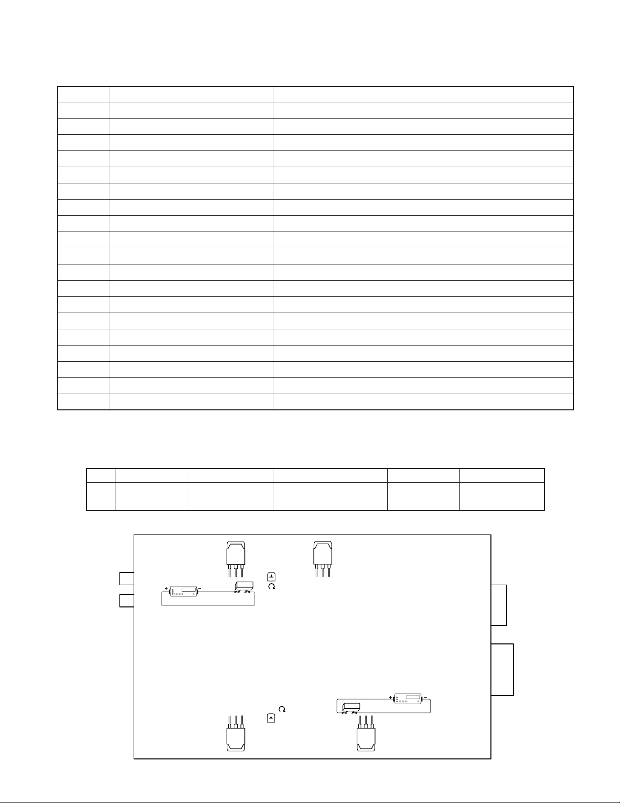
ADJUSTMENT
No. Item Alignment point Method Align for Note
1
IDLE VR3 (Lch) Connect a DC voltmeter
CURRENT VR4 (Rch) between emitter resister 5 minutes
Q223
R278
Q226
Lch 2.5mV
DC voltmeter
Q225
Q224
R277
VR3Lch
MIN MAX
MIN MAX
VR4
Rch
2.5mV
Rch 2.5mV
DC voltmeter
After Power on
3

A B C D E
7
5
W
Q609
KAC-6202
1
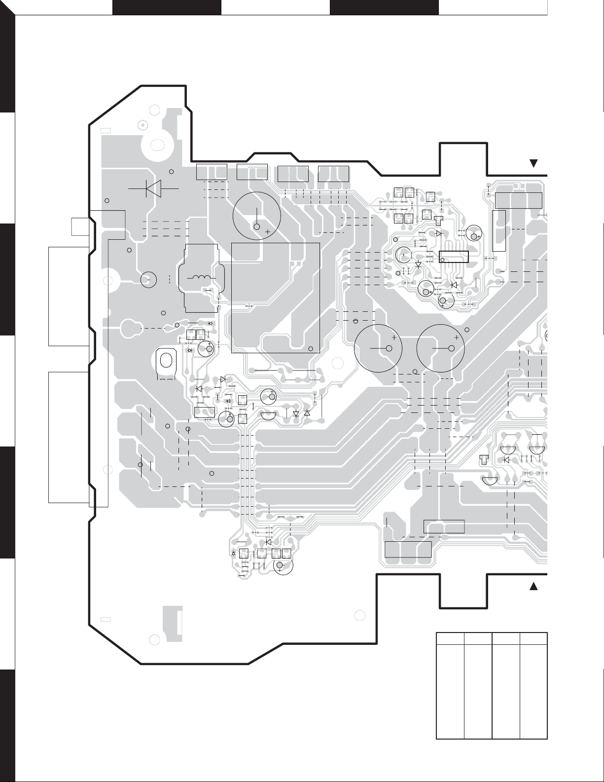
PC BOARD (FOIL SIDE VIEW)
AUDIO UNIT
X09-5900-10
(J76-0088-11)
R281
R282
C11
W208
C239C240
GND
W202
W203
W204
P1
L-OUT
GND
W207
P-CON
W201
SDG SDG
Q8
L1
TH1
D604
R621
Q612
BE
BE
Q611
R624
W422
D605
C607
R622
D606
R623
R625
R636
BE
Q610
W421
GND
W205
W206
W199
GND
W197
W200
W198
R626
R627
D608
R628
C608
W419
W420
R630
D607
W418
R629
D603
R613
C613
R614
Q613
BE
R631
R638
Q605
C604
W188
W189
W190
W195
W196
W191
W192
W193
W194
BE
W417
BE
Q7
R632
Q614
W416
D602
R611
C602
2
D1
BATT-F
BATT
3
J3
4
R-OUT
1234 56 7
5
Q615
BE
R612
C609
W413
W149
R615
BE
W414
W415
Q607
BE
Q606
R280
C603
W187
C10
R633
BE
D9
D8
W186
W185
W184
W181
W183
W182
W179
W178
W177
W180
W170
W171
W172
W173
W174
L3
W175
W176
-B
GND
R24R25
C6
C5
W411
R634
D610
D609
R279
W209
Q608
R23
R22
THERMAL
R287
R21
R20
Q5
BE
R19
R18
BE
Q4
C4
W409
THERMAL
C8
W167
W168
Q226
BE
W410
GND
W165
BE
Q3 Q6
W407
R3
R8
W408
C3
W169
R10
R14
R26
R15
R7
W406
D6
W163
EB
Q2
BE
W403
BE
D7
Q1
W401
D4
W402
C9
R1
16 9
IC7
18
R11
R6
R4
W404
R2
W405
C12
C7
W161
W159
W160
W158
W162
W156
W164
W166
W157
R278
D5
R9
W400
+B
C1
C2
D211
W398
R275
W395
EB
Q222
Q223
W150
W152
W154
C236 C238
Q216
BEBE
D209
W155
W153
W145
W146
R268
R266
R284
W151
R272
BE
C606
Q218
R28
R274
W39
W148
R270
6
X09-5900-10
Ref. No. Address
IC1 3I
IC2 3H
IC3 4I
IC4 4I
IC5 5H
IC6 5I
7
Refer to the schematic diagram for the values of
resistors and capacitors.
IC7 3E
Q1 2D
Ref. No. Address
Q2 2D
Q3 3D
Q4 3D
Q5 2D
Q6 2D
Q7 2C
Q8 2B
Q201 4H
4
 Loading...