

Page 1
144MHz FM TRANSCEIVER
TH-K2AT/K2E/K2ET
SERVICE MANUAL
© 2003-8 PRINTED IN JAPAN
B51-8658-00 (S) 836
Helical Antenna
(T90-1018-25)
Knob
(PTT/LAMP/MON)
(K29-9274-03)
Key top (16key)
(K29-9272-02)
Knob (ENC)
(K29-5159-03)
Knob (VOL)
(K29-5150-03)
Front glass
(B10-2746-03)
Cap
(SP/MIC/DC IN)
(B09-0675-03)
Cabinet assy
(16key)
(A02-3819-23)
Helical Antenna
(T90-1018-25)
Knob
(PTT/LAMP/MON)
(K29-9274-03)
Key top (4key)
(K29-9276-02)
Knob (ENC)
(K29-5159-03)
Knob (VOL)
(K29-5150-03)
Front glass
(B10-2746-03)
Cap
(SP/MIC/DC IN)
(B09-0675-03)
Cabinet assy
(4key)
(A02-3818-23)
TH-K2AT/K2ET TH-K2E
CONTENTS
DISASSEMBLY FOR REPAIR ...................................2
CIRCUIT DESCRIPTION ............................................ 6
SEMICONDUCTOR DATA ...................................... 14
COMPONENTS DESCRIPTION ..............................15
PARTS LIST.............................................................17
EXPLODED VIEW....................................................23
PACKING ................................................................. 25
ADJUSTMENT ........................................................ 27
TERMINAL FUNCTION........................................... 43
PC BOARD
TX-RX UNIT (X57-674X-XX) (A/3) ................... 44
TX-RX UNIT (X57-674X-XX) (B/3),(C/3) ..........48
SCHEMATIC DIAGRAM..........................................50
LEVEL DIAGRAM.................................................... 55
BLOCK DIAGRAM................................................... 56
BC-21 (WALL CHARGER) .......................................58
PB-43N (Ni-MH BATTERY PACK) ..........................58
BT-14 (BATTERY CASE) ......................................... 59
PG-4Y (PROGRAMMING INTERFACE CABLE) .....59
MCP-1A (MEMORY CONTROL PROGRAM) ......... 59
SPECIFICATIONS................................. BACK COVER
Page 2
TH-K2AT/K2E/K2ET
CN2
CN9
CN6
x
x
c
c
v
m
b
,
,
.
ç
√
µ
∫
∫
∫
∫
∫
Ω
/
∫
≈
~
≤
n
z
TX-RX unit (B/3)
TX-RX unit (C/3)
TX-RX unit (A/3)
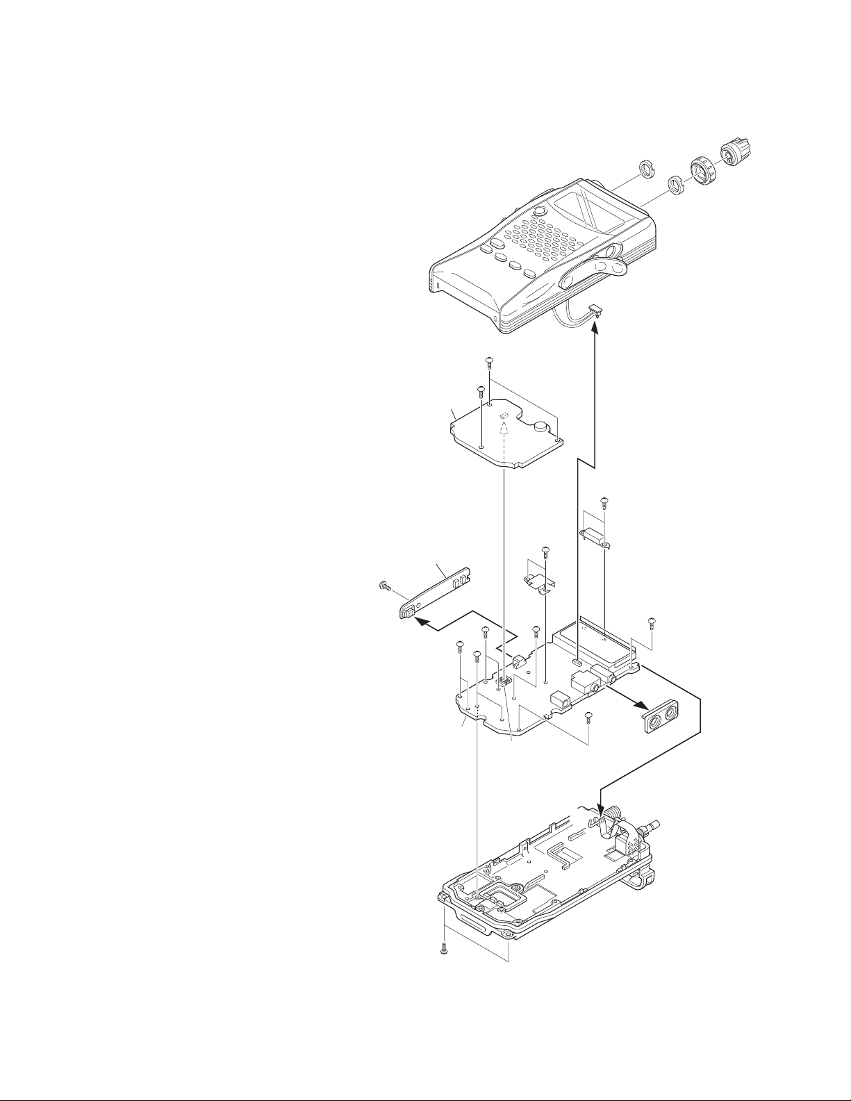
DISASSEMBLY FOR REPAIR
How to remove the case assembly from the chassis
1. Remove two screws (z) holding the chassis.
2. Pull out two knobs (
3. Pull out the SP and MIC parts of the cap from jacks (
4. Turn the unit over with the bottom of the chassis facing
upwards, and remove the chassis (
assembly (
5. Remove the speaker lead (
the TX-RX PC board (TX-RX unit A/3).
b
).
) and remove two round nuts (c).
x
) from the case
n
) from the connector (CN2) of
m
v
).
How to remove the PC board
■ Numeric key PC board (TX-RX unit B/3)
1. Remove three screws (,) on the numeric key PC board.
2. Lift the numeric key PC board and remove it from the
■ PTT PC board (TX-RX unit C/3)
3. Remove one screw on the PTT PC board (/).
4. Pull the PTT PC board to the left and remove it from the
■ TX-RX PC board (TX-RX unit A/3)
5. Remove the SP/MIC jack cover (≈).
6. Remove two screws (
7. Remove two screws (
8. Remove eight screws (
9. Absorb solder from the antenna terminal (
Note: Do not melt the shadow plate (
10.Remove the TX-RX PC board from the chassis, then remove
connector (CN9) of the TX-RX PC board (
.
).
connector (CN6) of the TX-RX PC board (TX-RX unit A/3)
(
Ω
).
) holding the shield
ç
cover (antenna terminal section).
) holding the shield
√
cover (final amplifier section).
board.
with a solder absorber.
) on the TX-RX PC
∫
µ
moving the tip of the solder absorber close
to the antenna terminal.
the encoder volume FPC (
of the TX-RX PC board.
) from the flat cable connector
≤
~
) when
)
2
Page 3
TH-K2AT/K2E/K2ET
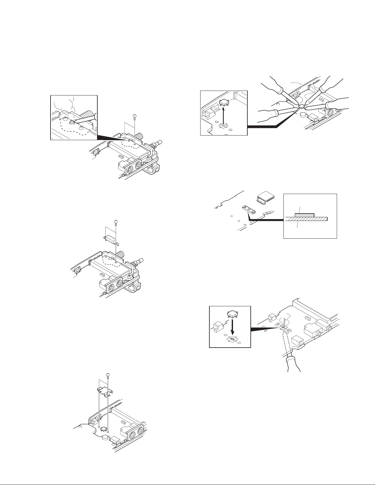
DISASSEMBLY FOR REPAIR
Soldering the antenna terminal
1. With the shield cover removed from the antenna terminal
section, install two screws on the PC board and bring the
PC board into contact with the chassis (
2. Solder the antenna terminal with a soldering iron (
z
).
).
x
x
z
3. Remove the two screws installed in step 1 above, and install
the two screws again on the PC board together with the
shield cover (
c
).
c
4. Apply the tips of soldering irons to all the four pins of the final
FET at the same time (
the final FET (
). (Two persons should be required to do this.)
v
v
5. Remove all PC boards from the chassis.
6. Confirm that there is no space between the radiation plate
installed on the foil side of the TX-RX PC board (TX-RX unit
A/3) and the PC board (
the radiation plate and PC board, eliminate it by applying
the tip of the soldering iron to the radiation plate.
), heat them sufficiently, and remove
c
c
). If there is any space between
b
b
Radiation plate
TX-RX PC board
Replacing the final FET (Q12)
1. Remove the two screws holding the shield cover of the
final FET section (
2. Remove solder from the shield cover completely with a
solder absorber. (E and E3 types only)
3. Remove the shield cover (
z
).
).
x
z
x
7. Apply the tip of the soldering iron to the installation side of the
radiation plate of the TX-RX PC board, put a little amount of
solder to the radiation plate that is seen through a square hole
in the final FET installation section and melt the solder (
8. When the solder in step 7 is melted, place the final FET on
the PC board by aligning it with the silk of the final FET
installation section of the PC board (
m
).
n
).
m
n
9. Release the soldering iron and confirm that the final FET
and radiation plate have been soldered.
10.Solder the four pins of the final FET with the soldering iron.
11.Install all the PC boards.
12.Reinstall the shield cover removed in step 3 above in its
original position and install two screws.
13.Solder the shield cover to the PC board. (E and E3 types
only)
14.
Install the chassis on the case assembly and assemble them.
15.Readjust transmission power.
Note: Since the FET is sensitive to static electricity, always
wear a grounding band. Use a highly insulated ceramic
heater solder iron.
3
Page 4
TH-K2AT/K2E/K2ET
DISASSEMBLY FOR REPAIR
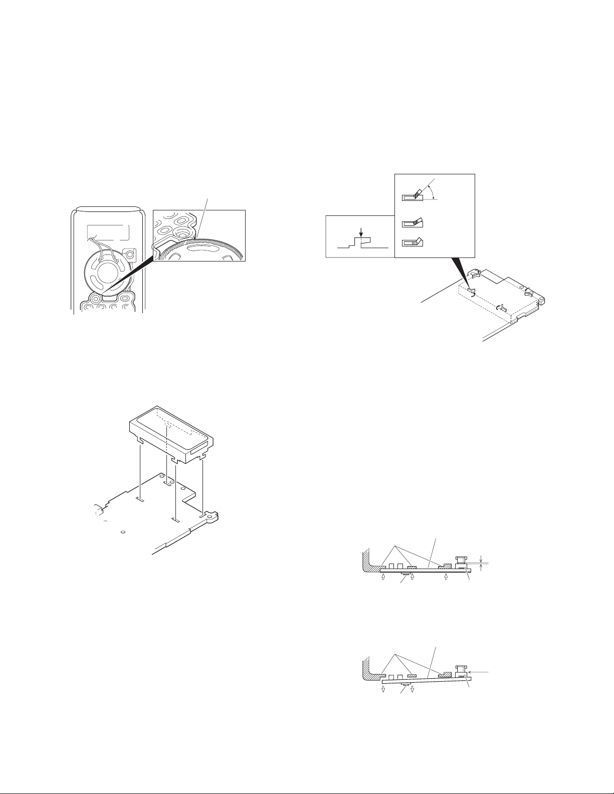
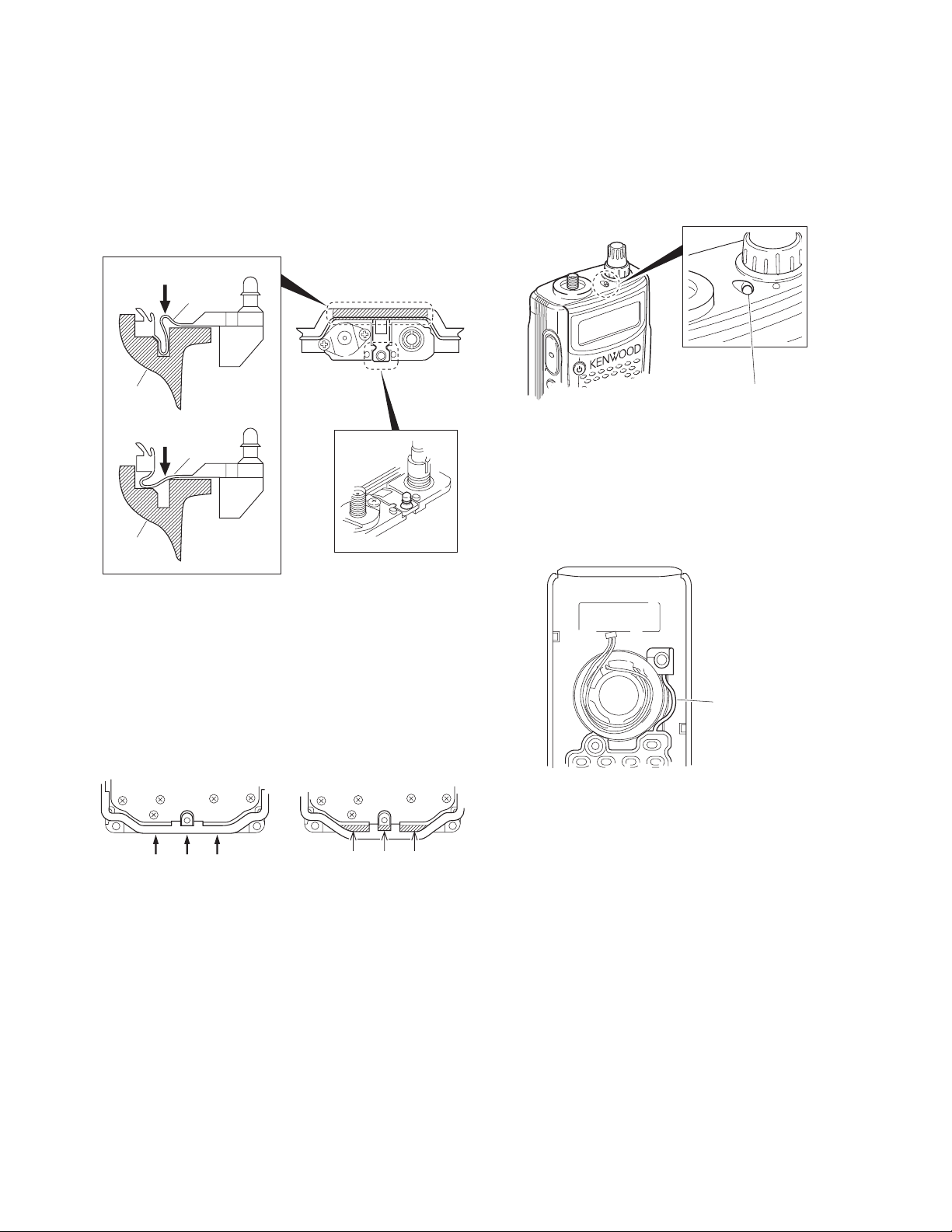
Special care and attention required for assembly
1. Gluing to the key top (MIC element section)
You must also glue on the speaker storage area and heap
the glue up until wealthy glued on the speaker storage area
and the key top for waterproofing the MIC element side of
the key top. (Fig. 1)
Heap the glue up until wealthy glued on the speaker
storage area and the key top (MIC element section).
Fig. 1
2.
Bending the LCD hardware fixture (J21-8456-03) tabs
(1)Insert the tabs of the LCD hardware fixture into four holes
in the LCD installing position of the TX-RX PCB (TX-RX unit
A/3). (Fig. 2)
Fig. 2
(2)By pressing the LCD hardware fixture from the component
side of the TX-RX PCB, you must bent all 4 tabs of the LCD
hardware fixture being visible from the foil side until the
bases of each tabs are folded at least 45 degrees (Fig. 3). If
the bending angle of the tabs of the LCD hardware fixture
is less than 45 degrees, a display error may occur.
Min 45
degrees
Bending position
NG
NG
Fig. 3
3. PTT PCB (TX-RX unit C/3) installation procedure
Installing the PTT PCB on the TX-RX PCB and chassis are
as follows:
(1)Insert the PTT PCB connector (CN7) into the TX-RX PCB
connector (CN6) lightly.
(2)Push three parts of the PTT PCB to contact tightly with the
chassis. There may be a small gap between the connectors.
(Fig. 4)
Note: A double-side adhesive tape (J99-0376-04) is used
behind the PTT switch. When reassembling the PTT
PCB to the chassis, press the PTT PCB (under the PTT
switch) so that the tape hold the PCB and chassis
securely.
Chassis
OK
PTT switch
Push three parts of the PTT PCB
to contact tightly with the chassis.
PTT PCB (C/3)
CN6
A bit
clearance
CN7
Chassis
NG
PTT switch
PTT PCB (C/3)
CN6
No
clearance
CN7
Fig. 4
(3)Tighten one screw in the PTT PCB.
4
Page 5
TH-K2AT/K2E/K2ET
LAMP
LO
W
PTT
DISASSEMBLY FOR REPAIR
4. Packing (G53-1572-02) TX/BUSY lamp installation
procedure
(1)To assure waterproofing, install the packing in the chassis
groove as shown in Fig. 5. (
(2)Install the packing TX/BUSY lamp section on the chassis.
(
)
x
z
OK
Packing
Chassis
NG
Packing
Chassis
z
)
x
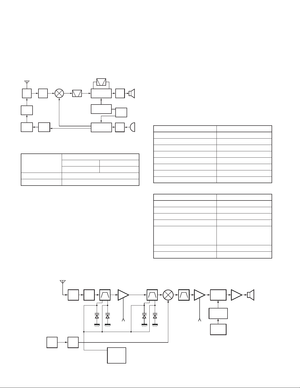
Cautions for installing the chassis on the case assembly
6.
(1)Verify that the packing (G53-1572-02) TX/BUSY lamp section
is has been past through the hole in the illumination guide
section on the top of the case assembly. (Fig. 7)
The packing TX/BUSY lamp section is has
been past through the hole in the illumination
guide section on the top of the case assembly.
Fig. 7
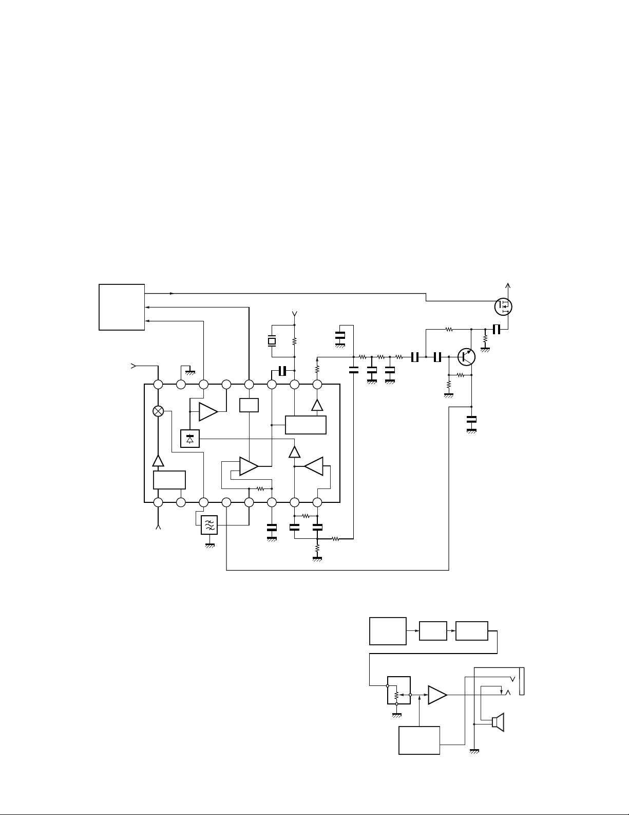
(2)Align the speaker lead as shown fig.8. Do not place the
leads over the key top section, LCD section or SP/MIC/DC
IN cap section.
Fig. 5
5.
Packing (G53-1572-02) bottom installation procedure
(1)Before installing the numeric key PCB (TX-RX unit B/3) on
the chassis, push three parts of the packing to contact tightly
with the chassis as shown in Fig. 6. If the packing is not in
contact with the chassis, there may be a gap between the
transceiver bottom case assembly and the battery, and
water may enter through the gap.
OK NG
Push three parts of the packing to
contact tightly with the chassis.
Clearance NG
Fig. 6
Do not fix this part of the
key top to the rib of the
case assembly.
Fig. 8
7.
Cautions for installing the key top on the case assembly
(1)Install the key top keypad section and the power switch
section on the rib of the case assembly.
(2)Do not fix the part between the key top keypad section and
the power switch section to the rib of the case assembly,
but install it as shown in Fig. 8.
5
Page 6
TH-K2AT/K2E/K2ET
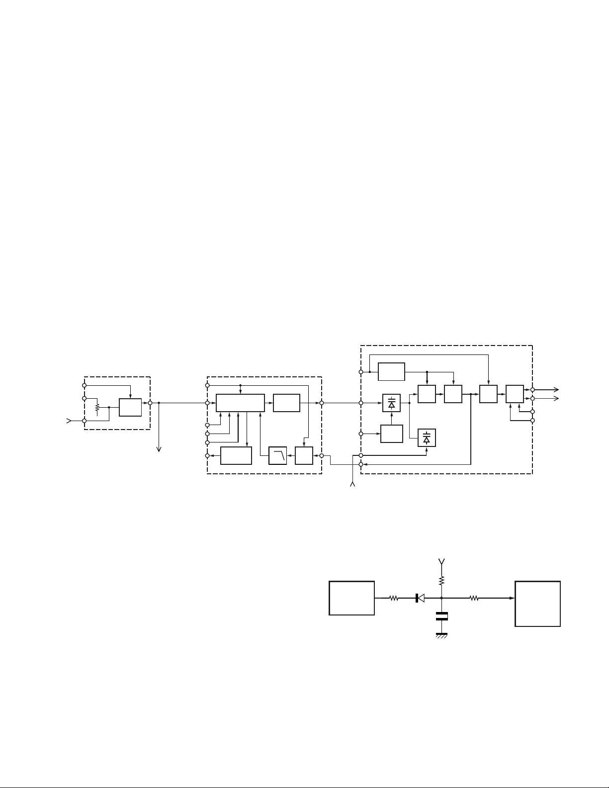
CIRCUIT DESCRIPTION
Frequency Configuration
The frequency configuration is shown in Figure 1 and
Table 1.
136.000~173.995MHz(K,K2,M,M2)
RX :
144.000~145.995MHz(E,E3)
TX :
ANT
ANT
SW
FINAL
DRIVE
144.000~147.995MHz(K,K2)
136.000~173.995MHz(M,M2)
144.000~145.995MHz(E,E3)
1st MIX
RF
AMP
PRE
DRIVE
144.000~147.995MHz(K,K2)
136.000~173.995MHz(M,M2)
144.000~145.995MHz(E,E3)
38.85MHz
174.850~212.845MHz
(K,K2,M,M2)
182.850~184.845MHz
(E,E3)
MCF
450kHz
CF
MIX, IF,
DET
Tripler
x 3
PLL
VCO
38.4MHz
AF
AMP
TCXO
MIC
AMP
SP
12.8MHz
MIC
Fig. 1 Frequency configuration
Double super heterodyne
Reception method 1st IF Frequency 38.85MHz (Upper)
2nd IF Frequency 450kHz (Lower)
Transmission method
VCO direct oscillation amplification
Modulation Variable reactance phase modulation
Table 1 Basic configuration
Receiver System
■ Front End
The received signal from the antenna passes through a lowpass filter and then through a transmission/reception switching
circuit (antenna switch) and enters the band-pass filter (L40,
L41, L38).
The signal passing through the band-pass filter (L40, L41,
L38) is amplified by with an RF amplifier (Q17), passes through
a band-pass filter (L32, L35) and enters the first mixer (Q16).
These band-pass filters are tuned to a desired frequency
by varicaps (D21, D20, D19, D18).
A tuning voltage corresponding to the desired signal is
applied to each varicap through the BPF/APC terminal (pin 6)
of the MPU (IC8) to tune to the receive frequency.
■ First Mixer
The received signal passing through the band-pass filter
(L32, L35) is mixed with the first local signal generated by the
VCO by the first mixer (Q16) to produce a first IF signal (38.85
MHz) (Upper heterodyne).
The first IF signal passes through a MCF (Monolithic crystal
filter: XF1) to remove unwanted components.
The first IF signal passing through the MCF (XF1) is amplified
by an IF amplifier (Q24) and the resulting signal enters the FM
IC (IC3).
Item Rating
Nominal center frequency (fo) 38.85MHz
Pass bandwidth ±6.0kHz or more at 3dB
Attenuation bandwidth ±25kHz or less at 35dB
Ultimate attenuation 70dB or more (fo –910 kHz)
Spurious response 40dB or more (fo +1MHz)
Ripple 1dB or less
Insertion loss 4dB or less
Terminating impedance 610Ω ±5% // 3pF ±0.5pF
Table 2 MCF (L71-0619-05) characteristics (TX-RX unit XF1)
Item Rating
Nominal center frequency (fo) 450kHz
3dB bandwidth ±6.5kHz or more
50dB bandwidth ±15.5kHz or less
Ripple 2dB or less (fo ±6.5kHz)
55dB or more
Guaranteed attenuation (fo ±18kHz to ±33kHz)
50dB or more (fo ±100kHz)
Insertion loss 4dB or less
I/O matching impedance 1.5kΩ
Table 3 Ceramic filter (L72-0968-05) characteristics (TX-RX unit CF1)
ANT
BPF
L41,L40,L38
ANT
SW
Tuning voltage
PLL
LV
LPF
VCO
6
RF AMP
Q17
D20D21
6
BPF/APC
MPU
IC8
Fig. 2 Receiver section configuration
D19
BPF
L32,L35
MIXER
D18
Q16
MCF
XF1
38.85MHz
1st Local OSC
(PLL)
IF AMP
Q24
5R5R
FM IC
IC3
IF AMP,
DET
2nd Local OSC
Tripler
x 3
TCXO
12.8MHz
AF AMP
IC6
Q23
X1
SP
Page 7
TH-K2AT/K2E/K2ET
CIRCUIT DESCRIPTION
■ IF Circuit
The first IF signal (38.85 MHz) amplified by the IF amplifier (Q24)
and the second IF signal (38.4 MHz) generated by tripling the 12.8
MHz reference oscillator frequency of the TCXO (X1) by Q23, are
mixed in the FM IC to produce a second IF signal (450 kHz) (Lower
heterodyne).
The second IF signal passes through a ceramic filter (CF1)
to remove unwanted components.
The second IF signal passing through the ceramic filter (CF1)
passes through the IF amplifier in the FM IC again and is
detected to produced an audio signal.
■ Squelch and Mute Circuit
A noise component is obtained by passing FM detection
output (FM IC pin 9) through an operational amplifier in the
9
AFM
49
IC8
MPU
1st IF input
(38.85MHz)
SM
SQ
IC3
FM IC
2nd local OSC
(38.4MHz)
SMV
48
SQV
16 15 14 13 12 11 10 9
MIX
Noise
comp
Rectifier
Buffer
Local
OSC
1 2 3 4 5 6 7 8
CF1
450kHz
RSSI
IF AMP
5R
CD1
Quadrature
detector
C173 C174
Inverter
R135
R125
AF OUT
Noise
AMP
AMP
FM IC and band-pass filter consisting of R125, R126, R135,
C173, C174. The noise component is rectified in the FM IC to
produce a DC voltage, which is output from the N-REC terminal
(pin 14) of the FM IC as squelch voltage.
The squelch voltage enters the SQ terminal (pin 48) of the
MPU (IC8) and is compared with the reference voltage preset
in the MPU to control audio signal ON/OFF.
When "L" is output from the AFM terminal (pin 9) of the MPU,
the AF mute switch (Q20) is activated to mute the audio signal.
■ S Meter Circuit
The S meter voltage is output from the RSSI terminal (pin
12) of the FM IC (IC3) and input to the SM terminal (pin 49) of
the MPU. Then the voltage is converted from analog to digital
in the MPU to control the S meter display on the LCD.
VOL IN
Q20
AF MUTE
SWITCH
Q21
AF FILTER
LPF
R126
5R
Fig. 3 IF, Squelch, Mute and S meter circuit
■ AF Amplifier
The detected audio signal passes through an AF filter (Q21)
and enters an AF mute switch (Q20).
After passing through the AF mute switch (Q20), the signal
passes through an AF volume (VR201) and is amplified to a
specified output level with an AF amplifier (IC6).
The audio signal amplified with the AF amplifier (IC6) is
output through an internal speaker or an external speaker
jack (J4).
The beep tone and the DTMF signal are output from the
DTMF/BEEP terminal (pin 40) of the MPU (IC8), enters the AF
amplifier (IC6) and is output as a monitor tone.
IC3
FM IC
9
AF OUT
VR201
AF VOLUME
40
DTMF/BEEP
IC8
MPU
Q21
AF
FILTER
IC6
AF AMP
REM
46
Q20
AF MUTE
SWITCH
SPG
REM/TXD
SPK
AFO
Fig. 4 AF amplifier
J4
SP JACK
SP
7
Page 8
TH-K2AT/K2E/K2ET
CIRCUIT DESCRIPTION
Transmitter System
■ Microphone Amplifier Circuit
The audio signal from the microphone passes through a
high-pass filter (IC5) and enters a microphone amplifier (IC16).
The signal passes through a pre-emphasis circuit, limiter
amplifier and splatter filter inside the microphone amplifier.
The splatter filter will remove distortion outside the audio band.
IC16
MIC AMP
MIC IC5
61
HPF
emphasis
Fig. 5 Microphone amplifier circuit
■ Modulation Circuit
The audio signal amplified by the microphone amplifier
(IC16) passes through a semi-fixed volume (VR5) for
modulation adjustment, and goes to the VCO modulation
varicap (D6) for variable reactance phase modulation.
■ Drive and Final Circuit
The output signal from VCO (Q1) passes through an RF
amplifier (Q2, Q5, Q9) and drive amplifier (Q10, Q11), and is
amplified by a power amplifier (Q12).
■ Transmission/Reception Switching Circuit
The signal amplified by the power amplifier (Q12) passes
through a transmission/reception switching circuit and a lowpass filter, and is fed to the antenna.
Q11
Q10
Pre-
Limiter
VCO
Splatter
filter
Q12
The transmission/reception switching circuit consists of D10,
L19, D12 and D13. These diodes are turned ON in transmit
mode and OFF in receive mode to switch signals.
MIC
IC5
HPF
AMP
DRIVE AMP
Q10
DRIVE AMP
IC16
MIC
Q11
VR5
MAX DEV
Q12
POWER AMP
Q1
VCO
Q2
RF AMP
D10,L19
D12,D13
ANT
SW
RF AMP
LPF
Q5
ANT
Q9
RF AMP
Fig. 6 Modulation, Drive, Final and
Transmission/reception switching circuit
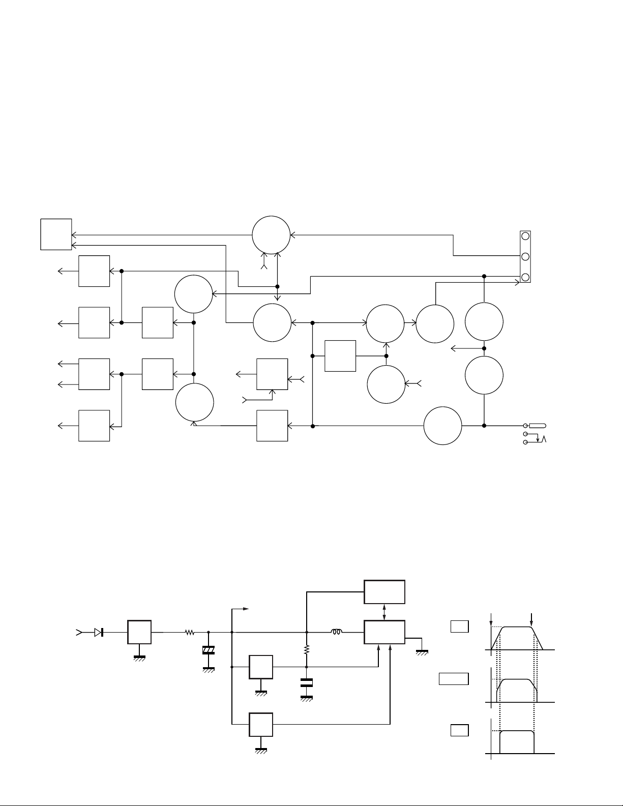
■ APC Circuit
The APC (Automatic Power Control) circuit is used to obtain
a stable transmission power and controls transmission output
by detecting the drain current of Q11 and Q12.
The transmission output can be changed in three levels:
High, Mid, and Low.
The reference voltage is output from the BPF/APC terminal
(pin 6) of the MPU (IC8) and the detection voltage generated by
R70, R71 and R72 are fed to the APC differential amplifier (IC2).
The voltage in proportion to the difference between
reference voltage and detection voltage is output from the
BOUT terminal (pin 7) of IC2 as an APC voltage.
ANT
D10
LPF
L19
D13
RX
Q55
–t
TH1
+
51
THERM
7
KAPC
6
BPF/APC
IC8
MPU
FINAL
16
Q58
D12
VGG
Q15
5T
R72
R71
R70
B
Q13
B
8
Fig. 7 APC and Temperature protection circuit
1
2
3
4
VDD
APC AMP
AOUT
A–IN
A+IN
GND
IC2
BOUT
B–IN
B+IN
8
V+
7
6
5
Q14
Page 9
TH-K2AT/K2E/K2ET
Fo/LD
PLL LD
IC8
MPU
IC1
PLL IC
R32
D16
C40
R35
14
102
5C
CIRCUIT DESCRIPTION
The APC voltage controls the gate voltage of Q11 and Q12,
and keeps transmission output stable.
The MPU detects power supply voltage and controls Q58
by transmission power supply voltage and transmission power.
For example, if the power supply voltage during transmission,
is equal to or higher than approx. 10.5 V and if power is at Mid
or Low level, the APC voltage level applied to Q12 is reduced
by Q58.
■ Temperature Protection Circuit
To prevent thermal destruction of the power amplifier (Q12),
this circuit reduces APC voltage when Q12 temperature rises.
The MPU (IC8) detects temperature with a thermistor (TH1)
and controls reference voltage to the APC circuit.
PLL System
■ PLL Circuit
A reference frequency of 5 kHz or 6.25 kHz is produced by
dividing the 12.8 MHz reference frequency of the TCXO (X1)
with PLL IC (IC1). Comparison frequency is produced by
TO
5C
5/0V
5MS
5/0V
TCXO
VR1
VC
X1
TCXO
12.8MHz
12.8MHz
IF
5C
5/0V
CLOCK
DATA
Fo/LD
PLL
IC1
PLL IC
LE
Rectifier
LOOP
FILTER
LPF Q6
amplifying VCO output with an RF amplifier (Q6) and dividing
it with the PLL IC.
The PLL synthesizer with 5 kHz and 6.25 kHz step is
configured by comparing phases of the reference frequency
and comparison frequency.
The phase difference between reference frequency and
comparison frequency passes through a charge pump in the
PLL IC, then ripples are removed with a loop filter with lowrange passing characteristics to produce VCO control voltage
(lock voltage).
■ VCO Circuit
The VCO produces a desired frequency directly with a
Colpits oscillation circuit containing an oscillation transistor (Q1)
used for both transmission and reception.
The VCO control voltage is applied to varicap (D1, D2) to
produce a desired frequency.
The SHIFT terminal (pin 113) of the MPU (IC8) goes "H"
during reception, and the shift control switch (Q3) is turned
ON to change oscillation frequency.
VCO
Q4
Ripple
D1,D2
Q3
SHIFT
Filter
SW
Q1
OSC
MOD
Q2
Buff
Amp
Q5
Amp
RF
RF
Amp
LV
1~5V
5C
5/0V
SHIFT
H/L
D8,D9
SW
TX
RX
5T 5/0V
5R 5/0V
Fig. 8 PLL and VCO circuit
■ Unlock Detection Circuit
When the PLL is unlocked, the waveform of the pulse
output from the Fo/LD terminal (pin 14) of the PLL IC (IC1) is
rectified with R32, D16, R35 and C40, and the Fo/LD terminal
is made “L” level. The voltage at the Fo/LD terminal is
detected by the MPU to control transmission/reception
switching timing.
MOD
Fig. 9 Unlock detection circuit
9
Page 10
TH-K2AT/K2E/K2ET
CIRCUIT DESCRIPTION
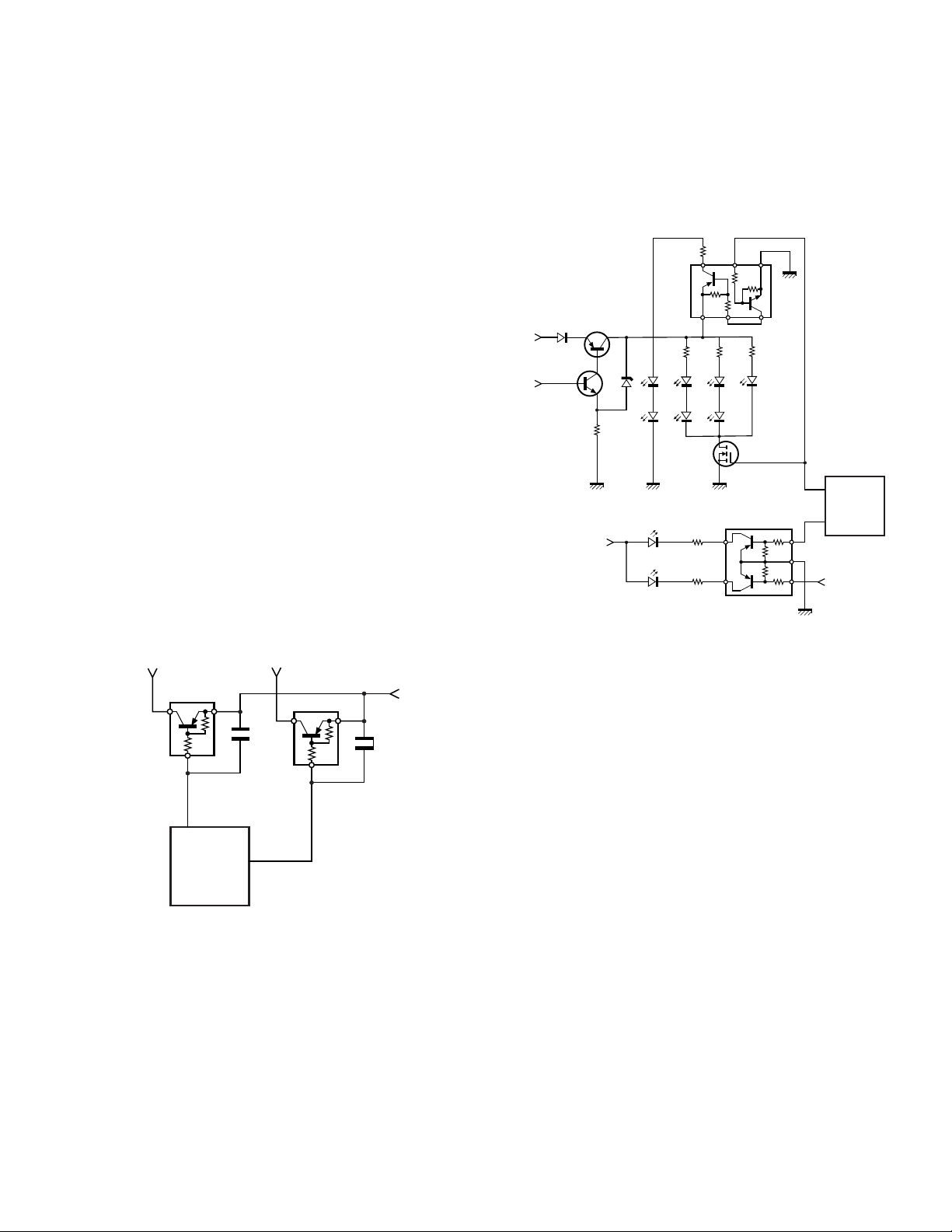
Power Supply Circuit
■ Charging Circuit
When an external power supply is connected to the DC IN
terminal, the constant-current circuit consisting of Q33 and
D31 provides a constant current of approx. 110 mA to the NiMH battery.
If no external power supply is connected to the DC IN
terminal, the constant-current circuit does not function.
IC8
MPU
BTEMP
DCDET
VR1
ENC
IC1
TCXO
Q4,5,6
D40,41
IC5
Q30
IC3,17
D9,14
Q16,17
Q22,23,24
Q59
Q9,10,13
D8,10
TH1
IC16
Q47
5MS
5MV
5C
5R
5T
Q41
RN2105
5MS SW
Q57
RN2105
5C SW
Q53
RN2701
5R SW
5MV SW
Q55
CPH3317
5T SW
5M
IC9
TK11250
CM
AVR
5.0V
IC12
TK11250
CUCB
AVR
5.0V
D35
RB521S-30
PROTECT
D36
RB521S-30
PROTECT
IC6
D48,49
D42,43,46
D47,44
AF AMP
Q36
2SJ347
THERM
DET
BTDET
Q35
2SK1830
DC-IN
DET
Q37, Q38
2SB1184
(Q,R)
2SC4617(R)
AF/LAMP
AVR
IC4
XC6202PB
52FR
AVR
11.5V
■ Power Supply Switching Circuit
The voltage supplied through the battery terminal or DC IN
terminal is branched in the power supply switching circuit as
shown in Fig.10 and then supplied to the required components.
■ Battery Type Recognition Circuit
When the battery pack is attached to the transceiver, the
battery type is recognized with the T terminal on the
transceiver. This battery type recognition activates charging
for the Ni-MH battery pack and displaying the battery meter.
-
T
+
BATT TERMINAL
7.5V Norminal
(6.0 - 9.0V)
Q33
2SB1184
(Q,R)
BATT
D31
DA221
CONSTANT
CURRENT
B
CHARGE
Q34
2SK1830
CHARGE
SW
D30
RB521S-30
PROTECT
CHARGE
D80
RB521S-30
PROTECT
D33
RB051L-40
PROTECT
B
D32
RB051L-40
PROTECT
DC IN
13.8V Norminal
(12.0 - 16.0V)
B
J2
Fig. 10 Charging and Power supply switching circuit
Control System
■ Reset and Backup Circuit
When power is supplied to the transceiver, the 5M voltage
goes “H” as C303 is charged.
A rising edge of the 5M voltage is detected by the voltage
detection IC (IC11) and when its output (RESET) goes “H”,
the reset status of the MPU is released.
5C
IC11
IN OUT
IC10
IN OUT INT
BATT
D35
IC9
IN OUT
5V
AVR
R244
C303
5M
+
If the supplied voltage to the transceiver is reduced and
the 5M voltage falls below the detection voltage of the voltage
detection IC (IC10), the MPU detects it by an interrupt
processing, backs up data in EEPROM (IC15) and turns the
power off.
Timing chart
Power
ON
5V5M
0
5VRESET
0
5VINT
Power
OFF
R243
C307
L63
IC15
EEPROM
IC8
MPU
RESET
10
0
Fig. 11 Reset and Backup circuit
Page 11
TH-K2AT/K2E/K2ET
CIRCUIT DESCRIPTION
■ Voltage Detection Circuit
Various voltages are input to the A/D port of the MPU (IC8)
for processing.
Battery voltage is divided with resistors (R240, R241) and
enters the BATT terminal (pin 52) of the MPU.
Battery voltage is used for battery meter indication during
transmission or for alert tone processing when an abnormal
power supply voltage (approx. 16.5 V or higher) is applied.
Squelch voltage becomes DC voltage by detecting changes
in noise voltage in the FM IC (IC3), and the signal is used for
squelch control.
The S meter voltage is output from the RSSI pin of the FM
IC to control S meter display.
Detection of thermistor voltage (temperature) in the Ni-MH
battery during charging, detection of remote microphone key
pressing and VOX voltage monitoring are performed through
each A/D port of the MPU.
■ Battery Save Circuit
If there is no signal (squelch off, scan off or no key operation)
for longer than 10 seconds, the transceiver will enter the
battery save mode.
Battery save operation is performed by controlling Q57 with
an output signal from the 5C (SAVE) terminal (pin 15) of the
MPU.
The 5C ON/OFF cycle ratio during battery saving can be set
from a transceiver menu.
■ LED Drive Circuit
The LCD and key illumination LEDs are lighted by controlling
Q51 for the LCD and Q50 for keys according to the output
voltage from the AF/LAMP AVR (Q37).
The BUSY and TX illumination LEDs are lighted by controlling
Q47.
Q47
D46
Q51
56
99
LAMP
RX LED
5T
AF AMP
D33
Q38
Q37
D48
D42
D42
D42
D44
D49
D43
D43
D43
D47
Q50
D41
BUSY LED
5C
TX LED
D40
R227
R226
B
Fig. 13 LED drive circuit
IC8
MPU
5MS
Q41
37
5MS
5C (SAVE)
IC8
MPU
5C
Q57
15
Fig. 12 Battery save circuit
5M
11
Page 12
TH-K2AT/K2E/K2ET
CIRCUIT DESCRIPTION
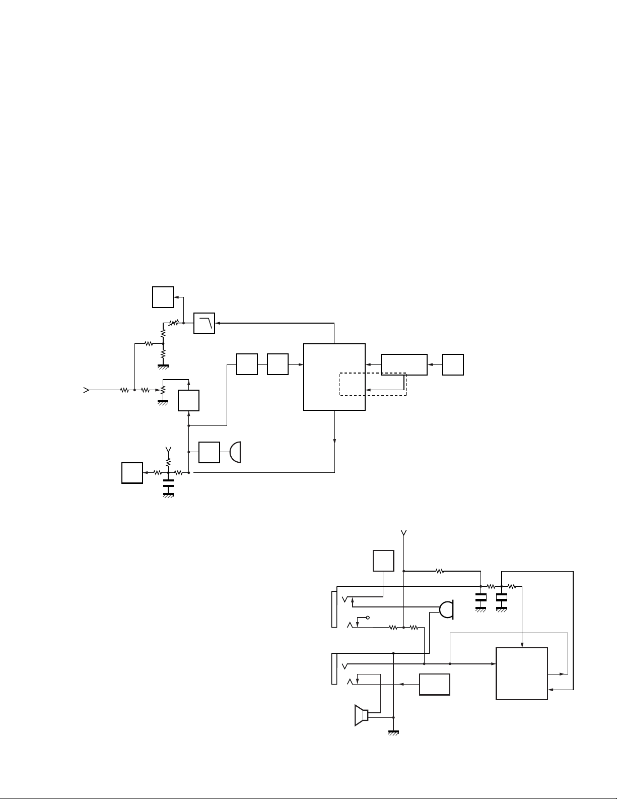
■ Key and Encoder Input Circuit
The POWER key is assigned to the interrupt port (pin 95) of
the MPU.
The PTT key is assigned to the dedicated port (pins 13, 14)
of the MPU.
16 key (K, K2, M, M2 and E3 types)
KIN1 KIN2 KIN3 KIN4
KIN0 KOUT0 KOUT1 KOUT2 KOUT3
MENU
F321
LAMP
VFO654
MONI
MR987
SET
CALL
∗
#0
Other keys composes a matrix and key presses are detected
by scanning them by software.
The encoder reads data using the interrupt port (pins 35
and 36) of the MPU.
IC8
MPU
PWRSW
SW
PTTI14PTTE13ENCB36ENCA
95
S7POWER
35
ROTARY
ENCODER
4 key (E type)
IC8
KIN0 KOUT0 KOUT1 KOUT2 KOUT3
KIN1 KIN2 KIN3 KIN4
MRVFOF
MENUCALL
LAMP
MONI
SET
MPU
Fig. 14 Key and Encoder input circuit
PWRSW
POWER
SW
J3
PTTI14PTTE13ENCB36ENCA
95
S7
J3
35
ROTARY
ENCODER
12
Page 13
TH-K2AT/K2E/K2ET
CIRCUIT DESCRIPTION
■ CTCSS/DCS
The encode signal is generated by the MPU (IC8) and output
from the TONE terminal (pin 41) of the MPU.
The unwanted high-frequency components of the encode
signal output from the MPU are removed with a low-pass filter,
and applied to VCO modulation input (MOD) and TCXO VC
terminal for modulation.
The VCO and TCXO modulation levels are adjusted by VR6
to produce flat modulation characteristics in low and high
ranges.
The decode signal is input to the SIGIN pin (pin 47) of the
MPU after the waveform of the audio signal from the FM IC is
rectified with a CTCSS/DCS filter (IC17). Then the set CTCSS
tone frequency and DCS code are detected by digital signal
processing in the MPU to control muting.
X1
TCXO
VC
VCO
VR6
MOD
VR5
1
MIC
AMP
6
LPF
AMP
IC16
50
■ DTMF
The DTMF signal is generated by the MPU (IC8) and is
output from the DTMF/BEEP terminal (pin 40) of the MPU.
The DTMF signal is mixed with an audio signal at the input
side of the AF amplifier (IC6), and is output as a monitor tone.
The DTMF signal is mixed with a modulation signal at the
input side of pre-emphasis in the microphone amplifier (IC16)
and used as a transmit signal.
■ VOX
The IC5 and Q30 amplify the audio signal captured in the
microphone, and then the signal is converted into the DC
Voltage D24 rectifies.
The DC voltage activates the MPU (IC8), and the VOX starts.
■ Weather Alert (K and K2 types only)
The IC17 apmlifies the detected signal from the FM IC (IC3),
and the MPU (IC8) processes the signal. This signal processing
activates Weather Alert function.
41
TONE
SIG INVOX IN
IC8
MPU
DTMF/BEEP
40
111
NOAA K, K2 types only
47
CTCSS/DCS
IC17D24Q30 IC3
9
FILTER
FM
IC
MIC
IC5
HPF
IC6
AF AMP
Vin
VOL OUT
Fig. 15 CTCSS/DCS, DTMF, VOX, Weather alert
■ Serial Control
Serial control must be enabled from a transceiver menu so
that the REM/TXD pin of the speaker jack (J4) and the PTT
(RXD) pin of the microphone jack (J3) function as TXD and
RXD, respectively, when communicating with a personal
computer.
MIC JACK
J3
J4
SP JACK
PTT
MIC
IM
REM/TXD
SP
5MS
SPG
SPK
AFO
IC5
HPF
5MC
10
+
–
POUT
IC6
AF AMP
MIC
46
REM
IC8
MPU
13
PTTE
TXD
RXD
12
11
Fig. 16 Serial control
13
Page 14

TH-K2AT/K2E/K2ET
SEMICONDUCTOR DATA
MPU : 90522BPFFG139 (IC8)
■ Pin function
Pin Pin
No. Name
1 CLOCK O Common serial clock output
2 DATA O Common serial data output
3 EEPDI I Data input from EEPROM
4 EEPCS O Chip select output to EEPROM
5 VOX O VOX power supply switch L:ON
BPF/APC
6
7 KAPC O APC ON/OFF switch L:APC ON
8 VCC - Positive power supply
9 AFM O AF mute switch L:Mute
10 SPM O Speaker mute switch H:Mute
11 RXD I UART data input line from PC (9600bps)
12 TXD O UART data output line to PC (9600bps)
13 PTTE I External [PTT] key input L:ON
14 PTTI I [PTT] key input L:ON
15
5C(SAVE)
16 FINAL O
17 SEG0 O LCD segment output 0
18 SEG1 O LCD segment output 1
19 SEG2 O LCD segment output 2
20 SEG3 O LCD segment output 3
21 SEG4 O LCD segment output 4
22 SEG5 O LCD segment output 5
23 SEG6 O LCD segment output 6
24 SEG7 O LCD segment output 7
25 SEG8 O LCD segment output 8
26 SEG9 O LCD segment output 9
27 SEG10 O LCD segment output 10
28 SEG11 O LCD segment output 11
29 SEG12 O LCD segment output 12
30 SEG13 O LCD segment output 13
31 SEG14 O LCD segment output 14
32 SEG15 O LCD segment output 15
33 VSS - GND
34 COR1
35 ENCA I Encoder A side input
36 ENCB I Encoder B side input
37 5MS O 5MS main power supply switch L:ON
38 DVCC - Reference voltage input for DAC
39 DVSS - Ground for DAC
DTMF/
40
BEEP 1750Hz (D/A)
41 TONE O
42 AVCC - Positive power supply for ADC
43 AVRH - Reference voltage input for ADC
44 AVRL - Ground reference voltage input for ADC
45 AVSS - Ground for ADC
46 REM I
47 SIGIN I
14
I/O Function
BPF tuning voltage output, APC voltage
O
output (PWM)
O Save power supply switch L:ON
Gate bias control of TX final amplifier
L:Bias ON
- Power supply stabilization (Connected to
VSS through 0.1uF)
Encode waveform output of DTME/BEEP/
O
Encode waveform output of CTCSS/DCS
(D/A)
Remote control microphone key voltage
input (A/D)
Decode waveform input of CTCSS/DCS
(A/D)
Pin Pin
No. Name
48 SQ I Noise voltage input for squelch (A/D)
49 SM I RSSI voltage input for S-meter (A/D)
50 VOXIN I Microphone voltage input for VOX (A/D)
51 THERM I TX temperature compensation input(A/D)
52 BATT I Battery voltage input (A/D)
53 BTEMP I
54 VCC - Positive power supply
55
CHARGE
56 LAMP O Lamp power supply switch H:ON
57 AFAMP O
58 NAR O Wide/Narrow switching H:Narrow
59 COM0 O LCD common output 0
60 COM1 O LCD common output 1
61 COM2 O LCD common output 2
62 COM3 O LCD common output 3
63 VSS - GND
64 SEG16 O LCD segment output 16
65 SEG17 O LCD segment output 17
66 SEG18 O LCD segment output 18
67 SEG19 O LCD segment output 19
68 SEG20 O LCD segment output 20
69 SEG21 O LCD segment output 21
70 SEG22 O LCD segment output 22
71 SEG23 O LCD segment output 23
72 SEG24 O LCD segment output 24
73 NC - Not used
74 NC - Not used
75 SEG25 O LCD segment output 25
76 SEG26 O LCD segment output 26
77 SEG27 O LCD segment output 27
78 SEG28 O LCD segment output 28
79 SEG29 O LCD segment output 29
80 SEG30 O LCD segment output 30
81 SEG31 O LCD segment output 31
82 V0 - Not used
83 V1 - Not used
84 V2 - Not used
85 V3 - LCD drive power supply 3
86
HST(VCC)
87 MD2 I L fixed
88 MD1 I H fixed
89 MD0 I H fixed
90 RESET I Reset input L:Reset
91 VSS - GND
92 X0 I System clock (7.9872MHz)
93 X1 O System clock (7.9872MHz)
94 VCC - Positive power supply
95 PWRSW I Power switch interrupt input (↓)
96 INTUP I Power supply voltage interrupt input (↑)
97 INTDW I Power supply voltage interrupt input (↓)
I/O Function
Detection of thermistor voltage (temperature)
in the Ni-MH battety (A/D)
Battery charge circuit power supply switch
O
AF amplifier/Lamp AVR power supply
switch H:ON
I Not used (VCC)
H:ON
Page 15

TH-K2AT/K2E/K2ET
SEMICONDUCTOR DATA / COMPONENTS DESCRIPTION
Pin Pin
No. Name
98 DCDET I
99 RXLED O Busy LED output H:ON
100 BSFT O Beat shift swiching output H:ON
101 PLLEN O Serial enable output to PLL IC
102 PLLLD I
103 KIN0 I Key matrix input 0
104 KIN1 I Key matrix input 1
105 KIN2 I Key matrix input 2
106 KIN3 I Key matrix input 3
107 KIN4 I Key matrix input 4
108 TYPE I Market code bit input
109 VUKEY I Detection of 4 key or 16 key
110 MICM O Microphone mute switch H:Mute
111 NOAA I 1050Hz tone detection input
112 5R O RX power supply switch L:ON
113 SHIFT O VCO shift switch L:TX, H:RX
114 5T O TX power supply switch L:ON
115 KOUT0 O Key matrix output 0
116 KOUT1 O Key matrix output 1
117 KOUT2 O Key matrix output 2
118 KOUT3 O Key matrix output 3
119 VSS - GND
120 BTDET O Battery detection switch L:ON
I/O Function
DC IN detection interrupt input (↓)
L:DC IN connected
Lock detection input from PLL IC H: Lock
COMPONENTS DESCRIPTION
TX-RX UNIT (X57-674X-XX)
Ref. No.
IC10
IC11
IC12 5.0V AVR
IC15 EEPROM
IC16
IC17
Q5,6,9 RF amplifier
Q10,11
Q12
Q13
Q14
Q15
Q16 1st mixer
Q17
Q20
Q21 Audio filter Active filter
Q22
Q23 Tripler 2nd local
Q24 IF amplifier 1st IF 38.85MHz
Q27
Q29
Q30
Q31
Q33
Use/Function
IC1 PLL IC
APC differential
IC2
amplifier
IC3 FM IC
IC4 11.5V AVR
IC5 HPF Active filter
IC6 AF amplifier
IC8 MPU
IC9 5.0V AVR
4.4V voltage
detection
3.3V voltage
detection
MIC amplifier
CTCSS/DCS/WX
filter
Q1 VCO
Q2 RF amplifier
VCO shift
Q3
control switch
Q4 Ripple filter
Drive amplifier
Power amplifier
APC circuit
operation switch
APC output
switch
Q10 operation
switch
RX 1st amplifier
Audio mute
switch
Wide/narrow
changeover switch
Wide/narrow
changeover switch
MIC mute
switch
VOX detection
amplifier
Q56 operation
switch
Charge switch
Operation/Condition/Compatibility
MPU INT voltage detection
MPU Reset voltage detection
Limiter, splatter filter
Active filter
On RX
On TX
On TX
On TX
Audio mute when off
On when wide is selected
On when wide is selected
Mutes when ON
Off when the speaker outputs audio
15
Page 16

TH-K2AT/K2E/K2ET
COMPONENTS DESCRIPTION
Ref. No.
Q34
Q35
Q36
Q37
Q38
Q41 5MS switch On when 5MS is applied
Q47
Q50
Q51
Q52
Q53
Q55 5T switch On when 5T is applied
Q56
Q57 5C switch On when 5C is applied
Q58
Q59
D1,2
D10-13
D14
D15
D16
D17
D18-21
D22
D24
D25
D26
D27
D30
D31
D32
Use/Function
Q33 operation
switch
DC IN detection
Ni-MH temperature
detection
AF amplifier/
Lamp AVR
Q37 operation
switch
TX/BUSY LED
switch
Key LED switch
LCD LED switch
Beat shift switch
5R/5MV switch
Speaker mute
switch
Q12 gate
voltage switch
WX detection
amplifier
VCO frequency
control
D5
Frequency shift
D6
VCO modulation
D7 Speed up Ripple filter
D8 RF switch On TX
D9 RF switch On RX
Antenna switch
Reverse current
prevention
APC output
voltage limiter
PLL lock detection
Over input
protection
RX BPF tuning
MIC mute control
VOX detection
rectification
Speaker mute
speed up
C246 discharge
MIC ALC
rectification
Reverse current
prevention
Constant-current
circuit
Reverse current
prevention
Operation/Condition/Compatibility Ref. No.
On when charging
H: DC IN detection
On when temperature detection is
activated
On when the speaker outputs audio or
lamp lights
On when the key LED lights
On when the LCD LED lights
On when 5R or 5MV is applied
Off when High power is selected
On TX
APC reference voltage
Charge current
Constant-current charge
DC IN
Use/Function
Reverse current
D33
prevention
AVR
D34
constant-voltage
Reverse current
D35
prevention
Reverse current
D36
prevention
D40 TX LED Lights on TX
D41 BUSY LED Lights on RX
D42-44
D46,47
D48,49
D62-65
D69-72
D74,79 Limiter
Key illumination
LED
LCD illumination
LED
Key type
D60
detection
market code
detection
Reverse current
prevention
D73 Voltage drop
Reverse current
D80
prevention
Operation/Condition/Compatibility
Battery
Battery
DC IN
Key backlight illumination
LCD backlight illumination
Key matrix
16
Page 17

PARTS LIST
New Parts. indicates safety critical components.
∗
Parts without Parts No. are not supplied.
Les articles non mentionnes dans le Parts No. ne sont pas fournis.
Teile ohne Parts No. werden nicht geliefert.
TH-K2AT/K2E/K2ET (Y50-580X-XX)
TX-RX UNIT (X57-674X-XX)
Ref. No.
1 3A,2G * A02-3817-02 CABINET ASSY(BATTERY CASE) K2,M2
21C*A02-3818-23 CABINET ASSY(4KEY) E
31A*A02-3819-23 CABINET ASSY(16KEY) K,K2,M
31A*A02-3819-23 CABINET ASSY(16KEY) M2,E3
4 3A,3C * A10-4066-11 CHASSIS
5 3B,3D * A82-0053-02 REAR PANEL
6 1B,1D * B09-0675-03 CAP(SP/MIC/DC IN)
7 1A,1C * B10-2746-03 FRONT GLASS
8 1B,1D * B11-1805-03 ILLUMINATION GUIDE(LCD)
9 2B,2D * B11-1806-04 FILTER(LCD)
10 1B,1D * B38-0881-05 LCD
11 1G * B62-1695-00 INSTRUCTION MANUAL(CHINESE) M2
11 1E,1G * B62-1696-00 INSTRUCTION MANUAL(ENGLISH)
11 1E,1G * B62-1697-00 INSTRUCTION MANUAL(SPANISH) K,K2,E
11 1E * B62-1697-00 INSTRUCTION MANUAL(SPANISH) E3
11 1E * B62-1699-00 INSTRUCTION MANUAL(GERMAN) E,E3
11 1E * B62-1702-00 INSTRUCTION MANUAL(ITALIAN) E,E3
11 1E * B62-1757-00 INSTRUCTION MANUAL(FRENCH) E,E3
11 1E * B62-1758-00 INSTRUCTION MANUAL(DUTCH) E,E3
12 3A * B72-2128-04 MODEL NAME PLATE(TH-K2AT) K,K2,M
12 3A * B72-2128-04 MODEL NAME PLATE(TH-K2AT) M2
12 3C * B72-2129-04 MODEL NAME PLATE(TH-K2E) E
12 3A * B72-2193-04 MODEL NAME PLATE(TH-K2ET) E3
13 2B,2D * E04-0443-05 RF COAXIAL RECEPTACLE(SMA)
14 2A,2C * E23-1234-04 TERMINAL(BATTERY)
15 2B,2D * E29-1199-04 INTER CONNECTOR(LCD)
16 1A,1C * E37-1106-05 LEAD WIRE WITH CONNECTOR(SP)
17 2A,2C * F10-2464-04 SHIELDING COVER(FINAL FET)
18 2A,2C * F10-2465-04 SHIELDING COVER(ANT TERMINAL)
19 2B,2D * F15-1008-04 SHADOW PLATE(LCD)
-*G10-1317-04 FIBROUS SHEET(SP NET)
21 3B,3D G53-1529-04 PACKING(VOL/ENC)
22 2A,2C * G53-1572-02 PACKING(CASE)
23 2B,2D * G53-1589-03 PACKING(SP/MIC)
24 3E * H52-1960-02 ITEM CARTON CASE(TH-K2AT) K,M
24 3E * H52-1961-02 ITEM CARTON CASE(TH-K2E) E
24 3E * H52-1962-02 ITEM CARTON CASE(TH-K2ET) E3
25 2H * H52-2009-02 ITEM CARTON CASE(TH-K2AT) K2,M2
26 2F * H12-3146-01 PACKING FIXTURE K,M,E
26 2F * H12-3146-01 PACKING FIXTURE E3
27 3G * H12-3147-03 PACKING FIXTURE K2,M2
28 2A,2C * J19-5451-03 HOLDER(TERMINAL)
29 1B,1D * J21-8456-03 HARDWARE FIXTURE(LCD)
30 2E,3G * J29-0709-04 BELT HOOK ASSY ACCESSORY
31 2A,2C * J30-1284-04 SPACER(PTT KNOB)
32 3E,2G J69-0342-05 HANDSTRAP ACCESSORY M,M2,E
32 3E J69-0342-05 HANDSTRAP ACCESSORY E3
33 2B,2D J82-0076-05 FPC(VOL/ENC)
45 3A,3C J99-0376-04 ADHESIVE TAPE
34 1B,1D K29-5150-03 KNOB(VOL)
35 1B,1D K29-5159-03 KNOB(ENC)
E : TH-K2E K : TH-K2AT M : TH-K2AT
E3 : TH-K2ET K2 : TH-K2AT M2 : TH-K2AT
Address
New
Parts No. Description
parts
TH-K2AT/K2E/K2ET
Destination Destination
TH-K2AT/K2E/K2ET
L:
Scandinavia
Y:
PX (Far East, Hawaii)
Y:
AAFES (Europe)
Ref. No.
36 1A * K29-9272-02 KEY TOP(16KEY) K,K2,M
36 1A * K29-9272-02 KEY TOP(16KEY) M2,E3
37 1A,1C * K29-9274-03 KNOB(PTT/LAMP/MONI)
38 1C * K29-9276-02 KEY TOP(4KEY) E
A 2B,2D N09-1492-05 PAN HEAD SCREW(SMA)
B 1B,1D N14-0569-04 CIRCULAR NUT(VOL/ENC)
C 1B,1D N14-0573-04 CIRCULAR NUT(SMA)
D 1A,1C N79-2035-46 PAN HEAD TAPTITE SCREW(PCB)
E 2A,2C N79-2040-45
F 3A,3C N82-2007-46 PAN HEAD TAPTITE SCREW(CASE)
G 2A,2C N09-2433-05
39 2B,2D R39-0602-05 VARIABLE RESISTOR
40 1A,1C T07-0341-15 SPEAKER
41 2F,3G * T90-1018-25 HELICAL ANTENNA ACCESSORY
42 2F * W08-0959-15 CHARGER(230V/13.8V) ACCESSORY M,E,E3
43 2E * W08-0960-15 CHARGER(120V/13.8V) ACCESSORY K
44 2E * W09-0991-05
44 2E * W09-0991-05
Address
0-11 : K, K2 0-21 : M, M2 2-71 : E 2-72 : E3
D40 B30-2156-05 LED(RED)
D41 B30-2157-05 LED(YELLOW)
D42-44 B30-2205-05 LED(YG) E3
D42-44 B30-2205-05 LED(YG) K,K2,M
D42-44 B30-2205-05 LED(YG) M2
D42,43 B30-2205-05 LED(YG) E
D46 B30-2205-05 LED(YG) E
D46,47 B30-2205-05 LED(YG) E3
D46,47 B30-2205-05 LED(YG) K,K2,M
D46,47 B30-2205-05 LED(YG) M2
D48,49 B30-2237-05 LED(YG)
C1 CK73HB1C103K CHIP C 0.010UF K
C2 CK73HB1H102K CHIP C 1000PF K
C3 CC73GCH1H030B CHIP C 3.0PF B
C4 CK73HB1H102K CHIP C 1000PF K
C5 CK73HB1A104K CHIP C 0.10UF K
C6 CK73HB1H102K CHIP C 1000PF K
C7 CC73HCH1H0R5B CHIP C 0.5PF B
C8,9 CC73GCH1H270G CHIP C 27PF G
C10 CK73HB1C103K CHIP C 0.010UF K
C11 CK73HB1H102K CHIP C 1000PF K
C13 CC73GCH1H0R5B CHIP C 0.5PF B
C14 CK73HB1H102K CHIP C 1000PF K
C15 CC73HCH1H120J CHIP C 12PF J
C17,18 CK73HB1H102K CHIP C 1000PF K
C19 CC73HCH1H150J CHIP C 15PF J
C20 CC73HCH1H080D CHIP C 8.0PF D
C21 CK73HB1H102K CHIP C 1000PF K
C22 CC73HCH1H180J CHIP C 18PF J
C24-26 CK73HB1H102K CHIP C 1000PF K
C27 C92-0628-05 CHIP-TAN 10UF 10WV
C30 CK73HB1H102K CHIP C 1000PF K
K:
New
parts
USA
T:
England
X:
Australia
P:
Canada
E:
Europe
M:
Other Areas
Parts No. Description
PAN HEAD TAPTITE SCREW(HOLDER,R PANEL)
PAN HEAD TAPTITE SCREW(FINAL FET)
BATTERY ASSY(7.2V/1100MAH) ACCESSORY
BATTERY ASSY(7.2V/1100MAH) ACCESSORY
TX-RX UNIT (X54-674X-XX)
K,M,E
E3
17
Page 18

TH-K2AT/K2E/K2ET
PARTS LIST
TX-RX UNIT (X57-674X-XX)
New
Ref. No.
C33 C92-0002-05 CHIP-TAN 0.22UF 35WV
C34 C92-0714-05 TANTALUM 4.7UF 6.3WV
C35 C92-0001-05 CHIP-C 0.1UF 35WV
C37 CK73HB1H102K CHIP C 1000PF K
C38 CK73HB1C103K CHIP C 0.010UF K
Address
Parts No. Description
parts
Destination
New
Ref. No.
C136 CC73HCH1H100D CHIP C 10PF D
C137 CC73HCH1H050C CHIP C 5.0PF C
C138 CK73HB1H102K CHIP C 1000PF K
C141,142 CK73HB1H102K CHIP C 1000PF K
C145 CC73HCH1H220G CHIP C 22PF G
Address
Parts No. Description
parts
Destination
C40 CK73HB1A104K CHIP C 0.10UF K
C41 C92-0507-05 CHIP-TAN 4.7UF 6.3WV
C42 CK73HB1H102K CHIP C 1000PF K
C43 CK73HB1C103K CHIP C 0.010UF K
C44-46 CC73HCH1H101J CHIP C 100PF J
C50 CC73HCH1H220J CHIP C 22PF J
C51 CC73GCH1H220J CHIP C 22PF J
C52 CC73HCH1H100D CHIP C 10PF D
C54 CK73HB1H102K CHIP C 1000PF K
C55 CK73HB1C103K CHIP C 0.010UF K
C56 CK73HB1H102K CHIP C 1000PF K
C57 CC73HCH1H100D CHIP C 10PF D
C61 CK73HB1H102K CHIP C 1000PF K
C64 CK73HB1H102K CHIP C 1000PF K
C65 CC73HCH1H180J CHIP C 18PF J
C66 CK73GB0J105K CHIP C 1.0UF K
C67 CK73HB1H102K CHIP C 1000PF K
C68 CC73HCH1H180J CHIP C 18PF J
C69 CC73HCH1H040C CHIP C 4.0PF C
C70 CK73GB0J105K CHIP C 1.0UF K
C71 CK73HB1H102K CHIP C 1000PF K
C72 CK73GB1C104K CHIP C 0.10UF K
C73 CK73HB1H102K CHIP C 1000PF K
C74 CC73HCH1H330J CHIP C 33PF J
C75 CK73HB1H102K CHIP C 1000PF K
C76 CC73GCH1H390J CHIP C 39PF J
C78 CK73HB1H102K CHIP C 1000PF K
C82 CK73HB1H102K CHIP C 1000PF K
C83 CK73HB1C103K CHIP C 0.010UF K
C84 CK73HB1A104K CHIP C 0.10UF K
C147 CK73HB1H102K CHIP C 1000PF K
C148 CC73HCH1H220G CHIP C 22PF G
C152,153 CK73HB1H102K CHIP C 1000PF K
C158 CC73HCH1H220G CHIP C 22PF G
C159 CC73HCH1H020B CHIP C 2.0PF B
C160 CC73HCH1H270G CHIP C 27PF G
C161 CK73HB1H102K CHIP C 1000PF K
C162 ∗ CC73HCH1H470G CHIP C 47PF G
C163 CK73HB1H102K CHIP C 1000PF K
C166 CK73HB1C103K CHIP C 0.010UF K
C167,168 CK73HB1A104K CHIP C 0.10UF K
C169,170 CK73HB1A683K CHIP C 0.068UF K
C171 CK73HB1H102K CHIP C 1000PF K
C172 CK73HB1H182K CHIP C 1800PF K
C173,174 ∗ CC73HCH1H181J CHIP C 180PF J
C175 CC73HCH1H220J CHIP C 22PF J
C176 CK73HB1A104K CHIP C 0.10UF K
C177 C92-0712-05 CHIP-TAN 22UF 6.3WV
C178 CK73HB1C103K CHIP C 0.010UF K
C179 CK73HB1A104K CHIP C 0.10UF K
C180 CC73HCH1H121J CHIP C 120PF J
C182,183 CK73HB1A104K CHIP C 0.10UF K
C186 CC73HCH1H240J CHIP C 24PF J
C187 CC73HCH1H020C CHIP C 2.0PF C
C188 CC73HCH1H240J CHIP C 24PF J
C189 CK73HB1H102K CHIP C 1000PF K
C190-192 CK73HB1C103K CHIP C 0.010UF K
C193 C92-0507-05 CHIP-TAN 4.7UF 6.3WV
C194 CK73HB1A104K CHIP C 0.10UF K
C195 C92-0628-05 CHIP-TAN 10UF 10WV
C85 ∗ C93-0766-05 CERAMIC C 56PF J
C88 CC73GCH1H560J CHIP C 56PF J
C89 CK73GB1H102K CHIP C 1000PF K
C90-92 CK73HB1H102K CHIP C 1000PF K
C93 CC73HCH1H080D CHIP C 8.0PF D
C94 CK73GB1H102K CHIP C 1000PF K
C95-97 CC73GCH1H120G CHIP C 12PF G
C98 CC73GCH1H080B CHIP C 8.0PF B
C99 CC73GCH1H130G CHIP C 13PF G
C100 CC73GCH1H070B CHIP C 7.0PF B
C101 CC73GCH1H240G CHIP C 24PF G
C105-107 CK73HB1H102K CHIP C 1000PF K
C108 CC73HCH1H101J CHIP C 100PF J
C109-115 CK73HB1H102K CHIP C 1000PF K
C116 C92-0544-05 CHIP-TAN 10UF 4WV
C117,118 CK73HB1H102K CHIP C 1000PF K
C124 CK73HF1C104Z CERAMIC C 0.1UF Z
C125 CC73HCH1H1R5C CHIP C 1.5PF C
C126 CC73HCH1H100D CHIP C 10PF D
C128 CK73HB1C103K CHIP C 0.010UF K
C129 CC73HCH1H110J CHIP C 11PF J
C130 CK73HB1H102K CHIP C 1000PF K
C131-133 CK73HB1C103K CHIP C 0.010UF K
C134 CK73HB1H102K CHIP C 1000PF K
C135 CC73HCH1H120J CHIP C 12PF J
E : TH-K2E K : TH-K2AT M : TH-K2AT
18
E3 : TH-K2ET K2 : TH-K2AT M2 : TH-K2AT
C196,197 CK73HB1C682K CHIP C 6800PF K
C198 CK73EF1C105Z CHIP C 1.0UF Z
C201 CK73HB1H122K CHIP C 1200PF K
C202 CK73HB1H271K CHIP C 270PF K
C203 CC73HCH1H121J CHIP C 120PF J
C204 CK73HB1A333K CHIP C 0.033UF K
C205 CK73HB1A473K CHIP C 0.047UF K
C206 CK73HB1C153K CHIP C 0.015UF K
C207 CK73HB1C103K CHIP C 0.010UF K
C208 CC73HCH1H820J CHIP C 82PF J
C209 CK73HB1H102K CHIP C 1000PF K
C210 CK73HB1C103K CHIP C 0.010UF K
C211 CK73HB1H222K CHIP C 2200PF K
C212 CK73HB1C123K CHIP C 0.012UF K
C213 C92-0507-05 CHIP-TAN 4.7UF 6.3WV
C218 CK73HB1H102K CHIP C 1000PF K
C219 CK73HB1A473K CHIP C 0.047UF K
C220 CK73HB1E472K CHIP C 4700PF K
C221,222 CK73HB1C103K CHIP C 0.010UF K
C223 CK73HB1H102K CHIP C 1000PF K
C224 CK73HB1A104K CHIP C 0.10UF K
C225 CK73GB0J105K CHIP C 1.0UF K
C226 CK73HB1A104K CHIP C 0.10UF K
C227 C92-0587-05 CHIP-TAN 2.2UF 4WV
C228,229 CK73HB1A104K CHIP C 0.10UF K
Page 19

New
Ref. No.
C230 CK73FB1C105K CHIP C 1.0UF K
C231,232 CK73HB1H102K CHIP C 1000PF K
C235,236 CK73HB1C103K CHIP C 0.010UF K
C237 C92-0628-05 CHIP-TAN 10UF 10WV
C238-241 CK73HB1H102K CHIP C 1000PF K
Address
Parts No. Description
parts
TH-K2AT/K2E/K2ET
PARTS LIST
Destination
Ref. No.
C359,360 CK73HB1A104K CHIP C 0.10UF K
C366 ∗ CC73GCH1H101G CHIP C 100PF G
C500,501 CC73HCH1H1R5B CHIP C 1.5PF B
C502 CC73HCH1H030B CHIP C 3.0PF B
C503 ∗ CC73GCH1H101G CHIP C 100PF G
Address
New
Parts No. Description
parts
TX-RX UNIT (X57-674X-XX)
Destination
C242 CK73HB1C103K CHIP C 0.010UF K
C243 CK73HB1H102K CHIP C 1000PF K
C246 C92-1327-05 CHIP-TAN 100UF 10WV
C247,248 CK73HB1A104K CHIP C 0.10UF K
C249 CK73HB1H102K CHIP C 1000PF K
C250 CK73EF1C105Z CHIP C 1.0UF Z
C252 CC73HCH1H101J CHIP C 100PF J
C253 C92-0628-05 CHIP-TAN 10UF 10WV
C255 C92-0628-05 CHIP-TAN 10UF 10WV
C256,257 CK73HB1H102K CHIP C 1000PF K
C258 CK73HB1A104K CHIP C 0.10UF K
C270,271 CK73HB1H102K CHIP C 1000PF K
C272 CK73HB1H471K CHIP C 470PF K
C276 CK73HB1H102K CHIP C 1000PF K
C279-285 CK73HB1H102K CHIP C 1000PF K
C286 CK73FB1C105K CHIP C 1.0UF K
C290,291 CK73HB1H102K CHIP C 1000PF K
C293 CC73HCH1H470J CHIP C 47PF J
C294,295 CC73HCH1H050C CHIP C 5.0PF C
C297 CK73HB1A104K CHIP C 0.10UF K
C298 CK73HB1H102K CHIP C 1000PF K
C299 CK73FB1C105K CHIP C 1.0UF K
C300 CK73HB1H102K CHIP C 1000PF K
C302 CK73HB1H102K CHIP C 1000PF K
C303 C92-0605-05 TANTALUM C150UF 6.3WV
C304-306 CK73HB1H102K CHIP C 1000PF K
C307 CK73HB1A104K CHIP C 0.10UF K
C308 CK73HB1H102K CHIP C 1000PF K
C309 CK73FB1C105K CHIP C 1.0UF K
C310 CK73EF1C105Z CHIP C 1.0UF Z
C311 CK73GB1C104K CHIP C 0.10UF K
C312,313 CK73HB1A393K CHIP C 0.039UF K
C314 CK73HB1H102K CHIP C 1000PF K
C316 CK73GB1C104K CHIP C 0.10UF K
C317,318 CK73HB1H102K CHIP C 1000PF K
C319 C92-0628-05 CHIP-TAN 10UF 10WV
C320,321 CK73HB1C822K CHIP C 8200PF K K,K2
C323-326 CK73HB1H102K CHIP C 1000PF K
C327 CK73HB1A104K CHIP C 0.10UF K
C328 CK73GB0J105K CHIP C 1.0UF K
C329 CC73FCH1H560J CHIP C 56PF J
C330,331 CK73HB1H102K CHIP C 1000PF K
C332 CK73HB1A104K CHIP C 0.10UF K
C335,336 CK73HB1A104K CHIP C 0.10UF K
C338 CK73FB1C105K CHIP C 1.0UF K
C339 CK73HB1A473K CHIP C 0.047UF K
C344-348 CK73HB1H102K CHIP C 1000PF K
C349 CK73HB1A104K CHIP C 0.10UF K M,M2,E
C349 CK73HB1A104K CHIP C 0.10UF K E3
C349,350 CK73HB1A104K CHIP C 0.10UF K K,K2
C351 CK73HB1C103K CHIP C 0.010UF K
C352-354 CK73HB1H102K CHIP C 1000PF K
C355,356 CK73HB1C103K CHIP C 0.010UF K
C357 CK73EF1C105Z CHIP C 1.0UF Z
C358 CK73HB1A473K CHIP C 0.047UF K
E : TH-K2E K : TH-K2AT M : TH-K2AT
E3 : TH-K2ET K2 : TH-K2AT M2 : TH-K2AT
C504 CC73HCH1H020B CHIP C 2.0PF B
C505 CK73HB1A473K CHIP C 0.047UF K
C506 CK73HB1H102K CHIP C 1000PF K
C510 CC73HCH1H101J CHIP C 100PF J E,E3
C511,512 CK73HB1H471K CHIP C 470PF K E,E3
C514 CK73GB1H471K CHIP C 470PF K E,E3
C515-517 CK73HB1H471K CHIP C 470PF K E,E3
CN1 E40-5915-05 FLAT CABLE CONNECTOR
CN2 E40-5929-05 PIN ASSY
CN6 ∗ E40-6327-05 PIN ASSY
CN7 E40-5630-05 PIN ASSY SOCKET
CN8 ∗ E40-6308-05 PIN ASSY
CN9 ∗ E40-6309-05 PIN ASSY SOCKET
CN15 E23-1081-05 TERMINAL
CN17 E23-1081-05 TERMINAL E,E3
J2 E03-0190-05 DC JACK
J3 ∗ E11-0484-05 3.5D PHONE JACK(3.5D)
J4 ∗ E11-0483-05 2.5D PHONE JACK(2.5D)
CN10 ∗ F01-1032-05 RADIATION PLATE
F1 ∗ F53-0286-05 FUSE(2.5A/32V)
F3 ∗ F53-0287-05 FUSE(0.5A/32V)
CD1 L79-1474-05 TUNING COIL
CF1 L72-0968-05 CERAMIC FILTER
L1 L40-1001-86 SMALL FIXED INDUCTOR(10UH)
L2 L41-4778-14 SMALL FIXED INDUCTOR
L3 L41-8278-14 SMALL FIXED INDUCTOR
L5,6 L40-1001-86 SMALL FIXED INDUCTOR(10UH)
L8 ∗ L40-1285-71 SMALL FIXED INDUCTOR(120NH)
L9-11 ∗ L40-8275-71 SMALL FIXED INDUCTOR(82NH)
L12 L40-1075-71 SMALL FIXED INDUCTOR(10NH)
L13 L92-0149-05 FERRITE CHIP
L14 ∗ L41-4778-14 SMALL FIXED INDUCTOR
L15 L41-6868-14 SMALL FIXED INDUCTOR
L16 L34-4577-05 AIR-CORE COIL
L17 L34-4606-05 AIR-CORE COIL
L18 ∗ L41-2285-14 SMALL FIXED INDUCTOR
L19 L34-4569-05 AIR-CORE COIL
L20 L34-4567-05 AIR-CORE COIL
L21-23 L34-4569-05 AIR-CORE COIL
L26 ∗ L41-4785-14 SMALL FIXED INDUCTOR
L27 ∗ L41-6885-14 SMALL FIXED INDUCTOR
L28 L40-2775-71 SMALL FIXED INDUCTOR(27NH)
L29 L40-2275-71 SMALL FIXED INDUCTOR(22NH)
L32 L41-8278-14 SMALL FIXED INDUCTOR
L35 L41-8278-14 SMALL FIXED INDUCTOR
L38 L41-8278-14 SMALL FIXED INDUCTOR
L40 L41-6878-14 SMALL FIXED INDUCTOR
L41 L41-1878-14 SMALL FIXED INDUCTOR
L45,46 ∗ L41-5685-14 SMALL FIXED INDUCTOR
L49 L92-0131-05 FERRITE CHIP
L50 L92-0137-05 FERRITE CHIP
L53 L40-1575-71 SMALL FIXED INDUCTOR(15NH)
L54 ∗ L40-5675-71 SMALL FIXED INDUCTOR(56NH)
19
Page 20

TH-K2AT/K2E/K2ET
PARTS LIST
TX-RX UNIT (X57-674X-XX)
New
Ref. No.
L55 L41-1078-14 SMALL FIXED INDUCTOR
L56 ∗ L41-2278-14 SMALL FIXED INDUCTOR
L58 ∗ L41-8285-14 SMALL FIXED INDUCTOR
L63 L92-0140-05 FERRITE CHIP
L64 L40-4795-85 SMALL FIXED INDUCTOR(4.7UH)
Address
Parts No. Description
parts
Destination
New
Ref. No.
R70-72 RK73EB2ER39K CHIP R 0.39 K 1/4W
R74,75 RK73HH1J104D RESISTOR 100K D 1/16W
R76-79 RK73HH1J154D RESISTOR 150K D 1/16W
R80 RK73HB1J103J CHIP R 10K J 1/16W
R81 RK73HB1J394J CHIP R 390K J 1/16W
Address
Parts No. Description
parts
Destination
L66 ∗ L40-1285-71 SMALL FIXED INDUCTOR(120NH)
L68 L92-0161-05 BEADS CORE
X1 ∗ L77-1931-05 TCXO(12.8MHZ)
X3 ∗ L77-1940-05 CRYSTAL RESONATOR(7.982MHZ)
XF1 ∗ L71-0619-05 MCF(38.85MHZ)
CP1 ∗ RK75HA1J272J CHIP-COM 2.7K J 1/16W
CP2 RK75GB1J392J CHIP-COM 3.9K J 1/16W
CP31 RK75GB1J392J CHIP-COM 3.9K J 1/16W
CP32-35 RK75HA1J102J CHIP-COM 1.0K J 1/16W
R4 RK73HB1J102J CHIP R 1.0K J 1/16W
R5 RK73HB1J104J CHIP R 100K J 1/16W
R6 RK73HB1J102J CHIP R 1.0K J 1/16W
R7 RK73HB1J473J CHIP R 47K J 1/16W
R8 RK73HB1J104J CHIP R 100K J 1/16W
R9 RK73HB1J271J CHIP R 270 J 1/16W
R10 RK73HB1J470J CHIP R 47 J 1/16W
R11 RK73HB1J154J CHIP R 150K J 1/16W
R12 RK73HB1J470J CHIP R 47 J 1/16W
R13 RK73HB1J682J CHIP R 6.8K J 1/16W
R14 RK73HB1J332J CHIP R 3.3K J 1/16W
R15 RK73HB1J562J CHIP R 5.6K J 1/16W
R16 RK73HB1J471J CHIP R 470 J 1/16W
R17 RK73HB1J332J CHIP R 3.3K J 1/16W
R18 RK73HB1J100J CHIP R 10 J 1/16W
R19 RK73HB1J124J CHIP R 120K J 1/16W
R20 RK73HB1J102J CHIP R 1.0K J 1/16W
R21 RK73HB1J472J CHIP R 4.7K J 1/16W
R22 RK73HB1J822J CHIP R 8.2K J 1/16W
R24 RK73HB1J471J CHIP R 470 J 1/16W
R30 RK73HB1J122J CHIP R 1.2K J 1/16W
R82 RK73HB1J273J CHIP R 27K J 1/16W
R83 RK73HB1J563J CHIP R 56K J 1/16W
R84 RK73HB1J104J CHIP R 100K J 1/16W
R85 RK73GB1J561J CHIP R 560 J 1/16W
R86 RK73HB1J562J CHIP R 5.6K J 1/16W
R88 RK73HB1J331J CHIP R 330 J 1/16W
R90 RK73HB1J331J CHIP R 330 J 1/16W
R91 RK73HB1J102J CHIP R 1.0K J 1/16W
R92 RK73HB1J332J CHIP R 3.3K J 1/16W
R93 RK73HB1J470J CHIP R 47 J 1/16W
R94 RK73HB1J331J CHIP R 330 J 1/16W
R95 RK73HB1J104J CHIP R 100K J 1/16W
R96-98 RK73HB1J823J CHIP R 82K J 1/16W
R99,100 RK73HB1J105J CHIP R 1.0M J 1/16W
R101 RK73HB1J470J CHIP R 47 J 1/16W
R102 R92-1368-05 CHIP R 0 OHM
R103 RK73HB1J272J CHIP R 2.7K J 1/16W
R104 RK73HB1J560J CHIP R 56 J 1/16W
R110,111 RK73HB1J105J CHIP R 1.0M J 1/16W
R115 RK73HB1J562J CHIP R 5.6K J 1/16W
R116 RK73HB1J124J CHIP R 120K J 1/16W
R117 RK73HH1J272D RESISTOR 2.7K D 1/16W
R118 RK73HB1J273J CHIP R 27K J 1/16W
R119 RK73HB1J182J CHIP R 1.8K J 1/16W
R120 RK73HB1J272J CHIP R 2.7K J 1/16W
R122 RK73HB1J272J CHIP R 2.7K J 1/16W
R123 RK73HB1J182J CHIP R 1.8K J 1/16W
R124 RK73HB1J332J CHIP R 3.3K J 1/16W
R125 RK73HB1J561J CHIP R 560 J 1/16W
R126 RK73HB1J273J CHIP R 27K J 1/16W
R31 RK73HB1J222J CHIP R 2.2K J 1/16W
R32 RK73HB1J102J CHIP R 1.0K J 1/16W
R33 RK73HB1J220J CHIP R 22 J 1/16W
R34 RK73HB1J332J CHIP R 3.3K J 1/16W
R35 RK73HB1J124J CHIP R 120K J 1/16W
R36 RK73HB1J100J CHIP R 10 J 1/16W
R37,38 RK73HB1J563J CHIP R 56K J 1/16W
R39 RK73HB1J271J CHIP R 270 J 1/16W
R41 RK73HB1J271J CHIP R 270 J 1/16W
R42 RK73HB1J101J CHIP R 100 J 1/16W
R45 RK73HB1J332J CHIP R 3.3K J 1/16W
R46 RK73HB1J103J CHIP R 10K J 1/16W
R47 RK73HB1J562J CHIP R 5.6K J 1/16W
R49 RK73HB1J331J CHIP R 330 J 1/16W
R50 RK73HB1J330J CHIP R 33 J 1/16W
R51 RK73HB1J471J CHIP R 470 J 1/16W
R52 RK73HB1J102J CHIP R 1.0K J 1/16W
R53,54 RK73HB1J101J CHIP R 100 J 1/16W
R55 RK73HB1J471J CHIP R 470 J 1/16W
R56 RK73HB1J102J CHIP R 1.0K J 1/16W
R58 RK73HB1J100J CHIP R 10 J 1/16W
R59 RK73HB1J123J CHIP R 12K J 1/16W
R60 RK73HB1J563J CHIP R 56K J 1/16W
R61,62 RK73HB1J221J CHIP R 220 J 1/16W
R64 R92-1368-05 CHIP R 0 OHM
E : TH-K2E K : TH-K2AT M : TH-K2AT
20
E3 : TH-K2ET K2 : TH-K2AT M2 : TH-K2AT
R127 RK73HB1J470J CHIP R 47 J 1/16W
R128 RK73HB1J332J CHIP R 3.3K J 1/16W
R130 RK73HB1J101J CHIP R 100 J 1/16W
R131 RK73HB1J334J CHIP R 330K J 1/16W
R132 RK73HB1J222J CHIP R 2.2K J 1/16W
R133 RK73HB1J102J CHIP R 1.0K J 1/16W
R134 RK73HB1J394J CHIP R 390K J 1/16W
R135 RK73HB1J474J CHIP R 470K J 1/16W
R137 RK73HB1J472J CHIP R 4.7K J 1/16W
R140 RK73HB1J184J CHIP R 180K J 1/16W
R141 RK73HB1J183J CHIP R 18K J 1/16W
R142 RK73HB1J472J CHIP R 4.7K J 1/16W
R143 RK73HB1J471J CHIP R 470 J 1/16W
R144 R92-1368-05 CHIP R 0 OHM
R145 RK73HB1J472J CHIP R 4.7K J 1/16W
R146 RK73HB1J183J CHIP R 18K J 1/16W
R147 RK73HB1J471J CHIP R 470 J 1/16W
R148 RK73HB1J154J CHIP R 150K J 1/16W
R149 RK73HB1J473J CHIP R 47K J 1/16W
R151 RK73HB1J681J CHIP R 680 J 1/16W
R152 RK73HB1J154J CHIP R 150K J 1/16W
R153 RK73HB1J102J CHIP R 1.0K J 1/16W
R155,156 RK73HB1J104J CHIP R 100K J 1/16W
R157,158 RK73HB1J334J CHIP R 330K J 1/16W
R159 RK73HB1J124J CHIP R 120K J 1/16W
Page 21

PARTS LIST
New
Ref. No.
R160 RK73HB1J472J CHIP R 4.7K J 1/16W
R161 RK73HB1J102J CHIP R 1.0K J 1/16W
R162 RK73HB1J184J CHIP R 180K J 1/16W
R163 RK73HB1J564J CHIP R 560K J 1/16W
R164 RK73HH1J103D CHIP R 10K D 1/16W
Address
Parts No. Description
parts
Destination
TH-K2AT/K2E/K2ET
TX-RX UNIT (X57-674X-XX)
New
Ref. No.
R231 RK73HB1J151J CHIP R 150 J 1/16W
R235,236 RK73HB1J102J CHIP R 1.0K J 1/16W
R237 RK73HB1J104J CHIP R 100K J 1/16W
R238,239 RK73HB1J102J CHIP R 1.0K J 1/16W
R240 RK73HB1J104J CHIP R 100K J 1/16W
Address
Parts No. Description
parts
Destination
R165,166 RK73HB1J824J CHIP R 820K J 1/16W
R167,168 RK73HB1J184J CHIP R 180K J 1/16W
R169 RK73GH1J104D CHIP R 100K D 1/16W
R170 RK73HH1J473D RESISTOR 47K D 1/16W
R171 ∗ RK73HH1J563D RESISTOR 56K D 1/16W
R172 RK73HB1J103J CHIP R 10K J 1/16W
R173 RK73HB1J153J CHIP R 15K J 1/16W
R174 RK73HB1J564J CHIP R 560K J 1/16W
R175 RK73HB1J222J CHIP R 2.2K J 1/16W
R176 RK73HB1J824J CHIP R 820K J 1/16W
R177 RK73HB1J103J CHIP R 10K J 1/16W
R178 R92-1368-05 CHIP R 0 OHM
R179 RK73HB1J224J CHIP R 220K J 1/16W
R180 RK73HB1J393J CHIP R 39K J 1/16W
R181 RK73HB1J471J CHIP R 470 J 1/16W
R182 RK73HB1J102J CHIP R 1.0K J 1/16W
R183 RK73HB1J333J CHIP R 33K J 1/16W
R185 RK73HB1J274J CHIP R 270K J 1/16W
R186 RK73GB1J683J CHIP R 68K J 1/16W
R188 RK73HB1J470J CHIP R 47 J 1/16W
R189 R92-1368-05 CHIP R 0 OHM
R190,191 RK73HB1J473J CHIP R 47K J 1/16W
R192 RK73HB1J471J CHIP R 470 J 1/16W
R193 RK73HB1J182J CHIP R 1.8K J 1/16W
R194 RK73HB1J103J CHIP R 10K J 1/16W
R195 RK73HB1J101J CHIP R 100 J 1/16W
R196 RK73HB1J103J CHIP R 10K J 1/16W
R197 RK73HB1J101J CHIP R 100 J 1/16W
R198 RK73HB1J103J CHIP R 10K J 1/16W
R199 RK73HB1J102J CHIP R 1.0K J 1/16W
R241-243 RK73HB1J334J CHIP R 330K J 1/16W
R244 R92-1252-05 CHIP R 0 OHM J 1/16W
R246 RK73HB1J392J CHIP R 3.9K J 1/16W
R248 RK73HB1J392J CHIP R 3.9K J 1/16W
R252 RK73HB1J104J CHIP R 100K J 1/16W
R253,254 RK73HB1J102J CHIP R 1.0K J 1/16W
R255 R92-1368-05 CHIP R 0 OHM
R256 RK73HB1J102J CHIP R 1.0K J 1/16W
R257 RK73HB1J563J CHIP R 56K J 1/16W K,K2
R258 RK73HB1J681J CHIP R 680 J 1/16W K,K2
R258,259 R92-1368-05 CHIP R 0 OHM M,M2,E
R258,259 R92-1368-05 CHIP R 0 OHM E3
R259 RK73HB1J684J CHIP R 680K J 1/16W K,K2
R260 RK73HB1J473J CHIP R 47K J 1/16W M,M2,E
R260 RK73HB1J473J CHIP R 47K J 1/16W E3
R260,261 RK73HB1J473J CHIP R 47K J 1/16W K,K2
R263 RK73HB1J103J CHIP R 10K J 1/16W
R264 R92-1368-05 CHIP R 0 OHM M,M2,E
R264 R92-1368-05 CHIP R 0 OHM E3
R271 RK73HB1J120J CHIP R 12 J 1/16W
R272 RK73HB1J472J CHIP R 4.7K J 1/16W
R273 RK73HB1J102J CHIP R 1.0K J 1/16W
R275-277 RK73HB1J473J CHIP R 47K J 1/16W
R282,283 R92-1368-05 CHIP R 0 OHM
R285,286 R92-1368-05 CHIP R 0 OHM
R290,291 R92-1368-05 CHIP R 0 OHM
R310 RK73HB1J392J CHIP R 3.9K J 1/16W
R312 RK73HB1J472J CHIP R 4.7K J 1/16W
R313 RK73HB1J332J CHIP R 3.3K J 1/16W
R318 RK73HB1J102J CHIP R 1.0K J 1/16W
R200 RK73HB1J103J CHIP R 10K J 1/16W
R201 RK73HB1J472J CHIP R 4.7K J 1/16W
R202 RK73HB1J473J CHIP R 47K J 1/16W
R203 RK73HB1J474J CHIP R 470K J 1/16W
R204 RK73HB1J184J CHIP R 180K J 1/16W
R205 RK73HB1J101J CHIP R 100 J 1/16W
R206 RK73HB1J150J CHIP R 15 J 1/16W
R207 RK73HB1J102J CHIP R 1.0K J 1/16W
R208 RK73HB1J100J CHIP R 10 J 1/16W
R209 RK73HB1J104J CHIP R 100K J 1/16W
R210 RK73FB2A120J CHIP R 12 J 1/10W
R211 RK73HB1J474J CHIP R 470K J 1/16W
R212 RK73HB1J103J CHIP R 10K J 1/16W
R213 RK73HB1J223J CHIP R 22K J 1/16W
R214 RK73HB1J103J CHIP R 10K J 1/16W
R215 RK73HB1J474J CHIP R 470K J 1/16W
R216 RK73HB1J103J CHIP R 10K J 1/16W
R217 RK73HB1J821J CHIP R 820 J 1/16W
R218 R92-1368-05 CHIP R 0 OHM
R223 RK73HB1J224J CHIP R 220K J 1/16W
R224 RK73HB1J183J CHIP R 18K J 1/16W
R226 RK73HB1J221J CHIP R 220 J 1/16W
R227 RK73HB1J101J CHIP R 100 J 1/16W
R230 RK73HB1J221J CHIP R 220 J 1/16W K,K2,M
R230 RK73HB1J221J CHIP R 220 J 1/16W M2,E3
E : TH-K2E K : TH-K2AT M : TH-K2AT
E3 : TH-K2ET K2 : TH-K2AT M2 : TH-K2AT
R323 RK73HB1J472J CHIP R 4.7K J 1/16W
R324,325 RK73HB1J473J CHIP R 47K J 1/16W
R326 R92-1368-05 CHIP R 0 OHM
R328 RK73HB1J474J CHIP R 470K J 1/16W
R330 RK73HB1J471J CHIP R 470 J 1/16W
R332 RK73FB2A150J CHIP R 15 J 1/10W
R335 RK73HB1J102J CHIP R 1.0K J 1/16W
R336 RK73HB1J221J CHIP R 220 J 1/16W
R337 RK73HB1J471J CHIP R 470 J 1/16W
R341 R92-1368-05 CHIP R 0 OHM
R342,343 R92-1252-05 CHIP R 0 OHM J 1/16W
R344 RK73HB1J104J CHIP R 100K J 1/16W K,K2
R345 R92-1252-05 CHIP R 0 OHM J 1/16W
R346 RK73HB1J680J CHIP R 68 J 1/16W
R347 RK73HB1J101J CHIP R 100 J 1/16W
R348 RK73HB1J221J CHIP R 220 J 1/16W
R349 R92-1368-05 CHIP R 0 OHM
R351 RK73HB1J221J CHIP R 220 J 1/16W
R353 RK73HB1J333J CHIP R 33K J 1/16W
R354 R92-1368-05 CHIP R 0 OHM
VR1 ∗ R32-0686-05 SEMI FIXED VARIABLE RESISTOR(500K)
VR5 R32-0668-05 SEMI FIXED VARIABLE RESISTOR(50K)
VR6 R32-0658-05 SEMI FIXED VARIABLE RESISTOR(100K)
S7 ∗ S70-0485-05 TACT SWITCH (PTT)
21
Page 22

TH-K2AT/K2E/K2ET
PARTS LIST
TX-RX UNIT (X57-674X-XX)
New
Ref. No.
MIC1 T91-0580-05 MIC ELEMENT
D1,2 1SV325 VARIABLE CAPACITANCE DIODE
D5 HSC277 DIODE
D6 1SV305 VARIABLE CAPACITANCE DIODE
D7 MA2S111 DIODE
D8,9 HSC277 DIODE
D10 XB15A709 DIODE
D12,13 HVC131 DIODE
D14 MA2S111 DIODE
D15 MA8039 ZENER DIODE
D16 MA2S111 DIODE
D17 HSM88AS DIODE
D18-21 1SV305 VARIABLE CAPACITANCE DIODE
D22 1SS361 DIODE
D24 MA742 DIODE
D25 MA2S111 DIODE
D26 1SS388 DIODE
D27 RB706F-40 DIODE
D30 RB521S-30 DIODE
D31 DA221 DIODE
D32,33 RB051L-40 DIODE
D34 ∗ MAZS0270H ZENER DIODE
D35,36 RB521S-30 DIODE
D60 MA2S111 DIODE E
D62 MA2S111 DIODE E,E3
D62-65 MA2S111 DIODE K,K2
D63-65 MA2S111 DIODE M,M2
D64,65 MA2S111 DIODE E,E3
D69-73 MA2S111 DIODE
D74 DA221 DIODE
D79 DA221 DIODE
Address
Parts No. Description
parts
Destination
New
Ref. No.
Q17 2SK1215(E) FET
Q20 2SK1830 FET
Q21 2SC4617(R) TRANSISTOR
Q22 ∗ RN2105 TRANSISTOR
Q23 KTC4082 TRANSISTOR
Q24 ∗ 2SC5488 TRANSISTOR
Q27 2SK1830 FET
Q29 2SC4919 TRANSISTOR
Q30 2SC4617(R) TRANSISTOR
Q31 2SK1830 FET
Q33 2SB1184(Q,R) TRANSISTOR
Q34,35 2SK1830 FET
Q36 2SJ347 FET
Q37 2SB1184(Q,R) TRANSISTOR
Q38 2SC4617(R) TRANSISTOR
Q41 ∗ RN2105 TRANSISTOR
Q47 RN1701 TRANSISTOR
Q50 2SK1830 FET
Q51 ∗ RN4902 TRANSISTOR
Q52 ∗ RN1107 TRANSISTOR
Q53 RN2701 TRANSISTOR
Q55 ∗ CPH3317 FET
Q56 ∗ CPH3417 FET
Q57 ∗ RN2105 TRANSISTOR
Q58 2SK1830 FET M,M2,E
Q58 2SK1830 FET E3
Q58,59 2SK1830 FET K,K2
TH1 ∗ B57331V2103J THERMISTOR
TH3,4 B57331V2104J THERMISTOR
Address
Parts No. Description
parts
Destination
D80 RB521S-30 DIODE
IC1 LMX2316TMX MOS IC
IC2 NJM2904V MOS IC
IC3 TA31136FN MOS IC
IC4 ∗ XC6202PB52FR MOS IC
IC5 NJM2107F MOS IC
IC6 TA7368F MOS IC
IC8 ∗ 90522BPFFG139 MPU
IC9 ∗ TK11250CM MOS IC
IC10 ∗ S-80844CNNBB85 MOS IC
IC11 ∗ S-80930CNNBG80 MOS IC
IC12 ∗ TK11250CUCB MOS IC
IC15 AT25160N10SI27 ROM IC
IC16 NJM2904V MOS IC
IC17 NJM2902V MOS IC
Q1 2SC5066(O) TRANSISTOR
Q2 ∗ 2SC5488 TRANSISTOR
Q3 2SK1830 FET
Q4 2SC4617(R) TRANSISTOR
Q5,6 ∗ 2SC5488 TRANSISTOR
Q9 ∗ 2SC5488 TRANSISTOR
Q10 2SC4926YD TRANSISTOR
Q11 2SK2596 FET
Q12 2SK3476 FET
Q13 2SK1830 FET
Q14 ∗ RN4902 TRANSISTOR
Q15 2SC4617(R) TRANSISTOR
Q16 3SK318 FET
E : TH-K2E K : TH-K2AT M : TH-K2AT
22
E3 : TH-K2ET K2 : TH-K2AT M2 : TH-K2AT
Page 23

TH-K2AT/K2E/K2ET
EXPLODED VIEW (TH-K2AT / K2ET)
A
7
3
1
40
31
Dx2
Ex2
D
D
D
Gx2
D
D
E
D
17
16
Dx2
18
36
TX-RX Unit (B/3)
37
D
TX-RX Unit (C/3)
C
6
19
D
B
35
34
B
29
10
8
9
15
23
2
Fx2
3
1 (K2, M2)
701. STICKER
TX-RX Unit (A/3)
28
14
22
45
39
13
21
4
702. STANDARD LABEL : K, K2
12
33
Ax2
E
E
5
A:N09-1492-05
B:N14-0569-04
C:N14-0573-04
D:N79-2035-46
E:N79-2040-45
F:N82-2007-46
G:N09-2433-05
Parts with the exploded numbers larger than 700 are not supplied.
23
Page 24

TH-K2AT/K2E/K2ET
EXPLODED VIEW (TH-K2E)
C
7
2
1
40
38
TX-RX Unit (B/3)
37
D
TX-RX Unit (C/3)
31
Dx2
Ex2
D
16
D
D
17
Dx2
18
Gx2
D
D
E
D
C
6
19
D
D
35
34
B
29
10
8
9
15
23
2
Fx2
3
701. STICKER
TX-RX Unit (A/3)
28
14
22
45
39
13
21
4
12
33
Ax2
E
E
5
A:N09-1492-05
B:N14-0569-04
C:N14-0573-04
D:N79-2035-46
E:N79-2040-45
F:N82-2007-46
G:N09-2433-05
24
Parts with the exploded numbers larger than 700 are not supplied.
Page 25

TH-K2AT/K2E/K2ET
PACKING (K, M, E and E3 types)
1
11.INSTRUCTION MANUAL
(B62-1696-00)
(B62-1697-00):K,E,E3
(B62-1699-00):E,E3
(B62-1702-00):E,E3
(B62-1757-00):E,E3
(B62-1758-00):E,E3
43.CHARGER (120V/13.8V)
(W08-0960-15) : K
E
703. PAMPHLET (R & TTE) : E, E3
704. PAMPHLET
705. WARRANTY CARD : K, E, E3
42.CHARGER (230V/13.8V)
(W08-0959-15) : M, E, E3
F
41.HELICAL ANTENNA
(T90-1018-25)
2
44.BATTERY ASSY
(7.2V/1100mAh)
(W09-0991-05)
30.BELT HOOK ASSY
(J29-0709-04)
32.HANDSTRAP
(J69-0342-05)
: M, E, E3
24.ITEM CARTON CASE
(H52-1960-02):K,M
3
(H52-1961-02):E
(H52-1962-02):E3
26.PACKING FIXTURE
(H12-3146-01)
706.UK PLUG ATTACHMENT
: E, E3
Parts with the exploded numbers larger than 700 are not supplied.
25
Page 26

TH-K2AT/K2E/K2ET
PACKING (K2 and M2 types)
G
11.INSTRUCTION MANUAL
(B62-1695-00):M2
1
704. PAMPHLET
(B62-1696-00)
(B62-1697-00):K2
705. WARRANTY CARD : K2
H
2
32.HANDSTRAP
(J69-0342-05) : M2
30.BELT HOOK ASSY
(J29-0709-04)
3
1.CABINET ASSY
(BATTERY CASE)
(A02-3817-02)
41.HELICAL ANTENNA
(T90-1018-25)
25.ITEM CARTON CASE
(H52-2009-02)
27.PACKING FIXTURE
(H12-3147-03)
26
Parts with the exploded numbers larger than 700 are not supplied.
Page 27

TH-K2AT/K2E/K2ET
ADJUSTMENT
Single Tone Mode
This mode is used to check the DTMF deviation.
Operation
■ 16key (K, K2, M, M2 and E3 types)
1. Press the [PTT] key on the transceiver to switch to the
transmission mode.
2. Press the [MONI] key to enter the single tone mode.
3. Press any key from [1] to [8] keys to transmit a single tone.
The single tone is consisting of eight frequencies.
[1] 697Hz
[2] 770Hz
[3] 852Hz
[4] 941Hz
[5] 1209Hz
[6] 1336Hz
[7] 1477Hz
[8] 1633Hz
4. When the [MONI] key is pressed again during the
transmission, the transceiver switches to the reception
mode, the single tone mode turns OFF.
■ 4key (E type)
1. Press the [PTT] key on the transceiver to switch to the
transmission mode.
2. Press the [MONI] key to enter the single tone mode.
3. When the [VFO] key is pressed during the transmission, a
DTMF “D” dual tone (combination of 1633 Hz and 941 Hz
frequencies) is transmitted.
4. When the [MR] key is pressed during the transmission,
single-tone 1633 Hz is transmitted.
5. When the [MONI] key is pressed again during the
transmission, the transceiver switch to the reception mode,
the single tone mode is turned OFF.
G. 7.5V TX M power (Lower limit frequency, center frequency,
upper limit frequency)
H. 7.5V TX L power (Lower limit frequency, center frequency,
upper limit frequency)
I. 13.8V TX H power (Lower limit frequency, center frequency,
upper limit frequency)
J. 13.8V TX M power (Lower limit frequency, center frequency,
upper limit frequency)
K. 13.8V TX L power (Lower limit frequency, center frequency,
upper limit frequency)
L. DCS modulation balance
M.Tone deviation (Lower limit frequency, center frequency,
upper limit frequency)
N. DCS deviation (Lower limit frequency, center frequency,
upper limit frequency)
O.VOX sensitivity (Level 1, level 9)
■ Operation in Adjustment Mode
1. Turn the transceiver ON.
2. Set the tone frequency to 151.4 Hz and the DCS code to
023 in Menu Mode to adjust tone and DCS modulation.
3. Set Adjustment Mode by shorting two lands (SET) on the
component side of the TX-RX unit (A/3).
Short these two lands
SET
• The single tone mode can be enabled only during the
transmission.
• When DTMF memory is transmitted in the single tone
mode, the single tone mode turns OFF.
Adjustment Mode
This mode is used to replace or readjust the IC15 (EEPROM).
Adjust the following adjustment items after setting the
transceiver to “Adjustment Mode”.
■ Adjustment Items
A. Overvoltage warning reference voltage (14.8V [DC IN])
B. Battery terminal reference voltage (7.5 V [Battery terminal])
C. Squelch (SQL1, SQL2)
D. S-meter (Two segments in S-meter light, all segments in S-
meter light)
E. RX BPF (Lower limit frequency, center frequency, upper
limit frequency)
F. 7.5V TX H power (Lower limit frequency, center frequency,
upper limit frequency)
4. When the Adjustment Mode is set, the “Overvoltage
warning reference voltage (14.8V [DC IN])” adjustment item
is displayed. (The “
blinks while the transceiver is in the Adjustment Mode.)
The current adjustment value is displayed at the lower digits
of the frequency display, and the value stored in the
EEPROM is displayed on the memory channel number
display.
Blink
Adjustment item
5. The functions of transceiver keys in Adjustment Mode are
as follows:
” icon on the upper side of the LCD
The value stored in the
EEPROM. (00-FE)
Current adjustment
value (00-FE)
27
Page 28

TH-K2AT/K2E/K2ET
ADJUSTMENT
Key name
PTT
LAMP
MONI
MENU
F
VFO
MR
CALL
Encoder
Transmit while this key is held down.
Changes adjustment items. (Forward)
When this key is pressed on the frequency display, it switches to the adjustment display.
Changes adjustment items. (Back)
When this key is pressed on the frequency display, it switches to the adjustment display.
Write adjustment values (adjustment display)
Sound error tone (frequency display)
Function mode/MHz mode ON
VFO mode
When this key is pressed on the adjustment display, it switches to the frequency display.
Memory mode
When this key is pressed on the adjustment display, it switches to the frequency display.
Switch between frequency display and adjustment display.
Each time this key is pressed, the LCD switches between the frequency display and
adjustment display.
Increase or decrease adjustment values (00 - FE). (adjustment display)
Increase or decrease frequency and memory channel number. (frequency display)
[key]
6. To exit the Adjustment Mode, turn the transceiver OFF.
Note:
• When you press [LAMP] or [MONI] key, ensure the bosses
of rubber keys align with the LAMP and MONI contacts of
the PTT PCB (C/3).
• In the Adjustment Mode, Transmission and Reception
frequencies becomes extensive.
A. Overvoltage warning reference voltage (14.8V [DC IN])
(1)Press the [LAMP] or [MONI] key on the transceiver to display
“DC” on the LCD.
The current voltage value is displayed at the lower digits of
the frequency display, and the value stored in the EEPROM
is displayed on the memory channel number display.
[F] key → [key]
Selecting a TX power (High/Mid/Low)
Lamp always ON
Squelch level setting mode
Function mode/MHz mode OFF
M→V (Memory shift)
M.IN (Memory registration)
-
Increase or decrease frequency (1MHz
step). (frequency display)
(2)Press the [PTT] key to enable the transmit mode.
(3)Adjust the output voltage from DC power supply until the
voltage at the battery terminal becomes 7.5V while the
transceiver is transmitting.
(4)Press the [MENU] key to write the current voltage value
into the EEPROM.
C. Squelch (SQL1, SQL2)
1Squelch (SQL1)
(1)Press the [LAMP] or [MONI] key on the transceiver to display
“SQ1” on the LCD.
The detected DC voltage value to the current noise level is
displayed at the lower digits of the frequency display, and
the value stored in the EEPROM is displayed on the memory
channel number display.
(2)Press the [MENU] key to write the current voltage value
into the EEPROM.
B.Battery terminal reference voltage (7.5 V [Battery
terminal])
(1)Press the [LAMP] or [MONI] key on the transceiver to display
“BAT” on the LCD.
Press the [F] key and then the [PTT] key repeatedly to turn
the “
” icon ON. The current voltage value is displayed at
the lower digits of the frequency display, and the value
stored in the EEPROM is displayed on the memory channel
number display.
28
(2)Press the [MENU] key to write the current noise level value
into the EEPROM.
2Squelch (SQL2)
(1)Press the [LAMP] or [MONI] key on the transceiver to display
“SQ2” on the LCD.
(2)Press the [MENU] key to write the current noise level value
into the EEPROM.
Page 29

TH-K2AT/K2E/K2ET
ADJUSTMENT
D. S-meter (Two segments in S-meter light, all segments
in S-meter light)
1S-meter (Two segments in S-meter light)
(1)Press the [LAMP] or [MONI] key on the transceiver to display
“S1” on the LCD.
The current RSSI level value is displayed at the lower digits
of the frequency display, and the value stored in the
EEPROM is displayed on the memory channel number
display.
(2)Press the [MENU] key to write the current RSSI level value
into the EEPROM.
2S-meter (All segments in S-meter light)
(1)Press the [LAMP] or [MONI] key on the transceiver to display
“S9” on the LCD.
(2)Press the [MENU] key to write the current RSSI level value
into the EEPROM.
E. RX BPF (Lower limit frequency, center frequency, upper
limit frequency)
1RX BPF (Lower limit frequency)
(1)Press the [LAMP] or [MONI] key on the transceiver to display
“BPL” on the LCD.
The current BPF tuning value is displayed at the lower digits
of the frequency display, and the value stored in the
EEPROM is displayed on the memory channel number
display.
2RX BPF (Center frequency)
(1)Press the [LAMP] or [MONI] key on the transceiver to display
“BPC” on the LCD.
(2)Press the [VFO], [MR] or [CALL] key to switch to the
frequency display.
(3)Turn the encoder to display the center frequency on the
LCD.
(4)Repeat steps (4) to (6) of “1RX BPF (Lower limit
frequency)” described on page 29.
3RX BPF (Upper limit frequency)
(1)Press the [LAMP] or [MONI] key on the transceiver to display
“BPH” on the LCD.
(2)Press the [VFO], [MR] or [CALL] key to switch to the
frequency display.
(3)Turn the encoder to display the upper frequency on the
LCD.
(4)Repeat steps (4) to (6) of “1RX BPF (Lower limit
frequency)” described on page 29.
F. 7.5V TX H power (Lower limit frequency, center
frequency, upper limit frequency)
17.5V TX H power (Lower limit frequency)
(1)Press the [LAMP] or [MONI] key on the transceiver to display
“P7L” on the LCD.
In this case, the “
The current APC value is displayed at the lower digits of
the frequency display, and the value stored in the EEPROM
is displayed on the memory channel number display.
” icon appears.
(2)Press the [VFO], [MR] or [CALL] key to switch to the
frequency display.
(3)Turn the encoder to display the lower limit frequency on
the LCD.
(4)Press the [CALL] key to switch to the adjustment display.
(5)Turn the encoder to change the current BPF tuning value
and adjust RX BPF.
(6)Press the [MENU] key to write the current BPF tuning value
into the EEPROM.
(2)Press the [VFO], [MR] or [CALL] key to switch to the
frequency display.
(3)Turn the encoder to display the lower limit frequency on
the LCD.
(4)Press the [CALL] key to switch to the adjustment display.
(5)Press the [PTT] key to enable the transmit mode.
(6)Adjust the output voltage from DC power supply until the
voltage at the battery terminal becomes 7.5V while the
transceiver is transmitting.
(7)Turn the encoder to change the current APC value and adjust
the transmission power.
29
Page 30

TH-K2AT/K2E/K2ET
ADJUSTMENT
(8)Press the [MENU] key to write the current APC value into
the EEPROM.
27.5V TX H power (Center frequency)
(1)Press the [LAMP] or [MONI] key on the transceiver to display
“P7C” on the LCD.
In this case, the “
(2)Press the [VFO], [MR] or [CALL] key to switch to the
frequency display.
(3)Turn the encoder to display the center frequency on the
LCD.
(4)Repeat steps (4) to (8) of ”17.5V TX H power (Lower limit
frequency)” described on page 29.
37.5V TX H power (Upper limit frequency)
(1)Press the [LAMP] or [MONI] key on the transceiver to display
“P7H” on the LCD.
In this case, the “
” icon appears.
” icon appears.
(5)Press the [PTT] key to enable the transmit mode.
(6)Adjust the output voltage from DC power supply until the
voltage at the battery terminal becomes 7.5V while the
transceiver is transmitting.
(7)Turn the encoder to change the current APC value and adjust
the transmission power.
(8)Press the [MENU] key to write the current APC value into
the EEPROM.
27.5V TX M power (Center frequency)
(1)Press the [LAMP] or [MONI] key on the transceiver to display
“P7C” on the LCD.
In this case, the “
(2)Press the [VFO], [MR] or [CALL] key to switch to the
frequency display.
(3)Turn the encoder to display the center frequency on the
LCD.
(4)Repeat steps (4) to (8) of ”17.5V TX M power (Lower limit
frequency)” described on page 30.
” icon appears.
(2)Press the [VFO], [MR] or [CALL] key to switch to the
frequency display.
(3)Turn the encoder to display the upper limit frequency on
the LCD.
(4)Repeat steps (4) to (8) of ”17.5V TX H power (Lower limit
frequency)” described on page 29.
G. 7.5V TX M power (Lower limit frequency, center
frequency, upper limit frequency)
17.5V TX M power (Lower limit frequency)
(1)Press the [LAMP] or [MONI] key on the transceiver to display
“P7L” on the LCD.
In this case, the “
The current APC value is displayed at the lower digits of
the frequency display, and the value stored in the EEPROM
is displayed on the memory channel number display.
(2)Press the [VFO], [MR] or [CALL] key to switch to the
frequency display.
(3)Turn the encoder to display the lower limit frequency on
the LCD.
(4)Press the [CALL] key to switch to the adjustment display.
” icon appears.
37.5VTX M power (Upper limit frequency)
(1)Press the [LAMP] or [MONI] key on the transceiver to display
“P7H” on the LCD.
In this case, the “
(2)Press the [VFO], [MR] or [CALL] key to switch to the
frequency display.
(3)Turn the encoder to display upper limit frequency on the
LCD.
(4)Repeat steps (4) to (8) of ”17.5V TX M power (Lower limit
frequency)” described on page 30.
H. 7.5V TX L power (Lower limit frequency, center
frequency, upper limit frequency)
17.5V TX L power (Lower limit frequency)
(1)Press the [LAMP] or [MONI] key on the transceiver to display
“P7L” on the LCD.
In this case, the “
The current APC value is displayed at the lower digits of
the frequency display, and the value stored in the EEPROM
is displayed on the memory channel number display.
” icon appears.
” icon appears.
30
Page 31

TH-K2AT/K2E/K2ET
ADJUSTMENT
(2)Press the [VFO], [MR] or [CALL] key to switch to the
frequency display.
(3)Turn the encoder to display the lower limit frequency on
the LCD.
(4)Press the [CALL] key to switch to the adjustment display.
(5)Press the [PTT] key to enable the transmit mode.
(6)Adjust the output voltage from DC power supply until the
voltage at the battery terminal becomes 7.5V while the
transceiver is transmitting.
(7)Turn the encoder to change the current APC value and adjust
the transmission power.
(8) Press the [MENU] key to write the current APC value into
the EEPROM.
27.5V TX L power (Center frequency)
(1)Press the [LAMP] or [MONI] key on the transceiver to display
“P7C” on the LCD.
In this case, the “
(2)Press the [VFO], [MR] or [CALL] key to switch to the
frequency display.
(3)Turn the encoder to display the center frequency on the
LCD.
(4)Repeat steps (4) to (8) of ”17.5V TX L power (Lower limit
frequency)” described on page 30.
37.5V TX L power (Upper limit frequency)
(1) Press the [LAMP] or [MONI] key on the transceiver to display
“P7H” on the LCD.
In this case, the “
” icon appears.
” icon appears.
The current APC value is displayed at the lower digits of
the frequency display, and the value stored in the EEPROM
is displayed on the memory channel number display.
(2)Press the [VFO], [MR] or [CALL] key to switch to the
frequency display.
(3)Turn the encoder to display the lower limit frequency on
the LCD.
(4)Press the [CALL] key to switch to the adjustment display.
(5)Press the [PTT] key to enable the transmit mode.
(6)Turn the encoder to change the current APC value and adjust
the transmission power.
(7)Press the [MENU] key to write the current APC value into
the EEPROM.
213.8V TX H power (Center frequency)
(1) Press the [LAMP] or [MONI] key on the transceiver to display
“P13C” on the LCD.
In this case, the “
(2)Press the [VFO], [MR] or [CALL] key to switch to the
frequency display.
(3)Turn the encoder to display center frequency on the LCD.
(4)Repeat steps (4) to (7) of ”113.8V TX H power (Lower
limit frequency)” described on page 31.
313.8V TX H power (Upper limit frequency)
(1)Press the [LAMP] or [MONI] key on the transceiver to display
“P13H” on the LCD.
In this case, the “
” icon appears.
” icon appears.
(2)Press the [VFO], [MR] or [CALL] key to switch to the
frequency display.
(3)Turn the encoder to display the upper limit frequency on
the LCD.
(4)Repeat steps (4) to (8) of ”17.5V TX L power (Lower limit
frequency)” described on page 30.
I. 13.8V TX H power (Lower limit frequency, center
frequency, upper limit frequency)
113.8V TX H power (Lower limit frequency)
(1)Press the [LAMP] or [MONI] key on the transceiver to display
“P13L” on the LCD.
In this case, the “
” icon appears.
(2)Press the [VFO], [MR] or [CALL] key to switch to the
frequency display.
(3)Turn the encoder to display upper limit frequency on the
LCD.
(4)Repeat steps (4) to (7) of ”113.8V TX H power (Lower
limit frequency)” described on page 31.
31
Page 32

TH-K2AT/K2E/K2ET
ADJUSTMENT
J. 13.8V TX M power (Lower limit frequency, center
frequency, upper limit frequency)
113.8V TX M power (Lower limit frequency)
(1)Press the [LAMP] or [MONI] key on the transceiver to display
“P13L” on the LCD.
In this case, the “
The current APC value is displayed at the lower digits of
the frequency display, and the value stored in the EEPROM
is displayed on the memory channel number display.
(2)Press the [VFO], [MR] or [CALL] key to switch to the
frequency display.
(3)Turn the encoder to display the lower limit frequency on
the LCD.
(4)Press the [CALL] key to switch to the adjustment display.
(5) Press the [PTT] key to enable the transmit mode.
(6)Turn the encoder to change the current APC value and adjust
the transmission power.
(7)Press the [MENU] key to write the current APC value into
the EEPROM.
213.8V TX M power (Center frequency)
(1)Press the [LAMP] or [MONI] key on the transceiver to display
“P13C” on the LCD.
In this case, the “
” icon appears.
” icon appears.
(4)Repeat steps (4) to (7) of “113.8V TX M power (Lower
limit frequency)” described on page 32.
K. 13.8V TX L power (Lower limit frequency, center
frequency, upper limit frequency)
113.8V TX L power (Lower limit frequency)
(1)Press the [LAMP] or [MONI] key on the transceiver to display
“P13L” on the LCD.
In this case, the “
The current APC value is displayed at the lower digits of
the frequency display, and the value stored in the EEPROM
is displayed on the memory channel number display.
(2)Press the [VFO], [MR] or [CALL] key to switch to the
frequency display.
(3)Turn the encoder to display the lower limit frequency on
the LCD.
(4)Press the [CALL] key to switch to the adjustment display.
(5)Press the [PTT] key to enable transmit mode.
(6)Turn the encoder to change the current APC value and adjust
transmission power.
(7)Press the [MENU] key to write the current APC value into
the EEPROM.
213.8V TX L power (Center frequency)
(1)Press the [LAMP] or [MONI] key on the transceiver to display
“P13C” on the LCD.
In this case, the “
” icon appears.
” icon appears.
(2)Press the [VFO], [MR] or [CALL] key to switch to the
frequency display.
(3)Turn the encoder to display the center frequency on the
LCD.
(4)Repeat steps (4) to (7) of “113.8V TX M power (Lower
limit frequency)” described on page 31.
313.8V TX M power (Upper limit frequency)
(1)Press the [LAMP] or [MONI] key on the transceiver to display
“P13H” on the LCD.
In this case, the “
(2)Press the [VFO], [MR] or [CALL] key to switch to the
frequency display.
(3)Turn the encoder to display the upper limit frequency on
the LCD.
32
” icon appears.
(2)Press the [VFO], [MR] or [CALL] key to switch to the
frequency display.
(3)Turn the encoder to display the center frequency on the
LCD.
(4)Repeat steps (4) to (7) of ”113.8V TX L power (Lower limit
frequency)” described on page 32.
313.8V TX L power (Upper limit frequency)
(1)Press the [LAMP] or [MONI] key on the transceiver to display
“P13H” on the LCD.
In this case, the “
” icon appears.
Page 33

TH-K2AT/K2E/K2ET
ADJUSTMENT
(2)Press the [VFO], [MR] or [CALL] key to switch to the
frequency display.
(3)Turn the encoder to display the upper limit frequency on
the LCD.
(4)Repeat steps (4) to (7) of ”113.8V TX L power (Lower limit
frequency)” described on page 32.
L. DCS modulation balance
(1)Press the [LAMP] or [MONI] key on the transceiver to display
“DCS.BAL” on the LCD. Press the [F] key and then the
[PTT] key repeatedly to turns the “
(2)When the [PTT] key is pressed to enable transmit mode, a
100Hz square waveform is internally generated and
modulated.
(3)While observing the waveforms on the oscilloscope, turn
the semi-fixed volume (VR6) to adjust the DCS modulation
waveform to a square waveform.
(4)When the DCS modulation waveform becomes a square
waveform, release the [PTT] key.
” icon ON.
2Tone deviation (Center frequency)
(1)Press the [LAMP] or [MONI] key on the transceiver to display
“DVC” on the LCD.
In this case, the “
then the [PTT] key repeatedly to turn the “
(2)Press the [VFO], [MR] or [CALL] key to switch to the
frequency display.
(3)Turn the encoder to display the center frequency on the
LCD.
(4)Repeat steps (4) to (7) of ”1Tone deviation (Lower limit
frequency)” described on page 33.
3Tone deviation (Upper limit frequency)
(1)Press the [LAMP] or [MONI] key on the transceiver to display
“DVH” on the LCD.
In this case, the “
then the [PTT] key repeatedly to turn the “
” icon appears. Press the [F] key and
” icon ON.
” icon appears. Press the [F] key and
” icon ON.
M.Tone deviation (Lower limit frequency, center
frequency, upper limit frequency)
1Tone deviation (Lower limit frequency)
(1)Press the [LAMP] or [MONI] key on the transceiver to display
“DVL” on the LCD.
In this case, the “
then the [PTT] key repeatedly to turn the “
The current adjustment value is displayed at the lower digits
of the frequency display, and the value stored in the
EEPROM is displayed on the memory channel number
display.
(2)Press the [VFO], [MR] or [CALL] key to switch to the
frequency display.
(3)Turn the encoder to display the lower limit frequency on
the LCD.
(4)Press the [CALL] key to switch to the adjustment display.
(5)When the [PTT] key is pressed to enable transmit mode, a
preset tone frequency (151.4Hz) is internally generated and
modulated.
(6)Turn the encoder to change the current adjustment value
and adjust tone deviation.
(7)Press the [MENU] key to write the current adjustment value
into the EEPROM.
” icon appears. Press the [F] key and
” icon ON.
(2)Press the [VFO], [MR] or [CALL] key to switch to the
frequency display.
(3)Turn the encoder to display the upper limit frequency on
the LCD.
(4) Repeat steps (4) to (7) of ”1Tone deviation (Lower limit
frequency)” described on page 33.
N. DCS deviation (Lower limit frequency, center frequency,
upper limit frequency)
1DCS deviation (Lower limit frequency)
(1)Press the [LAMP] or [MONI] key on the transceiver to display
“DVL” on the LCD.
In this case, the “
then the [PTT] key repeatedly to turn the “
The current adjustment value is displayed at the lower digits
of the frequency display, and the value stored in the
EEPROM is displayed on the memory channel number
display.
(2)Press the [VFO], [MR] or [CALL] key to switch to the
frequency display.
(3)Turn the encoder to display the lower limit frequency on
the LCD.
” icon appears. Press the [F] key and
” icon ON.
33
Page 34

TH-K2AT/K2E/K2ET
ADJUSTMENT
(4)Press the [CALL] key to switch to the adjustment display.
(5)When the [PTT] key is pressed to enable transmit mode, a
preset DCS code (023) is internally generated and
modulated.
(6)Turn the encoder to change the current adjustment value
and adjust DCS deviation.
(7)Press the [MENU] key to write the current adjustment value
into the EEPROM.
2DCS deviation (Center frequency)
(1)Press the [LAMP] or [MONI] key on the transceiver to display
“DVC” on the LCD.
In this case, the “
(2)Press the [VFO], [MR] or [CALL] key to switch to the
frequency display.
(3)Turn the encoder to display the center frequency on the
LCD.
(4)Repeat steps (4) to (7) of ”1DCS deviation (Lower limit
frequency)” described on page 33.
” icon appears.
(2)Input a specified AG signal to microphone input.
(3)Press the [MENU] key to write the current microphone input
level value into the EEPROM.
2VOX sensitivity (Level 9)
(1)Press the [LAMP] or [MONI] key on the transceiver to display
“VOX9” on the LCD.
(2)Input a specified AG signal to microphone input.
(3)Press the [MENU] key to write the current microphone input
level value into the EEPROM.
3DCS deviation (Upper limit frequency)
(1)Press the [LAMP] or [MONI] key on the transceiver to display
“DVH” on the LCD.
In this case, the “
(2)Press the [VFO], [MR] or [CALL] key to switch to the
frequency display.
(3)Turn the encoder to display the upper limit frequency on
the LCD.
(4)Repeat steps (4) to (7) of ”1DCS deviation (Lower limit
frequency)” described on page 33.
O. VOX sensitivity (Level 1, level 9)
1VOX sensitivity (Level 1)
(1)Press the [LAMP] or [MONI] key on the transceiver to display
“VOX1” on the LCD.
Press the [F] key and then the [PTT] key repeatedly to turn
the “
The current microphone input level value is displayed at
the lower digits of the frequency display, and the value
stored in the EEPROM is displayed on the memory channel
number display.
” icon ON.
” icon appears.
34
Page 35

TH-K2AT/K2E/K2ET
ADJUSTMENT
Common Section
Item Condition
1.Setting and
resetting
2
VCO
Lock voltage
Check
RX 2) Frequency: 173.990MHz (A/3) 4.3V or less
TX TX power: Low
3.
TX frequency
Adjust
4.
Overvoltage
warning
reference
voltage
Adjust/Check
Connect the optional PG-2W
DC cable to the power supply.
DC IN terminal voltage: 13.8V
1) Total illumination display
confirmation
Turn the Transceiver Power ON by pressing the power switch while the [F] key is pressed.
While the [F] key is pressed, all LCD segments light.
2) Full-resetting
After confirming that all LCD segments have lighted described in the Step 1 above, release
the [F] key, and then press the [F] key twice while “FL.RST?” appears on the display.
After removing 3 screws fixing
the TX-RX unit (B/3), remove
the TX-RX (B/3) unit from the
CN9 connector of the TX-RX
unit (A/3).
1) Frequency: 136.000MHz DVM TX-RX LV Check 0.7V or more
1) Frequency: 136.000MHz 0.7V or more
PTT: ON
2) Frequency: 173.990MHz 4.3V or less
PTT: ON
After observing the VCO
lock voltage, connect the
TX-RX unit (B/3) to the
original position.
1) TX power: Low f. counter ANT TX-RX VR1 145.990MHz ±150Hz
Frequency: 145.990MHz (A/3)
PTT: ON
Switch to Adjustment mode
and carry out the operations
for adjustment item A.
(Refer to page 28)
1) LCD display: DC DC power supply [MENU] Write
Frequency: 145.050MHz
(E, E3)
Frequency: 146.050MHz
(K, K2, M, M2)
DC IN terminal voltage: 14.8V
To exit from the Adjustment
Mode, turn the transceiver
power OFF and then ON.
2) Frequency: 145.050MHz Check
(E, E3)
Frequency: 146.050MHz
(K, K2, M, M2)
DC IN terminal voltage: 17.5V
Test equipment Unit
LCD total illumination display Initial configuration displayed after
Measurement Adjustment
Terminal
Unit
Parts Method
the full-reset.
Specifications/
Remarks
Alarm sound and
display “DC ERR”
message.
35
Page 36

TH-K2AT/K2E/K2ET
ADJUSTMENT
Receiver section
Item Condition
1.RX BPF Squelch level: 0
Adjust 1) Frequency: 145.050MHz SSG TX-RX ANT VOL Turn the VOL knob 0.63V
(E, E3) Oscilloscope (A/3) SP knob to obtain 0.63V AF
Frequency: 146.050MHz Distortion meter output.
(K, K2, M, M2) AF V.M
SSG output: –53dBm (501 uV)
SSG MOD: 1kHz
SSG DEV: 3kHz
Switch to Adjustment mode
and carry out the operations
for adjustment item E.
(Refer to page 29)
2) LCD display: BPL Encoder Write Max Sensitivity
Frequency: 136.050MHz [MENU]
SSG: –119dBm (0.25 uV)
3) SSG: –113dBm (0.501 uV) Check 12dB SINAD or
4) LCD display: BPC Encoder Write Max Sensitivity
Frequency: 146.050MHz [MENU]
SSG: –119dBm (0.25 uV)
5) SSG: –120dBm (0.22 uV) Check 12dB SINAD or
6) LCD display: BPH Encoder Write Max Sensitivity
Frequency: 160.050MHz [MENU]
SSG: –119dBm (0.25 uV)
7) SSG: –113dBm (0.501uV) Check 12dB SINAD or
2.IF response 1) Frequency : 144.050MHz SSG Check 12dB SINAD or
Check
3.Squelch / Switch to Adjustment mode SSG ANT
S-meter and carry out the operations
Write for adjustment item C.
Squelch
SSG Frequency: 221.750MHz
SSG output: –60dBm (224uV)
SSG MOD: 1kHz
SSG DEV: 3kHz
AF output: 0.63V/8Ω
(Refer to page 28)
1) LCD display: SQ1 [MENU] Write Note: In the
Frequency: 145.050MHz Squelch adjust
(E, E3) ments, all 4
Frequency: 146.050MHz adjusting points
(K, K2, M, M2) including the S-
SSG: –125dBm (0.126uV) meter must be
2) LCD display: SQ2 [MENU] Write adjusted.
Frequency: 145.050MHz
(E, E3)
Frequency: 146.050MHz
(K, K2, M, M2)
SSG: –120dBm (0.22uV)
Test equipment Unit
Dummy load
Oscilloscope less
Distortion meter
Measurement Adjustment
Terminal
Unit
Parts Method
Specifications/
Remarks
more
more
more
Note: If the
specification is not
satisfied, repeat the
operations for
“1. RX BPF
Ad
just”.
36
Page 37

TH-K2AT/K2E/K2ET
ADJUSTMENT
Item Condition
Switch to Adjustment mode
and carry out the operations
for adjustment item D.
(Refer to page 29)
S-meter 3) LCD display: S1 SSG TX-RX ANT [MENU] Write
Frequency: 145.050MHz (A/3)
(E, E3)
Frequency: 146.050MHz
(K, K2, M, M2)
SSG: –120dBm (0.22uV)
4) LCD display: S9 [MENU] Write
Frequency: 145.050MHz
(E, E3)
Frequency: 146.050MHz
(K, K2, M, M2)
SSG: –105dBm (1.26uV)
4.Squelch Squelch level: 1
Check 1) Frequency: 145.050MHz SSG Check Open Squelch
(E, E3) Oscilloscope
Frequency: 146.050MHz Distortion meter
(K, K2, M, M2)
SSG output: –123dBm (0.158uV)
SSG MOD: 1kHz
SSG DEV: 3kHz
2) SSG: OFF Close Squelch
5.S-meter 1) Frequency: 145.050MHz SSG Check Two segments
Check (E, E3) in S-meter
Frequency: 146.050MHz light.
(K, K2, M, M2) ■■
SSG output: –120dBm (0.22uV)
2)
SSG output: –105dBm (1.26uV)
6.Hum and 1) Frequency: 145.050MHz SSG TX-RX ANT
noise ratio (E, E3) Oscilloscope (A/3) SP
Check Frequency: 146.050MHz Distortion meter
(K, K2, M, M2) AF V.M
SSG output: –53dBm (501uV)
SSG MOD: 1kHz
SSG DEV: 3kHz
AF Output: 0.63V/8Ω
AF V.M = 0dB
2) SSG DEV: OFF Check –38dB or less
7.
AF distortion
Check
1) Frequency: 145.050MHz Check 5% or less
(E, E3)
Frequency: 146.050MHz
(K, K2, M, M2)
SSG output: –53dBm (501uV)
SSG MOD: 1kHz
SSG DEV: 3kHz
AF Output: 0.63V/8Ω
Test equipment Unit
Measurement Adjustment
Terminal
Unit
Parts Method
Specifications/
Remarks
All segments in
S-meter light.
■■■■■■■■■
37
Page 38

TH-K2AT/K2E/K2ET
ADJUSTMENT
Item Condition
8.AF output 1) Frequency: 145.050MHz SSG TX-RX ANT Check
Check (E, E3) Oscilloscope (A/3) SP
Frequency: 146.050MHz Distortion meter
(K, K2, M, M2) AF V.M
SSG output: –53dBm (501uV)
SSG MOD: 1kHz
SSG DEV: 3kHz
AF distortion: 10%
9.Current Squelch level: 5
Drain 1) Frequency: 145.050MHz SSG Check 80mA or less
Check (E, E3) Am meter
Frequency: 146.050MHz
(K, K2, M, M2)
SSG output: OFF
2) Frequency: 145.050MHz 400mA or less
(E, E3)
Frequency: 146.050MHz
(K, K2, M, M2)
SSG output: –53dBm (501uV)
SSG MOD: 1kHz
SSG DEV: 3kHz
VOL knob: Max
Test equipment Unit
Measurement Adjustment
Terminal
Unit
Parts Method
Specifications/
Remarks
400mW or more
Transmitter section
Item Condition
1.
TX power
Write (Battery
terminal: 7.5V)
High power
Mid power
Battery terminal voltage:
7.5V
Note: Adjust the output voltage from DC power supply until the voltage at the battery terminal be-
comes 7.5V while the transceiver is transmitting.
Switch to Adjustment mode
and carry out the operations
for adjustment item F.
(Refer to page 29)
1)LCD display: P7L,
Frequency: 144.000MHz
PTT: ON
2)LCD display: P7C,
Frequency: 145.000MHz
PTT: ON
3) LCD display: P7H,
Frequency: 145.995MHz
PTT: ON
Switch to Adjustment mode
and carry out the operations
for adjustment item G.
(Refer to page 30)
4)LCD display: P7L,
Frequency: 144.000MHz
PTT: ON
5) LCD display: P7C,
Frequency: 145.000MHz
PTT: ON
Measurement Adjustment
Test equipment Unit
DC power supply
DVM
Power meter
Am meter
Terminal
TX-RX
(A/3)BGND
ANT Encoder
Unit
Parts Method
Write
[MENU]
Encoder
[MENU]
Encoder
[MENU]
Encoder
[MENU]
Encoder
[MENU]
Write
Write
Write
Write
Specifications/
Remarks
Note: Do not
use the DC IN
terminal.
4.8W ±0.05W
2.0A or less
1.5W ±0.05W
1.4A or less
38
Page 39

TH-K2AT/K2E/K2ET
ADJUSTMENT
Item Condition
6) LCD display: P7H,
Mid power
Low power
2.
TX power
Write (DC IN
terminal: 13.8V)
High power
Mid power
Low power
Frequency: 145.995MHz
PTT: ON
Switch to Adjustment mode
and carryout the operations
for adjustment item H.
(Refer to page 30)
7)LCD display: P7L,
Frequency: 144.000MHz
PTT: ON
8)LCD display: P7C,
Frequency: 145.000MHz
PTT: ON
9)LCD display: P7H,
Frequency: 145.995MHz
PTT: ON
Connect the optional PG-2W
DC cable to the power supply.
DC IN terminal voltage: 13.8V
Switch to Adjustment mode
and carry out the operations
for adjustment item I.
(Refer to page 31)
1)LCD display: P13L,
Frequency: 144.000MHz
PTT: ON
2)LCD display: P13C,
Frequency: 145.000MHz
PTT: ON
3)LCD display: P13H,
Frequency: 145.995MHz
PTT: ON
Switch to Adjustment mode
and carry out the operations
for adjustment item J.
(Refer to page 31)
4)LCD display: P13L,
Frequency: 144.000MHz
PTT: ON
5)LCD display: P13C,
Frequency: 145.000MHz
PTT: ON
6)LCD display: P13H,
Frequency: 145.995MHz
PTT: ON
Switch to Adjustment mode
and carry out the operations
for adjustment item K.
(Refer to page 32)
7) LCD display: P13L,
Frequency: 144.000MHz
PTT: ON
Measurement Adjustment
Test equipment Unit
Power meter
Am meter
DC power supply
DVM
Power meter
Am meter
TX-RX
(A/3)
TX-RX
(A/3)
Terminal
ANT
DC IN
ANT
Unit
Parts Method
Encoder
[MENU]
Encoder
[MENU]
Encoder
[MENU]
Encoder
[MENU]
Encoder
[MENU]
Encoder
[MENU]
Encoder
[MENU]
Encoder
[MENU]
Encoder
[MENU]
Encoder
[MENU]
Encoder
[MENU]
Write
Write
Write
Write
Write
Write
Write
Write
Write
Write
Write
Specifications/
Remarks
0.5W ±0.05W
0.8A or less
5.0W - 5.1W
2.0A or less
1.5W ±0.05W
1.4A or less
0.5W ±0.05W
0.8A or less
39
Page 40

TH-K2AT/K2E/K2ET
ADJUSTMENT
40
Item Condition
8) LCD display: P13C,
Frequency: 145.000MHz
Low power
3.Battery
terminal
reference
voltage
Adjust/
Check
4.DCS
modulation
balance
5.MAX DEV
PTT: ON
9) LCD display: P13H,
Frequency: 145.995MHz
PTT: ON
Switch to Adjustment mode
and carry out the operations
for adjustment item B.
(Refer to page 28)
TX power: Low
1)LCD display: BAT
Frequency:145.000MHz
Frequency:146.000MHz
PTT: ON
Battery terminal voltage: 7.5V
(Adjust the output voltage from DC power supply until the voltage at the
battery terminal becomes 7.5V while the transceiver is transmitting.)
To exit from the Adjustment
Mode, turn the transceiver
power OFF and then ON.
2)Frequency: 145.000MHz
Frequency:146.000MHz
PTT: ON
Battery terminal voltage: 6.4V
(Adjust the output voltage from DC power supply until the voltage at the
battery terminal becomes 6.4V while the transceiver is transmitting.)
Switch to Adjustment mode
and carry out the operations
for adjustment item L.
(Refer to page 32)
Detector: +P, –P
HPF: OFF LPF: 3kHz
De-emphasis: OFF
TX power: Low
1)LCD display: DCS.BAL
Frequency:145.000MHz
Frequency:146.000MHz
PTT: ON
To exit from the Adjustment
Mode, turn the transceiver
power OFF and then ON.
MIC terminal input
AG: 1kHz/80mV
Detector: +P, –P
HPF: OFF LPF: 15kHz
De-emphasis: OFF
TX power: Low
(E, E3)
(K, K2, M, M2)
(E, E3)
(K, K2, M, M2)
(E, E3)
(K, K2, M, M2)
Measurement Adjustment
Test equipment Unit
Power meter
Am meter
DC power supply
DVM
Linear detector
Oscilloscope
Linear detector
AG
Oscilloscope
TX-RX
(A/3)
TX-RX
(A/3)
Terminal
ANT
ANT
ANT
MIC
Unit
Parts Method
Encoder
[MENU]
Encoder
[MENU]
[MENU]
LCD
LCD
VR6
VR5
Write
Write
Write
Check
Check
By tuning the
VR6, adjust
the modulation
wave until
if becomes the
square wave.
4.2kHz
According to the
larger +, –.
Specifications/
Remarks
0.5W ±0.05W
0.8A or less
All segments
are lighted.
■■■■■■■■■
4 to 6 segments are
lighted.
■■■■ ~
■■■■■■
±0.1kHz
Page 41

TH-K2AT/K2E/K2ET
ADJUSTMENT
Item Condition
1)Frequency: 145.000MHz
Frequency: 146.000MHz
PTT: O N
6.MIC
sensitivity
Check
7.Tone
deviation
8.DCS
deviation
MIC terminal input
AG: 1kHz
Detector: P-P/2
HPF: OFF
LPF: 15kHz
De-emphasis: OFF
TX power: Low
1)Frequency: 145.000MHz
Frequency: 146.000MHz
PTT: ON
Switch to Adjustment mode
and carry out the operations
for adjustment item M.
(Refer to page 33)
Detector: P-P/2
HPF: OFF
LPF: 3kHz
De-emphasis: OFF
TX power: Low
1)LCD display: DVL,
Frequency: 144.000MHz
PTT: ON
2)LCD display: DVC,
Frequency: 145.000MHz
PTT: ON
3)LCD display: DVH,
Frequency: 145.990MHz
PTT: ON
Switch to Adjustment mode
and carry out the operations
for adjustment item N.
(Refer to page 33)
Detector: +P HOLD
HPF: OFF
LPF: 3kHz
De-emphasis: OFF
TX power: Low
1)LCD display: DVL,
Frequency: 144.000MHz
PTT: ON
2)LCD display: DVC,
Frequency: 145.000MHz
PTT: ON
3)LCD display: DVH,
Frequency: 145.990MHz
PTT: ON
(E, E3)
(K, K2, M, M2)
(E, E3)
(K, K2, M, M2)
Measurement Adjustment
Test equipment Unit
Linear detector
AG
Oscilloscope
Linear detector
TX-RX
(A/3)
Terminal
ANT
MIC
ANT
Unit
Parts Method
VR5
Encoder
[MENU]
Encoder
[MENU]
Encoder
[MENU]
Encoder
[MENU]
Encoder
[MENU]
Encoder
[MENU]
4.2kHz
According to the
larger +, –.
Change the AG
output level to
obtain 3kHz
deviation.
Write
Write
Write
Write
Write
Write
Specifications/
Remarks
±0.1kHz
4mV - 12mV
0.8kHz ±50Hz
0.8kHz ±50Hz
41
Page 42

TH-K2AT/K2E/K2ET
ADJUSTMENT
9.VOX
Sensitivity
Write
10.VOX
11.DTMF
12.1750Hz
(E, E3 types
only)
13.Protection
(DC IN
terminal: 13.8V)
42
Item Condition
Switch to Adjustment mode
and carry out the operations
for adjustment item O.
(Refer to page 34)
TX power: Low
1)LCD display: VOX1
Frequency:145.000MHz
(E, E3)
Frequency:146.000MHz
(K, K2, M, M2)
AG: 1kHz/80mV
2)LCD display: VOX9
Frequency:145.000MHz
(E, E3)
Frequency:146.000MHz
(K, K2, M, M2)
AG: 1kHz/1.5mV
To exit from the Adjustment
Operation
Check
DEV
Check
Tone DEV
Check
Check
Mode, turn the transceiver
power OFF and then ON.
1)Frequency: 145.000MHz
(E, E3)
Frequency:146.000MHz
(K, K2, M, M2)
VOX Gain: 4
AG: OFF
2)AG: 1kHz/100mV
Detector: P-P/2
HPF: OFF
LPF: 15kHz
De-emphasis: OFF
TX power: Low
1)Frequency: 145.000MHz
(E, E3)
Frequency:146.000MHz
(K, K2, M, M2)
Send DTMF code “D”
Note: For details of sending DTMF code “D”,
refer to the “Single Tone Mode” on page 27.
Detector: P-P/2
HPF: OFF
LPF: 15kHz
De-emphasis: OFF
TX power: Low
1)Frequency: 145.000MHz
(E, E3)
Send 1750Hz Tone
TX power: High
1)Frequency: 145.000MHz
(E, E3)
Frequency: 146.000MHz
(K, K2, M, M2)
ANT: OPEN
PTT: ON
Measurement Adjustment
Test equipment Unit
AG
Linear detector
Am meter
TX-RX
(A/3)
Terminal
MIC
ANT
Unit
Parts Method
[MENU]
[MENU]
Write
Write
Check
Check
Check
Check
Specifications/
Remarks
Does not
transmit.
Transmits.
2.0kHz - 4.2kHz
2.5kHz - 4.5kHz
2.4A or less
Page 43

TH-K2AT/K2E/K2ET
ADJUSTMENT / TERMINAL FUNCTION
Adjustment points
TX-RX unit (A/3)
Component side view
LV
B
VR6
BTEMP
GND
TX-RX UNIT (A/3)
Component side view
VR1 : TX frequency
VR5 : MAX DEV
VR6 : DCS modulation valance
LV : VCO lock voltage terminal
VR5
VR1
DC IN
SET
J2
MIC
TERMINAL FUNCTION
CN No. Pin No.
CN1 1 GND GND
ANT
LCD
J3
J4
SP
TX-RX UNIT (A/3) : TX-RX↔Internal speaker
CN2 1 SPK Internal speaker audio
TX-RX UNIT (A/3) : TX-RX↔TX-RX UNIT (B/3) : 10KEY
CN6, 1 PTT PTT
CN7 2 KIN4 Key matrix input
TX-RX UNIT (A/3) : TX-RX↔TX-RX UNIT (C/3) : PTT
CN8, 1 KIN1 Key matrix input
CN9 2 IM Internal microphone
Pin Name
Function
TX-RX UNIT (A/3) : TX-RX↔VOL/ENC
2 Vol-OUT RX audio volume output
3 Vol-IN RX audio volume input
4 EN2 Encoder 2
5 GND GND
6 EN1 Encoder 1
2 SPG Audio ground
3 KYO2 Key matrix output (MONI key)
4 KYO1 Key matrix output (LAMP key)
5BL LCD backlight control
6 GND GND
3 KYO3 Key matrix output
48M 8V power supply
5 KIN4 Key matrix input
6 MIG Microphone ground
7 LAMP Key illumination control
8 GND GND
9 KYO0 Key matrix output
10 KIN2 Key matrix input
11 KYO1 Key matrix output
12 KIN0 Key matrix input
13 KYO2 Key matrix output
14 KIN3 Key matrix input
43
Page 44

JIHGFEDCBA
C
7
TH-K2AT/K2E/K2ET
1
PC BOARD
TX-RX UNIT (X57-674X-XX) (A/3) Component side view (J72-0883-09 A/3)
0-11 : K,K2 0-21 : M,M2 2-71 : E 2-72 : E3
2
10
CP1
R31
3
C1
4
L68
LV
+
C35
R24
R30
Q4
D7
C26
+
R21
5
C51
R132
6
7
C186
C189
L45
R131
C188
L46
Q23
C187
L64
C54
C55
8
C166
1
9
R127
C161
C176
IC3
89
C174
R135
C173
R125
C27
X1
R188
R133
16
C33
+
C25
C50
C52
C57
C56
R38
R126
C175
L58
R124
R123
C171
C30
C190
C172
C34
+
C192
C183
C182
C180
C38
C37
C41
C271
C272
R189
Q24
C194
R119 R120
R122
C24
C22
L53
1
IC1
89
R32
C42
R36
+
B
BTEMP
GND
R128
Q22
C191
R134
R118
C170
R90
R35
R351
C116
R117
D15
C126
R116
C169
D16
C66
C125
R33
+
R19
C46
C40
C168
Q21
Q6
R20
R34
16
C45
XF1
C117
R85
C167
R84
C21
C44
Q15
C20
C113
C112
34
C115
R115
D
G
R83
C111
R81
Q14
Q20
S
C43
D69
R18
CP2
C70
Q13
D
C114
D14
R82
8
C110
C356
1
6
R323
R218
R272
S
Q36
D
G
S
R215
R216
IC2
G
S
Q34
G
S
D
D
R213
G
Q35
R214
C515
C107
R75
C516
R149
45
1
R212
R332
1
KIN1
IM
2
C128
KYO3
8M
R142
C196
R146
C197
R79
R80
D31
KIN4
CN9
MIG
R145
R210
KYO0
LAMP
KIN2
GND
R78
C109
C108
R76
R211
13
KYO2
KYO1
KIN3
KIN0
14
C514
VR6
DCS BAL
R140R141
R74
R77
F3
C506
C105
D80
+
C193
C195
F1
D72
34
R144
R143
VR1
FREQ
D70
Q51
R231
R148
D71
1
6
R147
R137
TH3
+
R70
C106
J2
DC IN
MAX DEV
R330
R37
D
R151
R153
R71
D60
D62
D63
D64
D65
S
G
SET
VR5
Q27
C198
R152
R72
R255
C321
R257
C350
C349
2
KIN4
PTT
1
C318
S
GD
R58
C328
C320
R258
R324
C211
Q12
S
C78
C213
C331
C351
78
R259
R167
C212
R168
C339
C204
CN6
R264
IC17
R159
KYO1
KYO2
+
C203
R158
6
GND
BL
5
C510
R344
R157
R252
G
1
14
TH1
D
R
C85
R86
Q59
S
R261
R260
R166
R165
R171
R1
72
1
11
12
13
14
44
Ref. No. Address
IC1 4D
IC2 8F
IC3 9B
IC6 6M
IC9 9P
IC10 6P
IC11 6Q
IC15 7P
Ref. No. Address
IC17 9J
Q4 4C
Q6 3E
Q12 5J
Q13 7F
Q14 9E
Q15 5E
Q20 10E
Ref. No. Address
Q21 10D
Q22 10D
Q23 6B
Q24 8D
Q27 6H
Q31 6L
Q34 9F
Q35 10F
Ref. No. Address
Q36 10E
Q37 8L
Q38 7K
Q41 9Q
Q47 7S
Q51 4H
Q53 9Q
Q55 5P
Ref. No. Address
Q56 7L
Q57 8Q
Q59 8J
D7 4B
D14 8E
D15 9D
D16 4D
D25 6K
Ref. No. Address
D26 7L
D31 9F
D34 7L
D40 7S
D41 7S
D60 3H
D62 3H
D63 3H
Ref. No. Address
D64 4H
D65 4H
D69 3G
D70 3H
D71 3H
D72 3G
D80 10G
Page 45

JKLMNOPQRS
C318
12
3
IC17
R159
04
KYO1
CN6
KYO2
+
R264
C203
R158
C510
6
GND
BL
5
R252
C85
D
TH1
R86
R344
Q59
D
G
S
R261
114
R260
R166
R165
R171
R170
172
R
R157
C118
C279
C310
Q38
B
E
R335
D25
PC BOARD
TH-K2AT/K2E/K2ET
TX-RX UNIT (X57-674X-XX) (A/3) Component side view (J72-0883-09 A/3)
0-11 : K,K2 0-21 : M,M2 2-71 : E 2-72 : E3
C312
C313
C258
R224
R217
C257
C253
R349
R203
C247
C280
Q37
R246 R248
R208
R209
R223
+
C249
Q31
G
D
S
R354
C248
R204
D26
D34
J3
MIC
C256
R207
IC6
C252
1
10
L49
R205
C250
R202
+
56
R206
Q56
G
D
S
C
POWER
C246
R276
+
C255
C359
–+
INT. SP
CN2
J4
SP
CP35
CP34
COM01
COM1
COM2
COM3
SEG0
SEG1
SEG2
SEG3
SEG4
SEG5
SEG6
SEG7
SEG8
SEG9
SEG10
SEG11
SEG12
SEG13
SEG14
SEG15
SEG16
SEG17
SEG18
SEG19
SEG20
SEG21
SEG22
SEG23
SEG24
SEG25
SEG26
SEG27
SEG28
SEG29
SEG30
SEG3136
J72-0883-09 (A/3)
C304
C300
LCD
Q55
S
D
G
C305
R242
IC10
1234
R237
1
IC15
45
C360
C302
R244
6
IC9
1
34
C311
C309
Q41
C306
R243
R238
23
C307
L63
Q53
8
R328
IC11
C355
R236
C346
1345
C345
1
4
C308
C354
Q57
C344
C347C348
+
C319
C317
R263
R227
R226
C291
C290
5
1
Q47
1
2
3
ANT
4
5
6
D40
D41
7
34
8
9
10
Layer 1
Layer 2
Layer 3
Layer 4
11
Component side
12
Foil side
13
45
14
Page 46

JIHGFEDCBA
C206
7
CN10
R
R
7
TH-K2AT/K2E/K2ET
1
PC BOARD
TX-RX UNIT (X57-674X-XX) (A/3) Foil side view (J72-0883-09 A/3)
0-11 : K,K2 0-21 : M,M2 2-71 : E 2-72 : E3
2
C92
R312
D17
C93
L19
R235
R326
R277
91
90
61
60
10
11
C98
R253
C97
R254
C101
3
L23
4
C99
C100
L21
L22
CN15
R285
CP32 CP33
C96
L20
R256
C95
C94
5
120
1
IC8
30
31
IC12
C330
4
R310
3
R313
C314
R318
C236
6
1
R275
6
C235
C316
1
6
ENCA
GND
ENCB
VOL IN
VOL OUT
GND
7
CN1
8
C335 C336
C332
R191
C303
9
+
R190
D36
C299
R241
C281
R343
C286
C285
C283
C298
R240
R239 C297
R283
R342
C284
R282
1
2
3
IC4
4
J72-0883-09 (A/3)
D12
R290
X3
C293 C294
R325
Q52
CP31
C232
C517
R201
C241
D13
D10
C242
R200
R199
C240
C295
R198
R291
R286
C239
C162
R196
L41
CN17
R195
L40
C504
C160
C512
R197
R185
C238
R192
R194
D21
R111
C230
+
C163
L17
D74
R110
C502
C89
C237
R193
D24
D20
C505
C158
C159
L18
C88
R353
D79
C357
TH4
C511
L38
R186
R345
R61
C91
C229
D22
C226
R183
R62
C503
C366
L16
R181
D27
C90
C231
C358
Q17
D
G
R102
C228
C227
R182
R104
S
R162
C153
Q30
R179
R180
C224
C223
Q29
R103
C20
C152
C82
5
1
R1
12
13
14
46
Ref. No. Address
IC4 10E
IC5 10K
IC8 7E
IC12 6B
IC16 8L
Q1 4P
Q2 3O
Q3 3P
Ref. No. Address
Q5 3N
Q9 4N
Q10 5N
Q11 6M
Q16 4L
Q17 3J
Q29 10J
Q30 8J
Ref. No. Address
Q33 9N
Q52 7G
Q58 6L
D1 3R
D2 3R
D5 2Q
D6 3Q
D8 4M
Ref. No. Address
D9 3M
D10 3G
D12 3G
D13 3G
D17 3F
D18 2L
D19 2K
D20 3I
Ref. No. Address
D21 3H
D22 10J
D24 8I
D27 9J
D30 8N
D32 8M
D33 8N
D35 7N
Ref. No. Address
D36 9D
D73 7N
D74 11I
D79 11I
Page 47

JKLMNOPQRS
C503
C366
9
D27
83
C90
L16
R181
C231
C358
Q17
D
G
R102
C228
C227
R182
R104
S
R162
C153
Q30
R179
R180
C224
C223
Q29
R103
C82
C207
C152
5
1
R176
R101
L35
CN10
C83
R164
C206
R161
R178
R169
R163
C225
IC5
R273
C208
C222
34
R160
C205
R175
C148
R177
C218
R59
R174
C221
R173
D19
R100
C500 C501
C76
L15
R60
R64
Q58
G
8
C209
C210
C220
C219
C147
C72
D
C323
R99
C329
L56
S
IC16
D18
C145
C142
R341
R97
C134
C75
L55
C73
L13
C84
R155 R156
L50
C338
PC BOARD
TH-K2AT/K2E/K2ET
TX-RX UNIT (X57-674X-XX) (A/3) Foil side view (J72-0883-09 A/3)
0-11 : K,K2 0-21 : M,M2 2-71 : E 2-72 : E3
R10
D5
R4R5
C6
D
G
S
Q3
C10
C3
R13
Q1
B
CF1
C4
C5
L2
D2
L1
D1
D6
L6
R8
C7
R7
LV
C2
L3
R130
C178
R98
L14
45
1
C201
C270
L32
R93
C141
R96
C132
C74
D
C202
Q16
4
3
R95
1
2
C129
C131
C130
C137
C138
R92
L26
S
Q11
L66
C133
R91
C136
R88
L12
G
L29
C135
R94
L28
L27
B
E
R46
D8
C69
C326
L54
C71
C327
R56
C325
R346
R39
R54
D32
D9
C19
R45
R47
R347
C64
R271
R55
R50
C68
R41
D73
Q33
C18
L9
C61
Q9
R49
L10
23
Q10
1
R53
L11
C352
C276
R17
4
C67
D35
D33
C353
C65
C17
R15
C
R12
C15
C14
R6
L8
C11
R22
L5
R9
C9
C8
C179
C124
Q2
R11
C13
CD1
+
C177
R16
R348
Q5
R14
R52
R42
R51
C324
C282
D30
1
2
3
4
5
6
7
8
9
10
Layer 1
Layer 2
Layer 3
Layer 4
11
Component side
12
Foil side
13
47
14
Page 48

JKLMNOPQRSIHGFEDCBA
TH-K2AT/K2E/K2ET
1
PC BOARD
TX-RX UNIT (X57-674X-XX) (A/3) Component side view (J72-0883-09 A/3)
0-11 : K,K2 0-21 : M,M2 2-71 : E 2-72 : E3
2
10
CP1
R31
3
C1
4
L68
LV
+
C35
R24
R30
Q4
D7
C26
+
R21
C27
5
C51
R132
6
7
C186
C189
L45
R131
C188
L46
Q23
C187
L64
C54
C55
8
C166
1
9
R127
C161
C176
IC3
89
C174
R135
C173
R125
X1
R188
R133
16
C33
+
C25
C50
C52
C56
R38
R126
C175
C57
L58
R124
R123
C171
C30
C190
C172
C34
+
C38
C37
C192
Q24
C183
C182
C180
C194
R122
C41
C271
C272
R189
R119
R120
C24
C22
L53
1
IC1
89
R32
C42
R36
+
B
BTEMP
GND
R128
Q22
C191
R134
R118
C170
R90
R35
R351
C116
R117
D15
C126
R116
C169
D16
C66
C125
R33
+
R19
R20
C46
C40
C168
Q21
R34
Q6
16
C45
XF1
C117
R85
C167
R84
C21
C44
Q15
C20
C113
C112
34
C115
R115
D
G
R83
C111
R81
Q14
Q20
S
C43
D69
R18
CP2
C70
Q13
D
C114
D14
R82
8
C110
C356
1
6
R323
R218
R272
S
Q36
D
G
S
R215
R216
IC2
G
S
Q34
G
S
D
D
R213
G
Q35
R214
C515
C107
R75
C516
R149
45
1
R212
R332
1
KIN1
IM
2
C128
KYO3
8M
R142
C196
R146
C197
R79
R80
D31
KIN4
CN9
MIG
R145
R210
KYO0
LAMP
KIN2
GND
R78
C109
C108
R76
R211
13
KYO2
KYO1
KIN3
KIN0
14
C514
VR6
DCS BAL
R140R141
R74
R77
F3
C506
C105
D80
+
C193
C195
F1
D72
34
R144
R143
VR1
FREQ
D71
D70
Q51
R231
TH3
R148
+
R70
C106
1
6
R147
R137
DC IN
R330
R37
J2
D60
D62
D63
D64
D65
SET
MAX DEV
VR5
S
D
Q27
G
R151
R153
C198
R71
R152
R72
R255
C321
R257
C350
C349
2
KIN4
PTT
1
C318
S
GD
R58
C328
C320
R258
R324
C211
Q12
S
C78
C213
C331
C351
78
R259
R167
C212
R168
C339
C204
CN6
R264
IC17
R159
KYO1
KYO2
+
C203
R158
6
GND
BL
5
C510
R344
R157
R252
G
1
14
TH1
D
R172
R86
C85
Q59
S
R261
R260
R166
R165
R171
R170
C118
C279
C310
Q38
B
E
R335
D25
PC BOARD
TH-K2AT/K2E/K2ET
TX-RX UNIT (X57-674X-XX) (A/3) Component side view (J72-0883-09 A/3)
0-11 : K,K2 0-21 : M,M2 2-71 : E 2-72 : E3
C312
C313
C258
R224
R217
C257
C253
R349
R203
C247
C280
Q37
R246 R248
R223
R208
R209
+
C249
Q31
G
D
S
R354
C248
R204
D26
D34
J3
MIC
C256
R207
IC6
C252
1
10
L49
R205
C250
R202
+
56
R206
Q56
G
D
S
C
POWER
C246
R276
+
C255
C359
–+
INT. SP
CN2
J4
SP
CP35
CP34
COM01
COM1
COM2
COM3
SEG0
SEG1
SEG2
SEG3
SEG4
SEG5
SEG6
SEG7
SEG8
SEG9
SEG10
SEG11
SEG12
SEG13
SEG14
SEG15
SEG16
SEG17
SEG18
SEG19
SEG20
SEG21
SEG22
SEG23
SEG24
SEG25
SEG26
SEG27
SEG28
SEG29
SEG30
SEG3136
J72-0883-09 (A/3)
C304
C300
LCD
Q55
S
D
G
C305
R242
IC10
1234
R237
1
IC15
45
C360
C302
R244
6
IC9
1
34
C311
C309
Q41
C306
R243
R238
23
C307
L63
Q53
8
R328
IC11
C355
R236
C346
1345
C345
1
4
C308
C354
Q57
C344
C348
C347
+
C319
C317
R263
R227
R226
C291
C290
5
1
Q47
1
2
3
ANT
4
5
6
D40
D41
7
34
8
9
10
11
Component side
Layer 1
Layer 2
Layer 3
Layer 4
Foil side
12
13
Ref. No. Address
IC1 4D
IC2 8F
IC3 9B
IC6 6M
IC9 9P
IC10 6P
IC11 6Q
IC15 7P
Ref. No. Address
IC17 9J
Q4 4C
Q6 3E
Q12 5J
Q13 7F
Q14 9E
Q15 5E
Q20 10E
Ref. No. Address
Q21 10D
Q22 10D
Q23 6B
Q24 8D
Q27 6H
Q31 6L
Q34 9F
Q35 10F
Ref. No. Address
Q36 10E
Q37 8L
Q38 7K
Q41 9Q
Q47 7S
Q51 4H
Q53 9Q
Q55 5P
Ref. No. Address
Q56 7L
Q57 8Q
Q59 8J
D7 4B
D14 8E
D15 9D
D16 4D
D25 6K
Ref. No. Address
D26 7L
D31 9F
D34 7L
D40 7S
D41 7S
D60 3H
D62 3H
D63 3H
Ref. No. Address
D64 4H
D65 4H
D69 3G
D70 3H
D71 3H
D72 3G
D80 10G
44 45
14
11
12
13
14
Page 49

JKLMNOPQRSIHGFEDCBA
TH-K2AT/K2E/K2ET
1
PC BOARD
TX-RX UNIT (X57-674X-XX) (A/3) Foil side view (J72-0883-09 A/3)
0-11 : K,K2 0-21 : M,M2 2-71 : E 2-72 : E3
2
C92
R312
D17
C93
L19
R235
R326
R277
91
90
61
60
10
11
C98
R253
C97
R254
C101
3
L23
4
C99
C100
L21
L22
CN15
R285
CP32 CP33
C96
L20
R256
C95
C94
5
120
1
IC8
30
31
IC12
C330
4
R310
3
R313
C314
R318
C236
6
1
R275
6
C235
C316
1
6
ENCA
GND
ENCB
VOL IN
VOL OUT
GND
7
CN1
8
C335
C332
R191
D36
R190
C299
R241
C281
C285
C283
C298
C303
9
+
R283
R343
C286
R240
R239 C297
C336
R342
C284
R282
1
2
3
IC4
4
J72-0883-09 (A/3)
D12
R290
X3
C293 C294
R325
Q52
CP31
C232
C517
R201
C241
D10
C242
R200
R199
C240
D13
C295
R198
R291
R286
C239
C162
R196
L41
R195
L40
CN17
C504
C160
C512
R197
R185
R194
C238
R192
D21
R111
C230
+
C163
L17
D74
R110
C502
C89
C237
R193
D24
D20
C505
C158
C159
L18
C88
R353
D79
C357
TH4
C511
L38
R186
R345
R61
C91
D22
C226
C229
R183
R62
C503
C366
L16
R181
D27
C90
C231
C358
D
G
Q17
C228
R102
C227
R182
R104
S
R162
C153
Q30
R179
R180
C224
C223
Q29
R103
C207
C152
C82
5
1
R176
R101
L35
CN10
C83
R164
C206
R161
R178
C225
IC5
R169
R273
R163
C208
R160
C205
R175
C222
34
C148
R177
C218
R174
C221
R173
D19
R100
C500 C501
C76
L15
R60
R64
R59
Q58
G
8
C209
C210
C220
C219
C147
C72
D
C323
R99
C329
L56
S
IC16
R155
C338
L50
C145
C142
R341
R97
C134
C75
C73
L13
C84
PC BOARD
TH-K2AT/K2E/K2ET
TX-RX UNIT (X57-674X-XX) (A/3) Foil side view (J72-0883-09 A/3)
0-11 : K,K2 0-21 : M,M2 2-71 : E 2-72 : E3
R10
D5
R4
C6
D
G
S
Q3
C10
C3
R13
Q1
B
CF1
C4
C5
L2
D2
L1
D1
D6
L6
R8
C7
R7
L3
R130
D18
L55
R98
L14
45
1
C201
R156
C270
L32
R93
C141
R96
C132
C74
D
C202
Q16
4
3
R95
1
2
C129
C131
C130
C137
C138
R92
S
Q11
L26
L66
C133
R91
C136
R88
L12
G
L29
R94
C135
L28
L27
B
E
R46
D8
C69
C326
L54
C71
C327
R56
C325
R346
R39
R54
D32
D9
C19
R45
R47
R347
C64
R271
R55
R50
C68
R41
D73
Q33
C18
L9
C61
Q9
R49
L10
23
1
R53
L11
C352
C276
Q10
R17
4
C67
D35
D33
C353
C65
C17
R15
R12
C15
C179
C124
Q2
R11
C13
CD1
+
C177
R16
R348
Q5
R14
R52
R42
R51
C324
C282
D30
C
R5
C14
R6
L8
C11
R22
L5
R9
C9
C8
1
2
3
LV
C2
4
5
6
7
8
C178
9
10
11
Component side
Layer 1
Layer 2
Layer 3
Layer 4
Foil side
12
13
Ref. No. Address
IC4 10E
IC5 10K
IC8 7E
IC12 6B
IC16 8L
Q1 4P
Q2 3O
Q3 3P
Ref. No. Address
Q5 3N
Q9 4N
Q10 5N
Q11 6M
Q16 4L
Q17 3J
Q29 10J
Q30 8J
Ref. No. Address
Q33 9N
Q52 7G
Q58 6L
D1 3R
D2 3R
D5 2Q
D6 3Q
D8 4M
Ref. No. Address
D9 3M
D10 3G
D12 3G
D13 3G
D17 3F
D18 2L
D19 2K
D20 3I
Ref. No. Address
D21 3H
D22 10J
D24 8I
D27 9J
D30 8N
D32 8M
D33 8N
D35 7N
Ref. No. Address
D36 9D
D73 7N
D74 11I
D79 11I
46 47
14
12
13
14
Page 50

JIHGFEDCBA
TH-K2AT/K2E/K2ET
1
PC BOARD
TX-RX UNIT (X57-674X-XX) (B,C/3) Component side view (J72-0883-09 B,C/3)
2
0-11 : K,K2 0-21 : M,M2 2-71 : E 2-72 : E3
3
MENU
4
1/F 2/VFO 3/MR F/CALL
5
4
6
D42
D43
MIC1
+–
D46
VFO65
10
11
12
13
7
8
7
D44
*
9
MONI
Ref. No. Address
D42 4D
D43 5D
D44 8D
D46 5G
D47 8G
LAMP
89
D47
0
J72-0883-09 (B/3)
S7
PTT
MR
CALL#
J72-0883-09 (C/3)
Component side
Layer 1
Layer 2
Layer 3
Layer 4
Foil side
14
48
Page 51

ABCDEFGHI J
PC BOARD
TH-K2AT/K2E/K2ET
TX-RX UNIT (X57-674X-XX) (B,C/3) Foil side view (J72-0883-09 B,C/3)
0-11 : K,K2 0-21 : M,M2 2-71 : E 2-72 : E3
C243
+
–
R337
R336
14 13
KIN3
KIN0
KIN2
GND
MIG
8M
IM
2
CN8
KYO2
KYO1
KYO0
LAMP
KIN4
KYO3
KIN1
1
2
3
Q50
G
D
S
1
4
5
6
D49
J72-0883-09 (C/3)
Ref. No. Address
Q50 3I
D48 11C
D49 11B
J72-0883-09 (B/3)
D48
R230
Layer 1
Layer 2
Layer 3
Layer 4
2
6
KIN4
KYO1
GND
CN7
KYO2
PTT
BL
1
5
Component side
Foil side
7
8
9
10
11
12
13
49
14
Page 52

A B C D E
R
P
E
1
2
3
4
5
6
7
TH-K2AT/K2E/K2ET
50
X57-674 1/5
ROTARY
ENCODER
&
VOL KNOB
8 OHM
ENCA
ENCB
VOLIN
VOLOUT
MIC
SP
SP
DC IN
BATTERY
TERMINAL
TX-RX UNIT (X57-674X-XX)(A/3)
5MS
MOD
ENCB
VOLIN
6
GND
5
4
3
0.01u
2
GND
1
CN1
C231
J3
PTT
MIC
IM
5MS
C511
C512
*
SPG
REM/TXD
SPK
AFO
CN2
1
2
J2
*
C517
*
SPK
SPG
13.8V
C270
1000p
C338
1u
REVERSE CURRENT
PREVENTION
D30
RB521S-30
2SB1184(Q,R)
CHARGE SW
C271
1000p
470p
C272
Q33 OPERATION SW
J4
C235
R197
Q33
10k
R212
ENCA
R190
100
NAR
47k
1000p
L50
2SK1830
D31
DA221
CONSTANTCURRENT
CIRCUIT
MOD
VOLIN
5MS
NAR
TO
QT/DQT
ENCA
ENCB
WX1050Hz
C350
*
C195
T0
10u10
C193
R144
4.7u6.3
C236
0.01u
R191
47k
R193
R192
470
C237
5MS
R194
10k
10k
R198
R199
1k
C241
C240
1000p
C246
100u10
REVERSE CURRENT
PREVENTION
D32
RB051L-40
C352
1000p
D80
RB521S-30
C506
1000p
R332
R210
R211
470k
Q34
0
1.8k
C238
R260
R257
*
R140
C505
0.047u
D79
10u10
DA221
R195
1000p
R200
10k
1000p
15
12
BTEMP
CHARGE
C351
0.01u
R264
*
47k
C331
1000p
C320
*
C321
*
R258
*
R141
18k
180k
R142
R143
470
R149
R147
VR5
470
50k
MAX DEV
D74,79
LIMITER
D74
DA221
R196
10k
100
C239
1000p
IM
MIG
TXD
R201
4.7k
C242
0.01u
47k
R202
D80
REVERSE CURRENT
PREVENTION
1000p
3
VIN
11.5V AVR
C283 1000p
T:0V
R:4.89V
CTCSS/DCS/WX FILTER
5R
1
R261
*
2
3
4
5
6
7
R259
*
*
WX DETECTION AMP
VR6
100k
4.7k
47k
-t
TH3
R137
100k
R148
150k
W/N
WIDE/NARROW
CHANGEOVER SW
REM
C358
0.047u
C218
RXD
PTTE
REM
VOLOUT
D26
C246 DISCHARGE
SP MUTE
SPEED UP
D25
2SK1830
MA2S111
R203
470k
C247
0.1u
13.43V
11.45V
C284
C285
1000p
1
2
VSS
VOUT
IC4
GND
4
IC17
NJM2902V
V+
R344
DCS BAL
R330
470
4.7k
Q27
2SK1830
C219
0.047u
1000p
MIC
MUTE
SW
2SC4919
R204
Q31
0
R349
C286 1u
XC6202PB52FR
GND
Q59
*
C196
R153
1k
680
R151
R152 150k
C220
4700p
C221
0.01u
R173
Q29
R182
1k
MIC MUTE
CONTROL
SP MUTE SW
D26
180k
C248
Q31
Q56 OPERATION SW
RB051L-40
C353
D33,35,36
REVERSE
CURRENT
PREVENTION
RB521S-30
C282 1000p
RB521S-30
C281
SCHEMATIC DIAGRAM
R170
47k
R171
56k (D)
120k
R324
47k
C339
0.047u
T:4.92V
R:0V
V+
0.01u
1000p
R1611kC206
4.7k
C225
1u
0.01u
C229
0.1u
TA7368F
VCC
RIPPLE
AF AMP
R216
10k
4.80V
0
R218
5MS
(D)
C349
0.1u
5T
8
7
6
5
R169
0.015u
R179
R178
0
Q30
2SC4617(R)
VOX
DETECTION AMP
0.1u
C226
D24
MA742
1
7.07V
1
2
3
4
VIN
5
C255
10u10
13.58V
C279
Q38
2SC4617(R)
C280
1k
R335
R163
560k
C208
82p
R164
10k(D)
100k(D)
T:4.96V
R:0V
39k
R180
220k
470
R181
C230 1u
R185 270k
R208 10
R207
1k
C256
Q37
2SB1184(Q,R)
1000p
1000p
R217
14
13
12
11
10
9
8
6800p
15k
1SS361
Q56
1SS388
0.1u
D33
D35
D36
R145
4.7k
C198
1u
R174
R176
D22
CPH3417
C249
1000p
1000p
560k
3
2
1
820k
R354
1000p
C197
0
R172
R165
820k
R146
6800p
R155
100k
NJM2107F
R186
3.23V
R205
C250
C276
1000p
R213
R272 4.7k
C213
10k
C203
R166
820k
C211
2200p
18k
C201
1200p
R156
100k
C202
270p
HPF
IC5
V+
R183
33k
68k
C227
100
C253
1u
10u10
22k
Q35
2SK1830
DC IN
DETECTION
Q36
NI-MH
TEMPERATURE
DETECTION
R157
330k
120p
R158
330k
180k
C212
0.012u
4
5
2.2u4
4.7u6.3
R167
-t
TH4
R353
VOLOUT
R214
MICM
PTTE
L49
R206
33k
RXD
MIG
TXD
SPM
C252
15
2.08V
C204
1
2
3
4
C205
0.047u
R177
C223
100k
RB706F-40
IM
100p
10k
R168
180k
R175
2.2k
10k
1000p
D27
R215
0.033u
NJM2904V
GND
C210
C209
C224
10
9
8
7
6
F1
2.5A
F3
0.5A
470k
Q36
2SJ347
R159
MIC AMP
IC16
R160
C222
0.1u
C228
0.1u
IC6
POUT
PW-GND
PRE-GND
PHASE
NF
TX LED
T:73mV
R:3.39V
Q47
RN1701
C290
1000p
1k
R273
5MV5MV
C207
0.01u
R162
180k
DTMF/1750
MIC ALC
RECTIFICATION
C232
1000p
VOX DETECTION
RECTIFICATION
R223
R209
220k
100k
C257
1000p
DTMF/BEEP/1750/W-ALT
5C/5R/5T AVR
7.07V
8V
Q37
AF AMP/
LAMP AVR
AVR
CONSTANT-
D34
VOLTAGE
MAZS0270H
4.31V
820
Q38
Q37 OPERATION SW
D40
D27
D24
R224
18k
R226
1000p
D41
B30-2156-05
R227
220
C291
1000p
C258
0.1u
BUSY LED
B30-2157-05
100
T:3.29V
R:110mV
TX/BUSY
LED SW
MOD
VOLIN
5MS
NAR
TO
QT/DQT
5R
5C
ENCA
ENCB
RXLED
NOAA
5MV
SIGIN
TONE
REM
VOXIN
MICM
DTMF/BEE
RXD
PTTE
MIG
TXD
SPM
5C/5R/5T AV
8V
AFAMP
5M
BTDET
DCDET
+B
BTEMP
CHARG
5T
+B
IM
Page 53

F G H I J
SCHEMATIC DIAGRAM
TX-RX UNIT (X57-674X-XX)(A/3)
MOD
VOLIN
5MS
5T
+B
NAR
TO
QT/DQT
5R
5C
ENCA
ENCB
RXLED
NOAA
5MV
SIGIN
TONE
REM
VOXIN
MICM
DTMF/BEEP
LCD (B38-0881-05)
COM13COM24COM3
COM0
1
2
COM1
COM2
COM0
COM0
COM1
COM2
COM3
SEG16
SEG17
SEG18
SEG19
SEG20
SEG21
SEG22
SEG23
SEG24
SEG25
SEG26
SEG27
SEG28
SEG29
SEG30
SEG31
COM3
SEG06SEG1
5
SEG0
SEG1
CP31
3.9k
R276
7
R275
SEG28SEG39SEG4
SEG2
SEG3
47k
R277
47k
47k
SEG4
C359
0.1u
R326
TH-K2AT/K2E/K2ET
MOD
VOLIN
5MS
5T
+B
NAR
TO
QT/DQT
5R
5C
ENCA
ENCB
SEG19
SEG20
SEG21
SEG22
27
28
SEG22
SEG23
SEG23
SEG24
29
SEG24
SEG2531SEG2632SEG2733SEG28
30
SEG26
SEG25
SEG27
34
SEG28
TEMP
SEG29
SEG29
SMV
SQV
5MV
35
SEG30
36
SEG30
SEG31
SEG31
SEG5
SEG7
SEG6
10
11
SEG6
SEG5
SEG10
SEG814SEG9
12
13
15
SEG7
SEG8
SEG9
SEG10
SEG1117SEG12
16
SEG11
SEG14
SEG1521SEG1622SEG1723SEG1824SEG1925SEG2026SEG21
SEG13
18
19
20
SEG13
SEG12
SEG14
SEG15
SEG16
SEG17
SEG18
R342 0
R282
0
45
464748
SQ
REM
SIGIN
MPU
IC8
90522BPFFG139
KIN2
KIN0
KIN1
104
105
106
C336
0.1u
43
44
AVRL
AVSS
KIN3
KIN4
107
108
4.7k
R323
495051
52
53
545556
57
58
59
60
COM2
COM3
VSS
SEG16
SEG17
SEG18
SEG19
SEG20
SEG21
SEG22
SEG23
SEG24
NC
NC
SEG25
SEG26
SEG27
SEG28
SEG29
SEG30
SEG31
V0
V1
V2
V3
HST(VCC)
MD2
MD1
MD0
RESET
COM1
VSS
91
NAR
COM0
92X093X194
61
62
63
64
65
66
67
68
69
70
71
72
73
74
75
76
77
78
79
80
81
82
83
84
0
85
86
87
88
89
90
VCC
LAMP
AFAMP
VCC
95
PWRSW
96
CHARGE
INTUP
97
BTEMP
INTDW98DCDET
SM
BATT
VOXIN
THERM
BSFT
PLLEN
PLLLD
RXLED
99
100
101
102
103
R283
R343 0
0
C335
0.1u
39
40
41
42
DVSS
AVCC
AVRH
TONE
DTMF/BEEP
TYPE
VUKEY
NOAA
MICM
109
110
111
1125R113
C332
0.1u
32
333435
36
37
38
5MS
DVCC
SHIFT
1145T115
ENCB
KOUT0
VSS
C0R1
ENCA
SEG15
VSS
KOUT1
KOUT2
KOUT3
116
117
118
119
31
SEG14
SEG13
SEG12
SEG11
SEG10
5C(SAVE)
BPF/APC
EEPCS
EEPDI
CLOCK
BTDET
120
SEG9
SEG8
SEG7
SEG6
SEG5
SEG4
SEG3
SEG2
SEG1
SEG0
FINAL
PTTE
KAPC
PTTI
SPM
DATA
0.1u
TXD
RXD
AFM
VCC
VOX
C360
SEG15
SEG14
30
SEG13
29
SEG12
28
SEG11
27
SEG10
26
SEG9
25
SEG8
24
SEG7
23
SEG6
22
SEG5
21
SEG4
20
SEG3
19
SEG2
18
SEG1
17
SEG0
16
15
R318
14
1k
13
12
11
10
4.83V
9
R313
8
3.3k
7
6
5
4
3
2
1
R310
3.9k
TEMP
FINAL
AFM
KAPC
DATA
CLOCK
SHIFT
PLLLD
PLLEN
SMV
SQV
5MV
5M
5MS SW
LAMP
5C SW
VOX
5R SW
5T SW
BATT
5M
PTTI
BPF/APC
EEPCS
EEPDI
INT0
PWR SW
47k
R325
Q52
RN1107
C293
47p
R285
X3
R235
7.982MHz
1k
5p
5p
C294
C295
0
R286
0
CP35 1k
+B
ON:4.76V
BEAT SHIFT SW
RXD
PTTE
IM
MIG
TXD
SPM
5C/5R/5T AVR 5C/5R/5T AVR
8V
AFAMP
5M
BTDET
DCDET
+B
BTEMP
CHARGE
1k
1k
1k
CP34 1k
R254
R253
R256
1k
CP33
4.7k
CP32 1k
R312
RESET
KOUT3
KOUT2
KOUT1
KOUT0
VUKEY
TYPE
KIN4
KIN3
KIN2
KIN1
KIN0
IM
MIG
8V
5M
+B
X57-674 2/5
Page 54

K L M N O
TH-K2AT/K2E/K2ET
TX-RX UNIT (X57-674X-XX)(A/3)
MOD
VOLIN
5MS
5T
+B
NAR
TO
QT/DQT
5R
5C
TEMP
FINAL
AFM
KAPC
DATA
CLOCK
SHIFT
PLLLD
PLLEN
SMV
SQV
5MV
5M
R237 100k
EEPROM
IC15
1000p
C298
VCC
HOLD
SCK
100k
R240
8
C355
C354
7
6
5
SI
330k
1000p
R238 1k
R236
C299 1u
0.01u
1k
+B
5MS SW
Q41
4.83V 4.66V
RN2105
5MS
C346
1000p
5C SW
RN2105
5.0V AVR
Q57
1000p
C344
123
GND1
CONT
IC9
TK11250CM
5
1u
C309
1000p
C300
5MS SW
LAMP
5C SW
VOX
5R SW
5T SW
BATT
1
CS
2
SO
3
WP
4
GND
AT25160N10SI27
R2391kR241
0.1u
C297
SCHEMATIC DIAGRAM
1NP2
3
GND
CONT
5.0V AVR
VIN6VOUT
4
5.01V
C314
1000p
C311
0.1u
NP
4.92V
GND26VIN
VOUT
4
R244
0
C302
1000p
C316
0.1u
T:4.95V
R:0V
IC12
TK11250CUCB
C330
C319
1000p
10u10
1000p
C304
S-80844CNNBB85
4.4V VOLTAGE DETECTION 3.3V VOLTA GE DETECTION
C303
150u6.3
T:0V
R:4.90V
Q53
RN2701
5R/5MV
SW
C347
1000p
2
C348
1000p
4.68V 4.69V
R242
330k
1
OUT
VDD
INT0 RESET
C305 1000p
VSS
NC
4
3
IC10
5T SW
T:4.95V
R:0V
CPH3317
C306 1000p
Q55
470k
R328
C345
R243
330k
1
VSS
2
VDD
IC11
S-80930CNNBG80
OUT
CD
1000p
MOD
VOLIN
5MS
5T
+B
NAR
TO
QT/DQT
5R
5C
TEMP
FINAL
AFM
KAPC
DATA
CLOCK
SHIFT
PLLLD
PLLEN
SMV
SQV
4
C308
C307
0.1u
3
1000p
5M
PTTI
BPF/APC
EEPCS
EEPDI
INT0
PWR SW
RESET
KOUT3
KOUT2
KOUT1
KOUT0
VUKEY
TYPE
KIN4
KIN3
KIN2
KIN1
KIN0
IM
MIG
5C/5R/5T AVR
8V
5M
+B
X57-674 3/5
R248
R246
3.9k
3.9k
0.039u
MARKET CODE
DETECTION
TYPE
BIT2
D63
*
D71
D70
MA2S111
KYO2
KIN0
12
13
12
13
1/F
4
7
*
C310
BIT1
D64
MA2S111
KYO1
11
11
1u
D65
MA2S111
R255
D72
MA2S111
KIN2
KYO0
9
10
2/VFO
5
8
0
BIT0
MA2S111
0
JUMPER
GND
LAMP
3/MRMRF/CALL
10k
R263
C317
POWER SW
MIG
KIN48MKYO3IMKIN1
6
9
#
VFO
CALL
1000p
TX-RX UNIT
(X57-674X-XX)(C/3)
CN7
CN6
PTT
KIN4
KYO2
KYO1
BL
GND
150
Q51
RN4902
1000p
R337
D46
R231
ON:6.90V
MIC1
470
B30-2205-05
D42-44,46,47
KEY
ILLUMINATION
LED
SET
C516
C515
C514
*
*
*
LCD LED SW
TX-RX UNIT
(X57-674X-XX)(B/3)
CN9
1
2345678910
R336
D42
D43
B30-2205-05
220
B30-2205-05
Q50
2SK1830
C243
R230
*
D44
*
D47
*
KEY LED SW
ON:4.78V
CN8
1
2345678
1
1
2
2
3
3
4
4
5
5
6
6
B30-2237-05
MONI
LAMP
D48
S7
S70-0485-05
D48,49
LCD
ILLUMINATION
LED
B30-2237-05
L63
R252
D60 D62-65
C318
1000p
KEY TYPE
DETECTION
D69-72
REVERSE
CURRENT
PREVENTION
10KEY BOARD
KEY
D60
*
MENU
D62
D69
MA2S111
BIT3
*
KIN3
14
14
C312
C313
0.039u
100k
BPF/APC
PTT
D49
PTT BOARD
Page 55

P Q R S T
SCHEMATIC DIAGRAM
TX-RX UNIT (X57-674X-XX)(A/3)
MOD
VOLIN
5MS
5T
+B
NAR
TO
QT/DQT
5R
5C
TEMP
FINAL
AFM
KAPC
DATA
CLOCK
SHIFT
PLLLD
PLLEN
SMV
SQV
5C
TO
5MS
DATA
VOLIN
PLLLD
PLLEN
CLOCK
QT/DQT
5C
DATA
VOLIN
PLLLD
PLLEN
CLOCK
QT/DQT
BPF/APC
SQV
SMV
SQV
SMV
BPF/APC
NAR
NAR
5R
AFM
5R
AFM
CN15 CN17
MOD
SHIFT
C1
SHIFT
R37 56k
C56 1000p
R38 56k
*
LV
L68
L1
10u
0.01u
D5
FREQUENCY SHIFT
CP1 2.7k
R5 100k
R31
2.2k
C35
0.1u35
FREQ
VR1
500k
VC
VCC
12.8MHz
GND
OUTPUT
X1
L77-1931-05
D1,2
VCO FREQUENCY CONTROL
D1
1SV325
D2
1SV325
D5
C4
1000p
HSC277
L2
47n
Q3
2SK1830
C11
1000p
R6 1k
VCO SHIFT CONTROL SW
R30
1.2k
470
R24
C33
0.22u35
C34
4.7u6.3
4.63V1.58V
L64
C51
4.7u
22p
10p
C57
10p
C52
C54
C55
1000p
0.01u
VCO MODULATION
C2
L3 82n
1000p
L6 10u
1000p
C5 0.1u
C6
R4 1k
C30 1000p
C50 22p
D16
PLL LOCK DETECTION
R35 120k
D16
R32
1k
MA2S111
C40 0.1u
R36 10
5C
C46 100p
C7
R7
47k
R8 100k
3.63V
TH-K2AT/K2E/K2ET
5T
+B
TEMP
FINAL
KAPC
C19
D6
(B)
(B)
0.5p
8.2k
3p
C3
R22
D6
1SV305
Q4
2SC4617(R)
C25
1000p
C27
8
OSCI
GND310CE11CLK12DATA
9
C45 100p
C44 100p
C8
C9
VCC1
R13
Q1
2SC5066(O)
(G)
VCO
27p
(G)
27p
RIPPLE FILTER
C26
10u10
C37
1000p
C38
0.01u
FIN
FIN
PLL IC
13LE14
6.8k
R9
L5
1000p
SPEED UP
GND2
10u
D7
GND1
FO/LD15VCC216VP
CP2
3.9k
270
C10
CPO
C43
C13
0.5p
(B)
0.01u
MA2S111
1234567
FLO
0.01u
PLLEN
DATA
CLOCK
PLLLD
R10
R21
C42
R11 150k
RF AMP
Q2
2SC5488
47
4.45V
4.7k
IC1
LMX2316TMX
C41
1000p
L53 15n
4.45V
4.7u6.3
120n
L8
C14 1000p
C22
18p
C24
1000p
R348
220
RF AMP
R15 5.6k
Q5
2SC5488
470
3.3k
C17
R14
R16
1000p
R19 120k
1k
R20
Q6
2SC5488
C21
1000p
RF AMP
C15
12p
R12 47
15p
82n
L9
R17 3.3k
10
R18
C18
1000p
FINAL
C20
8p
KAPC
TEMP
SQV
SMV
BPF/APC
NAR
CF1
L72-0968-05
T:0V
R:4.63V
5R
0.1u
C168
R116
AF FILTER
2SC4617(R)
Q20
VOLIN
2SK1830
AF MUTE SW
AFM
5R
120k
R118 27k
C169
0.068u
R117
2.7k (D)
Q21
C167
0.1u
R115 5.6k
0.1u
C124
C170
0.068u
R120
2.7k
WIDE/NARROW
CHANGEOVER SW
W:111mV
N:4.79V
R119
1.8k
C194
Q22
RN2105
R122
2.7k
0.1u
C171
R127
1000p
47
C177
SQ FILTER
560
R125
R123
1.8k
22u6.3
C161
C178
1000p
C175
0.01u
450kHz
R131 330k
L58
R188 47
2nd L.O.
C187
2p
560n
4.82V
820n
R133
C192
1k
0.01u
4.76V
L46 560n
R130 100
IF AMP
Q24
2SC5488
C188
C189
24p
1000p
R189
R134
390k
0
Q23
KTC4082
TRIPLER
0.72V
C173
180p
R135
470k
0.1u
R128
3.3k
CD1
450kHz
0.1u
8
FILINAFOUT
9
C176
IFIN
DEC
FILOUT
FM IC
QUAD
IFOUT
RSSI
10111213141516
C180
120p
C182
SMV
C174
180p
27k
R126
22p
R124
3.3k
C172
1800p
C179
5R 5R
VCC
N-DET
0.1u
MIXOUT
N-REC
SQV
OSCOUT
GND
C183
C166
0.01u
1234567
0.1u
OSCIN
MIXIN
C186
IC3
TA31136FN
C190
0.01u
24p
L45
0.53V
2.2k
C191
0.01u
R132
5R
BPF/APC
X57-674 4/5
Page 56

YXWVU
TH-K2AT/K2E/K2ET
TX-RX UNIT (X57-674X-XX)(A/3)
5T
+B
FINAL
KAPC
TEMP
5R
5T
+B
5T
R351
R45
R90
330
220
RF SW
D8
HSC277
D9
HSC277
RF SW
3.3k
R46
L28
27n
APC CIRCUIT
OPERATION SW
L71-0619-05
C125
1.5p
10k
L29 22n
C135 12p
38.85MHz
1st IF
XF1
R47 5.6k
C61 1000p
C136
C126
10p
2SK1830
10p
T:4.23V
RF AMP
Q9
2SC5488
5p
R88
330
R346
C138
L66
R:0V
68
C325
1000p
1000p
120n
R70
L27
680n
L26
470n
C130
R93 47
C64
0.39
R49 330
R92
1000p
C510
R71
3.3k
C132
1000p
*
R50 33
0.01u
0.39
R91
C131
R72
1k
C129
0.01u
C65 18p
L10 82n
R51 470
R59
12k
2.29V
(HIGH POWER)
C105
0.39
C106
4.71V
11p
R94 330
R60
R74
100k
(D)
1000p
1000p
100k
(D)
1st MIXER
C133
R75
3SK318
TX PATH
R347
100
2.00V
4.90V
C137
Q13
C107
1000p
C128
0.01u
R42 100
R52 1k
56k
Q16
0.01u
1.40V
C78
2.68V
C134
T:4.85V
R:0V
DRIVE
AMP
Q10
2SC4926YD
C324
1000p
Q15
22
2SC4617(R)
R33
Q10 OPERATION SW
Q12
POWER
2SK3476
AMP
T:0V
R:0V
CN10
10
R58
Q12 GATE
0
1u
VOLTAGE SW
R64
C328
1000p
R76 150k (D)
APC
C108
DIFFERENTIAL
AMP
100p
150k
IC2
(D)
1
R77
C109
R78 150k
150k (D)
1000p
AOUT
27
A-IN
36
A+IN
1000p
4
GND
(D)
R79
C110 1000p
C356 0.01u
R95
100k
2.42V 4.66V
R341
0
R97
82k
R98 82k
R96 82k
C141
1000p
R53 100
C67
C66
12.29V
Q58
2SK1830
NJM2904V
C142
1000p
3.3k
1u
C323
BOUT
B+IN
1000p
R34
56p
C85
1000p
V+
B-IN
L32
L11 82n
5T
100p
C366
82n
C68
18p
1u
C70
C503 100p
5T
8
R80 10k
5
C111
R82
D18,19
RX BPF TUNING
C501
1.5p
(B)
22p
C145
(G)
R99
D18
1SV305
C147
SCHEMATIC DIAGRAM
12.46V
R271
12
R41 270
R39 270
L17
18.5n
L16
0.1u
0.01u
1000p
C84
C82
C83
C357 1u
R81 390k
C112 1000p
1000p
R83 56k
27k
C113
REVERSE CURRENT PREVENTION
C500
1.5p
(B)
22p
C148
D19
1.0M
1.0M
R100
1SV305
1000p
5R
C326
1000p
VOLTAGE
DROP
R61 220
R62 220
C91
1000p
82n
(G)
L35
R101 47
C88
1000p
R84
C69 4p
1000p
C89
56p
APC
100k
R103
C152
L12
10n
R55 470
D73
VGG
ANTENNA SW
XB15A709
L18 220n
C90
1000p
APC OUTPUT SW
D14
C114
MA2S111
D14
R102
0
2.7k
1000p
C153
1.30V
L54 56n
R56 1k
MA2S111
D10
DC SW
Q14
RN4902
1000p
2SK1215(E)
RX 1st AMP
1000p
2SK2596
DRIVE
AMP
R54 100
C71
C327
0.1u
1000p
C94
1000p
9T
L19
C93 8p
R85 560
C115
1000p
KAPC
0.27V
R345
0
Q17
C158
D20
56
R104
L38 82n
Q11
C73
1000p
VDD
L207TL21
C96 12p
(G)
(G)
C97 12p
C95 12p
D12
D13
HVC131
D12,13
ANTENNA SW
10u4
C116
APC OUTPUT
VOLTAGE LIMITTER
D20,21
RX BPF TUNING
C159
2p
(B)
22p
(G)
1.0M
1SV305
R110
L14
L13
C502
L55
10n
47n
C72
9T
C98 8p
(B)
(G)
HVC131
VGG
D15
3p
(B)
R111 1.0M
C163
C74
0.1u
C99 13p
C92
MA8039
C160
D21
1000p
1000p
C100 7p
C117
C75
33p
L22
9T
(B)
(G)
D17
1000p
HSM88AS
C118
1000p
(G)
(B)
2p
27p
C504
1SV305
C329
L56
C101 24p
R86
1000p
L40
L41
56p
22n
C76
(G)
L23
OVER INPUT
PROTECTION
TEMP
5.6k
COMPENSATION
-t
10k
TH1
68n
C162
R291
47p
(G)
18n
1
L15
6.8n
39p
2
ANT
9T
3
4
R290
0
0
5
5R
BPF/APC
X57-674 5/5
R257
56k
NONO0
D47
B30-2205-05
NO
B30-2205-05
B30-2205-05
R258
680
0
R259
680k
D60
NO
MA2S111
NO
NO
R261
R264
47k
0
NO
0
NO
X57-674X-XX
0-11
TH-K2AT
2-71
TH-K2E
2-72
TH-K2ET
0-21
TH-K2AT
X57-674X-XX
0-11
TH-K2AT
2-71
TH-K2E
2-72
TH-K2ET
0-21
TH-K2AT 220 NO 0 0 NO 0 NO NO
K,K2
M,M2
K,K2
M,M2
D44
B30-2205-05
NO
E
B30-2205-05
E3
B30-2205-05
R230
220
E
NO
E3
220
D62
MA2S111
MA2S111
MA2S111
NO
NO
0
0
R344
100k
NO
NO
MA2S111
MA2S111
D63NOQ59
NO
NO
Reference voltage value are measured when the power supply voltage is 13.8V(DC IN).
2SK1830
NO
NO
CN17
NO
E23-1081-05
E23-1081-05
C320
8200p
NO
NO
NO
C321
8200p
C350
0.1u
NO
NO
NO
NO
NO
NO
C510
NO
100p
100p
NONONO
C511
470p
470p
C512
470p
470p
C514
C515
C516
C517
NO
NO
NO
NO
470p
470p
470p
470p
NO
NO
NO
470p
470p
NO
470p
470p
NO
NO
6
Note : The components marked with a
dot (
●) are parts of layer1.
7
Page 57

TH-K2AT/K2E/K2ET
SCHEMATIC DIAGRAM
ROTARY
ENCODER
&
VOL KNOB
8 OHM
ENCA
ENCB
VOLIN
VOLOUT
MIC
SP
SP
DC IN
BATTERY
TERMINAL
TX-RX UNIT (X57-674X-XX)(A/3)
WX1050Hz
T0
5MS
MOD
NAR
ENCA
ENCB
GND
GND
J3
J4
CN1
J2
VOLIN
6
5
4
3
2
1
PTT
MIC
IM
5MS
C511
*
SPG
REM/TXD
SPK
AFO
C517
*
CN2
1
SPK
2
SPG
13.8V
C270
1000p
C338
1u
REVERSE CURRENT
PREVENTION
RB521S-30
2SB1184(Q,R)
CHARGE SW
C271
1000p
470p
C272
C235
0.01u
R190
47k
C231
1000p
5MS
R197
100
C512
*
R198
C240
REVERSE CURRENT
PREVENTION
L50
D30
Q33
D31
DA221
10k
CONSTANTCURRENT
CIRCUIT
R212
Q34
2SK1830
Q33 OPERATION SW
C193
4.7u6.3
C236
0.01u
R191
47k
100u10
10k
R199
1000p
C246
MOD
VOLIN
5MS
NAR
QT/DQT
ENCA
ENCB
*
R192
470
R194
10k
1k
RB051L-40
TO
C350
C195
10u10
R144
R193
C237
C241
D32
C352
1000p
D80
RB521S-30
C506
1000p
R332
R210
R211
470k
0
0.047u
1.8k
10u10
C238
R200
1000p
R260
R257
*
R140
C505
D79
DA221
10k
15
12
BTEMP
CHARGE
C351
0.01u
R264
*
47k
C331
1000p
C320
*
C321
*
R258
*
R141
18k
180k
R142
R143
470
R149
R147
VR5
470
50k
MAX DEV
D74,79
LIMITER
R195
100
C239
1000p
IM
MIG
TXD
4.7k
C242
0.01u
R202
D80
REVERSE CURRENT
PREVENTION
3
VIN
11.5V AVR
C283 1000p
5R
R261
*
R259
*
WX DETECTION AMP
4.7k
47k
-t
TH3
100k
R148
150k
W/N
WIDE/NARROW
CHANGEOVER SW
REM
0.047u
D74
DA221
RXD
R196
PTTE
10k
1000p
REM
VOLOUT
R201
D26
C246 DISCHARGE
SP MUTE
SPEED UP
47k
D25
MA2S111
R203
470k
C247
13.43V
11.45V
C284
C285
1000p
1000p
1
2
VSS
VOUT
GND
4
T:0V
R:4.89V
CTCSS/DCS/WX FILTER
IC17
NJM2902V
1
2
3
4
V+
GND
5
6
7
R344
*
*
VR6
100k
DCS BAL
R153
R330
470
R137
4.7k
680
R151
Q27
2SK1830
C219
C358
0.047u
C218
1000p
MIC
MUTE
SW
Q29
2SC4919
R182
D26
180k
R204
Q31
2SK1830
C248
0.1u
Q31
0
R349
Q56 OPERATION SW
RB051L-40
C353
D33,35,36
REVERSE
CURRENT
PREVENTION
C282 1000p
IC4
C286 1u
XC6202PB52FR
C281
14
13
12
11
10
9
8
Q59
R145
4.7k
C196
6800p
C198
1k
1u
R152 150k
C220
4700p
C221
0.01u
15k
R173
R176
1k
D22
1SS361
MIC MUTE
CONTROL
SP MUTE SW
Q56
1SS388
0.1u
C249
D33
1000p
D35
RB521S-30
D36
RB521S-30
1000p
R174
560k
3
2
1
820k
CPH3417
R354
1000p
0
C197
R165
820k
C276
R155
100k
C250
10k
R172
R146
18k
6800p
HPF
IC5
NJM2107F
R183
33k
68k
R186
3.23V
100
R205
1u
1000p
22k
R213
2SK1830
DC IN
DETECTION
NI-MH
R272 4.7k
TEMPERATURE
DETECTION
VOLIN
QT/DQT
TEMP
FINAL
KAPC
CLOCK
SHIFT
PLLLD
PLLEN
BPF/APCBPF/APC
MOD
5MS
NAR
AFM
DATA
SMV
SQV
R54 100
C327
0.27V
R345
C93 8p
0
56
C512
470p
470p
12.46V
L55
10n
Q11
2SK2596
DRIVE
AMP
C71
0.1u
1000p
47n
L14
C73
L13
1000p
VDD
L207TL21
C96 12p
(G)
(G)
HVC131
D12,13
C97 12p
D13
9T
C98 8p
(B)
(G)
HVC131
C94
1000p
9T
L19
C95 12p
D12
ANTENNA SW
VGG
R85 560
D15
10u4
C116
APC OUTPUT
VOLTAGE LIMITTER
C115
1000p
KAPC
D20,21
RX BPF TUNING
C159
C502
3p
2p
(B)
(B)
22p
(G)
C158
1.0M
D20
1SV305
L38 82n
R110
R111 1.0M
C163
C514
C515
C516
NO
NO
NO
NO
470p
470p
NO
dot (
NO
470p
470p
470p
470p
NO
NO
●) are parts of layer1.
C72
C74
0.1u
C99 13p
C92
C117
MA8039
C160
D21
1000p
C517
470p
470p
C75
1000p
33p
L22
9T
C100 7p
(B)
(G)
D17
1000p
HSM88AS
1000p
(G)
27p
1SV305
NO
NO
C118
(B)
2p
C504
L56
C101 24p
C329
56p
22n
(G)
R86
TEMP
5.6k
COMPENSATION
TH1
1000p
68n
L40
C162
47p
(G)
18n
L41
L15
6.8n
39p
C76
9T
L23
OVER INPUT
PROTECTION
-t
10k
R291
0
ANT
R290
0
RF AMP
Q9
2SC5488
5p
R88
330
K,K2
E
E3
M,M2
K,K2
E
E3
M,M2
R346
C138
L66
68
1000p
120n
L26
R93 47
T:4.23V
R:0V
C64
C325
1000p
R70
0.39
L27
680n
470n
C130
D44
B30-2205-05
NO
B30-2205-05
B30-2205-05
R230
220
NO
220
R49 330
1000p
C510
*
R71
R92
3.3k
1000p
C132
R257
56k
NONO0
R50 33
0.39
R91
C131
0.01u
L10 82n
R72
1k
4.71V
C129
0.01u
B30-2205-05
B30-2205-05
B30-2205-05
R258
680
C65 18p
R51 470
R60
R59
12k
2.29V
(HIGH POWER)
C105
0.39
C106
11p
R94 330
D47
NO
0
R74
100k
(D)
1000p
1000p
R75
100k
(D)
1st MIXER
C133
R259
680k
0
0
5T
+B
TO
5R
5C
CN15 CN17
*
TEMP
FINAL
KAPC
+B +B
5T5T
C19
SQV
SMV
SQV
SMV
BPF/APC
SQV
SMV
BPF/APC
NAR
NAR
NAR
LV
VOLIN
PLLEN
QT/DQT
DATA
PLLLD
CLOCK
5C
TO
5MS
MOD
5R
AFM
SHIFT
L68
C1
0.01u
D5
FREQUENCY SHIFT
CP1 2.7k
R5 100k
SHIFT
R31
2.2k
C35
0.1u35
D1,2
VCO FREQUENCY CONTROL
L1
10u
D1
1SV325
D2
1SV325
C4
1000p
HSC277
L2
47n
Q3
2SK1830
C11
1000p
R6 1k
VCO SHIFT CONTROL SW
R30
1.2k
470
R24
C33
0.22u35
C34
4.7u6.3
C2
1000p
L6 10u
D5
C5 0.1u
R4 1k
C50 22p
PLL LOCK DETECTION
FREQ
R115 5.6k
VC
12.8MHz
GND
L77-1931-05
R116
120k
500k
VCC
OUTPUT
X1
2.7k (D)
R118 27k
VR1
C169
0.068u
R117
WIDE/NARROW
CHANGEOVER SW
C55
4.63V1.58V
C57
C170
0.068u
L64
4.7u
10p
C54
0.01u
R120
2.7k
W:111mV
N:4.79V
R37 56k
C56 1000p
5R
AFM
DATA
VOLIN
PLLLD
PLLEN
CLOCK
QT/DQT
5C
C168
AF FILTER
Q21
2SC4617(R)
C167
R38 56k
0.1u
0.1u
Q20
VOLIN
2SK1830
AF MUTE SW
AFM
0.1u
5R
C124
C52
R119
1.8k
1000p
C51
22p
10p
C194
Q22
RN2105
MA2S111
C40 0.1u
R36 10
R122
2.7k
0.1u
1000p
C6
C30 1000p
D16
R35 120k
D16
C171
R127
D6
VCO MODULATION
L3 82n
C7
(B)
0.5p
R7
47k
D6
R8 100k
3.63V
C25
R32
1k
5C
C45 100p
C46 100p
T:0V
R:4.63V
5R
SQ FILTER
560
R125
R123
1.8k
1000p
C177
22u6.3
47
C13
0.5p
(B)
270
C10
MA2S111
12345
CPO
C43
CF1
L72-0968-05
C176
DEC
IFOUT
0.01u
FLO
0.01u
PLLEN
DATA
CLOCK
PLLLD
0.1u
IFIN
FM IC
RSSI
SMV
R10
R21
C42
VCC
N-DET
C182
R11 150k
RF AMP
Q2
2SC5488
47
4.45V
4.7k
IC1
LMX2316TMX
C41
1000p
MIXOUT
N-REC
C183
0.1u
SQV
4.7u6.3
1234567
OSCOUT
GND
0.1u
C14 1000p
L53 15n
4.45V
C166
0.01u
OSCIN
MIXIN
C15
12p
120n
L8
R12 47
C22
18p
TA31136FN
C190
0.01u
C186
IC3
1000p
24p
C24
L45
L58
R188 47
R348
220
2nd L.O.
C187
2p
560n
4.82V
820n
RF AMP
R15 5.6k
Q5
2SC5488
470
3.3k
C17
R14
R16
1000p
R19 120k
1k
R20
Q6
2SC5488
C21
1000p
RF AMP
4.76V
24p
C188
L46 560n
C189
1000p
R130 100
IF AMP
1k
R133
Q24
2SC5488
R189
C192
0.01u
R13
Q1
2SC5066(O)
(G)
VCO
C8
(B)
27p
8.2k
3p
C3
R22
(G)
C9
27p
1SV305
Q4
RIPPLE FILTER
2SC4617(R)
C26
1000p
1000p
C27
10u10
C37
1000p
C38
0.01u
678
FIN
FIN
OSCI
VCC1
GND2
PLL IC
GND310CE11CLK12DATA13LE14FO/LD15VCC216VP
9
C44 100p
450kHz
C173
C161
1000p
180p
R135
C174
8
180p
27k
C178
R126
C175
C172
0.01u
22p
R124
3.3k
1800p
C179
R128
3.3k
CD1
450kHz
0.1u
FILINAFOUT
9
6.8k
R9
L5
10u
D7
SPEED UP
GND1
CP2
3.9k
470k
FILOUT
QUAD
10111213141516
C180
120p
5R 5R
R17 3.3k
C18
1000p
C20
8p
R131 330k
Q23
KTC4082
TRIPLER
R134
390k
0
15p
82n
L9
10
R18
FINALFINAL
0.53V
R132
2.2k
KAPC KAPC
TEMPTEMP
5R 5R
0.72V
C191
0.01u
5R
5T
+B
5T
R351
R45
R90
330
220
RF SW
D8
HSC277
D9
HSC277
RF SW
3.3k
R46
L28
27n
APC CIRCUIT
OPERATION SW
L71-0619-05
C125
1.5p
TX PATH
R347
100
R47 5.6k
2.00V
10k
C61 1000p
4.90V
C137
L29 22n
C136
10p
C135 12p
Q13
2SK1830
C107
1000p
38.85MHz
1st IF
XF1
C128
0.01u
10p
C126
X57-674X-XX
TH-K2AT
0-11
2-71
TH-K2E
2-72
TH-K2ET
0-21
TH-K2AT
X57-674X-XX
0-11
TH-K2AT
2-71
TH-K2E
2-72
TH-K2ET
0-21
TH-K2AT 220 NO 0 0 NO 0 NO NO
R42 100
R52 1k
56k
2.68V
Q16
3SK318
0.01u
C78
C134
1.40V
R33
1000p
MA2S111
R261
1000p
D60
NO
NO
NO
47k
NO
NO
22
POWER
AMP
C328
R76 150k (D)
150k
R77
C109
R78 150k
150k (D)
R96 82k
C141
T:4.85V
R:0V
DRIVE
AMP
Q10
2SC4926YD
C324
1000p
Q15
2SC4617(R)
Q10 OPERATION SW
Q12
2SK3476
T:0V
R:0V
CN10
10
R58
Q12 GATE
0
1u
VOLTAGE SW
R64
2SK1830
R53 100
C67
C66
Q58
1000p
R34
3.3k
1u
12.29V
56p
C85
C323
5T
1000p
100p
C366
C68
18p
L11 82n
R41 270
1u
C70
R271
C326
12
1000p
R39 270
VOLTAGE
DROP
L17
18.5n
L16
C503 100p
0.1u
0.01u
1000p
R61 220
C84
C82
C83
C357 1u
R62 220
C91
5T
APC
C108
DIFFERENTIAL
AMP
100p
IC2
(D)
1000p
(D)
R79
NJM2904V
1
AOUT
27
A-IN
36
A+IN
4
GND
C110 1000p
C356 0.01u
BOUT
B-IN
B+IN
8
R80 10k
V+
5
C111
1000p
27k
R82
R81 390k
C112 1000p
R83 56k
C113
1000p
REVERSE CURRENT PREVENTION
R95
100k
2.42V 4.66V
C142
R341
0
1000p
R97
82k
R98 82k
82n
L32
D18,19
RX BPF TUNING
C501
1.5p
(B)
22p
C145
(G)
R99
D18
1SV305
C147
1.5p
1.0M
1000p
C500
(B)
R100
1.0M
C148
D19
22p
(G)
1SV305
5R
82n
L35
R101 47
1000p
C321
D62
MA2S111
MA2S111
MA2S111
NO
R264
NO
0
0
R344
100k
NO
NO
MA2S111
MA2S111
D63NOQ59
NO
NO
E23-1081-05
E23-1081-05
2SK1830
CN17
NO
C320
8200p
8200p
NO
NO
NO
NO
NO
NO
NO
NO
C88
1000p
R84
C350
0.1u
C69 4p
C89
1000p
APC
NO
NO
NO
56p
100k
R103
C152
1.30V
L12
10n
L54 56n
R56 1k
R55 470
D73
MA2S111
VGG
ANTENNA SW
D10
XB15A709
L18 220n
C90
1000p
APC OUTPUT SW
DC SW
Q14
RN4902
D14
1000p
C114
MA2S111
D14
R102
0
2.7k
Q17
2SK1215(E)
RX 1st AMP
1000p
R104
C153
1000p
C511
C510
NO
470p
100p
470p
100p
NONONO
Note :The components marked with a
BPF/APCBPF/APC
Reference voltage value are measured when the power supply voltage is 13.8V(DC IN).
D49
PTT
PTT BOARD
MOD
VOLIN
5MS
5T
+B
NAR
TO
QT/DQT
5R
5C
TEMP
FINAL
AFM
KAPC
DATA
CLOCK
SHIFT
PLLLD
PLLEN
SMV
SQV
MOD
VOLIN
5MS
5T
NAR
TO
QT/DQT
5R
5C
ENCA
ENCB
BUSY LED
RXLED
NOAA
5MV
SIGIN
TONE
REM
VOXIN
MICM
DTMF/BEEP DTMF/BEEP
+B
RXD
PTTE
IM
MIG
TXD
SPM
5C/5R/5T AVR 5C/5R/5T AVR 5C/5R/5T AVR 5C/5R/5T AVR
8V
AFAMP
5M
BTDET
DCDET
+B
BTEMP
CHARGE
R171
56k (D)
120k
R159
C339
0.047u
T:4.92V
R:0V
V+
0.01u
1000p
R1611kC206
R160
4.7k
C225
1u
0.01u
C229
0.1u
TA7368F
RIPPLE
AF AMP
R216
10k
4.80V
0
R218
5MS
R170
47k
(D)
R324
C349
47k
0.1u
8
7
6
5
R169
0.015u
R179
R178
0
Q30
2SC4617(R)
VOX
DETECTION AMP
0.1u
C226
D24
MA742
1
1
2
VCC
3
4
VIN
5
C255
13.58V
C279
2SC4617(R)
C280
1k
R335
5T
100k(D)
220k
C230 1u
7.07V
R207
1k
10u10
2SB1184(Q,R)
1000p
Q38
1000p
TX LED
R163
560k
C208
82p
R164
10k(D)
T:4.96V
R:0V
5MV5MV
39k
R180
C207
R162
470
R181
C232
1000p
R185 270k
R208 10
R209
100k
C256
1000p
DTMF/BEEP/1750/W-ALT
Q37
D34
820
R217
Q37 OPERATION SW
T:73mV
R:3.39V
Q47
1000p
1k
R273
0.01u
180k
DTMF/1750
MIC ALC
RECTIFICATION
VOX DETECTION
RECTIFICATION
R223
220k
C257
5C/5R/5T AVR
7.07V
8V
Q37
AF AMP/
LAMP AVR
AVR
CONSTANTVOLTAGE
MAZS0270H
4.31V
Q38
D40
R226
RN1701
C290
D27
D24
R224
18k
1000p
D41
B30-2156-05
R227
220
C291
1000p
C258
0.1u
B30-2157-05
100
T:3.29V
R:110mV
TX/BUSY
LED SW
2.08V
C213
4.7u6.3
R157
330k
C203
120p
R158
330k
C204
180k
C212
R167
0.033u
R168
180k
R166
C211
820k
2200p
0.012u
MIC AMP
IC16
NJM2904V
1
2
C201
3
1200p
R156
4
100k
C202
270p
GND
C210
C209
C205
0.047u
R175
4
2.2k
5
10k
R177
C223
100k
33k
MICM
RXD
PTTE
IM
MIG
TXD
SPM
VOLOUT
L49
C252
100p
R206
15
C224
1000p
D27
RB706F-40
10
9
8
7
6
C222
0.1u
C228
0.1u
IC6
POUT
PW-GND
PRE-GND
PHASE
NF
V+
C227
C253
10u10
2.2u4
-t
TH4
R353
F1
2.5A
F3
0.5A
10k
R215
R214
Q35
470k
Q36
2SJ347
Q36
MOD
VOLIN
5MS
5T
NAR
TO
QT/DQT
5R
5C
ENCA
ENCB
RXLED
NOAA
5MV
SIGIN
TONE
REM
VOXIN
MICM
+B
RXD
PTTE
IM
MIG
TXD
SPM
8V
AFAMP
5M
BTDET
DCDET
+B
BTEMP
CHARGE
+B
LCD (B38-0881-05)
COM13COM24COM3
COM0
1
2
COM1
COM2
COM0
COM0
COM1
COM2
COM3
SEG16
SEG17
SEG18
SEG19
SEG20
SEG21
SEG22
SEG23
SEG24
SEG25
SEG26
SEG27
SEG28
SEG29
SEG30
SEG31
ON:4.76V
Q52
RN1107
BEAT SHIFT SW
COM3
R325
SEG06SEG1
5
SEG0
47k
C293
47p
R285
SEG1
CP31
3.9k
R276
0
SEG28SEG39SEG4
7
SEG2
R277
47k
47k
R275
X3
5p
C294
SEG4
SEG3
47k
0.1u
R235
7.982MHz
C295
R286
R326
C359
1k
5p
0
ENCA
ENCB
SEG19
SEG20
SEG21
27
SEG22
SEG22
SEG23
28
SEG23
SEG24
SEG2531SEG2632SEG2733SEG28
29
30
SEG25
SEG24
SEG26
SEG27
SEG28
SEG29
34
SEG29
TEMP
SMV
SQV
5MV
35
SEG30
SEG30
SEG31
36
SEG31
SEG5
SEG7
SEG6
10
11
SEG6
SEG5
SEG10
SEG814SEG9
12
13
15
SEG7
SEG8
SEG9
SEG10
SEG1117SEG12
16
SEG11
SEG14
SEG1521SEG1622SEG1723SEG1824SEG1925SEG2026SEG21
SEG13
18
19
20
SEG13
SEG12
SEG14
SEG15
SEG16
SEG17
SEG18
R342 0
C332
0.1u
R343 0
SEG15
SEG14
31
323334
VSS
C0R1
KOUT2
117
118
CP32 1k
30
SEG14
SEG15
SEG13
SEG13
29
SEG12
SEG12
28
SEG11
SEG11
27
SEG10
SEG10
26
SEG9
SEG9
25
SEG8
SEG8
24
SEG7
SEG7
23
SEG6
SEG6
22
SEG5
SEG5
21
SEG4
SEG4
20
SEG3
SEG3
19
SEG2
SEG2
18
SEG1
SEG1
17
SEG0
SEG0
16
FINAL
15
5C(SAVE)
R318
14
PTTI
1k
13
PTTE
12
TXD
11
RXD
10
SPM
AFM
VCC
KAPC
BPF/APC
VOX
EEPCS
EEPDI
DATA
CLOCK
VSS
BTDET
KOUT3
C360
0.1u
119
120
R312
4.83V
9
R313
8
3.3k
7
6
5
4
3
2
1
R310
3.9k
4.7k
R282
0
45
46
47484950515253
SQ
REM
SIGIN
MPU
IC8
90522BPFFG139
KIN2
KIN0
KIN1
104
105
106
C336
0.1u
44
AVRL
AVSS
KIN3
KIN4
107
4.7k
R323
54
55
56
57
585960
COM2
COM3
VSS
SEG16
SEG17
SEG18
SEG19
SEG20
SEG21
SEG22
SEG23
SEG24
NC
NC
SEG25
SEG26
SEG27
SEG28
SEG29
SEG30
SEG31
V0
V1
V2
V3
HST(VCC)
MD2
MD1
MD0
RESET
VSS
91
COM0
COM1
92X093X194
NAR
61
62
63
64
65
66
67
68
69
70
71
72
73
74
75
76
77
78
79
80
81
82
83
84
0
85
86
87
88
89
90
VCC
LAMP
AFAMP
VCC
95
PWRSW
96
CHARGE
INTUP
BTEMP
INTDW98DCDET
97
SM
BATT
VOXIN
THERM
BSFT
PLLEN
PLLLD
RXLED
99
100
101
102
103
1k
CP34 1k
CP35 1k
R256
108
1k
R254
R283
0
C335
0.1u
35
36
37
38
39
40
414243
AVCC
AVRH
TONE
TYPE
VUKEY
MICM
109
110
1k
R253
DTMF/BEEP
NOAA
111
DVSS
1125R113
DVCC
SHIFT
5MS
1145T115
1k
CP33
ENCB
KOUT0
ENCA
KOUT1
116
MOD
VOLIN
5MS
5T
+B
NAR
TO
QT/DQT
5R
5C
TEMP
FINAL
AFM
KAPC
DATA
CLOCK
SHIFT
PLLLD
PLLEN
SMV
SQV
5MV
5M
5MS SW
LAMP
5C SW
VOX
5R SW
5T SW
BATT
5M
PTTI
BPF/APC
EEPCS
EEPDI
INT0
PWR SW
RESET
KOUT3
KOUT2
KOUT1
KOUT0
VUKEY
TYPE
KIN4
KIN3
KIN2
KIN1
KIN0
IM
MIG
8V
5M
+B
MOD
VOLIN
5MS
5T
+B
NAR
TO
QT/DQT
5R
5C
TEMP
FINAL
AFM
KAPC
DATA
CLOCK
SHIFT
PLLLD
PLLEN
SMV
SQV
5MV
5M
5MS SW
LAMP
5C SW
VOX
5R SW
5T SW
BATT
5M
PTTI
BPF/APC
EEPCS
EEPDI
INT0
PWR SW
RESET
KOUT3
KOUT2
KOUT1
KOUT0
VUKEY
TYPE
KIN4
KIN3
KIN2
KIN1
KIN0
IM
MIG
8V
5M
+B
R237 100k
EEPROM
1
CS
2
SO
3
WP
4
GND
IC15
AT25160N10SI27
R2391kR241
0.1u
1000p
C298
C297
VCC
HOLD
SCK
100k
R240
L63
C316
0.1u
1NP2
3
8
C355
C354
7
6
5
SI
1000p
R238 1k
R236
0.01u
1k
5MS SW
Q41
4.83V 4.66V
RN2105
C346
1000p
5C SW
Q57
RN2105
1000p
C344
CONT
5.0V AVR
VIN6VOUT
4
C314
GND
1000p
5.01V
IC12
TK11250CUCB
C330
C319
1000p
T:4.95V
R:0V
10u10
C347
1000p
T:0V
R:4.90V
Q53
5R/5MV
SW
C348
1000p
RN2701
5T SW
T:4.95V
R:0V
Q55
CPH3317
R328
470k
C345
1000p
330k
4.68V 4.69V
R242
330k
1
OUT
VDD
INT0 RESET
C305 1000p
VSS
NC
4
IC10
R231
GND
C306 1000p
PTT
KIN4
KYO2
KYO1
BL
150
1
VSS
2
VDD
S-80930CNNBG80
CN6
1
2
3
4
5
6
R243
330k
4
OUT
C308
C307
0.1u
3
CD
IC11
TX-RX UNIT
(X57-674X-XX)(C/3)
CN7
1
2
3
4
5
6
S70-0485-05
MONI
LAMP
D48
B30-2237-05
1000p
S7
D48,49
LCD
ILLUMINATION
LED
B30-2237-05
GND1
R263
C311
0.1u
NP
4.92V
VOUT5GND26VIN
4
R244
0
C302
1000p
C303
150u6.3
2
1000p
C304
3
S-80844CNNBB85
4.4V VOLTAGE DETECTION 3.3V VOLTAGE DETECTION
10k
C299 1u
+B
5MS
5.0V AVR
123
CONT
IC9
TK11250CM
1u
C309
1000p
C300
R248
R246
3.9k
3.9k
C313
100k
R252
D60 D62-65
C318
1000p
KEY TYPE
DETECTION
0.039u
C312
C310
0.039u
MARKET CODE
DETECTION
1u
TYPE
C317
1000p
POWER SW
SET
D69-72
REVERSE
CURRENT
PREVENTION
BIT3
KEY
BIT2
BIT1
BIT0
D60
D62
*
D69
MA2S111
D64
D63
*
*
D70
MA2S111
D71
MA2S111
D65
MA2S111
R255
D72
MA2S111
MA2S111
0
JUMPER
ON:6.90V
Q51
C516
C515
MENU
KIN3
14
14
C514
*
KYO2
KIN0
KYO1
KIN2
KYO0
GND
LAMP
MIG
11
12
13
9
101112
13
1/F
2/VFO
4
5
7
8
0
*
KIN48MKYO3IMKIN1
3/MRMRF/CALL
6
VFO
9
#
CALL
2345678
CN9
1
2345678910
CN8
1
TX-RX UNIT
(X57-674X-XX)(B/3)
*
R336
D42
D43
B30-2205-05
*
220
B30-2205-05
Q50
2SK1830
RN4902
LCD LED SW
C243
1000p
R230
R337
*
D46
D44
*
D47
*
KEY LED SW
ON:4.78V
MIC1
470
B30-2205-05
D42-44,46,47
KEY
ILLUMINATION
LED
10KEY BOARD
Page 58

ANTFILTER
Q12
ANT
TH-K2AT/K2E/K2ET
LEVEL DIAGRAM
50Ω
0.58Vrms
AMP
FM IC
IC3 IC6
Q11
Q10
Q9
vco
All voltage levels must be measured at High power transmission.
The RF and IF sections are measured by using a spectrum analyzer.
After setting the standard (1 kHz, 3 kHz Dev.) deviation, each voltage
of the AF section is measured by using an AF VTVM or osciloscope.
The level for each point is measured without removing parts or cutting
the pattern.
Q24
BPF
-9.83dBm
Q16
vco
Q17
RF(145.99MHz) AF(1kHz)IF(38.85MHz)
-35.83dBm -17.33dBm
-59.33dBm-62.50dBm -31.83dBm-47.83dBm
All voltage levels must be measured after setting the AF output volt-
age at 0.58V rms.
The RF and IF sections are measured by using a spectrum analyzer.
Each voltage of the AF section is measured by using an AF VTVM or
osciloscope.
The level for each point is measured without removing parts or cutting
the pattern.
AF(1kHz) RF(145.99MHz)
Transmitter Section
IC16
MIC
MIC AMP
9.74Vrms 0.84Vrms -18.68dBm 10.50dBm 4.17dBm 15.17dBm 11.00dBm 24.67dBm 20.83dBm 30.50dBm
BPF
ANTFILTER
Receiver Section
ANT SP
-53.00dBm 0.26Vrms 12.09mVrms 0.66Vrms
55
Page 59

TH-K2AT/K2E/K2ET
BLOCK DIAGRAM
KIN0~3
KYO0~3
PTTI
KIN4
KYO1
KYO2
5T
Q27
2SK1830
WIDE/NARR
NAR
VR6
SW
VR5
SEG0~31
COM0~3
5C
IC1
VSS,DVSS,
AVSS,AVRL
LAMP
CLOCK
DATA
EEPCS
EEPDI
Q6
2SC5488
RF AMP
LPF
LMX2316TMX
PLL IC
VOXIN
IC8
INTUP
INTDW
LOOP
FILTER
MPU
PLLEN
PLLLD
CLOCK
DATA
MOD
VCC,DVCC
AVCC,AVRH
HST(VCC),V3RESET
TONE
D6
1SV305
D1, D2
1SV325
5C
SIGIN
BSFT
NOAA
BTEMP
DCDET
TCXO
X1
12.8MHz
NAR
X0
X1
Q3
2SK1830
SHIFT SW
SHIFT
Q1
2SC5066
(O)
5MS
Q52
RN1107
BEAT SHIFT
OSC
VR1
VR6
Q23
KTC4082
TRIPLER
5R
2nd Local
TONE
DTMF/BEEP
IC5
NJM2107F
HPF
5MV
D74,D75
DA221
LIMITTER
J3
PTT
LAMP
MONI
PTTE/RXD
D48,49
B30-2205-05
LCD ILLMI
X57-674 C/3
Q29,D22,D27
2SC4919
1SS361
RB706F-40
MIC AGC
MICM
D42,43,46
D44,47
B30-2205-05
KEY ILLMI
D24
MA742
VOX DET
IC16
NJM2904V
LIMITTER AMP
SPLATTER
FILTER
Q30
2SC4617(R)
VOX AMP
Q50
2SK1830
KEY ILLMI
SW
X57-674 B/3
Q51
RN4902
LCD ILLMI
SW
LCD
5MV
56
X57-674 A/3
D/A
DTMF/BEEP,TONE
PWM
BPF/APC
A/D
REM,SQ,SM,BATT
H/L
AFM,SPM,MICM,
KAPC,FINAL,CHARGE,
AFAMP,RXLED,BTDET,TXD
5MS,5R,5T,5C(SAVE),VOX,
KYO0~3,VUKEY
H/L
RXD,PTTE,PTTI,
ENCA,ENCB,
PWRSW,KIN0~4,TYPE
IC15
AT25160N
10SI27
EEPROM
IC10
S-80844
CNNBB85
INT
IC11
S-80930
CNNBG80
RESET
D40,41
B30-2156-05
B30-2157-05
5C
TX/RX LED
5M
Q47
RN1701
TX/BUSY
LED SW
5T
RXLED
Page 60

Q2
RF AMP RF AMP
Q5
2SC54882SC5488
D8, D9 Q9
HSC277
TX/RX SW
BLOCK DIAGRAM
B
2SC5488
RF AMP
Q10
2SC4926YD
PRE-DRIVE
AMP
Q11 Q12
2SK2596
DRIVE AMP
TH-K2AT/K2E/K2ET
2SK3476
FINAL AMP
D10
XB15A709
ANT SW
LPF
ANT
Q4,D7
LIPPLE
FILTER
5C
38.4MHz
5R
Q22
RN2105
WIDE/NARR
SW
Q59
2SK1824
WXA SW
(Ktype only)
5R
IC3
TA31136FN
SQ,SM
IC17
NJM2902V
CT/DCS/WXA
FILTER
VR1
ENC
IC1
TCXO
Q4,5,6
D40,41
IC5
Q30
IC3,17
D9,14
Q16,17
Q22,23,24
Q59
Q9,10,13
D8,10
TH1
IC16
Q47
FM IC
CD1
5MS
5MV
450kHz
5R
(R)
D35
RB521S-30
PROTECT
D36
RB521S-30
PROTECT
Q15
2SC4617(R)
SW
Q13
2SK1830
SW
5R
2SK1830 TA7368F
AF MUTE SW
AFM AF AVR
IC6
D48,49
D42,43,46
D47,44
AF AMP
Q24
2SC5488
IF AMP
5R
LPF
DE-EMPH
5M
TH1
B57331V
2103J
TEMP DET
IC9
TK11250
CM
AVR
5.0V
IC12
TK11250
CUCB
AVR
5.0V
5T
XF1
MCF
38.85MHz
Q21
2SC4617
AF FILTER
5R
Q16
3SK318
Q14
RN4902
APC SW
APC KILL SW
IC2
NJM2904V
APC AMP
D18,D19 D20,D21
1SV305 1SV305
BPF/APC
VR
Q36
2SJ347
THERM DET
BTDET
Q35
2SK1830
DC-IN DET
Q37, Q38
2SB1184(Q,R)
2SC4617(R)
AF/LAMP
AVR
IC4
XC6202PB
52FR
AVR
11.5V
D14
MA2S111
DTMF/BEEP
B
Q58
2SK1830
BIAS SW
APC V
Q17
2SK1215
RF AMPBPF BPF
5R
IC6
AF AMP
SPM
Q33
2SB1184
(Q,R)
BATT
CHARGE
Q34
2SK1830
CHARGE SW
5C
CF1
5R
Q41
RN2105
5MS SW
Q57
RN2105
5C SW
5C
Q53
RN2701
5R SW
5MV SW
5R
Q55
CPH3317
5T SW
5T
FINAL
BPF/APC
5T
BPF/APC
Q56Q20
CPH3417
D26
1SS388
SP MUTE SW
Q31
2SK1830
D25
MA2S111
MUTE SW
D30
RB521S-30
PROTECT
CHARGE
D80
RB521S-30
PROTECT
D12,D13
HVC131
ANT SW
D17
HSM88AS
ANT SW
B
D33
RB051L-40
PROTECT
D32
RB051L-40
PROTECT
REM
/TXD
J4
CN2
-
T
+
BATT TERMINAL
7.5V Norminal
(6.0 - 9.0V)
DC IN
13.8V Norminal
(12.0 - 16.0V)
B
J2
57
Page 61

TH-K2AT/K2E/K2ET
BC-21 (WALL CHARGER) / PB-43N (Ni-MH BATTERY PACK)
BC-21 External View
Photo is K type.
BC-21 Specifications
Rated output voltage......... DC 13.8V ±5%
Rated output current ......... 150mA
Charging time.................... Approx. 12 hours (PB-43N)
PB-43N External View
PB-43N Schematic diagram
Discharge terminal side
T
Thermister
(DTN-103F3H-SYS)
Breaker
(BBS70 A1N-01 70˚C)
Diode
(ERB83-004)
Breaker
(BBS80A2Y-01 80˚C)
(4N) (2N)
Thermister
(DTN-103F3H-SYS)
T
Rear charge terminal side
PB-43N Specifications
Voltage ..........................................7.2V (1.2V x 6)
Charging current............................1100mAh
Dimensions (Projections included) ...
Charger and charging time
KSC-24 (Rapid charger) .............Approx. 60 minutes
Weight...........................................210g
58W x 100.8H x 16.8D (mm)
58
Page 62

TH-K2AT/K2E/K2ET
BT-14 (BATTERY CASE) / PG-4Y (PROGRAMMING INTERFACE CABLE) /
MCP-1A (MEMORY CONTROL PROGRAM)
BT-14 (6 AA/LR6) External View
PG-4Y External View
MCP-1A
• Available free for downloading from the Kenwood website:
http://www.kenwood.com/i/products/info/amateur.html
59
Page 63

TH-K2AT/K2E/K2ET
SPECIFICATIONS
General TH-K2AT TH-K2E TH-K2ET
Market code K, K2 M, M2 E E3
Number of memory channels
Antenna impedance (Connector type) 50 Ω (SMA)
Operating Voltage
Grounding method Negative ground
Current
Usable temperature range
Frequency stability Within ±5 ppm (–20° C ~ 60° C)
Dimensions (WxHxDProjections not included)
weight
Transmission Mode F3E (FM) / F2D (FM)
Frequency range 144 ~ 148 MHz 136 ~ 174 MHz 144 ~ 146 MHz
Output Power
Modulation Reactance
Maximum frequency deviation ±5 kHz (FM) / ±2.5 kHz (NFM)
Squrious emissions –60 dB or less (H and M power), –50 dB or less (L power)
Microphone impedance 2 kΩ
Reception Mode F3E (FM) / F2D (FM)
Frequency range 136 ~ 174 MHz 144 ~ 146 MHz
Intermediate Frequency (IF)
Circuit type Double super - heterodyne
Sensitivity
Squelch Sensitivity 0.13 µVorless (within 2m amateur radio band)
Selectivity
Audio output (10% distortion) 400 mW or higher (7.2 V, 8 Ω load)
DC IN Jack DC 12.0 ~ 16.0 V (13.8 V nominal)
Battery terminal DC 6.0 ~ 9.0 V (7.2 V nominal)
Transmit with H, 13.8 V (DC IN) 1.8 A or less
Transmit with H, 7.2 V (PB-43N) 2.0 A or less
Transmit with M, 7.2 V (PB-43N) 1.5 A or less
Transmit with L, 7.2 V (PB-43N) 0.8 A or less
Receive (no signal) 100 mA or less
Battery Saver ON (Average) 30 mA or less
Transmitter
DC-IN jack (13.8 V) H: 5.0 W (approx.) M: 1.5 W (approx.) L: 0.5 W (approx.)
PB-43N (7.2 V) H: 5.0 W (approx.) M: 1.5 W (approx.) L: 0.5 W (approx.)
BT-14 (9.0 V) H: 3.5 W (approx.) M: 1.2 W (approx.) L: 0.3 W (approx.)
Receiver
Note: All specifications (General, Transmitter and Receiver) are guaranteed within the amateur radio band.
100 (50) + 9 special
function memories
–20° C ~ 60° C (–4° F ~ 140° F)
–10° C ~ 60° C (+14° F ~ 140° F) with PB-43N
58 x 110 x 28.4 mm/27/16"x46/16"x12/16" with PB-43N
58 x 110 x 29.6 mm/27/16"x46/16"x15/32" with BT-14
Approx. 320g/11.3 oz with PB-43N
Approx. 320g/11.3 oz with BT-14
1st IF : 38.85 MHz
2nd IF : 450kHz
FM (12 dB SINAD)
2m amateur radio band: 0.18 µVorless
–6 dB / 10 kHz or less
–40dB/28kHz or less (within 2m amateur radio band)
100 (50) + 8 special function memories
KENWOOD CORPORATION
2967-3, Ishikawa-machi, Hachioji-shi, Tokyo 192-8525, Japan
KENWOOD U.S.A. CORPORATION
P.O. BOX 22745, 2201 East Dominguez Street, Long Beach, CA 90801-5745,
U.S.A.
KENWOOD ELECTRONICS CANADA INC.
6070 Kestrel Road, Mississauga, Ontario, Canada L5T 1S8
KENWOOD ELECTRONICS DEUTSCHLAND GMBH
Rembrücker Str. 15, 63150 Heusenstamm, Germany
KENWOOD ELECTRONICS BELGIUM N.V.
Leuvensesteenweg 248 J, 1800 Vilvoorde, Belgium
KENWOOD ELECTRONICS FRANCE S.A.
13, Boulevard Ney, 75018 Paris, France
KENWOOD ELECTRONICS U.K. LIMITED
KENWOOD House, Dwight Road, Watford, Herts., WD18 9EB, United Kingdom
KENWOOD ELECTRONICS EUROPE B.V.
Amsterdamseweg 37, 1422 AC Uithoorn, The Netherlands
KENWOOD ELECTRONICS ITALIA S.p.A.
Via G. Sirtori, 7/9 20129 Milano, Italy
KENWOOD IBERICA S.A.
Bolivia, 239-08020 Barcelona, Spain
KENWOOD ELECTRONICS AUSTRALIA PTY. LTD.
(A.C.N. 001 499 074)
16 Giffnock Avenue, Centrecourt Estate, North Ryde, N.S.W. 2113, Australia
KENWOOD ELECTRONICS (HONG KONG) LTD.
Unit 3712-3724, Level 37, Tower one Metroplaza, 223 Hing Fong Road,
Kwai Fong, N.T., Hong Kong
KENWOOD ELECTRONICS TECHNOLOGIES(S) PTE LTD.
Sales Marketing Division
1 Ang Mo Kio Street 63, Singapore 569110
 Loading...