Kenwood DVFR-9030, DVFR-7030, DV-4900, DV-4070-B Service Manual
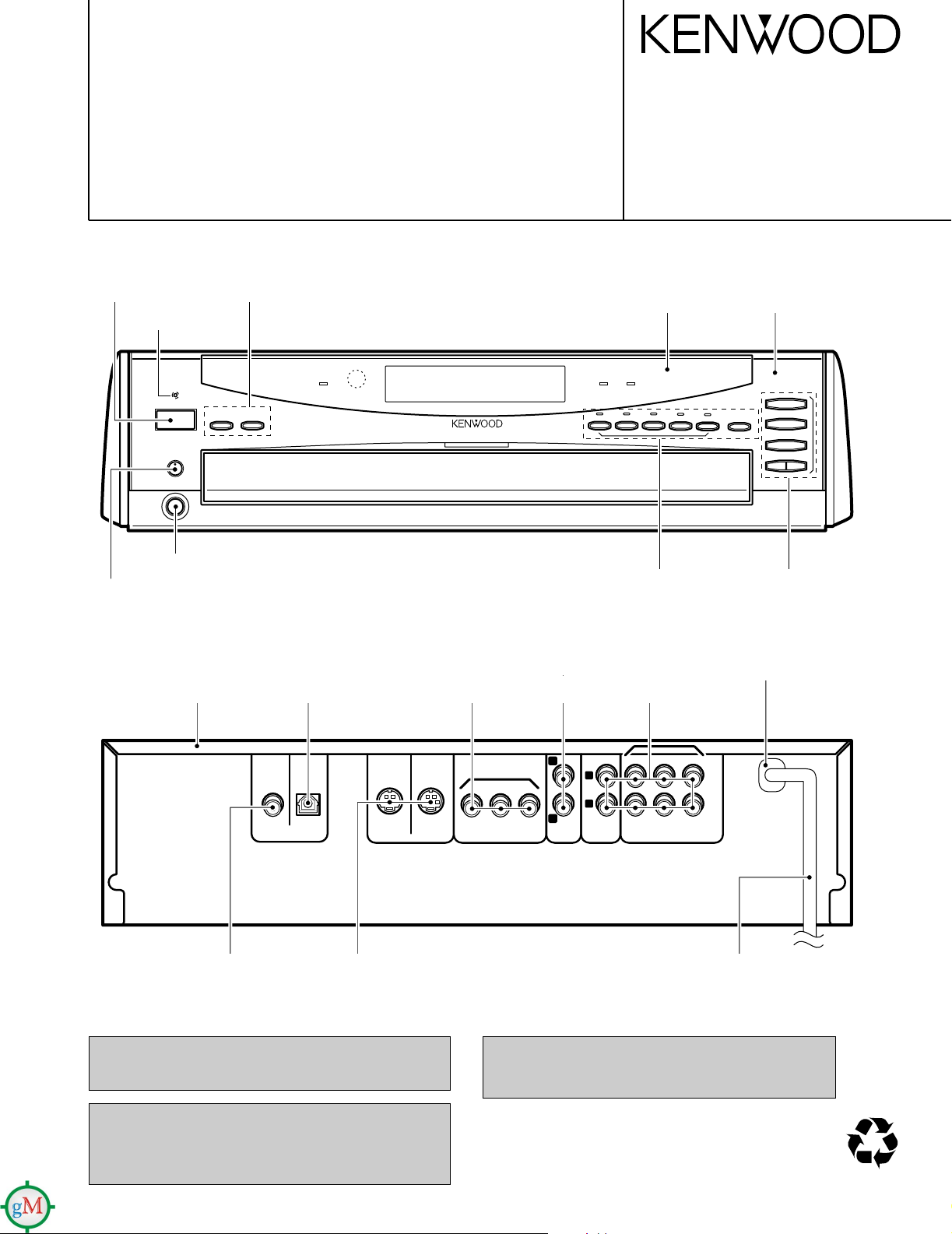
DVD VCD CD PLAYER
STANDBY
POWER
DISC SKIP
PHONES LEVEL
PHONES
MIN MAX
- ON – OFF
DISC 1
PUREAUDIO
MODE
DISC 2 DISC 3
DISC 4
DISC 5
OPEN/CLOSE
0
3
8
7
¢
4
SAMPLING
96kfs192kfs
VIRTUAL
SURROUND
0 0000 00000000000
ANGLERAMDOMPGMP.B.C.P.PCMMPEGDOLBYDTS
REPEAT TEXT
INDEX
INDEX
SEQ.1
SEQ.2
D.MIX
TOTAL
VIDEO
AUDIO
DIGITAL
DVD
CD VCD
11 2 33 44 552
AA B
3
DVD
COAXIAL OPTICAL
DIGITAL OUTPUT
(
PCM/BIT STREAM
)
SUB WOOFER
FRONT SURROUND
6CH. OUTPUT
COMPONENT VIDEO OUTPUT
YCbCr
1
2
MIX LINE
OUTPUT
VIDEO
OUTPUT
L
R
CENTER
S1 VIDEO
OUTPUT
S1/S2 VIDEO
OUTPUT
70%
DV-4070-B/4900
DVF-R7030-B/R9030
SERVICE MANUAL
Knob
(K27-2408-14)
Indicator
(B12-0399-14)
Phone jack
(E11-0190-05)
Knob
(K29-7803-04)
Knob
(K29-7194-04)
© 2000-9/B51-5665-00 (K/K) 3473
Front glass
(B10-3608-02)
Knob
(K29-7805-13)
Panel
(A60-1846-12)
Knob
(K29-7806-13)
Metallic cabinet
(A01-3759-01)
Pin jack
(E63-1128-05)
In compliance with Federal Regulations, following are reproduction of labels on, or inside the porduct relating to laser product safety.
KENWOOD-Crop. certifies this equipment conforms to DHHS
Regulations No.21 CFR 1040. 10, Chapter 1, subchapter J.
Oscillating module
(W02-2732-05)
Cylindrical receptacle
(E56-0031-05)x2
DANGER : Laser radiation when open and interlock defeated.
AVOID DIRECT EXPOSURE TO BEAM.
Pin jack
(E63-1156-05)
Caution : No connection of ground line if disassemble
Pin jack
(E63-1158-05)
AC power cord bushing
Pin jack
(J42-0083-05)
(E63-1171-05)
AC power cord
(E30-2909-05)
the unit. Please connect the ground line on
rear panel, PCBs, Chassis and some others.
Illust. is DV-4900.
Multiple DVD VCD CD
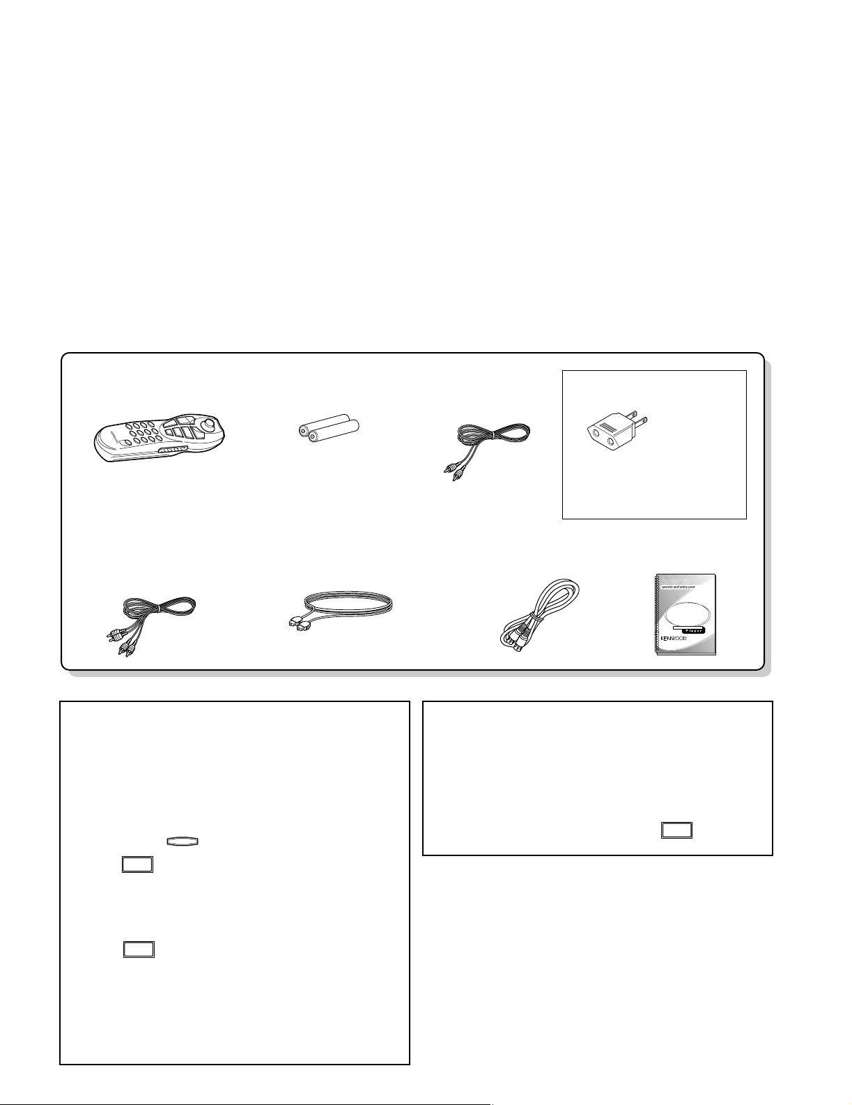
Instructoin manual/
separate User's Guide (1)
Joystick remote control unit (1)
(A70-1412-05)
Battery cover(A09-1124-08)
Batteries (R6/AA)(2) Video cable(1)
(E30-1427-05)
AC plug adapter (1)
(E03-0115-05)
Use to adapt the plug on the
power cord to the shape of the
wall outlet.
(Accessory only for regions
where use is necessary.)
S Video cable(1)
(E30-2956-05)
Audio cables(3)
(E30-0505-05)
Optical fiber cable(1)
(B19-1529-05)
DV-4070-B/4900/DVF-R7030-B/R9030
POWER
- ON – OFF
POWER
- ON – OFF
7
POWER
- ON – OFF
CONTENTS / ACCESSORIES
Contents
CONTENTS / ACCESSORIES .................................. 2
DISASSEMBLY FOR REPAIR....................................3
CIRCUIT DESCRIPTION ............................................5
ADJUSTMENT ..........................................................17
PARTS DESCRIPTIONS ..........................................18
Note: Please contact our KENWOOD Service Department in your side if you want the information;
Main Microprocessor(MN10102LP25G),Sub Microprocessor(MN101C28C) ports explanation,
D.R. I.V.E.
¿ and SCART Circuit Description and full(previous) format Parts list on this
model. You can be available them by internet from us.
Accessories
PC BOARD ...............................................................19
SCHEMATIC DIAGRAM .......................................... 23
EXPLODED VIEW ....................................................41
PARTS LIST..............................................................43
SPECIFICATIONS ....................................................54
Malfunction of Microcomputer
In case the microcomputer malfunctions, making operations
impossible or showing wrong messages on the display even
if you connected everything properly. When the microcomputer malfunctions, perform the following procedure to reset
the microcomputer and return it to the normal condition.
1. While holding on the player main unit,
press .
2. The display on the main unit shows blinking "INIT" (ini-
tializing), then shows "INIT OK!" (Initialization OK) to
indicate that the microcomputer is reset.
3. Press on the main unit to turn it off, then press
2
it again to turn it on.
¶ The resetting clears the setups stored in the microcom-
puter and returns it to the factory-set initial condition.
After resetting, you should perform the various setups
of the player again from the beginning.
Transport or moving precautions
When transporting or moving the player, first remove the
disc and observe the following procedure.
1. Turn the player power on.
2. Wait for a few seconds, until the display shows "NO
DISC".
3. Turn the player power off by pressing .
DV-4070-B/4900/DVF-R7030-B/R9030
1
5
2
3
6
4
5
HOOK ( x2)
HOOK
x2
Guide
6
3
4
HOOK
GUIDE
ARM
DRIVE
GEAR
HOOK
LOADING
GEAR (A)
(Free)
PROTRUSION OF TRAY
2
1
5
REAR
DISASSEMBLY FOR REPAIR
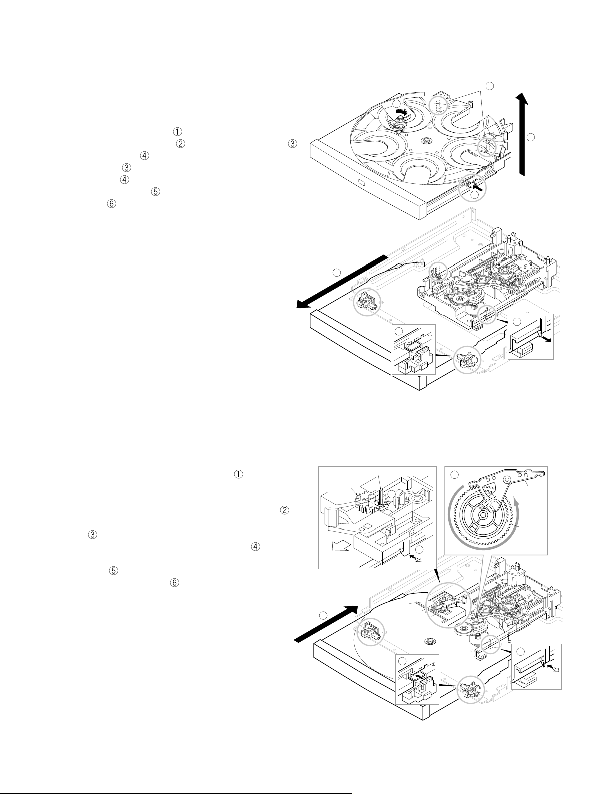
1. How to Remove Tray
1. Remove the front panel and flexible cable.
Disassemble the X25 and power supply pcb with sub
chassis if it is a difficult.
2. Push and hold the lever(
out the tray to frontwards(
meets with guide(
3. Push hooks(
from guides(
).
), both sides, inwards and release them
).
4. Pull hooks of tray(
upwards(
).
)to clockwise and pull barely
) where the hook of tray( )
) outwards and remove the tray
2. How to Assemble Tray
1. Adjust the position of drive gear as figure( ).
Check traverse unit is at the lowest position.
2. Load the tray on the loading mechanism.
Check the position where the loading gear(A) is free(
3. Meet the hooks with guides and push hooks to load the
tray(
4. Set the right side hook to loading mechanism(
5. Set the left side hook to loading mechanism with pulling it
).
outwards(
).
6. Push the tray backwards(
).
)
).
3
DV-4070-B/4900/DVF-R7030-B/R9030
2
4
2
1
3
Tray
guide
Guider
(L)
Protruding
part
5
5
5
6
6
6
X13-7770-10
CN1
CN2
Clamper weight
Spacer
Magnet
Clamper
REAR
Tilt adjustment screw 2
Tilt adjustment screw 1
Tangential adjustment screw
DISASSEMBLY FOR REPAIR
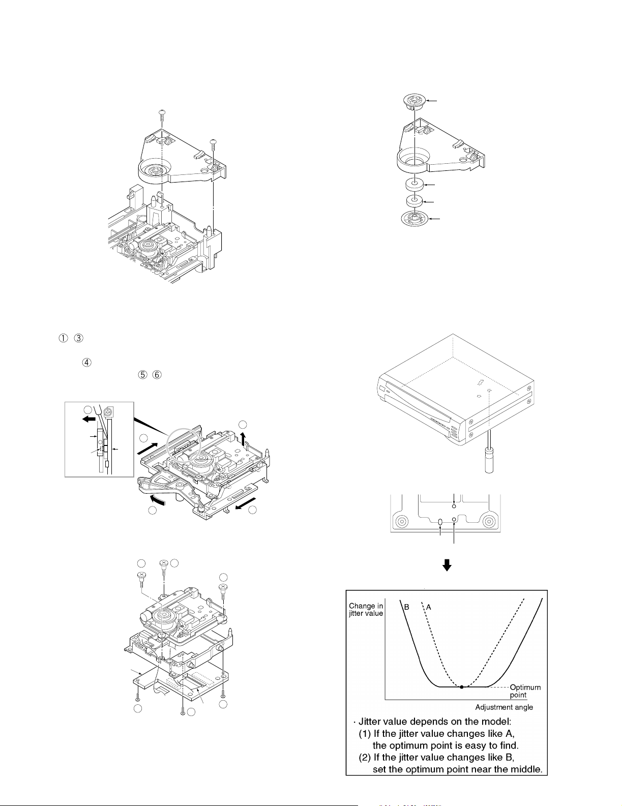
3. How to Remove Clamper Ass'y
1. Remove screws.
5. How to Disassemble Traverse Unit
1. Move the traverse to upward by turning motor pulley
(
~ ).
2. Make the gap between the tray guide and guider(L) with
driver(
3. Remove the screws(
)
, ).
4. How to Disassemble Clamper Ass'y
6. Tangential and Tilt Adjustment
1. Turn the power on with pressing the DISC 1 key.
(Display shows "INSPECTION"; test mode.)
2. Press the DISC1 key in playback mode again.
Display shows "Jitter *** %"
3. Turn off if cancel test mode.
4
DV-4070-B/4900/DVF-R7030-B/R9030
CIRCUIT DESCRIPTION
MAIN MICROPROCESSOR: MN102LP25G(X35,IC500)
Port No. Port Name I/O Description
1 WAIT O Optical Device Control(ODR) wait
2 NRD O Read(RD) port for ODC/AV
3 - - No use
4 NWA O write(WR)
5 RAMCS O Chip Select(CS) Flash RAM
6 ODCCS O Chip Select(CS) ODC
7 AVCS O Chip Select(CS) AV decoder
8 RAMCS O Chip Select(CS) DRAM for TEXT buffer
9 SCLOCK O Clock of Video DAC(ADV7172)
10 SDATA O Data of Video DAC(ADV7173)
11 FRD O Read(RD) port for Flash ROM
12 MODE2 I H: Chip Select 0, 8bit bus
13-16 CPUADR0-3 O Address A(0-3)
17 Vdd I +5V
18 SYSCLK O AV decoder HCLK
19 Vss O GND
20 XI I Clock input port
21 XO O Clock output port
22 Vdd I +5V
23 CLK I 13.5MHz clock input port
24 OSCO O No use
25 MODE2 I CPU mode: H=Memory enhanced mode
26-33 CPUADR4-11 O Address A(4-11)
34 Vdd I +5V
35-42 CPUADR12-19 O Address A(12-19)
43 Vss - GND
44 196BSY I Busy of writing jig
45 256BSY O Busy of unit
46 ATTL O Analog output attenuator L: active
47 - - No use
48 KMODE I writing mode. H=writing. L=normal.
49 AMUTE O Audio mute
50 ADSCEN I CIRC enable
51 - O No use
52 SLEEP O Front End Processor(AN8825) standby
53 FRNTH O Front DAC selector. H=front.
54 Vdd - +5V
55 FEPEN I Front End Processor SEN
56 CLKSEL O Sampling frequency selector. L=44,88,176kHz, H=48,96,192kHz
57 STBDAC2 O DAC2(AK4393) Strob
58 STBSP O Serial/parallel(NJU3711) Strob
59 STBDAC1 O DAC1(AK4393) Strob
60 ADSC O Advanced Digital Servo Control serial data transfer.
61 Vss O GND
62 - O No use
63 XS O Chip Select of E2PROM
64 SCSIEN O Enable control of writing jig. L=enable
65 DARK-DET I Video signal check by Y-signal
66 Vdd I +5V
67 SCLKO O Sub-microprocessor clock
68 SIO I Sub-microprocessor data input
69 SOO O Sub-microprocessor data output
70 SCLKI O Clock for every Ics
5
DV-4070-B/4900/DVF-R7030-B/R9030
CIRCUIT DESCRIPTION
Port No. Port Name I/O Description
71 S11 I Data input for every ICs
72 S01 O Data output for every ICs
73,74 PUP I No use. Pull up
75 NMI I Pull up.
76 ADSCINT I Interrupt of Advanced Digital Servo Control
77 ODCINT I Interrupt of Optical Device Control.
78 AVINT I AV decoder XHINT.
79 ICRST O Reset for every Ics. H=reset.
80 STBDAC3 O Standby of DAC3
81 - I Address/data mode. Pull up=address/data separate.
82 RST I Reset
83 Vdd I +5V
84-91 CPUDATA0-7 I/O Data bus(0-7)
92 Vss O GND
93-100 CPUDATA8-15 I/O Data bus(8-15)
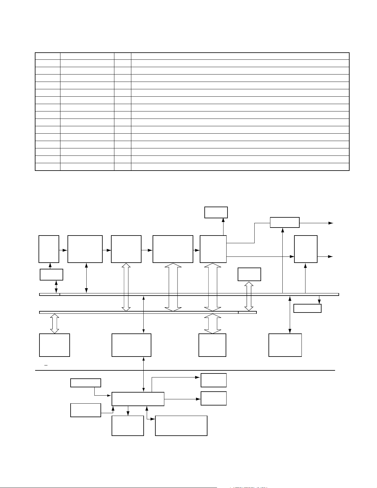
MICROPROCESSOR PERIPHERY DIAGRAM
X35,IC2 X35,IC300 X35,IC700
CONTENTS
PROTECTION
for PRERECORD
MEDIA
X25,IC102
E2PROM(4K)
MECHANISM/POWER
SUPPLY
PICKUP
ADSC
SIO1
BUS
1M
SRAM
(DVD-TEXT)
SIO0
FRONT END
PROCESSOR
8
KEY
REMOTE
CONTROL
OPTICAL
DEVICE
CONTROL
8
X35,IC500
MAIN
MICROPROCES
SOR
X25,IC100
SUB
MICROPROCESSOR
MECHANISM
16
X35,IC401/2
SDRAM
X35,IC400
AV
DECODER
FLASH
ROM(1M)
LED
X14,ED1
DISPLAY
16
WATER
MARK
X35,IC600
VIDEO DAC
X35,IC502
E2PROM(4K)
X25,IC5/6
AUDIO
DAC
X25,IC18
I/O
V. OUT
A. OUT
6
DV-4070-B/4900/DVF-R7030-B/R9030
CIRCUIT DESCRIPTION
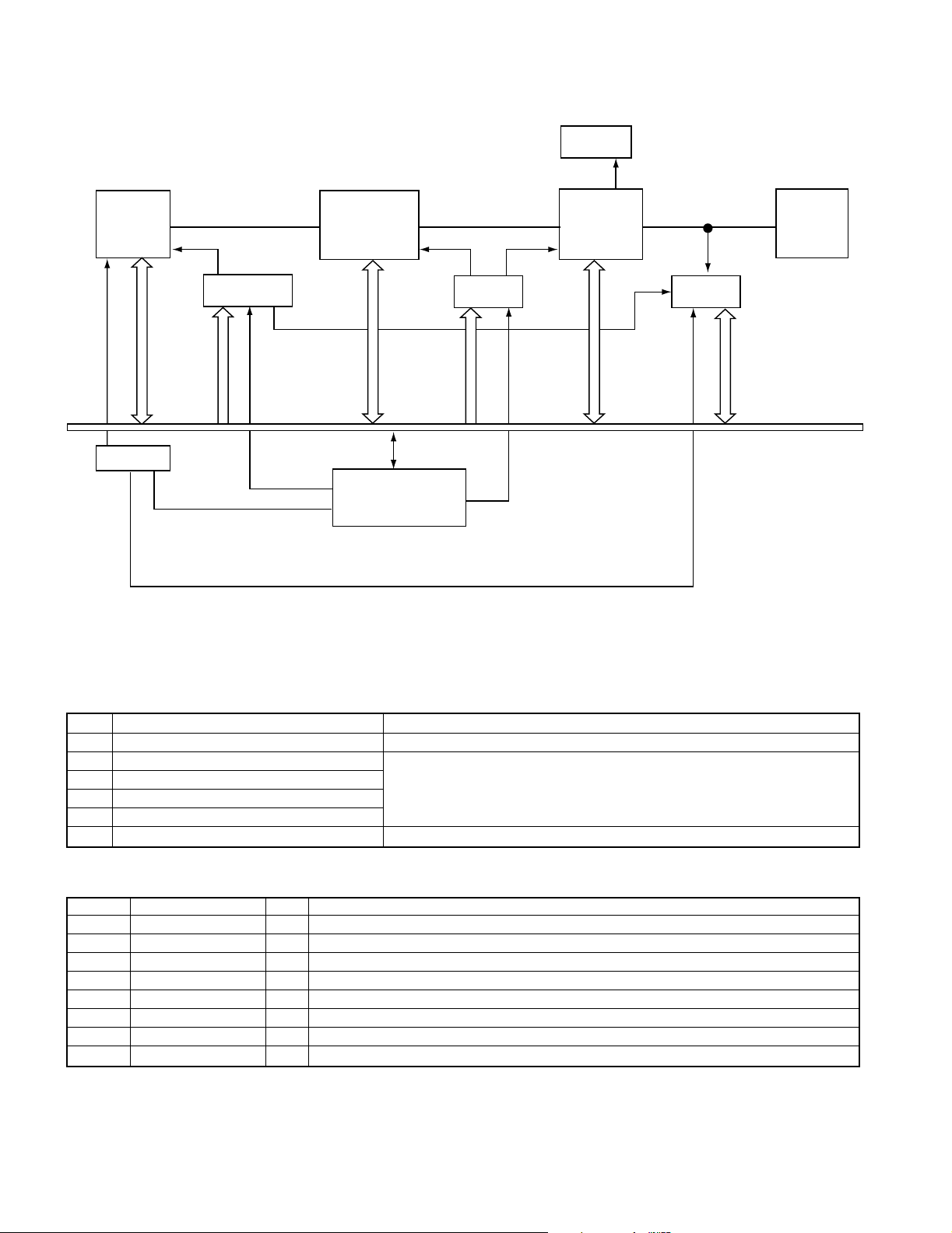
X35,IC401/2
CPPM,WM IC PERIPHERY DIAGRAM
SDRAM
BUS
X35,IC300
OPTICAL
DEVICE
CONTROL
OR
8
ADDRESS
DECODER
A19
ODCWIAT
X35,IC700
CS1
X35,IC400 X25, IC5/6
CONTENTS
PROTECTION
for PRERECORD
MEDIA
ADDRESS
DECODER
16 16
X35,IC500
MAIN
MICROPROCESSOR
A16
CS2
AV DECODER
AUDIO
DAC
WATER
MARK
8
INITIALIZATION
Turn power-on with pressing the STOP key. You can separate
from initialization mode if pull out the ac power cord.
Step function Remarks
1 POWER-ON
2 CD-TRAY CLOSE.
3 DISC-POSITION-SW ON
4 ROTARY-SW ON
Display shows blinking "INITI"
5 TRAVERSE-UNIT
6 RAM & BACKUP INITIALIZE Display shows "INITI_OK" if no trouble. "INITI_NG if any trouble.
SUB MICROPROCESSOR:MN101C28C(X25,IC100)
Port No. Port Name I/O Description
1 VREF- O Negative reference voltage for AD converter.
2-4 KEY0-2 I Key input for AD
5,6 KEY3,4 O No use
7 KISYU I Model selector
8.9 KID0,1 I Destination selector
10 VREF+ O Positive reference voltage for AD converter.
11 Vdd O +5V
12 OSC2 I Clock input,10MHz
7
DV-4070-B/4900/DVF-R7030-B/R9030
CIRCUIT DESCRIPTION
Port No. Port Name I/O Description
13 OSC1 O Clock output
14 Vss O GND
15 XI I No use
16 XO O No use
17 MMOD I GND
18 TXD0 O SIO0 data output port. Main processor contact.
19 RXD0 I SIO0 data input port. Main processor contact.
20 SCK0 O SIO0 clock
21 SB01 O SIO1 data output port. FL driver contact.
22 SB11 I SIO1 data input port. FL driver contact.
23 SCK1 I SIO1 clock
24 FLCE O FL chip enable.
25 RESET I CPU reset.
26 E2CS O No use
27 P11 O No use
28 MECHAVR O Mechanism PCM output.
29 P13 O No use
30 LED DM O No use
31 REMOCON I Remocon code input.
32 POS SEN O Mecahnism position sensor
33 MECHA FG I Mecahnism frequency generator(FG) signal input.
34 OPEN SW I Tray open switch sensor.
35 CLOSE SW I Tray close switch sensor.
36 12C SDA O IC400 control (I2C data). Scart drive/E2ROM
37 SB12 O No use
38 12C SDC O I2C clock.
39,40 P33,34 O No use
41 TM+ O Tray motor positive port.
42 TRM- O Tray/rotary motor common port.
43 RM+ O Rotary motor positive port.
44 RGBL O Y signal.
45 AOP O Video signal selector. AOP=Pure Audio Mode.
46 YCBH O H=scart color-difference signal. L=RGB.
47 TRAY OPEN O No use
48 TRAY CLOSE O No use
49 POWER O H=on. L=power off.
50 FL OFF O No use
51 WIDE1 O H=squeeze. L=letter box. L=normal.
52 WIDE2 O H=squeeze. H=letter box. L=normal.
53 C OFF O C-signal of YC-signal on/off. H=on. L=off.
54-56 P52-54 O No use
57 CE O Power chip enable.
58-60 P61-63 O No use
61-68 LED18-11 O No use
69 POWER LED O Power LED(D9).
70 96kHz O 96kHz LED(D7).
71 DISC2 O Disc 2 LED(D2).
72 DISC4 O Disc 4 LED(D4).
73 VSS LED O Vss LED(D6).
74 AOP LED O AOP LED(D15).
75 SHOWER O Shower LED(D14).
76 192kHz O 192kHz LED(D8)
77 DISC1 O Disc 1LED(D1)
78 DISC3 O Disc 3 LED(D3).
79 DISC5 O Disc 5 LED(D5).
80 POWER MUT O Power mute.
8
DV-4070-B/4900/DVF-R7030-B/R9030
X35-224
DMIX
AOUT0
AOUT1
AOUT2
DAC
DAC
DAC
DAC
IC18
H2CH
FRNTH
IC33/34
60kHz
IC31
110kHz
60kHz
60
kHz
60
kHz
IC1
D.R.I.V.E.II
L2CH
LPF
LPF
LPF
LPF
LPF
SW3
SW1
X25-637
SW2
A
B
MUTE
MUTE
MUTE
MUTE
-6dB ATT
-6dB ATT
MIX L/R
L/R
SL/SR
C/SW
MUTE Ctrl ATT Ctrl
AV1
AV2
IC32
IC4
IC5
IC6
X35-224
DMIX
AOUT0
AOUT1
AOUT2
DAC
DAC
DAC
DAC
IC18
H2CH
FRNTH
IC33/34
60kHz
IC31
110kHz
60kHz
60kHz
60kHz
IC1
IC2
IC3
D.R.I.V.E.II
D.R.I.V.E.II
D.R.I.V.E.II
L2CH
LPF
LPF
LPF
LPF
LPF
SW3
SW1
X25-637
SW2
A
B
MUTE
MUTE
MUTE
MUTE
-6dB ATT
-6dB ATT
MIX L/R
L/R
SL/SR
C/SW
MUTE Ctrl ATT Ctrl
AV1
AV2
IC32
IC4
IC5
IC6
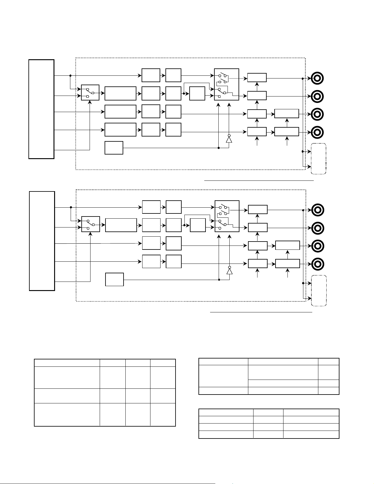
(A). DVF-R9030(J,E,T,X,M), DV-4900(K)
(B). DVF-R7030(J,E,T,X,M), DV-4070(K)
SW4
SW4
CIRCUIT DESCRIPTION
D.R.I.V.E. ¿ SIGNAL PATH
9
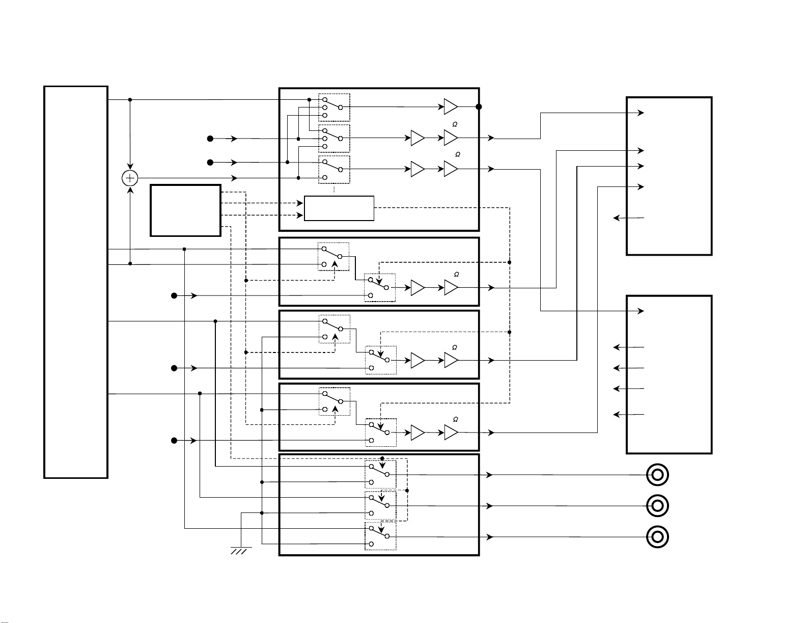
* SCART terminals(AV1,2) are available for European model
only.
Media vs SWITCHES
Media SW1 SW2 SW3
DVD-Audio
(fs: 192kHz,176.4kHz), A off on
VCD, CD-DA
Normal DVD, DTS-CD,
2-ch Speaker setting
Normal DVD, DTS-CD,
More than 3-ch Speaker A on off
setting
B on off
Low Pass Filter Media SW4
110kHz (fs:192kHz,176.4kHz)
60kHz All B
ATT Ctrl
Display ATT AV Decoder
0dB(factory setting) ON(-6dB) 0dB
±1-6dB OFF(0dB) 0 ~ -5dB, -7 ~ -12dB
DVD-Audio
Others B
-6dB * -6dB
* More than 1-ch is changed level.
A
(B). DVF-R9030(E,T), DVF-R7030(E,T)
SW1
SW2
SW3
6dB
75
Drive
6dB
75
Drive
BUF
Y(DVD)
VIN(AV2)
VIN(AV1)
IC400
I C LOGIC
2
SDA
DVDL
G/Y(DVD)
GND
GIN(AV2)
B/Cb(DVD)
BIN(AV2)
R/Cr(DVD)
C(DVD)
RIN(AV2)
SCL
YCBH
IC100
V/YOUT(19)
R/COUT(15)
GOUT(11)
BOUT(7)
VIN(20)
VOUT(19)
RIN(15)
GIN(11)
BIN(7)
VIN(20)
6dB
75
Drive
IC401
6dB
75
Drive
IC402
6dB
75
Drive
IC403
YCH
Cr
Cb
Y
IC302
SCART(AV2)
X35-224
SCART(AV1)
J8
J9
J7
SIGNAL PATH IN SCRT PCB
CIRCUIT DESCRIPTION
DV-4070-B/4900/DVF-R7030-B/R9030
10
DV-4070-B/4900/DVF-R7030-B/R9030
CIRCUIT DESCRIPTION
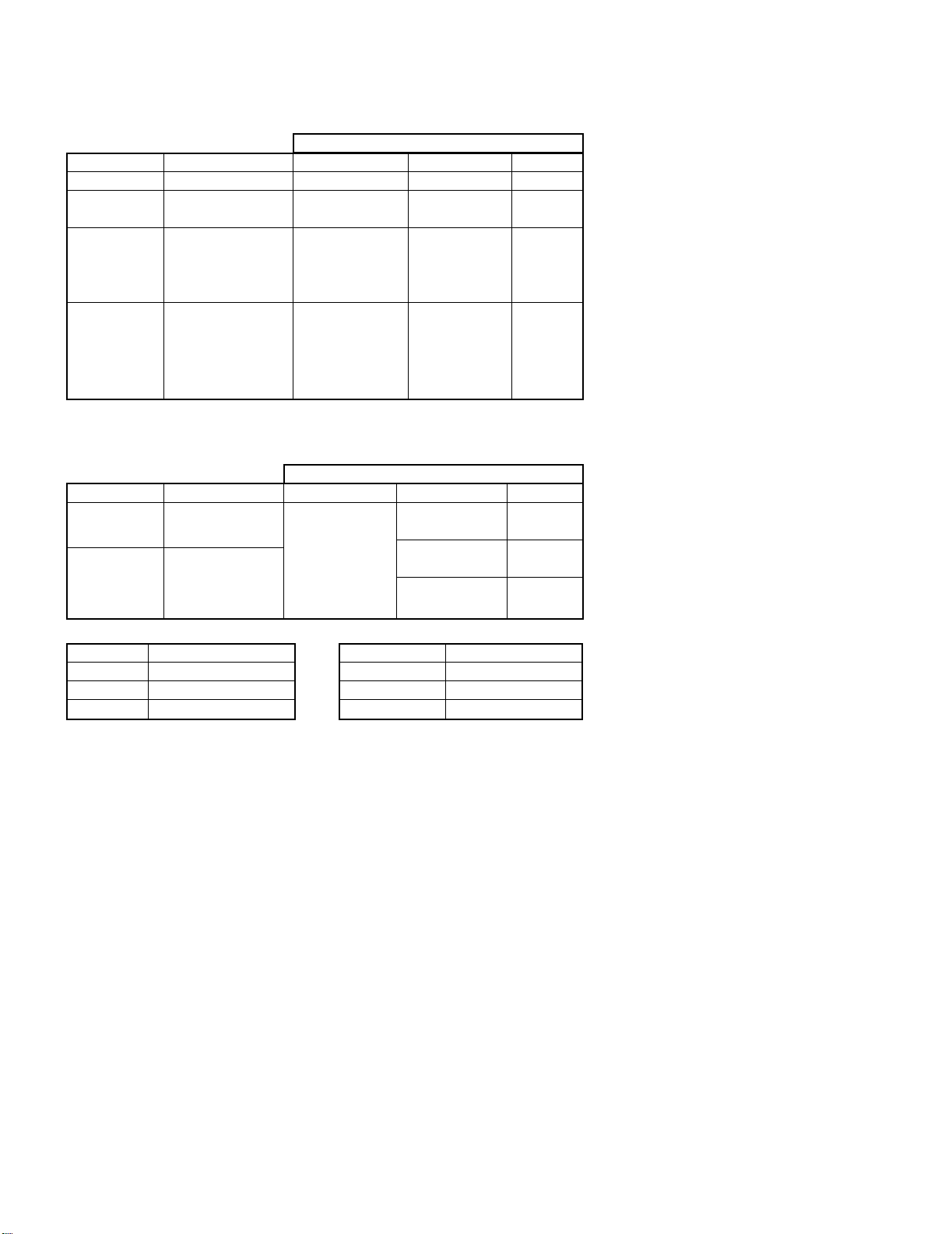
RELATION OF IN/OUT ON VIDEO SIGNAL
OUT
Condition In-SIGNAL AV1(J8) AV2(J9) RGB(J7)
Composite Y,C(IC600:X35) #19(V/Y out) #19(V out) -
S-Video Y,C(IC600:X35)
RGB RGB(IC600:X35)
<VA2>
#20(V in), #15(R/C out),
Standby #15(R in), #11(G out), IN-SIGNAL -
#11(G in), #7(B out),
#7(B in) #19(V/Y out)
#19(V/Y out),
#15(RC out)
#15(R/C out),
#11(G out),
#7(B out),
#19(V/Y out)
RELATION OF IN/OUT ON AUDIO SIGNAL
Condition In-SIGNAL AV1(J8) AV2(J9) RGB(J7)
Power on DVD MIX-OUT
#1(A[B]out), #2(A[B]in),
Standby DVD MIX-OUT
#3(A[A]out) #6(A[A]in)
--
#19(V out) -
OUT
#1(A[B]out),
#3(A[A]out)
#1(A[B]out),
#3(A[A]out)
-
-
-
Condition BLK(#16, AV1)
RGB 5V(no load)
Other 0V
Standby #16 of AV2:through
Condition FVNC SW (#8,AV1)
16:9 TV PLAY 6V
Other 11V
Standby #16 of AV2:through
11
DV-4070-B/4900/DVF-R7030-B/R9030
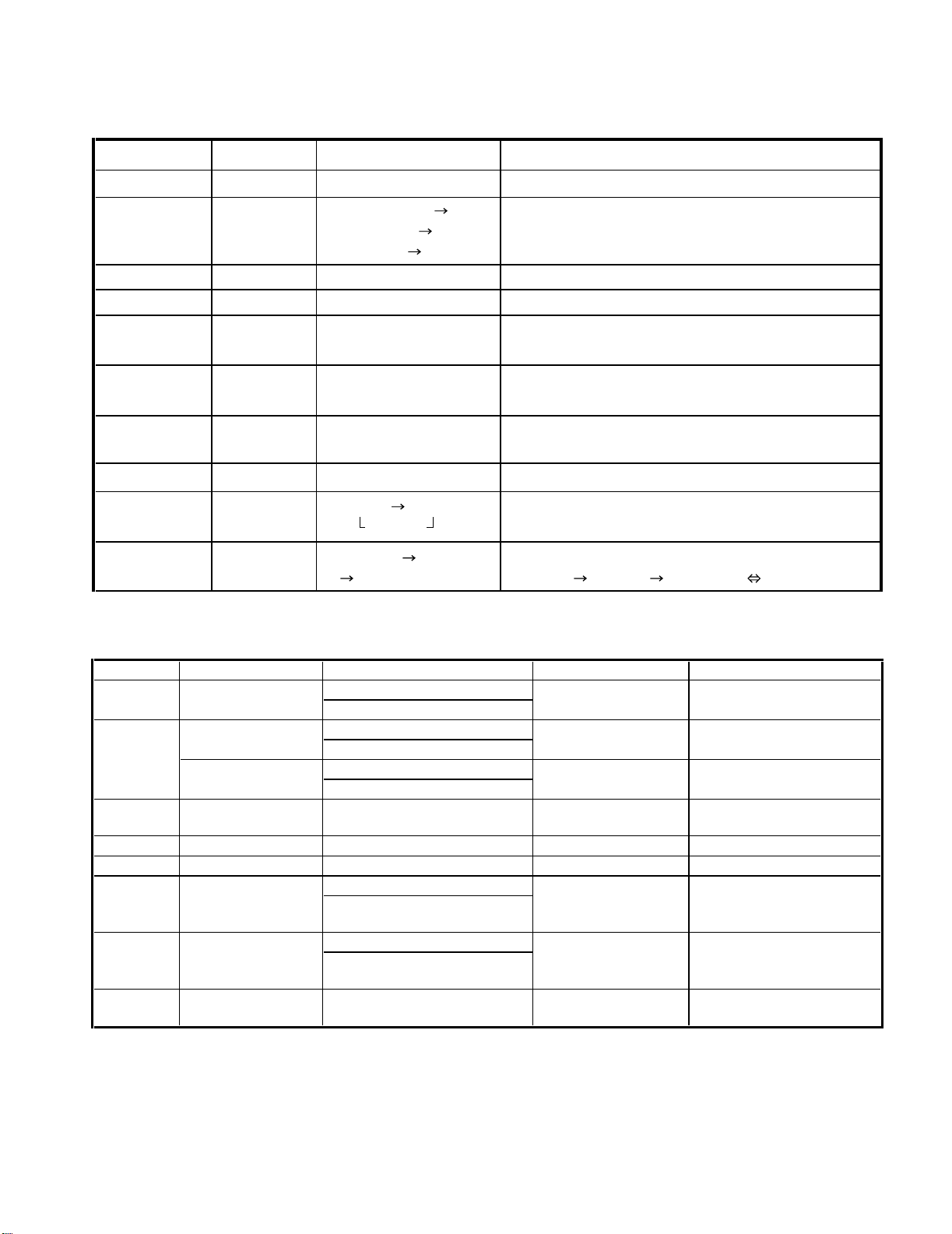
TEST MODE
Key Mode Display Operation
PLAY
-
Playback time Disc Playback
SKIP-UP
STOP
Display shows cyclically by pressing key
SKIP-UP
PLAYBACK Playback time Playback next chapter/track #/program #
SKIP-DOWN
PLAYBACK Playback time Playback before chapter/track #/program #
STOP
- Time
Stop to operate and return to first step of this
test mode.
PAUSE
Track #
Playback program-playback automatically. Order
of playback: T# 1-1
4-1 4-2 4-3 4-4 3-6.
UP/DOWN keys acceptable.
DISC1
Playback CD Track #
Playback program-playback automatically. Order
of playback: T# 2
3 7 4 16. UP/DOWN
keys acceptable.
DISC2
PLAYBACK
Mute works cyclically on or off.
DISC3
-
LPF 60k LPF 110k
Speaker protection works cyclically on or off.(Cutoff freq. Change 60k or 110k)
DISC4
-
WIDE1
WIDE2
NORMAL
WIDE mode changes cyclically WIDE1 or WIDE2.
DISC5
-
SCART RGB SCART
YC
SCART Through
Video signal of SCART changes cyclically
RGB(DVD) Y/C(DVD) Through(AV1 AV2)
OK or IC*** Self check mode(refer to Servo Error Code)
IC 100 ERROR ADSC Defective.
IC 2 ERROR FEP Defective.
IC 300 ERROR ODC Defective.
IC 400 ERROR AV DEC Defective.
STOP+DISC1
STOP Rotary turns clockwise.
STOP+DISC2
STOP Rotary turns counter clockwise.
STOP+DISC3
STOP Tray opens
STOP+DISC4
STOP Tray closes
-
DISC SKIP
CIRCUIT DESCRIPTION
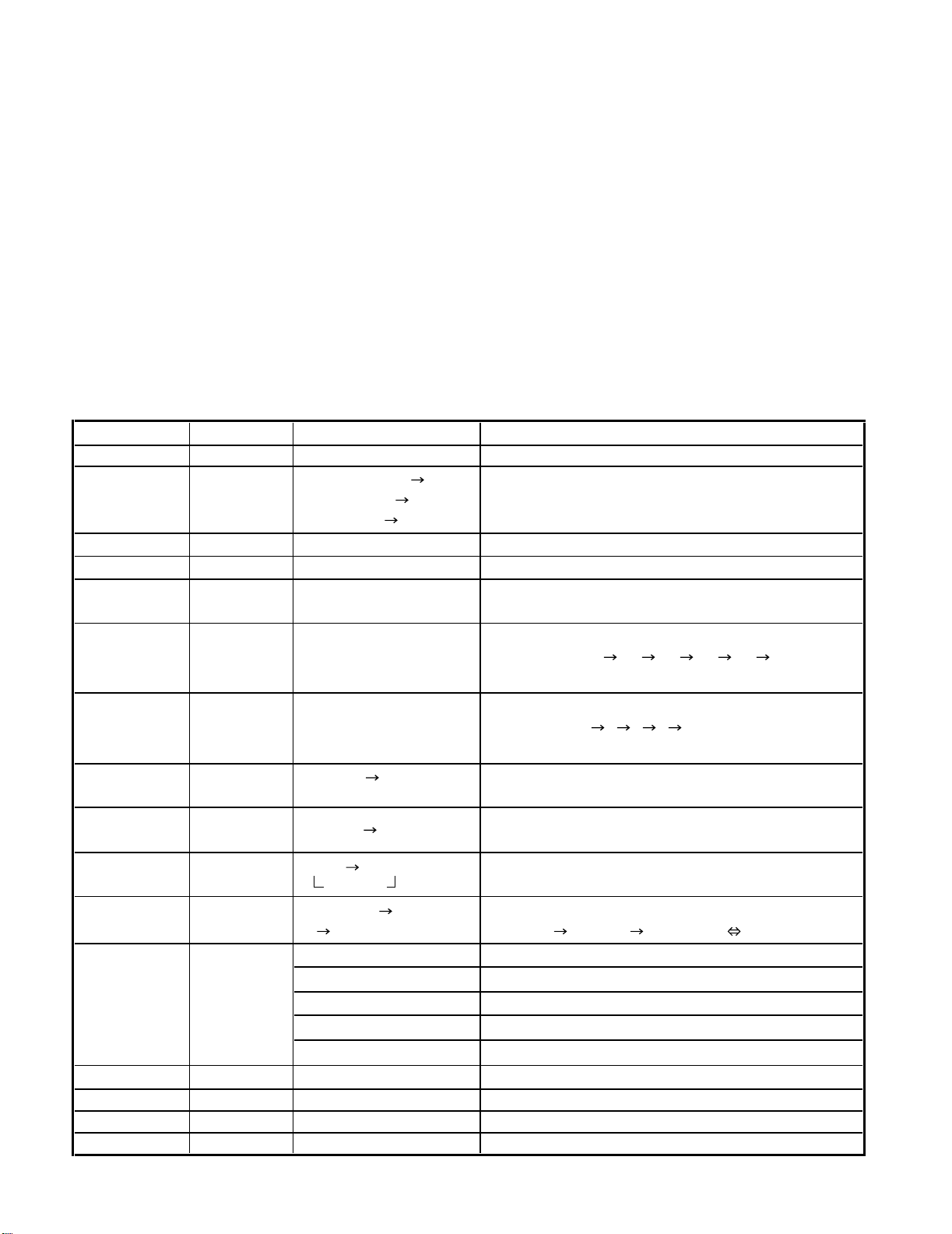
TEST MODE
This model has 3 kind of test modes; unit inspection, factory test mode, measurement. In this manual, items of repair, test
mode and inspection are available.
Setting
Turn power on with pressing "PAUSE" key. Display shows "TEST".
Turn power on with pressing "DISC1" key. Display shows "INSPECTION".
Cancellation of Setting
Turn power off.
Key vs Function
Keys which described in the following table work as it is.
Playback
DAD-VIDEO
All segments light
Niagara mode
Playback time
MUTE ON MUTE
OFF
12
DV-4070-B/4900/DVF-R7030-B/R9030
INSPECTION
Key Mode Display Operation
PLAY
- Playback time Disc Playback
SKIP-UP
STOP
Display shows cyclically by pressing key
SKIP-UP
PLAYBACK Playback time Playback next chapter/track #/program #
SKIP-DOWN
PLAYBACK Playback time Playback before chapter/track #/program #
STOP
- INSPECTION
STOP
STOP
DISC1
PLAYBACK Jitter ***%
DISC2
-
DISC4
-
WIDE1
WIDE2
NORMAL
DISC5
-
No right position of rotary
Foreign matter inserted
No right position of rotary
Foreign matter inserted
E1102
C
Disc full load
Load disc at no proper
position
No show
CLOSE
C
E1101
ERROR CODE OF MECHANISM
CIRCUIT DESCRIPTION
All segments light
Niagara mode
Playback time
Stop to operate and return to first step of this
inspection mode.
Model/destination/re
gion code
CPPM KEY ID
SCART RGB SCART
YC SCART Through
DISPLAY
E1001
E0101
No show
CONTENTS REASON CANCELING KEY
No contact with
main processor
Poor disc chucking
No cancellation of
chucking
No turn of rotary Foreign matter inserted
No open Mechanism jam
No Close Mechanism jam
Main processor doesn't work
Sio-0 bus damaged
Stop to playback and return to first step of this
test mode.
Shows jitter value(binary value vs time deviation
of PLL-clock)
15 figures.
WIDE mode changes cyclically WIDE1 or WIDE2.
Video signal of SCART changes cyclically
RGB(DVD) Y/C(DVD) Through(AV1 AV2)
OPEN/CLOSE or DIS
SKIP
CLOSE Initialization
REMARKS
No
No
No
Initialization
E0102
E0103
Playing Disc inside
No detection of disc
position
Waiting
Not stop to turn the proper
position
Foreign matter inserted at
sensor
Turn power off in open/close
mode.
OPEN/CLOSE or DIS
SKIP
NO
Remove the one disc after
turn power off
Check the sensor of discs on
the rotary.
Press the CLOSE key after
turn the power on again.
13
 Loading...