

70%
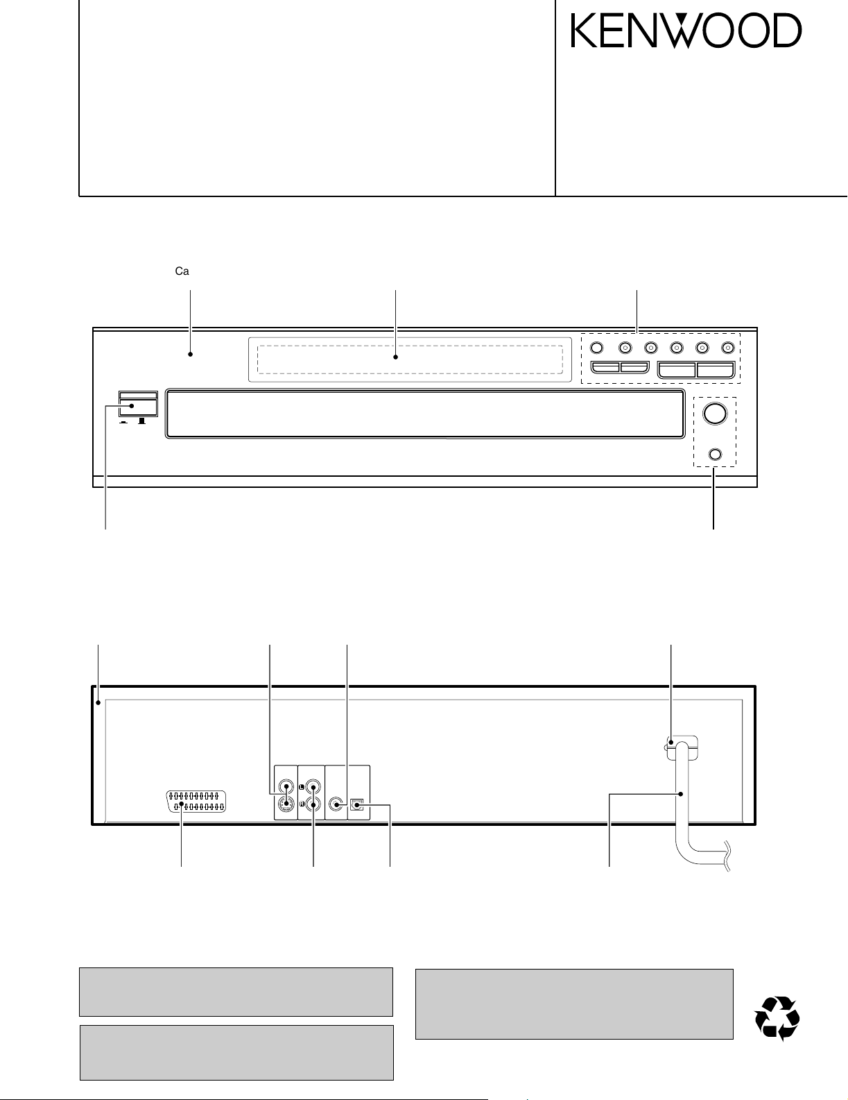
MULTIPLE DVD/VCD/CD PLAYER
76
0
POWER
ON OFF
4
¢
DISC SKIP
SEQUENCE
MODE
DISC 1
DISC 2
DISC 3 DISC 4
DISC 5
AUDIO
OUTPUT
VIDEO
OUTPUT
S-VIDEO
AV
OPTICALCOAXIAL
L
R
DVF-R5060/R5060-S
SERVICE MANUAL
© 2002-8 PRINTED IN KOREA
B51-5808-00 (K/K) 1348
This manual is available for Europe and Australia markets.
Knob(POWER) *
(K27-)
Top cover *
(A01-)
Cabinet panel *
(A60-)
Con din socket
(E68-0018-08)
Crystal Window *
(B10-)
Con phono socket
(E63-1244-08)
Button *
(K29-)
Button *
(K27-)
AC power cord bushing
(J42-0350-08)
Con scart dual
(E40-8779-08)
In compliance with Federal Regulations, following are reproduction of labels on, or inside the product relating to laser
product safety.
Caution : No connection of ground line if disassemble
the unit. Please connect the ground line on
rear panel, PCBs, Chassis and some others.
Con phono socket
(E63-1227-08)
Oscillating module
(GP1F32T)
KENWOOD Corp. certifies this equipment conforms to DHHS
Regulations No.21 CFR 1040. 10, Chapter 1, subchapter J.
DANGER : Laser radiation when open and interlock defeated.
AVOID DIRECT EXPOSURE TO BEAM.
AC power cord *
(E30-)
* Refer to parts list on page24.
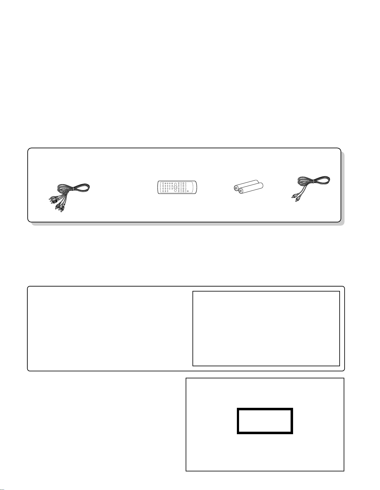
Batteries(R6/AA) ...(2)
Please confirm that the following accessories are present.
Audio video cord (Red, White, Yellow) ...(1)
(E30-2990-08)
Remote control unit ...(1)
(A70-1570-08)
Coaxial cable ...(1)
(E30-7235-08)
DVF-R5060/R5060-S
The marking of products using lasers
(For countries other than U.S.A., U.S.-Military and Canada)
The marking this product has been classified as Class 1. It
means that there is no danger of hazardous radiation outside
the product.
Location: Back panel
CLASS 1
LASER PRODUCT
Operation to reset
÷ Please note that resetting the microprocessor clears the
contents stored in, it returns the microprocessor to the condition when it left the factory.
1 In Power ON condition, keep the DISC 3 key and the 4
(Skip) key pressed at the same time.
2 When both keys are pressed, the region code of the unit,
the software version, etc. will be displayed on the display. (When nothing is done, the display of this information continues.) Example: 72. 14.02:05
3 Press the DISC 4 key and the
44
44
4 key at the same time.
"BYE" will be shown on the display.
4 Press the POWER ON/OFF switch to go to Power OFF.
5 When Power ON is performed with the POWER ON/OFF
switch, the settings become the default factory settings.
The microprocessor may fall into malfunction (impossibility to operate erroneous display, etc.) when the
power cord is unplugged while power is ON or due to
an external factor. In this case, execute the following
procedure to reset the microprocessor and return it to
normal condition.
CONTENTS / ACCESSORIES / CAUTIONS
Contents
CONTENTS / ACCESSORIES / CAUTIONS............. 2
DISASSEMBLY FOR REPAIR....................................3
BLOCK DIAGRAM ......................................................4
CIRCUIT DESCRIPTION ............................................5
PC BOARD .............................................................. 10
Accessories
SCHEMATIC DIAGRAM .......................................... 16
EXPLODED VIEW ....................................................22
PARTS LIST..............................................................24
SPECIFICATIONS ......................................Back cover
Cautions
2
DVF-R5060/R5060-S
PLASTIC
PLATE
2
3
4
4
44
1
POWER
SWITCH
LEVER
DISASSEMBLY FOR REPAIR
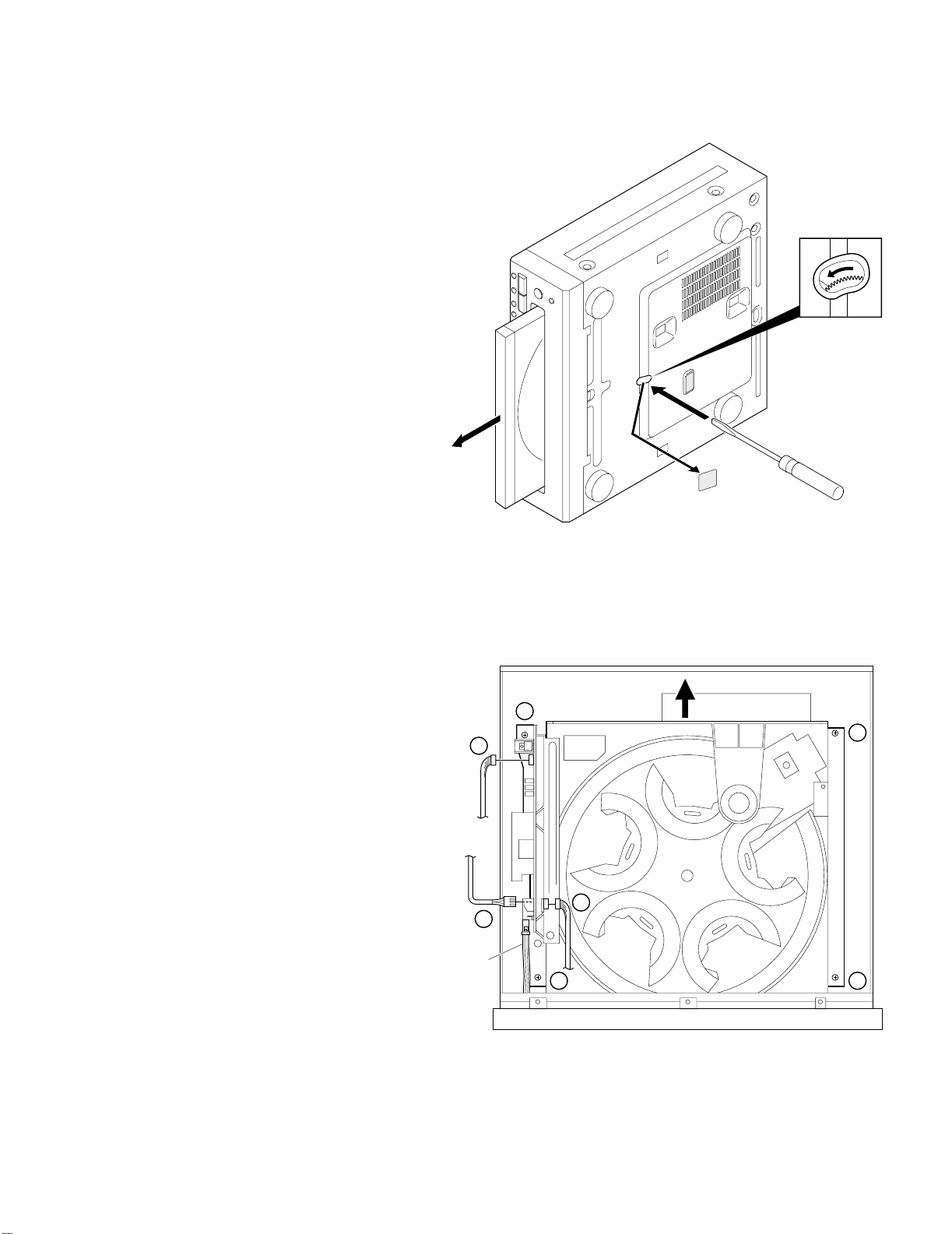
1.How to open the tray if it does not come out.
(Fig.1)
1. Remove the plastic plate.
2. Turn the gear fully CCW using a flat driver and so on in the
drawing through the hole on the loading chassis bottom.
3. Pull out the tray frontward by hand when it comes just out.
2.How to remove the DVD mechanism. (Fig.2)
1. Remove connectors (1~3) and power switch lever.
2. To separate the DVD mechanism, remove screws (4x4)
and pull it out backward.
Fig. 1
Fig. 2
3
AC CORD
+8V ANALOG VCC
-8V ANALOG VCC
+5V DIGITAL VCC
+3.3V DIGITAL VCC
+9V MOTOR VCC
5V FRONT
IC91 FL
M29W800AT
8MBIT
FLASH MEMORY
IC41
HY57V641620HGT
SDRAM-64MBIT
IC31
125MHz
IC21
MPEG
STI5519
IC32
DAC
WM8728
L.P.F
L.P.F
BA4560F
MUTE
JK82
Lch
Rch
MIXED
CVBS-VIDEO
JK83A
JK83B
S-VIDEO
Y
JK84
Cr
Cb
RCA 3V
BUFFER COAXIAL
JK81
OPTICAL
IC85
IC51
74HCU04
HEX INVERTER
IC22
EEPROM
M24C02
Q31R
Q31L
+12V ANALOG VCC
IC33
TR BUFFER
& B.N.F.
Q20S,21S
Q20Y,21Y
TR BUFFER
& B.N.F.
& B.N.F.
TR BUFFER
Q20C,21C
Q20R,21R
TR BUFFER
& B.N.F.
Q20G,21G
Q20B,21B
TR BUFFER
& B.N.F.
& B.N.F.
TR BUFFER
SCART PART
RCA PART
JK71
+5VS
FL AC
FL AC
-27V
ADDR+
F-WE
F-DE
F-RESET
ADDR+
D-RAS0-
RDNOTWR
DATA +
D-CAS0-
D-CAS1-
F-CE
F-OE(DRAM OE)
VFD DATA OUT
VFD DATA IN
+5V6S
IR REMOCON
IRQ2
+3V3-RESET
EXIT-DATA
EXIT-BCLK
EXIT-DATAVALID
EXT-PSTART/ERROR
F/E SDATA
+9V MOTOR VCC
+3.3V DIGITAL VCC
+5V DIGITAL VCC
F/E SCL
PCM1748E-DATA
PCM1748-CS
PCM1748-CLK
PCMCLK
LRCLK
BCK
AUDIO MUTE
CVBS-OUT
Y-OUT
C-OUT
GND
SPDIF
VIDEO MUTE
PIXCLK-27MHz
SDA SCL
L AUDIO
R AUDIO
F-OE(DRAM OE)
DATA +
VFD CLK
POWER CTL
VFD STB
SLIDER-OUT(DRAWER-CW-CTRL)
SLIDER-OPEN/CLOSE(POWER-POSITION-P1)
SLIDER-IN(DRAWER-CCW-CTRL)
C-OUT
Y-OUT
CVBS-OUT
G(Y)-OUT
B(Cb)-OUT
R(Cr)-OUT
G(Y)-OUT
B(Cb)-OUT
R(Cr)-OUT
Rch OUT
CVBS-OUT
BLUE-OUT
RED-OUT
GREEN-OUT
Lch OUT
SMPS
TVM MECHA
F/E & MECHA
DVF-R5060
4
DVF-R5060/R5060-S
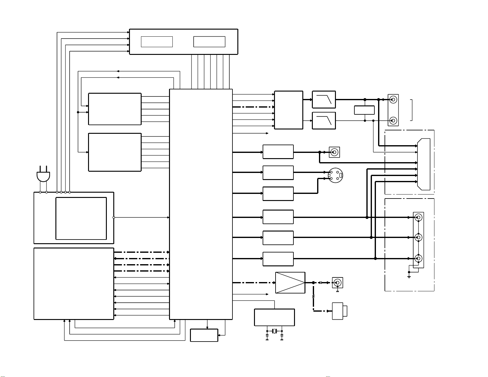
BLOCK DIAGRAM
DVF-R5060/R5060-S
CIRCUIT DESCRIPTION
1. Pin Description of MPEG Processor IC (Main, IC21)
Pin No. Pin Name I/O Pin Description
PIOs and communication
1 PIO2(5) RGB SEL(BLANK) I/O RGB sel (blank). E/T type only
2 PIO2(6) VIDEO MUTE I/O Video mute control.
3 PIO2(7) 16: 9 INDICATOR I/O 16 : 9 indicator (E/T type only)
6 PIO3(0) SCART H (TV/AUX) I/O RGB sel (blank). E/T type only
7 PIO3(1) I/O Unused.
8 PIO3(2) CSB O Unused.
9 PIO3(3) SDIN O Unused.
10 PIO3(4) IR REMOCON I/O Unused.
11 PIO3(5) SCLK O Unused.
12 PIO3(6) I/O Unused.
13 PIO3(7) DVD RESET I/O Power- on reset of front-end module.
Front-end
16 B DATA I I2S Data
17 B BCLK I I2S Bit clock
18 B FLAG I I2S Error flag
19 B SYNC I/O I2S Sector / ABS time
Reserved
20 B WCLK I/O Unused.
21 B V4 I/O Unused.
22 NRSS OUT I/O Unused.
23 VDD RGB - Supply voltage for RGB (+2.5VA).
24 VSS RGB - GND
Video DAC
25,26,27 B/G/R (OUT) O B/G/R signal outputs.
28 V REF RG I Reference voltage input for DAC RGB.
29 I REF RG I Reference current input for DAC RGB.
30 VDD YCC - Supply voltage for YCC (+2.5VA).
31 VSS YCC - GND
32~34 Y/C/CV (OUT) O Y/C/CV signal outputs.
35 V REF YCC I Reference voltage input for DAC YCC.
36 I REF YCC I Reference current input for DAC YCC.
PIOs and communication
39 PIO4(0)HP MUTE - Unused.
40 PIO4(1) - Unused.
41 PIO4(2) DAC SCKDSD O DAC system clock output.
42 PIO4(3) DAC SDIDEM O DAC data output.
43 PIO4(4) DAC MUTEB O DAC mute control.
44 PIO4(5) DAC LAT12S O DAC latch output.
45 PIO4(6) DAC CSBIWL O DAC chip select.
46 PIO4(7) ZERO I/O Zero data flag.
Audio DAC
48 VDD PCM - Supply voltage for PCM (+2V5).
49 VSS PCM - Ground for PCM.
51 DAC SCLK (BCK) O DAC over sampling clock.
52 DAC PCMOUT0 (DATA) O DAC PCM data out 0.
53 DAC PCMOUT1 O DAC PCM out 1 (unused).
54 DAC PCMOUT2 O DAC PCM out 2 (unused).
55 DAC PCMCLK O DAC PCM clock.
56 DAC LRCLK O DAC PCM Left/Right clock.
57 SPDIF OUT O Audio digital data output.
Shared memory interface
58~63 SMI ADR(4~9) O SDRAM address bus.
66~69 SMI ADR(3~0) O SDRAM address bus.
5
DVF-R5060/R5060-S
CIRCUIT DESCRIPTION
Pin No. Pin Name I/O Pin Description
70~73 SMI ADR(10~13) O SDRAM address bus.
74 SMI CS(0) O Chip select bank 0.
75 SMI CS(1) - Unused.
76 SMI RAS O SDRAM RAS
77 SMI CAS O SDRAM CAS
78 SMI WE O SDRAM write enable
79 SMI DQML O DQ MASK enable low.
80 SMI DQMU O DQ MASK enable up.
82 SMI CLKIN I SDRAM clock input.
84~93 SMI DATA(0~9) I/O SDRAM data bus.
95 SMI CLKOUT O SDRAM clock out.
97~102 SMI DATA(10~15) I/O SDRAM data bus.
Reserved
103 ADC SCLK I/O Unused.
104 ADC LRCLK I/O Unused.
105 ADC DATA I Unused.
106 ADC PCMCLK O Unused.
JTAG
109 TRST4 I Test reset from emulator module.
110 TMS I Test mode select.
111 TDO O Test data out to emulator module.
112 TDI I Test data input from emulator module.
113 TCK I Test clock input from emulator module.
Timers
114 PWM2 I/O Unused.
115 PWM1 I/O ROM boot option port (voltage low = emulator booting).
116 PWM0 I/O Unused.
EMI Interface
117 CPU OE I/O Flash ROM output enable.
118 CPU PRO CLK O SDRAM clock (unused).
Clock & Reset
120 PIX CLK I 27MHz main clock input.
122 VDD PLL - Supply voltage for PLL (+2V5).
123 VSS PLL - Ground for PLL.
124 RESET I Chip reset input.
Interrupt
125 IRQ(2) I Interrupt request 2 from front-end module.
126 IRQ(1) I Unused.
127 IRQ(0) I Unused.
EMI Interface
128 CPU BE(0) O BYTE 0 Enable
129 CPU BE(1) O BYTE 1 Enable
130 CPU RW O Unused.
131 CPU WAIT I Wait state (connected to ground).
132 CPU CE(3) O Flash ROM chip select.
133 CPU CE(2) O Flash ROM down-load JIG module select.
134 CPU CE(1) O Unused.
135 CPU CE(0) O Unused.
138 CPU RAS1 I/O Unused.
139 CPU CAS0 O Unused.
140 CPU CAS1 O Unused.
141~148 CPU DATA(0~7) I/O Flash ROM data input/output (0~7).
151~158 CPU DATA(8~15) I/O Flash ROM data input/output (8~15).
161~170 CPU ADR(1~10) O Flash ROM address (1~10).
173~183 CPU ADR(11~21) O Flash ROM address (11~21).
6
DVF-R5060/R5060-S
CIRCUIT DESCRIPTION
Pin No. Pin Name I/O Pin Description
PIOs and communication
186 PIO0(0) T STROBE I/O UART0 data
187 PIO0(1) MOD SW I/O ATAPI RD
188 PIO0(2) O VFD strobe output.
189 PIO0(3) O VFD clock output.
190 PIO0(4) O VFD data output.
191 PIO0(5) I Data input from VFD.
PIO0(6) SLIDER SENSOR
192
193
194 PIO1(0) SDA I/O SSC0 data (MTSR out / MRST in)
195 PIO1(1) SCL I/O SSC0 clock
196
197 PIO1(3) TXD(JIG) I/O UART2 TXD
200 PIO1(4) RXD(JIG) I/O UART2 RXD
201 PIO1(5) FRONT TXDI I/O UART1 TXD
202 TRIGGER IN I/O Trigger input from JIG.
203 TRIGGER OUT I/O Trigger output from JIG.
204 PIO2(0) - Unused.
205 PIO2(1) FRONT RXD I/O UART1 RXD
206 PIO2(2) I Unused.
207 PIO2(3) - Unused.
208 PIO2(4) AUDIO MUTE O Audio mute control.
Power supply
4,47,81,107
136,159,184
14,37,64,94
119,149,171
198
5,15,38,50,65
83,96,108,121
137,150,160
172,185,199
OPEN/CLOSE
(DRAWER POSITION )
PIO0(7) SLIDER IN
(DRAWER CCW/CTRL)
PIO1(2) SLIDER OUT
(DRAWER CW CTRL)
VDD3 3 - 3.3V Power supply.
VDD2 5 - 2.5V Power supply.
VSS - GND
I/O Detection port of slider sensor for DVD mechanism.
I/O Control port of slider (IN) for DVD mechanism.
I/O Control port of slider (OUT) for DVD mechanism.
7

DVF-R5060/R5060-S
CIRCUIT DESCRIPTION
2. Pin Description of IC’s
2-1 64 Bit SDRAM : HY57V641620HGT(Main, IC31)
Pin No. Pin Name I/O Description
38 CLK I
37 CKE -
19 CS - Enables or disables all inputs except CLK, CKE, and DQM.
20,21 BA0,BA1 -
22~26
29~35 Auto-precharge flag : A10
16,17,18 WE,CAS,RAS - WE, CAS and RAS define the operation.
15,39 LDQM,UDQM I/O Controls output buffers in read mode and masks input data in write mode.
2,4,5,7,8,10
11,13,42,44
45,47,48,50
51,53
1,3,9,14,27
43,49
6,12,28,41,
46,52,54
36,40 NC - Unused.
A029~35A11 -
DQ0~DQ15 I/O Multiplexed data input/output pin.
VCC/VCC Q - Power supply for internal circuits and input buffers.
VSS/VSS Q - Ground terminal.
The system clock input. all other inputs are registered to the SDRAM on the
rising edge of CLK.
Controls internal clock signal and when deactivated, the SDRAM will be one of
the states among power down, suspend or self refresh.
Selects bank to be activated during RAS activity.
Selects bank to be read/written during CAS activity.
Row address : RA029~35RA11, Column address : CA0~CA7
2-2 Flash Memory : M29W800AT(Main, IC41)
Pin No. Pin Name I/O Description
1~8, 16~25,48 A0~A18 I Address Inputs
29,31,33,35,38,40,42,44 DQ0~DQ7 I/O Data Input/Outputs, Command Inputs
30,32,34,36,39,41,43 DQ8~DQ14 I/O Data Input/Outputs
45 DQ15 I/O Data Input/Outputs or Address input
26 CE - Chip Enable
28 QE - Output Enable
11 WE - Write Enable
12 RP - Reset/Block Temporary Unprotect
15 RY/BY O Ready/Busy/Output
47 BYTE - Byte/Word Organization
37 VCC - Supply Voltage
27,46 VSS - Ground
2-3 HEX Inverter (Single Stage) : M74HCU04(IC51)
Pin No. Pin Name I/O Pin Description
1,3,5,9,,11,13 A0 to A5 I Data Inputs
2,4,6,8,10,12 Q0 to Q5 O Data Outputs
7 GND - Ground
14 VCC - Positive Supply Voltage
Truth Table
AQ
LH
HL
8

DVF-R5060/R5060-S
CIRCUIT DESCRIPTION
2-4 24-bit, 192kHz Stereo DAC : WM8728 (Main, IC32)
Pin No. Pin Name I/O Pin Description
1 LRCIN I
2 DIN I
3 BCKIN I Audio data bit clock input.
4 MCLK I Master clock input.
5 ZERO O Infinite zero detect flag.
6 DGND - Digital ground supply.
7 DVDD - Digital positive supply.
8 VOUTR O Right channel DAC output.
9 AGND - Analog ground supply.
10 AVDD - Analog positive supply.
11 VOUTL O Left channel DAC output.
12 VMID O Mid rail decoupling point.
13 VREFN - DAC negative reference.
14 VREFP - DAC positive reference.
15 CSBIWL I
16 MODE I Control mode selection.
17 MUTEB - Mute control. "L" = Mute on, "H" = Mute off
18 SDIDEM -
19 SCKDSD I
20 LAT12S I
DAC sample rate clock input : PCM input mode
Right channel DSD bitstream input : DSD input mode
Serial audio data input : PCM input mode
Left channel DSD bitstream input : DSD input mode
Software mode : 3-wire serial control chip select
Hardware mode : Input word length
Software mode : 3 or 2-wire serial control data input
Hardware mode : De-Emphasis select
Software mode : 3 or 2-wire serial control clock input
Hardware mode : DSD bitstream operation select
Software mode : 3-wire serial control load input
Hardware mode : Input data format selection
2-5 VFD Controller :CXP82532(IC91)
Pin No. Pin Name I/O Description
1 RXD I Communication from MPEG (IC21).
2 RMC IN I Input for remote control receiving circuit.
3~7 - - Unused.
8 RESET MAIN I/O System reset.
9,10 - - Unused.
11 MODE SELECT - Unused.
12,13 - - Unused.
14~18 DISC(5~1) LED I Key return input for segment signal with performs key scanning.
19~21 NC - Unused.
22 REGION - Setting of the destination.
23,24 - - Unused.
25~27 KEY1~KEY3 I Key input port.
28,29 - - Unused.
30 RST I Reset signal input.
31 EXTAL I Connection for system clock oscillation crystal.
32 XTAL O Connection for system clock oscillation crystal.
33 VSS - GND
34~56 SEG01~SEG23 O Segment signal output for FDP.
57,58 - - Unused.
59~70 G12~G1 O Grid signal output for FDP.
71 VFDP - Power supply (-25V) for FDP.
72,73 VDD - Positive power supply(+5.0V).
74 SCART H I/O 4-Bit in/output pin/Single bit addressable
75,76 - - Unused.
77 TXD O Communication to MPEG (IC21).
78,79 - - Unused.
80 - - Connected to power supply(+5V).
9

ACEG IBDFHJ
L913
L912
L909
C905
L901
L914
J902
J903
J904
J905
J906
J908
J909
J912
R904
J901
R903
C906
GGIIO
O
R950
R943
R927
C908
C904
C907 C916
C909
R926
R946
X901
J914
J915
J916
J917
J918
J919
J923
J926
R945
J913
5428161
C911
R933
R921
R985 R984 R983 R982 R981
J920
J921
DISC SKIP
REWARD SKIP
FORWARD SKIP
DISC 1
DISC 2
J922
DISC 3
STOP
PLAY/PAUSE
R911
R912
R923
R922
R931
R913
J924
DISC 4
DISC 5
J925
J927
J928
LUG2
R932
R938
C903
R940
R939
R902
R901
J907
J911
J910
C901
R906
R905
LUG1
D906
DL95
S911
S915
S917
S921
S901
SEQUENCE MODE
OPEN/CLOSE
S913
S930
S903
S924
S927
S907
CN93
S905
DL94 DL93 DL92
DL91
D907
CN91
CN92 SCN1
IC92
RM91
FL91
BE
Q915
BE
Q914
BE
Q913
BE
Q912
BE
Q911
1
1351
1
5
CP95
1
5
CP94
CONNECTION BOARD
FRONT BOARD
1
5
3
1
CN93
3
1
24
64
65
80
40
25
41
IC91
C005
R003
1
12 1
1
1
1
1
2
11
12
1
2
11
12
6
2
2
110
110
6
C002
JW18
JW8
R004
L001
JW15
JW20
C001
JW10
C003
C004
JW22
JW14
R002
JW7
R001
JW3
JW21
JW6
JW17
JW13
JW24
IC001
P003
MECHA CONTROL BOARD
P406
PI001
PI002
P004
P406B
PI004
CAROUSEL MOTOR BOARD
PI003
P027
CP210
CP211
D001
D002
IC002
R805
123
C804
R806
R804
R815
C801
R801
R802
R807
C803
R808
R820
C817R
R873
R872
R876
R877
R874
R829
R865
R803
R863
PAL OPTION
R864
R87L
R87R
R875
J892
J894
EB
Q801
BE
Q815
EB
Q802
R719
R717
C716
R718
R708
R709
C717
R720
R721
R705
R722 C718
R702
R730
R723
L706
L703
R714
R715
C17
J891
D710
D705
D706
D709
D708
D707
D701
D702
E
Q702
BE
Q704
C821
L705
R716
R731
R734
R701
J890
BE
Q701
R724
L704
B
C802
1
2
23
22
C822
J005
J004
C720
J17
J58
J3
J14
J40
J9
121
220
21
J2
C719
C703
J736
J13
L
R
L801
J10
J11
J16
J6
J57
C714
C713
LUG701
L804
J1
D711
CN01
JK83
JK84
IC85
JK81
JK71
JK82
C715
OUTPUT BOARD
OPTICAL
DIGITAL OUT
COAXIAL
OUTPUT
AUDIO
OUTPUT
VIDEO
OUTPUT
VIDEO
COMPONENT
PC BOARD (Component side view)
1
2
3
4
5
6
7
Refer to the schematic diagram for the value of resistors and capacitors.
11
10

K LNPRTMOQS
R21P
IGO
1
12
1
2
23
22
R38L
1
1
2854
271
17
14
8
10
20 11
4
85
C20S
C327
C325
C323
C210
C206
C204
C232
C233
C21P
C36L
C36R
C35R
C35L
C331
C31L
C31R
C20C
C23C
C23S
C25S
C24S
R23S
R22S
C25C
C24C
R23C
R22C
C22C
R21C
R25C
R24C
C21C
C22Y
C23Y
R21Y
R25Y
R24Y
C21Y
C22R
R21R
R25R
R24R
C21R
C22G
R21G
R25G
R24G
C21G
C22B
R21B
R25B
R24B
R27B
R27G
R27R
R221
C20B
C23B
C23G
C23R
C20R
C20Y
C20G
R270
R269
C226
C227
R263
R262
R409
R223
C21B
C25B
C24B
R23B
R22B
C25Y
C24Y
R23Y
R22Y
C25R
C24R
R23R
R22R
C25G
C24G
R23G
R22G
C22S
R21S
R25S
C21S
R24S
R38R
C37L
C37R
R37L
R257
R27S
R27C
R27Y
C235
R271
R201
R204
R203
R268
R267
R282
R283
R421
R422
R423
R424
R425
C241
R285
R236
C503
R503
R502
C502
R314
L501
C505
X501
C215
C240
C501
C406
C221
C218
R501
R256
R402
RA41RA42RA43RA44
C239
C238
C237
R250
R228
GND1
R279
R280
R281
C217
R248
R249
C504
C216
R246
R247
R426
R237
R240
R289
R290
R239
R231
R213
R328
R234
R232
R233
R220
R214
R219
R207
R208
R218
R215
R26Y
1
52
156
241
25
48
157
208
8
5
104
1
1
5
15
14
2
12
1
53
105
C33R
C332
R34R
C32R
R31R
R34L
C33L
R323
R322
C32L
R31L
R33L
R32L
R33R
R32R
R26C
R26S
R327
R26B
R26G
R26R
R238
R288
R241
R403
R401
RA48
RA47
RA46RA45
RA34
RA35
RA36RA37
RA31
RA32RA33
R243
R244
R245
R251
R303
R304
R305
R306
R307
R308
R427
R428
R405
R406
R438
C230
C229
C228
R273
R274
R266
4
1
1
19
18
2
C225
R298
C234
R202
R222
R292
R291
R39L
R39R
R37R
R325
J208
J207
R474
J204
J203
D303
CP25
C
E
C
E
C
E
C
E
C
E
C
E
Q20G
Q20B
Q20R
Q20Y
Q20C
Q20S
BE
Q201
BE
Q202
BE
Q203
BE
Q301
D302
BE
Q32L
BE
Q31R
IC23
IC33
IC32
CN25
MAIN BOARD (SIDE A)
EB
Q21S
EB
Q31L
EB
Q21C
EB
Q21Y
EB
Q21R
EB
Q21G
EB
Q21B
IC22
CP21
IC21
CP23
CN26
CN21
IC41
IC31
IC51
J202 J201
L301
L211
C311
D301
CN27
HCN1
PC BOARD (Component side view)
1
Refer to the schematic diagram for the value of resistors and capacitors.
2
3
4
5
6
7
1312

UWYAAACVXZABAD
CP22
R28S
R28C
R20C
R20S
R28Y
R20Y
R28R
R20R
R28G
R20G
R28B
R20B
J301
L210
CVBS SIG
C SIG
Y SIG
R(Cr) SIG
G(Y) SIG
B(Cb) SIG
L20S
L20Y
L20C
L20R
L20G
L20B
C312
C205
L202
L201
L208
L209
L302
L203
C203
C201
R265
R264
C224
C403
C402
R410
R408
R407
C401
C223
C322
R326
R321
C324 C326
R302
R301
R309
C222
C220
R255
R415
L206
L205
L204
C405
1
15
14 2
R254
C208
R216
C207
R313
C211
C321
C212
C213
C214
C333
C329
C334
C328
C335
C209
R230
R212
R209
R205
C202
R315
R242
R413
R311
R310
R312
R404
R252
C219
C245
C244
C243
C242
C404
R429
R430
R431
R432
R433
R434
R435
R436
R437
R253
MAIN BOARD (SIDE B)
PC BOARD
1
2
3
Component side view
(
)
4
5
6
7
Refer to the schematic diagram for the value of resistors and capacitors.
14 15

A BDFHJCEG I
156
155
154
153
152
151
150
149
148
147
146
145
144
143
142
141
140
139
138
137
136
135
134
133
132
131
130
129
128
127
126
125
124
123
122
121
120
119
118
117
116
115
114
113
112
111
110
109
108
107
106
105
104
103
102
101
100
99
98
97
96
95
94
93
92
91
90
89
88
87
86
85
84
83
82
81
80
79
78
77
76
75
74
73
72
71
70
69
68
67
66
65
64
63
62
61
60
59
58
57
56
55
54
53
1
2
3
4
5
678
9
10
11
12
131415
1617181920
21
22
232425
2627282930
31
32
333435
36
37
383940
41
42
434445
4647484950
51
52
157
158
159
160
161
162
163
164
165
166
167
168
169
170
171
172
173
174
175
176
177
178
179
180
181
182
183
184
185
186
187
188
189
190
191
192
193
194
195
196
197
198
199
200
201
202
203
204
205
206
207
208
CPU DATA(13)
CPU DATA(12)
CPU DATA(11)
CPU DATA(10)
CPU DATA(9)
CPU DATA(8)
VSS
VDD2 5
CPU DATA(7)
CPU DATA(6)
CPU DATA(5)
CPU DATA(4)
CPU DATA(3)
CPU DATA(2)
CPU DATA(1)
CPU DATA(0)
CPU CAS1
CPU CAS0
CPU RAS1
VSS
VDD3 3
CPU CE(0)
CPU CE(1)
CPU CE(2)
CPU CE(3)
CPU WAIT
CPU RW
CPU BE(1)
CPU BE(0)
IRQ(0)
IRQ(1)
IRQ(2)
RESET
VSS PLL
VDD PLL
VSS
PIX CLK
VDD2 5
CPU PROCLK
CPU OE
PWM0
PWM1
PWM2
TCK
TDI
TDO
TMS
TRST
VSS
VDD3 3
ADC PCM CLK
ADC DATA
ADC LRCLK
ADC SCLK
SMI DATA(15)
SMI DATA(14)
SMI DATA(13)
SMI DATA(12)
SMI DATA(11)
SMI DATA(10)
VSS
SMI CLK OUT
VDD2 5
SMI DATA(9)
SMI DATA(8)
SMI DATA(7)
SMI DATA(6)
SMI DATA(5)
SMI DATA(4)
SMI DATA(3)
SMI DATA(2)
SMI DATA(1)
SMI DATA(0)
VSS
SMI CLK IN
VDD3 3
SMI DQMU
SMI DQML
SMI WE
SMI CAS
SMI RAS
SMI CS(1)
SMI CS(0)
SMI ADR(13)
SMI ADR(12)
SMI ADR(11)
SMI ADR(10)
SMI ADR(0)
SMI ADR(1)
SMI ADR(2)
SMI ADR(3)
VSS
VDD2 5
SMI ADR(9)
SMI ADR(8)
SMI ADR(7)
SMI ADR(6)
SMI ADR(5)
SMI ADR(4)
SPDIF OUT
DAC LRCLK
DAC PCM CLK
DAC PCM OUT2
DAC PCM OUT1
PIO2(5) RGB SEL
PIO2(6) VIDEO MUTE
PIO2(7) 16:9
VDD3 3
VSS
PIO3(0) SCART H
PIO3(1)
PIO3(2)
PIO3(3)
PIO3(4) IR(REMOCON)
PIO3(5)
PIO3(6)
PIO3(7) DVD RESET
VDD2 5
VSS
B DATA
B BCLK
B FLAG
B SYNC
B WCLK
B V4
NRSS OUT
VDD RGB
VSS RGB
B OUT
G OUT
R OUT
V REF RG
I REF RG
VDD YCC
VSS YCC
Y OUT
C OUT
CV OUT
V REF YC
I REF YC
VDD2 5
VSS
PIO4(0)
PIO4(1)
PIO4(2) DAC SCKDSD
PIO4(3) DAC SDIDEM
PIO4(4) DAC MUTEB
PIO4(5) DAC LAT125
PIO4(6) DAC CSBIWL
PIO4(7) DAC ZERO
VDD3 3
VDD PCM
VSS PCM
VSS
DAC SCLK (BCK)
DAC PCM OUTO (DATA)
CPU DATA(14)
CPU DATA(15)
VDD3 3
VSS
CPU ADR(1)
CPU ADR(2)
CPU ADR(3)
CPU ADR(4)
CPU ADR(5)
CPU ADR(6)
CPU ADR(7)
CPU ADR(8)
CPU ADR(9)
CPU ADR(10)
VDD2 5
VSS
CPU ADR(11)
CPU ADR(12)
CPU ADR(13)
CPU ADR(14)
CPU ADR(15)
CPU ADR(16)
CPU ADR(17)
CPU ADR(18)
CPU ADR(19)
CPU ADR(20)
CPU ADR(21)
VDD3 3
VSS
PIO0(0) T STROBE
PIO0(1) MOD SW
PIO0(2)
PIO0(3)
PIO0(4)
PIO0(5)
PIO0(6) SLIDER SENSOR OPEN/CLOSE(DRAWER POSITION PI1)
PIO0(7) SLIDER IN(DRAWER CCW CTRL)
PIO1(0) SDA
PIO1(1) SCL
PIO1(2) SLIDER OUT(DRAWER CW CTRL)
PIO1(3) TXD(JIG)
VDD2 5
VSS
PIO1(4) RXD(JIG)
PIO1(5) FRONT TXDI
TRIGGER IN
TRIGGER OUT
PIO2(0)
PIO2(1) FRONT RXD
PIO2(2)
PIO2(3)
PIO2(4) AUDIO MUTE
1
2
3
4
5
6
7
8
9
10
11
12
13
14
15
16
17
18
19
20
21
22
23
24
A15
A14
A13
A12
A11
A10
A9
A8
NC
NC
WE
RP
NC
NC
RY/BY
A18
A17
A7
A6
A5
A4
A3
A2
A1
48
47
46
45
44
43
42
41
40
39
38
37
36
35
34
33
32
31
30
29
28
27
26
25
A16
BYTE
VSS
DQ15
DQ7
DQ14
DQ6
DQ13
DQ5
DQ12
DQ4
VCC
DQ11
DQ3
DQ10
DQ2
DQ9
DQ1
DQ8
DQ0
OE
VSS
CE
A0
1
2
3
4
E0
E1
E2
VSS
8
7
6
5
VDD
WC
SCL
SDA
RA45 47
161
162
164
163
167
168
166
165
RA46 47
178
176
177
175
173
174
RA48 47
170
169
RA47 47
R407 47
R408 47
R410 47
R409 47
179
180
182
181
R263 47
R262 47
188
189
191
190
196
193
192
R289 47
R290 47
197
200
186
187
R264 75
R265 75
202
203
157
158
RA44 47
155
156
151
154
152
153
RA43 47
142
145
148
146
147
RA42 47
143
144
RA41 47
141
148
147
145
146
143
144
141
142
R401 47
R402 47
R256 47
R403 47
100u10
+
C221
0.01
C220
10
R254
0.1
C219
47
0.1
C222
10K
R255
R288 10K
10K
113
112
111
110
109
0.1
C218
115
0.1
C223
10K
47
133
128
0
J301
+3.3V
R309 100
R308 100
R307 100
R306 100
R305 100
R303 100
R304 100
R302 100
R301 100
4.7K
R310
4.7K
R311
R234 47
R233 100
10P
C213
3
1
6
47247
47
0.1
C201
R292
R203 100
R204 100
R201 100
R202 100
161918
17
13
C202
0.1
100u10
+
C204
0.01
C203
2.2uH
L201
R205
100u10
C206
+
0.01
C205
L202
2.2uH
R26G 270
R26R 270
R26B 270 R26Y 270
R26C 270
R26S 270
R209
R27Y 10
R27C 10
R27S 10
C207
0.1
R215 47
R214 47
R213 47
0.01
C209
100u10
+
C210
L203
2.2uH
R230
0
C208
0.1
47
R232
10P
C211
47
R231
10P
C212
34
33
32
44
45
46
25
26
27
51
52
+3.3V
+2.5V
R253R252
R404
R251
117
128
132
R223 47
208
1
2
3
4
5
6
7
8
9
10
11
12
13
14
15
16
17
18
19
D GND
SECTOR START
DATA VA LID
DATA(EXT DATA)
BIT CLOCK(EXT BCLK)
D GND
RESET(3V3 RESET)
DXX INTERRUPT(IRQ2)
SCL
SDA
D GND
M GND
+3.3V
+5VD
D GND
A GND
+9VM
1
2
3
4
5
RESET MAIN
FRONT TXD
FRONT RXD
OPTION NC
+5V6S
15
14
13
12
11
10
9
8
7
6
5
4
3
2
1
158
148
147
157
155
145
146
156
152
141
142
151
153
143
144
154
117
161
132
162
163
165
164
166
167
168
180
181
182
175
169
170
173
174
177
176
178 179
128
47K
R413
+
C406
100u10
1.8K
R270
1.8K
R269
0.1
C225
47
R268
47
R267
10
R266
17
16
18
19
0
J204
0
J203
R273 100
R274 100
68P
C226
0.1
C234
68P
C227
13
10K
R406
10K
R405
186
141
142
148
145
143
144
147
146
117
133
128
187
0.1
C401
C402
0.1
0.1
C403
0.1
C224
+5V
+12V
+9V
1K
R250
0.1
C217
4.7K
R246
4.7K
R247
10K
R248
470P
C216
117
12
12
+3.3V
+5V
+9V
+3.3V
+5V
+12V
+5V
+12V
+9V
+3.3V
+2.5V
+3.3V
+5V
+2.5V
+3.3V
+5V
+3.3V
+2.5V
+3.3V
+2.5V
+2.5V
+3.3V+3.3V
+2.5V
+5V
+3.3V
+2.5V
+3.3V
+2.5V
+3.3V
C405
1000P
C404
1000P
+
C228
47u16
+
C229
47u16
+
C230
47u16
L204
L205
L206
2.2uH
L209
470u6.3
C233
+
R27R 10
R27B 10
R27G 10
19
14
16
18
17
15
13
12
11
10
9
8
7
6
3
5
4
2
1
19
14
16
18
17
15
13
12
11
10
9
8
7
6
3
5
4
2
1
NC
R216 4.7K
+5.6V
1K
R228
L211
0.1
C235
1K
R257
R271
4.7K
100
R221
10
R438
C241 33P
C240 100P
C238 100P
C239 100P
C237 100P
R279 0
R282 47
R283 47
R285 47
10K
R281
10K
R280
10K
R298
1
1
4
12
10
11
9
7
8
5
6
2
3
1
R421 47
R422 47
R424 47
R423 47
R428 47
R427 47
R426 47
R425 47
R436 47K
R435 47K
R433 47K
R434 47K
R432 47K
R430 47K
R431 47K
R429 47K
192
193
1967190
189
188
191
0
R437
ROU MO-
ROU MO+
DISK SEN
ROU SEN
ID MO+
OPEN SEN
ID MO-
CLOSE SEN
+12V MOTOR
M GND
M GND
+5VD
R291
R222
7
+3.3V
100u10
+
C232
C243
10P
10P
C242
C245
10P
C244
10P
+9VM
+5V
+5.6V
+12V
R474
2.2
1/2W
41
42
43
R220 47
R219 47
R218 47
+9V
+12V
+5V
+5V
+12V
+5V
+5V +5V
0
R412
18K
18K
+2.5V
R212 4.7K
(LRCIN)
(MCLK)
OPTION
R415
0
L208
IC21
IC41
IC22
MAIN BOARD
CP21
CN21
CP22
Q201 Q202
MECHA
F/E BOARD
Q203
D303
CN26
(E,ES)
TYPE
FLASH MEMORY
EEP ROM
MPEG
B
A
ONLY
3.7V
5.3V
1
2
3
4
5
6
7

TKMOQSLNPR
1
2
3
4
5
6
7
8
9
10
11
12
13
14
15
16
17
18
19
20
21
22
23
24
25
26
27
VCC
DQ0
VCC Q
DQ1
DQ2
VSS Q
DQ3
DQ4
VCC Q
DQ5
DQ6
VSS Q
DQ7
VCC
LDQM
WE
CAS
RAS
CS
BA0
BA1
A10
A0
A1
A2
A3
VCC
54
53
52
51
50
49
48
47
46
45
44
43
42
41
40
39
38
37
36
35
34
33
32
31
30
29
28
VSS
DQ15
VSS Q
DQ14
DQ13
VCC Q
DQ12
DQ11
VSS Q
DQ10
DQ9
VCC Q
DQ8
VSS
NC
UDDM
CLK
CKE
NC
A11
A9
A8
A7
A6
A5
A4
VSS
1
2
3
4
5
6
7
14
13
12
11
10
9
8
RA36 47
RA37 47
RA34 47
RA35 47
4.7K
R312
4.7K
R313
76
74
77
78
79
80
82
RA33 47
RA32 47
RA31 47
10P
C214
+2.5V
102
101
100
99
93
92
97
98
89
88
90
91
87
84
86
85
69
68
71
70
62
67
66
63
59
58
60
61
+2.5V
+3.3V
+2.5V
73
72
1
2
3
4
5
6
7
8
9
10
11
12
13
14
15
TRGI OUT
TRGI IN
GND(OPTION)
TMS
GND
TCK
GND
TDI
GND
TDO
+5VD
TXD(JIG)
RXD(JIG)
JTAG RST
TRST
1
2
3
4
5
6
7
8
9
10
11
12
+9V
A GND
-9V
+12V
+3V5D
D GND
+2V5D
+5VD
+9V
M GND
NC
1
2
3
4
5
6
7
8
9
10
11
12
13
14
15
16
17
18
19
20
21
22
23
D GND
SPDIF
A GND
AUDIO R
A GND
AUDIO L
A GND
CVBS
A GND
C OUT
A GND
Y OUT
A GND
R OUT(Cr)
A GND
G OUT(Y)
A GND
B OUT(Cb)
+5VD
+12V SCART
TV/AUX
16:9
BLANK
72
73
70
69
68
67
66
79
78
77
76
74
91
85
90
89
88
87
86
84
60
59
58
62
61
63
80
82
71
93
92
97
99
98
100
101
102
R315
47K
0.1
C312
+
C311
100u10
0
R314
0
L301
+3.3V
+3.3V
+3.3V
L501
+
C505
470u6.3
C504 0.1
1M
R503
∗
C503
X501
∗
C502
R502
100
R501
0
R249
0
J202
0
J201
0.1
C215
10K
R243
10K
R244
10K
R245
R236
47K
47
R240
47
R239
47
R238
47
R241 47
10K
R242
109
200
197
111
112
113
110
115
202
203
0
R20R
390P
C24R
12
R24R
8.2
R25R
390P
C25R
2.7uH
L20R
3300P
C21R
+
C23R
220u16
0.1
C22R
2.2K
R22R
75
R23R
820
R21R
470u10
+
C20R
R20G
C24G
C21G
R25G
3300P
R22G
2.2K
R23G
75
R21G
820
C20G
470u10
12
R24G
C25G
390P
390P
2.7uH
L20G
220u16
C23G
C22G
8.2
0.1
+
0
3300P
R25B
C21B
C24B
470u10
2.2K
R22B
75
R23B
R21B
C20B
820
12
R24B
8.2
C25B
390P
390P
L20B
2.7uH
220u16
C22B
C23B
0.1
+
0
R20B
27
26
25
25
26
27
FRONT LEFT
V-A GN D
COMPOSITE98
FRONT RIGHT
V-A GN D
V-A GN D
V-A GN D 5
6
7
3
4
SPDIF12
D GND
V-A GN D
BLUE
A GND
Y
RED
GREEN
C
A GND
17
18
14
15
16
12
13
10
11
21SCART H(TV/AUX)
16.9 INDICATION
RGB-SELECT 23
22
+12VA 20
+5VD 19
+2.5V
+5V
+9V
+12V
+12V
+9V
+2.5V
+3.3V
+2.5V
+2.5V
+3.3V
+3.3V
+3.3V+3.3V
+2.5V
+5V
+3.3V
0
R87L
0
R87R
1
2
3
5
4
OUT
VCC
GND
2
1
3
1
2
10
8
9
7
6R877 0
R874 0
R876 0
1
31
24
0
R820
+
+
+
+5V +5V
21
109
GREEN
13
11
14
12
BLUE
AL OUT
AR OUT
7
5
3
SENSE
8
6
4
1817
CVBS IN
21
19
Y/CVBS OUT
20
BLK
15
C/RED
16
10u50
+
C7131KR714
10u50
C7141KR715
+
100P
C716
0
R721
0
R719
10
R720
10
R722
0
R717
10
R718
100P
C717
100P
C718
L704
L706
100
R702
47
R705
+
C703
100u10
180
R724
1K
R723
100u10
C719
1K
R716
51
R730
100
R701
L703
39
R731
100u10
C715
R708
1K
R709
1K
L705
0.1
C821
68
R865
+
C822
220u10
470
R864
R829
+
+
+
47u16
4.7K
R803
10
R804
R802
100
R801
R807
100
R806
180
R805
100P
C804
0.01
C8030R808
0.1
C801
0
R815
R873
R875
470u6.3
+
C720
3
1
6
25
26
27
57
120
R28R
120
R28G
120
R28B
2
R24Y
820
12
R20Y
C21Y
3300P
+
0
C22S
220u16
C23S
R25S
R24C C21C
R23C
2.2K
R22C
75
+
820
R21C
12
L20C
390P
390P
C25C
C24C
2.7uH
R28C
120
33
C22C
C23C
220u16
R25C
8.2
3300P
+
0.1
R23S
75
R22S
2.2K
++
R28S
C25S
390P
C24S
390P
R20C
0
120
2.7uH
L20S
8.2
34
R24S
R21S
820
12
R20S
C21S
3300P
0.1
+
0
C20S
34
470u10
33
470u10
390P
390P
C25Y
R23Y
R22Y
2.2K
C24Y
75
C20Y
R21Y
32
+
470u10
C23Y
C22Y
220u16
R25Y
L20Y
2.7uH
8.2
0.1
R28Y
120
32
C20C
34
33
LAT125
1
4
6
DVDD
DGND
7
ZERO
MCLK
5
2
BCKIN
DIN
3
LRCIN
17
15
VREFP
CSBIWL
14
MODE
MUTEB
16
SDIDEM
SCKDSD
18
19
20
VOUTR
VREFH
8
13
C334 10P
C333 10P
+
C332
1000u10
C325
+
560P
C324
43
42
41
44
51
52
56
R321
55
57
5
6
4
7
5.6K
R32L
47u16
+
C31L
47K
R31L
330P
C33L
9.1K
R34L
100K
R38L
100
R39L
330
R37L
2200P
C32L
47u16
C35L
+
3.9K
R33L
47u16
+
C36L
100P
C37L
R322
470
R323
+
C331
330u6.3
C33R
3.9K
R33R
2200P
C32R
R31R
47K
C31R
47u16 5.6K
R32R
R34R
9.1K
8
330
R37R
C35R
47u16
+
C37R
R38R
100K
100P
C36R
47u16
3
2
1
330P
R39R
100
+
+
+9
6
4
6
4
+2.5V
208
+9V
9V
OUT
GND
IN
100u10
C21P
+
0
R21P
L210
R237
10P
C321
R872
2
56
+5V
+3.3V+3.3V
32
(BLANK)
B
+B
10u50
0
C802
0
0
0
12345
RESET
RXD
TXD
SCART CTL
+5.6VS
12345
RESET
RXD
TXD
SCART CTL
+5.6VS
+12V
+5V
+12V
+5V
+12V
+9V
+5V
+5V
+5V
+5V
+12V
1K
R734
820K
R325
+12V
+12V
VCC
Q4
A5
A4
Q3
A3
Q5
Q1
A0A1Q0
A2
Q2
GND
20P
C501
AVDD
AGND
10
9
VOUTL
VMID
11
12
+5V
+5V
+5V
+5V
+5V
+5V
+5V
C328 10P
C329 10P
C335 10P
45
+5V
R328 47K
R328
33
33
R327
C326 560P
C327 10u16
+
+
C323
47u16
560P
C322
L302
55
46
2
1MO+
MO-
5ROU SEN
3
4GND
DISC SEN
B+ 6
2
1
R002
1
2
B+
ROU SEN
GND
DISC SEN
MO-
MO+1021
2
34
+5V
4
5
6
+B
100
3
+B
0.1
+B -IN-B
6
5
C003
22P
1
2
3
V+
OUT-A
-IN-A
6
7
+IN-B
V-
+IN-A
4
5
2.2
R004
C004
9
8
OUT-B
V+
10
2 OUT-A
NC
+5V
GND
+8V
LO MO+
LO MO-
OPEN SEN
CLOSE SEN
DISC SEN
ROU SEN
68
L001 3K
+5V1211
10
9
5
6
3
4
57
6
5
4
3
ROU MO+
ROU MO- 5621
V+
2
1
R003
6
5
10
C005
1000u
+B
25
+
100
R001
C001
22P C002
0.1
OUT-B
+IN-B
V-
+IN-A
-IN-A
6
543
+B
2.2
V+
-IN-B
10
9
8
7
6
5
+3.3V
+3.3V +3.3V
+5V
RST
56
22uH
R86L
22uH
R86R
L801
J736
L804
9V
IC31
IC51
IC85
OUTPUT BOARD
MAIN BOARD
JK71
IC32
IC23
CONNECTION
BOARD
CAROUSEL MOTOR BOARD
IC002
MECHA CONTROL BOARD
IC001
CP23
CN25
CP25
Q20R
Q20G
Q20B
IC21 : STI5519
IC22 : M24C02WMN6
IC31 : HY57V641620HGT
IC41 :
IC51 : M74HCU04MIR
Q20R,20G,20B,20C,20Y,20S
Q201-203 KTC3875S:
CN01
Lch 1
Rch 2
JK82
COAXIAL
OPTICAL
JK81
Cb
Y
JK84
Cr
JK83-A
JK83-B
CONNECTION
JTAG TEST
VIDEO
OUT
COMPONENT
VIDEO OUT
DIGITAL
OUT
OUTPUT
AUDIO
HEX INVERTER
(SINGLE STAGE)
64 BIT SDRAM
R OUT
G OUT
B OUT
D710 D709
D707 D708
D705 D706
Q702
D702
Q701
D701
Q704
SCART PART (E TYPE ONLY)
Q815
D711
Q801
Q802
SCART VERSION ONLY (E TYPE)
ONLY
Q21R
Q21G
Q21B
Q21C
Q20C
Q20S
Q21S
OUT
C OUT
Q20Y
Y OUT
Q21Y
A-B-A
D301
Q31L
IC33-
Q32L
Q301
Q31R
IC33A-B-B
DAC AUDIO PART
WM8728
Q701,801,815 KTC3875S:
KRC107SQ702,704 :
Q802 KTA1504S:
1SS355D701
D702,705-710
D711 1N4148
ZNR5V1B0.2W
:
:
:
IC23 KIA7805:
IC32 : WM8728
IC33 BA4560F
M29W800AT
:
KTN2907:
Q21B,21G,21R,21C,21S,21Y
KTD1304:
Q301 DTC114YKA:
Q31L,31R DTC323T:
Q32L DTA114YKA:
D302
D301,303
1N4148
1SS355:
:
192kHz STEREO DAC
MUTE
L.P.F.
B LINE
B LINE
GND LINE
SIGNAL LINE
DATA LINE
X TYPE
CN95
CN94
D302
CVBS
Lch
A
RM
M
P27
PI003 PI004
P406B
M
P004
P003
LM
D002
P406
B
D001
PI001
PI002
D001,002
IC001,002
1N5232B
LB1641
:
:
6V AVR
CVBS
VIDEO
S-VIDEO
CVBS
C
Y
SCART
VERSION
ONLY
SCART
ONLY
VERSION
ONLY
X TYPE
3.3V
3.3V
2.5V
5.1V
2.8V
4.5V
2.9V
4.4V
5.1V
5.9V
0.1V
0V
2.7V
8.7V
2.7V
11.8V
1.6V
1.7V
3.9V
9.2V
4.6V
-8.6V
7.7V
2.8V
5.2V
11.8V
5.1V
11.8V
11.8V
8.9V
-9.8V
11.8V
3.3V
2.5V
5.2V
8.9V
8.9V
8.9V
8.2V
5.9V
5.9V
5.1V
2.9V
4.4V
5.9V
4.4V
2.8V
5.1V
4.5V
2.8V
5.1V
4.5V
2.9V
5.1V
-7.7V
5.9V
5.1V
1.6V
2.2V
2.9V
5.2V

U VXZABADWYAAAC
1
2
3
4
5
GND
FL 5V
-27V
FL 5V
+5.6VS(CPU)
1
2
3
4
5
RESET
TXD
SCART H
+5V6S
80797877767574737271706968
62
61
60
50
49
48
47
46
45
44
43
42
41
25
2627282930
31
32
333435
36
37
1
2
3
4
5
6
7
8
9
10
11
12
13
SCART H
G1
G2
G3
SEG14
SEG13
SEG12
SEG11
SEG10
SEG9
SEG8
KEY IN1
KEY IN2
KEY IN3
RST
E XTAL
XTAL
VSS
SEG1
RXD
RMC
RESET MAIN
1
2
4
5
6
7
8
9
10
28
29
31
32
33
34
35
36
37
38
39
40
41
42
43
44
45
46
47
48
49
50
52
53
54
1G
2G
3G
4G
5G
6G
20P
19P
18P
17P
16P
15P
14P
13P
12P
11P
10P
9P
8P
7P
6P
P5
P4
P3
P2
P1
+5.5V
+5.5V
27V
1
2
T2A
0.1
C1
20MH
C23 C22
C2 0.1
4700P
R2 47K 2W
100u200
+
34
DRAIN
VCC
21
FB
GND
0.033
C5
22u50
C6
+
T1
1
2
3
4
5
GND
+FL
-27V
-FL
+5.6S
1
2
3
4
5
6
7
8
9
10
11
12
+9
GND
-9
+12
RST
+3.5
GND
+2.5
+5
+9
GND
NC
470u10
C7
+
1K
R5
2.2
R40
4.7K
R7
100u50
C8
+
3.3
R41
10
R6
2.2
R39
1K
R8
100u50
C9
+
1000P
C10
4.7
R9
470u25
C12
+
680
R10
470u25
C11
+
4.7uH
L3
INOUT
GND
22u50
C13
+
470u10
C16
+
4.7uH
100u10
C14
+
L2
470u10
C18
1000u10
+
C17
L1
4.7uH
+
18K
R15
2.2K
R13
820
R17
150
R16
R19
330
1500P
C21
330
R20
27V
8V
8V
+9V
+5.5V
+5.5V
+5.5V
+3.5V+3.5V
+2.5V
+12V
+9V
+5V +12V
1000P1000P
3
30
51
DISC5 LED
17
18
15
16
14
REGION
23
24
20
21
22
19
SEG18
SEG16
SEG15
51
SEG17
53
52
SEG20
SEG19
55
54
SEG21
57
56
59
58
63
64
SEG4
SEG3
SEG2
393840
656766
S23
S21
S22
S18
S17
S19
S20
S9
S10
S12
S11
S14
S13
S15
S16
S8
S3S4S5
S6
S7
G1
G3G2G5G4G6
+
C907
470u6.3
22uH
L901
0.1
C905+C906
100u6.3
10
R950
+
C916
470u6.3
0.1
C908
47K
R926
22K
R927
RXD
1K
1K
L909
L914
L913
1K
1K
L912
8
1
77
74
+B IN
GND
47u16
C901
+
10K
R902
100
R901
F1
NP
F1
NP
P21
P22
P23
NP
NP
F2
F2
X901
C911
0.1
26
25
27
S20
S19
S17
S18
S14
S13
S15
S16
S7
S5
S6
S8
S10
S9
S11
S12
S2
S3
S4
S1
S21
S22
S23
G1
G2
G4
G3
G6
G5
77
74
1
8
R911 4.7KR912 10KR913 75K
R922 10KR923 75K R921 4.7K
R931 4.7KR932 10K
X TYPE : 6.8K
10K
R946
10K
R938
10K
R939
10K
R940
2
1
2
1
75K
R933
25
26
27
R943
47K
C909
0.1u50
+
VCCOUT
GND
C904
0.1
AC250V
F1
0.1
C903
+5.5V
+B
+B
+B
+B
+B
+B
+B
R18
1K
1K
R21
100
R22
1u50
+
C15
R14
1.5K
330K
R3 C4
C19 100P
C3
NT1
LF1
1M 1/4W
R1
TNA1
10
R903
0
R906
R904
10
R905
0
33
E TYPE : 1.2K
R945
DISC4 LED
DISC3 LED
DISC2 LED
DISC1 LED
SEG7
SEG6
SEG5
S1
S2
SEG22
SEG23
NC
NC
G7
G8
G9
G10
G11
G12
G6
G5
G4
G12
G11
G10
G9
G8
G7
G7 7G
11
G8 8G
12
G9 9G
13
G10 10G
14
G11 11G
15
G12 12G
16
17
18
19
20
21
22
23
24
25
26
27
NX
NX
NX
NX
NX
NX
NX
NX
NX
NX
NX
R984
180
R985
180
180
180
R982
R983
R981
180
17
18
15
16
14
14
15
16
17
18
R4
22
MODE SEL
DVF-R5060
IC91
FL91
U1
U3
POWER SUPPLY BOARD(Replace only)
FRONT BOARD
RM91
IC92
CN91
CN92
S901S903S905S907
PLAY/
PAUSE
STOP FAST
FORWARD
FAST
REWARD
D1-D4
D5
ZD4
D6
CN1
CN2
D7
D8
ZD1
D9
D10
D11
D12
U2
D14
D13
POWER
SW
VFD CONTROLLER
IC
RB501V-40
1N4148
:D906
D907 :
CXP82532-309QIC91
W02-2801-08
:
:RM91
+9.0V
AVR
SW1
D906
D907
S917
DISC 2
MODE
S913
S915 S911
SEQUENCE
DISC 1
S927
DISC 5
S924 S921
DISC 4 DISC 3
CN93
S930
IC92 KIA7045P:
REMOTE
SENSOR
RESET IC
CP93
PC1/A
PC1B
DISC SKIP
OPEN/CLOSE
DL94
Q914
DL95
Q915
DL92
DL93
Q913
Q912
DL91
Q911
DTC114YKAQ911-915 :
:DL91-95 B30-2645-08
-25.0V
5.7V
-9.8V
11.8V
11.2V
3.3V
2.5V
5.7V
5.2V
8.9V
-25.0V
5.1V
5.7V
5.7V
11.9V
3.4V
3G4G5G
1a
a
g
d
fb
ec
2a 1a 2a 1a 2a 1a 1a2a
j
col
j
j
j
nnn
h
6G
(1G-5G)
2G 1G
col
DpDp
P1
2G3G5G 4G6G
DVD
1G
P2
P3
P5
1b 1b 1b 1b1b
P4
1a 1a 1a 1a1a
P8 1h
1n 1n
col col
1nP9
P7
1e 1e
1f1f
1d1d
P6
1c1c
2
1
SEQ.
2g
Dp Dp 1 DISCRANDOM
2gP17
P16
P14
P15
PCBP12
P13
P11
2f2f
2d
2e
2d
2e
2b 2b
2c2c
2g
2f
2d
2e
2b
2c
2g
2jINTRO 2j
2f
2d
2e
2b
2c
2a 2a 2a2a
P10
1g1g
1e 1e
1f1f
1d1d
1c1c
1g
1e
1f
1d
1c
1g1g
P20 (3) (5) PROG. ALL S
P19
P18
VCD
HOUR
TITLE
CHAP
TRACK
MIN SEC
C D REPEAT
MP3
A
B
P21 (2) (4)
P22 3
(1)
15
P23 2 4
CAUTION: For continued safety, replace safety critical components only with manufacturer's recommended parts (refer
to parts list). indicates safety critical components. For
continued protection against risk of fire, replace only with
same type and rating fuse(s). To reduce the risk of electric
shock, leakage-current or resistance measurements shall be
carried out (exposed parts are acceptably insulated from the
supply circuit) before the appliance is returned to the customer.
The DC voltage is an actual reading measured with a high
impedance type voltmeter with no signal input. The measurement value may vary depending on the measuring
instruments used or on the product.
DVF-R5060/R5060-S
Y22-8692-71

DVF-R5060(2/2)
AE
AE
AE
AE
7
17
32
AD
AD
837
31
838
AG
32
CC21
AG
AG
34
32
32
16
AF
14
15
AE
RM
774
8
10
4
5
6
9
2
7
8
7
8
AB
1
3
AD
7
8
7
8
AD
26
25
12
13
ACx2
AB
AB
18
19
820
LM
24
774
AEx2
AEx2
CC25
CC21
773
33
841
35
36
822
822
822
AG
3x10
2.6x4
3x10
3x8
3x18
2x14.7
: N09-5408-08
: N09-5409-08
: N09-5410-08
: N89-3008-46
: N09-5411-08
: N09-5450-08
AB
AC
AD
AE
AF
AG
AE
AE
AE
AE
AE
AE
AE
842
843
DVF-R5060/R5060-S
EXPLODED VIEW (MECHANISM)
A B
1
2
3
Parts with exploded numbers larger than 700 are not supplied.
22

619
605
601
631
609
610
612
x2
613x2
772
718
614
635
648
616
649
737
607
604
602
603
772
650x2
650x2
715
635
635
635
635
639
636
760
740
761
774
762
771
721
Ax2/F
A
x2/F
C
x2
A/F
A/F
B/G
B/G
B/G
B/G
C
C
E
E
E
C
D
C
x3
C
C
C
C
C
C
C
C
C
C
C
CC
C
A
C
D
C
x2
Cx2
Cx2
Cx2
C
C
C
C
C
C
C
C
CC25
Ax2
Ax3
A
A
A
670
755
638
623
622
A
: N89-3010-45
φ3x10(BLK)
B
: N09-5268-08
φ4x8 (BLK)
φ3x8
φ3x6
φ3x8
φ3x8(SIL)
φ4x8(SIL)
C
: N89-3008-46
D
E
F
G
: N89-3006-46
: N09-1515-05
: N89-3008-41
: N09-5369-08
S901
FL91
S903
S905
S911
S907
DISC SKIP
S915
DISC 1
S917
DISC 2
S921
DISC 3
S924
DISC 4
S927
DISC 5
COAXIAL
IC85JK81JK82
OPTICAL
OUTPUT
AUDIO
JK83JK84JK71
S-VIDEO
COMPONENT
VIDEO OUTPUT
AV
OUTPUT
VIDEO
S930
S913
SEQUENCE
MODE
DVF-R5060(1/2)
23
DVF-R5060/R5060-S
C
1
Parts with exploded numbers larger than 700 are not supplied.
2
D
E
EXPLODED VIEW (UNIT)

✽ New Parts
Parts without Parts No. are not supplied.
Les articles non mentionnes dans le Parts No. ne sont pas fournis.
Teile ohne Parts No. werden nicht geliefert.
New
Ref. No
Add-
ress
Parts
Parts No.
Description
DVF-R5060(E)/DVF-R5060-S(X, ES)
601 2C ✽ B10-3903-08 CRYSTAL WINDOW 55311260 E
601 2C ✽ B10-3904-08 CRYSTAL WINDOW 55346890 ESX
602 2C B43-0302-04 PLATE LOGO AL K55220500
603 2C ✽ A60-2304-08 CABINET PANEL F55295530 E
603 2C ✽ A60-2309-08 CABINET PANEL F55295630 ESX
604 2C ✽ K27-2503-08 KNOB POWER DV6055295570 E
604 2C ✽ K27-2508-08 KNOB POWER DVFR55296130 ESX
605 1D B43-0333-08 PLATE LOGO AL D55266270
607 1C A70-1570-08 REMOTE CONTROLE55236640
609 2C ✽ K29-8238-08 BUTTON 10KEY AS55400150 E
609 2C ✽ K29-8239-08 BUTTON 10KEY AS55400160 ESX
610 2C ✽ K27-2502-08 BUTTON OPEN/CLO55295550 E
610 2C ✽ K27-2507-08 BUTTON OPEN/CLO55296030 ESX
612 2D J02-1510-08 FOOT KENWOOD DV55235230
613 2E J02-1529-08 FOOT KENWOOD BL55235300
614 1D ✽ D21-2941-08 PLASTIC MLD SHA55295610
616 1C A01-3854-08 COVER TOP BK 55236620 E
616 1C ✽ A01-3880-08 COVER TOP DVFR555332560 ESX
619 1D ✽ A29-1211-08 DOOR TRAY DV60555295540 E
619 1D ✽ A29-1213-08 DOOR TRAY DVFR555295930 ESX
622 1E E30-7251-08 AC CORD 55190790 EES
622 1E E30-7253-08 AC CORD 55190820 X
623 1E J42-0350-08 CLAMP AC CORD R55125180
631 2C ✽ B11-1565-08 WINDOW FILTER 55295580
635 2D,2E ✽ G53-0091-08 SHIELD GASKET 155174550
636 2E ✽ G11-2908-08 RUBBER SUPPORT 55196510
638 1E L92-0524-08 FCORE FERRIT MA55148840
639 2D G10-0597-08 FELT BK 30.0MM 20634190
648 1C E30-2990-08 AUDIO-VIDEO COR55176530
649 1C E30-7235-08 COAXIAL CABLE 55186190
650 2D,2E J02-1538-08 RUBBER FOOT CUS55236630
670 1D ✽ W02-2960-08 SMPS MODULE DV-55332120
A N89-3010-45 SCREW-SPEC 3MM 55135460
C N89-3008-46 SCREW 3MM 8MM D55164800
D N89-3006-46 SCREW-ST 3MM 0655049000
E N09-1515-05 SCREW-ST 3MM 8M55127120
F N89-3008-41 SCREW-ST 3MM 8M55215970 ESX
- ✽ B60-5265-08 BOOK INSTR B60-55399340
- ✽ B60-5266-08 BOOK INSTR B60-55399440 EES
- ✽ B60-5267-08 BOOK INSTR B60-55399540 EES
- ✽ B60-5268-08 BOOK INSTR B60-55399640 EES
- ✽ H10-7877-08 CUSHION LEFT 55309950
- ✽ H10-7878-08 CUSHION RIGHT 55309960
- H21-0393-08 SHEET 920X1000 55170660
- ✽ H50-4599-08 GIFTBOX DVFR50655311300
B N09-5268-08 SCREW-ST 4MM 8M55127090 E
G N09-5369-08 SCREW-ST 4MM 8.55085860 ESX
MAIN PCB
C20B CE04LW1A471M ELECTRO 470UF 10WV
C20C CE04LW1A471M ELECTRO 470UF 10WV
C20G CE04LW1A471M ELECTRO 470UF 10WV
Desti-
nation
1
Re-
marks
✽ New Parts
Parts without Parts No. are not supplied.
Les articles non mentionnes dans le Parts No. ne sont pas fournis.
Teile ohne Parts No. werden nicht geliefert.
New
Ref. No
C20R CE04LW1A471M ELECTRO 470UF 10WV
C20S CE04LW1A471M ELECTRO 470UF 10WV
C20Y CE04LW1A471M ELECTRO 470UF 10WV
C21B CK73GB1H332K CHIP C 3300PF K
C21C CK73GB1H332K CHIP C 3300PF K
C21G CK73GB1H332K CHIP C 3300PF K
C21P CE04LW1A101M ELECTRO 100UF 10WV
C21R CK73GB1H332K CHIP C 3300PF K
C21S CK73GB1H332K CHIP C 3300PF K
C21Y CK73GB1H332K CHIP C 3300PF K
C22B CK73GB1C104Z CHIP C 0.10UF Z
C22C CK73GB1C104Z CHIP C 0.10UF Z
C22G CK73GB1C104Z CHIP C 0.10UF Z
C22R CK73GB1C104Z CHIP C 0.10UF Z
C22S CK73GB1C104Z CHIP C 0.10UF Z
C22Y CK73GB1C104Z CHIP C 0.10UF Z
C23B CE04LW1C221M ELECTRO 220UF 16WV
C23C CE04LW1C221M ELECTRO 220UF 16WV
C23G CE04LW1C221M ELECTRO 220UF 16WV
C23R CE04LW1C221M ELECTRO 220UF 16WV
C23S CE04LW1C221M ELECTRO 220UF 16WV
C23Y CE04LW1C221M ELECTRO 220UF 16WV
C24B CC73GCH1H391J CHIP C 390PF J
C24C CC73GCH1H391J CHIP C 390PF J
C24G CC73GCH1H391J CHIP C 390PF J
C24R CC73GCH1H391J CHIP C 390PF J
C24S CC73GCH1H391J CHIP C 390PF J
C24Y CC73GCH1H391J CHIP C 390PF J
C25B CC73GCH1H391J CHIP C 390PF J
C25C CC73GCH1H391J CHIP C 390PF J
C25G CC73GCH1H391J CHIP C 390PF J
C25R CC73GCH1H391J CHIP C 390PF J
C25S CC73GCH1H391J CHIP C 390PF J
C25Y CC73GCH1H391J CHIP C 390PF J
C31L CE04LW1C470M ELECTRO 47UF 16WV
C31R CE04LW1C470M ELECTRO 47UF 16WV
C32L CK73GB1H222K CHIP C 2200PF K
C32R CK73GB1H222K CHIP C 2200PF K
C33L CC73FCH1H331J CHIP C 330PF J
C33R CC73FCH1H331J CHIP C 330PF J
C35L CE04LW1C470M ELECTRO 47UF 16WV
C35R CE04LW1C470M ELECTRO 47UF 16WV
C36L CE04LW1C470M ELECTRO 47UF 16WV
C36R CE04LW1C470M ELECTRO 47UF 16WV
C37L CC73GCH1H101J CHIP C 100PF J
C37R CC73GCH1H101J CHIP C 100PF J
C201,202 CK73GB1C104Z CHIP C 0.10UF Z
C203 CK73GB1H103K CHIP C 0.010UF K
C204 CE04LW1A101M ELECTRO 100UF 10WV
C205 CK73GB1H103K CHIP C 0.010UF K
C206 CE04LW1A101M ELECTRO 100UF 10WV
C207,208 CK73GB1C104Z CHIP C 0.10UF Z
C209 CK73GB1H103K CHIP C 0.010UF K
C210 CE04LW1A101M ELECTRO 100UF 10WV
C211-214 CC73GCH1H100D CHIP C 10PF D
Add-
ress
Parts
Parts No.
Description
Desti-
nation
2
Re-
marks
PARTS LIST
DVF-R5060/R5060-S
L : Scandinavia K : USA P : Canada R : Mexico C : China I : Malaysia
Y : PX(Far East,Hawaii) T : England E : Europe G : Germany V : China(Shanghai)
Y : AAFES(Europe) X : Australia Q : Russia H : Korea M : Other Areas indicates safety critical components .
24
L : Scandinavia K : USA P : Canada R : Mexico C : China I : Malaysia
Y : PX(Far East,Hawaii) T : England E : Europe G : Germany V : China(Shanghai)
Y : AAFES(Europe) X : Australia Q : Russia H : Korea M : Other Areas indicates safety critical components .

25
DVF-R5060/R5060-S
✽ New Parts
Parts without Parts No. are not supplied.
Les articles non mentionnes dans le Parts No. ne sont pas fournis.
Teile ohne Parts No. werden nicht geliefert.
New
Ref. No
C215 CK73GB1C104Z CHIP C 0.10UF Z
C216 CC73GCH1H471J CHIP C 470PF J
C217-219 CK73GB1C104Z CHIP C 0.10UF Z
C220 CK73GB1H103K CHIP C 0.010UF K
C221 CE04LW1A101M ELECTRO 100UF 10WV
C222-225 CK73GB1C104Z CHIP C 0.10UF Z
C226,227 CC73GCH1H680J CHIP C 68PF J
C228,229 CE04LW1C470M ELECTRO 47UF 16WV
C230 CE04LW1C470M ELECTRO 47UF 16WV
C232 CE04LW1A101M ELECTRO 100UF 10WV
C233 CE04LW0J471M ELECTRO 470UF 6.3WV
C234,235 CK73GB1C104Z CHIP C 0.10UF Z
C237-239 CC73GCH1H101J CHIP C 100PF J
C240 CC73GCH1H101J CHIP C 100PF J
C241 CC73GCH1H330J CHIP C 33PF J
C242-245 CC73GCH1H100D CHIP C 10PF D
C311 CE04LW1A101M ELECTRO 100UF 10WV
C312 CK73GB1C104Z CHIP C 0.10UF Z
C321 CC73GCH1H100D CHIP C 10PF D
C322 CC73GCH1H561J CHIP C 560PF J
C323 CE04LW1C470M ELECTRO 47UF 16WV
C324 CC73GCH1H561J CHIP C 560PF J
C325 CE04LW1H100M ELECTRO 10UF 50WV
C326 CC73GCH1H561J CHIP C 560PF J
C327 CE04LW1C100M ELECTRO 10UF 16WV
C328,329 CC73GCH1H100D CHIP C 10PF D
C331 CE04LW0J331M ELECTRO 330UF 6.3WV
C332 CE04LW0J102M ELECTRO 1000UF 6.3WV
C333-335 CC73GCH1H100D CHIP C 10PF D
C401-403 CK73GB1C104Z CHIP C 0.10UF Z
C404,405 CK73GB1H102K CHIP C 1000PF K
C406 CE04LW1A101M ELECTRO 100UF 10WV
C501 CC73GCH1H200J CHIP C 20PF J
C502,503 CC73GCH1H240J CHIP C 24PF J
C504 CK73GB1C104Z CHIP C 0.10UF Z
C505 CE04LW0J471M ELECTRO 470UF 6.3WV
CC21 1A,3B E35-3211-08 FFC-19X170MM 55191150
CC25 E35-3212-08 FFC-19X100MM 55182940 X
CC25 E35-3213-08 FFC-23PX100MM 55238420 EES
CP21 E35-3215-08 CON 1.25MM 19P 55124680
CP22,23 E35-3010-08 CONN 1.0MM 15 F55125910
CP25 E35-3214-08 CON 1.25MM 23P 55124620 EES
CP25 E40-8985-08 CON 1.25MM 19P 55124600 X
L20B L32-1048-08 LF-SMD 2U7H +1014041750
L20C L32-1048-08 LF-SMD 2U7H +1014041750
L20G L32-1048-08 LF-SMD 2U7H +1014041750
L20R L32-1048-08 LF-SMD 2U7H +1014041750
L20S L32-1048-08 LF-SMD 2U7H +1014041750
L20Y L32-1048-08 LF-SMD 2U7H +1014041750
L201-203 L32-1046-08 LF-SMD 2U2H +1014041740
L204-206 L32-1047-08 FBEAD SURFACE M55126670
L209 L32-1046-08 LF-SMD 2U2H +1014041740
L210 L32-1047-08 FBEAD SURFACE M55126670
Add-
ress
Parts
Parts No.
Description
Desti-
nation
3
Re-
marks
✽ New Parts
Parts without Parts No. are not supplied.
Les articles non mentionnes dans le Parts No. ne sont pas fournis.
Teile ohne Parts No. werden nicht geliefert.
New
Ref. No
L211 L32-1045-08 FBEAD SURFACE M55126710
L301,302 L32-1047-08 FBEAD SURFACE M55126670
L501 L32-1047-08 FBEAD SURFACE M55126670
R321 L32-1047-08 FBEAD SURFACE M55126670
R415 L32-1047-08 FBEAD SURFACE M55126670
X501 L77-2326-08 FILQZ 27M0 HZ +55128980
J201-204 RK73GB1J000J CHIP R 0 J 1/16W
J207 RK73GB1J000J CHIP R 0 J 1/16W
J208 RK73GB1J000J CHIP R 0 J 1/16W EES
J301 RK73GB1J101J CHIP R 100 J 1/16W
L208 RK73GB1J000J CHIP R 0 J 1/16W
R20B RK73GB1J000J CHIP R 0 J 1/16W
R20C RK73GB1J000J CHIP R 0 J 1/16W
R20G RK73GB1J000J CHIP R 0 J 1/16W
R20R RK73GB1J000J CHIP R 0 J 1/16W
R20S RK73GB1J000J CHIP R 0 J 1/16W
R20Y RK73GB1J000J CHIP R 0 J 1/16W
R21B RK73GB1J821J CHIP R 820 J 1/16W
R21C RK73GB1J821J CHIP R 820 J 1/16W
R21G RK73GB1J821J CHIP R 820 J 1/16W
R21P RK73GB1J000J CHIP R 0 J 1/16W
R21R RK73GB1J821J CHIP R 820 J 1/16W
R21S RK73GB1J821J CHIP R 820 J 1/16W
R21Y RK73GB1J821J CHIP R 820 J 1/16W
R22B RK73GB1J222J CHIP R 2.2K J 1/16W
R22C RK73GB1J222J CHIP R 2.2K J 1/16W
R22G RK73GB1J222J CHIP R 2.2K J 1/16W
R22R RK73GB1J222J CHIP R 2.2K J 1/16W
R22S RK73GB1J222J CHIP R 2.2K J 1/16W
R22Y RK73GB1J222J CHIP R 2.2K J 1/16W
R23B RK73GB1J750J CHIP R 75 J 1/16W
R23C RK73GB1J750J CHIP R 75 J 1/16W
R23G RK73GB1J750J CHIP R 75 J 1/16W
R23R RK73GB1J750J CHIP R 75 J 1/16W
R23S RK73GB1J750J CHIP R 75 J 1/16W
R23Y RK73GB1J750J CHIP R 75 J 1/16W
R24B RK73GB1J120J CHIP R 12 J 1/16W
R24C RK73GB1J120J CHIP R 12 J 1/16W
R24G RK73GB1J120J CHIP R 12 J 1/16W
R24R RK73GB1J120J CHIP R 12 J 1/16W
R24S RK73GB1J120J CHIP R 12 J 1/16W
R24Y RK73GB1J120J CHIP R 12 J 1/16W
R25B RK73GB1J8R2J CHIP R 8.2 J 1/16W
R25C RK73GB1J8R2J CHIP R 8.2 J 1/16W
R25G RK73GB1J8R2J CHIP R 8.2 J 1/16W
R25R RK73GB1J8R2J CHIP R 8.2 J 1/16W
R25S RK73GB1J8R2J CHIP R 8.2 J 1/16W
R25Y RK73GB1J8R2J CHIP R 8.2 J 1/16W
R26B RK73GB1J271J CHIP R 270 J 1/16W
R26C RK73GB1J271J CHIP R 270 J 1/16W
R26G RK73GB1J271J CHIP R 270 J 1/16W
R26R RK73GB1J271J CHIP R 270 J 1/16W
R26S RK73GB1J271J CHIP R 270 J 1/16W
R26Y RK73GB1J271J CHIP R 270 J 1/16W
Add-
ress
Parts
Parts No.
Description
Desti-
nation
4
Re-
marks
PARTS LIST
L : Scandinavia K : USA P : Canada R : Mexico C : China I : Malaysia
Y : PX(Far East,Hawaii) T : England E : Europe G : Germany V : China(Shanghai)
Y : AAFES(Europe) X : Australia Q : Russia H : Korea M : Other Areas indicates safety critical components .
L : Scandinavia K : USA P : Canada R : Mexico C : China I : Malaysia
Y : PX(Far East,Hawaii) T : England E : Europe G : Germany V : China(Shanghai)
Y : AAFES(Europe) X : Australia Q : Russia H : Korea M : Other Areas indicates safety critical components .

✽ New Parts
Parts without Parts No. are not supplied.
Les articles non mentionnes dans le Parts No. ne sont pas fournis.
Teile ohne Parts No. werden nicht geliefert.
New
Ref. No
R27B RK73GB1J100J CHIP R 10 J 1/16W
R27C RK73GB1J100J CHIP R 10 J 1/16W
R27G RK73GB1J100J CHIP R 10 J 1/16W
R27R RK73GB1J100J CHIP R 10 J 1/16W
R27S RK73GB1J100J CHIP R 10 J 1/16W
R27Y RK73GB1J100J CHIP R 10 J 1/16W
R28B RK73GB1J121J CHIP R 120 J 1/16W
R28C RK73GB1J121J CHIP R 120 J 1/16W
R28G RK73GB1J121J CHIP R 120 J 1/16W
R28R RK73GB1J121J CHIP R 120 J 1/16W
R28S RK73GB1J121J CHIP R 120 J 1/16W
R28Y RK73GB1J121J CHIP R 120 J 1/16W
R31L RK73GB1J473J CHIP R 47K J 1/16W
R31R RK73GB1J473J CHIP R 47K J 1/16W
R32L RK73GB1J562J CHIP R 5.6K J 1/16W
R32R RK73GB1J562J CHIP R 5.6K J 1/16W
R33L RK73GB1J392J CHIP R 3.9K J 1/16W
R33R RK73GB1J392J CHIP R 3.9K J 1/16W
R34L RK73GB1J912J CHIP R 9.1K J 1/16W
R34R RK73GB1J912J CHIP R 9.1K J 1/16W
R37L RK73GB1J331J CHIP R 330 J 1/16W
R37R RK73GB1J331J CHIP R 330 J 1/16W
R38L RK73GB1J104J CHIP R 100K J 1/16W
R38R RK73GB1J104J CHIP R 100K J 1/16W
R39L RK73GB1J101J CHIP R 100 J 1/16W
R39R RK73GB1J101J CHIP R 100 J 1/16W
R201-204 RK73GB1J101J CHIP R 100 J 1/16W
R205 RK73GB1J183J CHIP R 18K J 1/16W
R209 RK73GB1J183J CHIP R 18K J 1/16W
R212 RK73GB1J472J CHIP R 4.7K J 1/16W
R213-215 RK73GB1J470J CHIP R 47 J 1/16W
R216 RK73GB1J472J CHIP R 4.7K J 1/16W
R218-220 RK73GB1J470J CHIP R 47 J 1/16W
R221 RK73GB1J101J CHIP R 100 J 1/16W
R222,223 RK73GB1J470J CHIP R 47 J 1/16W
R228 RK73GB1J102J CHIP R 1.0K J 1/16W
R230 RK73GB1J000J CHIP R 0 J 1/16W
R231,232 RK73GB1J470J CHIP R 47 J 1/16W
R233 RK73GB1J101J CHIP R 100 J 1/16W
R234 RK73GB1J470J CHIP R 47 J 1/16W
R236 RK73GB1J473J CHIP R 47K J 1/16W
R237-241 RK73GB1J470J CHIP R 47 J 1/16W
R242-245 RK73GB1J103J CHIP R 10K J 1/16W
R246,247 RK73GB1J472J CHIP R 4.7K J 1/16W
R248 RK73GB1J103J CHIP R 10K J 1/16W
R249 RK73GB1J000J CHIP R 0 J 1/16W
R250 RK73GB1J102J CHIP R 1.0K J 1/16W
R251 RK73GB1J103J CHIP R 10K J 1/16W
R252 RK73GB1J470J CHIP R 47 J 1/16W
R253 RK73GB1J103J CHIP R 10K J 1/16W
R254 RK73GB1J100J CHIP R 10 J 1/16W
R255 RK73GB1J103J CHIP R 10K J 1/16W
R256 RK73GB1J470J CHIP R 47 J 1/16W
R257 RK73GB1J102J CHIP R 1.0K J 1/16W
R262,263 RK73GB1J470J CHIP R 47 J 1/16W
Add-
ress
Parts
Parts No.
Description
Desti-
nation
5
Re-
marks
✽ New Parts
Parts without Parts No. are not supplied.
Les articles non mentionnes dans le Parts No. ne sont pas fournis.
Teile ohne Parts No. werden nicht geliefert.
New
Ref. No
R264,265 RK73GB1J750J CHIP R 75 J 1/16W
R266 RK73GB1J100J CHIP R 10 J 1/16W
R267,268 RK73GB1J470J CHIP R 47 J 1/16W
R269,270 RK73GB1J182J CHIP R 1.8K J 1/16W
R271 RK73GB1J472J CHIP R 4.7K J 1/16W
R273,274 RK73GB1J101J CHIP R 100 J 1/16W
R279 RK73GB1J000J CHIP R 0 J 1/16W
R280,281 RK73GB1J103J CHIP R 10K J 1/16W
R282,283 RK73GB1J470J CHIP R 47 J 1/16W
R285 RK73GB1J470J CHIP R 47 J 1/16W
R288 RK73GB1J103J CHIP R 10K J 1/16W
R289,290 RK73GB1J470J CHIP R 47 J 1/16W
R291,292 RK73GB1J470J CHIP R 47 J 1/16W EES
R298 RK73GB1J103J CHIP R 10K J 1/16W
R301-309 RK73GB1J101J CHIP R 100 J 1/16W
R310-313 RK73GB1J472J CHIP R 4.7K J 1/16W
R314 RK73GB1J000J CHIP R 0 J 1/16W
R315 RK73GB1J473J CHIP R 47K J 1/16W
R322 RK73GB1J000J CHIP R 0 J 1/16W
R323 RK73GB1J471J CHIP R 470 J 1/16W
R325 RK73GB1J824J CHIP R 820K J 1/16W
R326,327 RK73GB1J330J CHIP R 33 J 1/16W
R328 RK73GB1J473J CHIP R 47K J 1/16W
R401-404 RK73GB1J470J CHIP R 47 J 1/16W
R405,406 RK73GB1J103J CHIP R 10K J 1/16W
R407-410 RK73GB1J470J CHIP R 47 J 1/16W
R412 RK73GB1J000J CHIP R 0 J 1/16W
R413 RK73GB1J473J CHIP R 47K J 1/16W
R421-428 RK73GB1J470J CHIP R 47 J 1/16W
R429-436 RK73GB1J473J CHIP R 47K J 1/16W
R437 RK73GB1J000J CHIP R 0 J 1/16W
R438 RK73GB1J100J CHIP R 10 J 1/16W
R474 RD14GB2H2R2J FL-PROOF RD 2.2 J 1/2W
R501 RK73GB1J101J CHIP R 100 J 1/16W
R502 RK73GB1J560J CHIP R 56 J 1/16W
R503 RK73GB1J105J CHIP R 1.0M J 1/16W
RA31-37 R90-1333-08 LADDER R 47
RA41-48 R90-1333-08 LADDER R 47
D301 1SS355 D-SLP 1SS355 3520496510
D302 1N4148 D-SLP 1N4148 1070436540
D303 1SS355 D-SLP 1SS355 3520496510
IC21 STI5519 IC-VIDEOPROC ST55130350
IC22 M24C02WMN6 IC-EEPROM M24C020940740
IC23 KIA7805API IC(VOLTAGE REGULATOR)60
IC31 HY57V641620HGT IC-DRAM 100M0 H55236130
IC32 WM8728 IC-CONV WM8728 55291470
IC33 BA4560F IC-OPERAMP BA4555128990
IC41 M29W800AT IC-MEMFLASH M2955136720
IC51 M74HCU04MIR IC-LOGIC M74HCU55133310
Q20B KTN2907 TR-SLPLF KTN29055138690
Q20C KTN2907 TR-SLPLF KTN29055138690
Q20G KTN2907 TR-SLPLF KTN29055138690
Q20R KTN2907 TR-SLPLF KTN29055138690
Q20S KTN2907 TR-SLPLF KTN29055138690
Add-
ress
Parts
Parts No.
Description
Desti-
nation
6
Re-
marks
PARTS LIST
DVF-R5060/R5060-S
L : Scandinavia K : USA P : Canada R : Mexico C : China I : Malaysia
Y : PX(Far East,Hawaii) T : England E : Europe G : Germany V : China(Shanghai)
Y : AAFES(Europe) X : Australia Q : Russia H : Korea M : Other Areas indicates safety critical components .
26
L : Scandinavia K : USA P : Canada R : Mexico C : China I : Malaysia
Y : PX(Far East,Hawaii) T : England E : Europe G : Germany V : China(Shanghai)
Y : AAFES(Europe) X : Australia Q : Russia H : Korea M : Other Areas indicates safety critical components .

27
DVF-R5060/R5060-S
✽ New Parts
Parts without Parts No. are not supplied.
Les articles non mentionnes dans le Parts No. ne sont pas fournis.
Teile ohne Parts No. werden nicht geliefert.
New
Ref. No
Q20Y KTN2907 TR-SLPLF KTN29055138690
Q21B KTD1304 TR-SLPSWA KTD1355138710
Q21C KTD1304 TR-SLPSWA KTD1355138710
Q21G KTD1304 TR-SLPSWA KTD1355138710
Q21R KTD1304 TR-SLPSWA KTD1355138710
Q21S KTD1304 TR-SLPSWA KTD1355138710
Q21Y KTD1304 TR-SLPSWA KTD1355138710
Q31L DTC323T TR-SSD DTC323TK55039430
Q31R DTC323T TR-SSD DTC323TK55039430
Q32L DTA114YKA TR-SSD DTA114YK55133190
Q201-203 KTC3875S TR-SLPSWA KTC3820970460
Q301 DTC114YKA TR-SSD DTC114YK55133180
Add-
ress
Parts
Parts No.
Description
FRONT PCB
DL91-95 ✽ B30-2645-08 D-LEM CT-3SGTA 55199400
FL91 ✽ HNV-12SM22 DISPLAY HNV-12S55309030
C901 CE04LW1C470M ELECTRO 47UF 16WV
C903-905 CK73GB1C104Z CHIP C 0.10UF Z
C906 CE04LW0J101M ELECTRO 100UF 6.3WV
C907 CE04LW1C471M ELECTRO 470UF 16WV
C908 CK73GB1C104Z CHIP C 0.10UF Z
C909 CE04LW1H0R1M ELECTRO 0.1UF 50WV
C911 CK73GB1C104Z CHIP C 0.10UF Z
C916 CE04LW1C471M ELECTRO 470UF 16WV
CP94,95 E40-8777-08 CONN 2.0MM 5 MA55123320
L901 L90-0361-08 LF-SMD 22U0H +155185100
L909 L32-1047-08 FBEAD SURFACE M55126670
L912-914 L32-1047-08 FBEAD SURFACE M55126670
X901 L77-2355-08 CRESONATOR 10M055126140
R901 RK73GB1J101J CHIP R 100 J 1/16W
R902 RK73GB1J103J CHIP R 10K J 1/16W
R905,906 RK73GB1J000J CHIP R 0 J 1/16W
R911 RK73GB1J472J CHIP R 4.7K J 1/16W
R912 RK73GB1J103J CHIP R 10K J 1/16W
R913 RK73GB1J753J CHIP R 75K J 1/16W
R921 RK73GB1J472J CHIP R 4.7K J 1/16W
R922 RK73GB1J103J CHIP R 10K J 1/16W
R923 RK73GB1J753J CHIP R 75K J 1/16W
R926 RK73GB1J473J CHIP R 47K J 1/16W
R927 RK73GB1J223J CHIP R 22K J 1/16W
R931 RK73GB1J472J CHIP R 4.7K J 1/16W
R932 RK73GB1J103J CHIP R 10K J 1/16W
R933 RK73GB1J753J CHIP R 75K J 1/16W
R938-940 RK73GB1J103J CHIP R 10K J 1/16W
R943 RK73GB1J473J CHIP R 47K J 1/16W
R945 RK73GB1J122J CHIP R 1.2K J 1/16W EES
R945 RK73GB1J682J CHIP R 6.8K J 1/16W X
R946 RK73GB1J103J CHIP R 10K J 1/16W
R950 RK73GB1J100J CHIP R 10 J 1/16W
R981-985 RK73GB1J181J CHIP R 180 J 1/16W
S901 S70-0087-08 SWITACT VERTICA55145270
S903 S70-0087-08 SWITACT VERTICA55145270
Desti-
nation
7
Re-
marks
✽ New Parts
Parts without Parts No. are not supplied.
Les articles non mentionnes dans le Parts No. ne sont pas fournis.
Teile ohne Parts No. werden nicht geliefert.
New
Ref. No
S905 S70-0087-08 SWITACT VERTICA55145270
S907 S70-0087-08 SWITACT VERTICA55145270
S911 S70-0087-08 SWITACT VERTICA55145270
S913 S70-0087-08 SWITACT VERTICA55145270
S915 S70-0087-08 SWITACT VERTICA55145270
S917 S70-0087-08 SWITACT VERTICA55145270
S921 S70-0087-08 SWITACT VERTICA55145270
S924 S70-0087-08 SWITACT VERTICA55145270
S927 S70-0087-08 SWITACT VERTICA55145270
S930 S70-0087-08 SWITACT VERTICA55145270
D906 RB510V-40 D-SR SCHOTTKY R55177870
D907 1N4148 D-SLP 1N4148 1070436540
IC91 ✽ CXP82532-309Q IC-MICROCONT CX55442960
IC92 KIA7045P IC-REGNEGFXD KI55191090
Q911-915 DTC114YKA TR-SSD DTC114YK55133180
RM91 W02-2801-08 IC-REMOTE NJL6355156010
Add-
ress
Parts
Parts No.
Description
OUTPUT PCB
C703 CE04LW1A101M ELECTRO 100UF 10WV EES
C713-715 CE04LW1H100M ELECTRO 10UF 50WV EES
C716-718 CC73FCH1H101J CHIP C 100PF J EES
C719 CE04LW1A101M ELECTRO 100UF 10WV EES
C720 CE04LW0J471M ELECTRO 470UF 6.3WV
C801 CK73GB1H104K CHIP C 0.10UF K
C802 CE04LW1C470M ELECTRO 47UF 16WV
C803 CK73GB1H103K CHIP C 0.010UF K
C804 CC73FCH1H101J CHIP C 100PF J
C821 CK73GB1H104K CHIP C 0.10UF K EES
C822 CE04LW1A221M ELECTRO 220UF 10WV EES
CN01 E35-3214-08 CON 1.25MM 23P 55124620 EES
CN01 E40-8985-08 CON 1.25MM 19P 55124600 X
J736 JUMPER WIRE BCL 0.5MM TIN A20441180
JK71 E40-8779-08 CON SCART DUAL 55176340 EES
JK81 E63-1244-08 CON PHONO SCKT 55164750
JK82 E63-1227-08 CON PHONO SCKT 55175260
JK83 E68-0018-08 CON DIN SCKT MI55191220
JK84 E63-1192-08 CON PHONO SCKT 55149420 X
L801 JUMPER WIRE BCL 0.5MM TIN A20441240
L804 JUMPER WIRE BCL 0.5MM TIN A20441240
R86L ✽ L90-0501-08 LF 22U0H +10% 355179350
R86R ✽ L90-0501-08 LF 22U0H +10% 355179350
R872,873 L32-1045-08 FBEAD SURFACE M55126710
R875 L32-1045-08 FBEAD SURFACE M55126710
L703-706 RK73FB2A000J CHIP R 0 J 1/10W EES
R87L RK73FB2A000J CHIP R 0 J 1/10W
R87R RK73FB2A000J CHIP R 0 J 1/10W
R701,702 RK73FB2A101J CHIP R 100 J 1/10W EES
R705 RK73FB2A470J CHIP R 47 J 1/10W EES
R708,709 RK73FB2A102J CHIP R 1.0K J 1/10W EES
R714-716 RK73FB2A102J CHIP R 1.0K J 1/10W EES
R717 RK73FB2A000J CHIP R 0 J 1/10W EES
R718 RK73FB2A100J CHIP R 10 J 1/10W EES
R719 RK73FB2A000J CHIP R 0 J 1/10W EES
R720 RK73FB2A100J CHIP R 10 J 1/10W EES
Desti-
nation
8
Re-
marks
PARTS LIST
L : Scandinavia K : USA P : Canada R : Mexico C : China I : Malaysia
Y : PX(Far East,Hawaii) T : England E : Europe G : Germany V : China(Shanghai)
Y : AAFES(Europe) X : Australia Q : Russia H : Korea M : Other Areas indicates safety critical components .
L : Scandinavia K : USA P : Canada R : Mexico C : China I : Malaysia
Y : PX(Far East,Hawaii) T : England E : Europe G : Germany V : China(Shanghai)
Y : AAFES(Europe) X : Australia Q : Russia H : Korea M : Other Areas indicates safety critical components .

✽ New Parts
Parts without Parts No. are not supplied.
Les articles non mentionnes dans le Parts No. ne sont pas fournis.
Teile ohne Parts No. werden nicht geliefert.
New
Ref. No
R721 RK73FB2A000J CHIP R 0 J 1/10W EES
R722 RK73FB2A100J CHIP R 10 J 1/10W EES
R723 RK73FB2A102J CHIP R 1.0K J 1/10W EES
R724 RK73FB2A181J CHIP R 180 J 1/10W EES
R730 RK73FB2A510J CHIP R 51 J 1/10W EES
R731 RK73FB2A390J CHIP R 39 J 1/10W EES
R734 RK73FB2A102J CHIP R 1.0K J 1/10W EES
R801 RK73FB2A101J CHIP R 100 J 1/10W
R802 RK73FB2A000J CHIP R 0 J 1/10W
R803 RK73FB2A472J CHIP R 4.7K J 1/10W
R804 RK73FB2A100J CHIP R 10 J 1/10W
R805 RK73FB2A181J CHIP R 180 J 1/10W
R806 RK73FB2A101J CHIP R 100 J 1/10W
R807,808 RK73FB2A000J CHIP R 0 J 1/10W
R815 RK73FB2A000J CHIP R 0 J 1/10W
R820 RK73FB2A000J CHIP R 0 J 1/10W
R829 RK73FB2A000J CHIP R 0 J 1/10W X
R864 RK73FB2A471J CHIP R 470 J 1/10W EES
R865 RK73FB2A680J CHIP R 68 J 1/10W EES
R874 RK73FB2A000J CHIP R 0 J 1/10W X
R876,877 RK73FB2A000J CHIP R 0 J 1/10W X
D701 1SS355 D-SLP 1SS355 3520496510 EES
D702 ZNR5V1B0.2W D-ZENER UDZS 5.55177710 EES
D705-710 ZNR5V1B0.2W D-ZENER UDZS 5.55177710 EES
D711 1N4148 D-SLP 1N4148 1070436540
IC85 GP1F32T OSCILLATING MOD55164740
Q701 KTC3875S TR-SLPSWA KTC3820970460 EES
Q702 ✽ KRC107S TR-SSD KRC107S 55051240 EES
Q704 ✽ KRC107S TR-SSD KRC107S 55051240 EES
Q801 KTC3875S TR-SLPSWA KTC3820970460
Q802 KTA1504S TR-SLPSWA KTA1520970480
Q815 KTC3875S TR-SLPSWA KTC3820970460 EES
Add-
ress
Parts
Parts No.
Description
MECHA CONTROL PCB
C001 CC45FSL1H220J CERAMIC 22PF J
C002 CK45FB1H104K CERAMIC 0.10UF K
C003 CC45FSL1H220J CERAMIC 22PF J
C004 CK45FB1H104K CERAMIC 0.10UF K
C005 CE04LW1E102M ELECTRO 1000UF 25WV
L001 L33-1646-08 LF 39U0H +10% 120265120NR
R003,004 RD14GB2E2R2J FL-PROOF RD 2.2 J 1/4W
PI001-003 RPI-574 D-PHOTO ITR960620586840NR
PI004 GP2S28 D-PHOTO GP2S28 20556130NR
D001,002 1N5232B D-ZENER 1N5232B2041428001
IC001,002 LB1641 IC(MOTOR DRIVER)0656300NR
MECHANISM
1 1B J99-0838-08 PLASTIC PLAT 5502007A
2 1B J99-0839-08 PLASTIC DRAWER 55020080
3 1B G02-1745-08 SPRING CLIP 20712060
4 1B D15-0448-08 PLASTIC PULLEY 20711410
5 1B D21-2929-08 METAL SHAFT 20711380
6 1B D13-2586-08 GEAR WORM 20710170
L : Scandinavia K : USA P : Canada R : Mexico C : China I : Malaysia
Y : PX(Far East,Hawaii) T : England E : Europe G : Germany V : China(Shanghai)
Y : AAFES(Europe) X : Australia Q : Russia H : Korea M : Other Areas indicates safety critical components .
28
Desti-
nation
9
Re-
marks
✽ New Parts
Parts without Parts No. are not supplied.
Les articles non mentionnes dans le Parts No. ne sont pas fournis.
Teile ohne Parts No. werden nicht geliefert.
New
Ref. No
7 1B,2B D14-0827-08 PLASTIC ROLLER 20712170
8 1B,2B D14-0819-08 RUBBER ROLLER 20712120
9 1B D13-2587-08 GEAR HELICAL 20710180
10 1B G10-0597-08 FELT BK 30.0MM 20634190
12 1A N19-1530-08 WASHER-7.3X14X055190760
13 1A D13-2588-08 GEAR MAIN 55020110
14 1A N19-1529-08 WASHER 3X55X1 55190600
15 2A D12-0165-08 PLASTIC CAM LIF20712230
16 2A A10-3573-08 PLASTIC BASE 55020090
17 1A ✽ D40-1803-08 OK TVM 503R1 10739460
18 2A D13-2589-08 GEAR DRIVE 20712240
19 2A D13-2590-08 GEAR PULEY 20712250
24 2A D16-0785-08 RUBBER BELT DRI20712270
25 2B D16-0784-08 RUBBER BELT PLA20710160
26 2B D16-0783-08 RAW WHEEL BELT 20584560
31 1A ✽ J19-6354-08 BRACKET OK TVM 55371790
32 1A ✽ D39-0357-08 RAW CUSHION 10741230
33 2B ✽ J11-0890-08 PLASTIC CLAMPER55371890
34 2A ✽ J19-6353-08 METAL MAGNET 55020130
35 2B ✽ J52-0046-08 METAL YOKE PUCK55371920
36 2B ✽ G10-1425-08 FELT YOKE 55491580
AB N09-5408-08 SCREW-ST 3MM 1020692300
AC N09-5409-08 SCREW 2.6MM 4MM20349530
AD N09-5410-08 SCREW-SPEC 3MM 20366370
AF N09-5411-08 SCREW-ST 3MM 1855190460
AG ✽ N09-5450-08 OK VC RAW SCREW10742170
LM 2A T42-1116-08 AD ASY MOTOR DC20581800
RM 2B T42-1121-08 AD ASY MOTOR DC20581820
L : Scandinavia K : USA P : Canada R : Mexico C : China I : Malaysia
Y : PX(Far East,Hawaii) T : England E : Europe G : Germany V : China(Shanghai)
Y : AAFES(Europe) X : Australia Q : Russia H : Korea M : Other Areas indicates safety critical components .
Add-
ress
Parts
Parts No.
Description
Desti-
nation
0
Re-
marks
PARTS LIST
DVF-R5060/R5060-S

[Type]
System ........................................ DVD video player system
Signal read system .............................. Semiconductor laser
[D/A Conversion Section]
D/A conversion ............................................................ 24 Bit
Oversampling ........ 8 fs (Sampling frequency; 44.1, 48 kHz)
4 fs (Sampling frequency; 96 kHz)
[Audio section]
Frequency response
Sampling frequency ; 44.1 kHz ............... 4 Hz ~ 20 kHz
Sampling frequency ; 48 kHz .................. 4 Hz ~ 22 kHz
Sampling frequency ; 96 kHz .................. 4 Hz ~ 42 kHz
Signal to noise ratio ................................... More than 98 dB
Dynamic range ........................................... More than 95 dB
Total harmonic distortion ........... Less than 0.005 % (1 kHz)
Channel separation ....................... More than 95 dB (1 kHz)
Wow and flutter .............................. Below measurable limit
Analog output level/impedance ............................ 2 V / 1 kΩ
Digital output level/impedance
COAXIAL ............................................... 0.5 Vp-p / 75 Ω
OPTICAL ........ -21 dBm ~ -15 dBm (Wave length 660 nm)
[Video Section]
Video output format
(For U.S.A., Canada and U.S. Military) ................ NTSC
(For other countries) ...................................... NTSC/PAL
Video compression
DVD ................................................................... MPEG-2
Composite video output level
............................ 1 Vp-p (75 Ω load, sync. negative)
S-video output level
(Y-signal) ..................1 Vp-p (75 Ω load, sync. negative)
(C-signal)
NTSC ............................................ 0.286 Vp-p (75 Ω)
PAL ............................................... 0.300 Vp-p (75 Ω)
Horizontal resolution ............................. More than 480 lines
Video signal to noise ratio ......................... More than 60 dB
[General]
Power consumption ..................................................... 20 W
Dimensions ................................... W : 440 mm (17-5/16")
....................................................... H : 127 mm (5")
....................................................... D : 432 mm (17)
Weight (net).................................................. 7.0 kg (15.4 lb)
KENWOOD follows a policy of continuous advancements in development. For this reason specifications may be
changed without notice.
÷ Sufficient performance may not be exhibited at extremely cold locations (Where water freezes).
NotesNotes
Notes
DVF-R5060/R5060-S
SPECIFICATIONS
Note:
Component and circuit are subject to modification to insure best operation
under differing local conditions. This manual is based on Europe (E) standard,
and provides information on regional circuit modification through use of alternate schematic diagrams, and information on regional component variations
through use of parts list.
2967-3,Ishikawa-machi, Hachioji-shi, Tokyo, 192-8525 Japan
KENWOOD SERVICE CORPORATION
P.O BOX 22745, 2201 East Dominguez St., Long Beach, CA 90801-5745, U.S.A.
KENWOOD ELECTRONICS CANADA INC.
6070 Kestrel Road, Mississauga, Ontario, Canada L5T 1S8
KENWOOD ELECTRONICS LATIN AMERICA S.A.
P.O BOX 55-2791, Piso 6 plaza Chase, Cl. 47 y Aquilino de la Guardia Panama, Republic de Panama
KENWOOD ELECTRONICS BRASIL LTDA.
Alameda Ministro Rocha Azevedo No. 456, Edificio Jaú, 10o Andar, Cerqueira César,
Cep 0140-001, São Paulo-SP-Brasil
KENWOOD ELECTRONICS U.K. LIMITED
KENWOOD House, Dwight Road, Watford, Herts., WD1 8EB., United Kingdom
KENWOOD ELECTRONICS BELGIUM N.V.
Leuvensesteenweg 248 J, 1800 Vilvoorde, Belgium
KENWOOD ELECTRONICS DEUTSCHLAND GMBH
Rembrücker Str. 15, 63150 Heusenstamm, Germany
KENWOOD ELECTRONICS FRANCE S.A.
13 Boulevard Ney, 75018 Paris, France
KENWOOD ELECTRONICS ITALIA S.p.A.
Via G. Sirtori, 7/9 20129, Milano, ltaly
KENWOOD IBÉRICA S.A.
Bolivia, 239-08020 Barcelona, Spain
KENWOOD ELECTRONICS AUSTRALIA PTY. LTD.
(A.C.N. 001 499 074)
16 Giffnock Avenue, North Ryde, N.S.W. 2113, Australia
KENWOOD ELECTRONICS (HONG KONG) LTD.
Unit 3712-3724, Level 37, Tower 1, Metroplaza, 223 Hing Fong Road, Kwai Fong N.T., Hong Kong
KENWOOD ELECTRONICS GULF FZE
P.O.Box 61318, Jebel Ali, Dubai, U.A.E.
KENWOOD ELECTRONICS SINGAPORE PTE LTD.
No. 1 Genting Lane #02-02, KENWOOD Building, Singapore, 349544
KENWOOD ELECTRONICS (MALAYSIA) SDN BHD.
#4.01 Level 4, Wisma Academy Lot 4A, Jalan 19/1 46300 Petaling Jaya Selangor Darul Ehsan
Malaysia
KENWOOD ELECTRONICS (THAILAND) CO., LTD.
2019 New Pechburi Road, Bangkapi, Huaykwang, Bangkok, 10320 Thailand
 Loading...