

Kenwood DVFJ-6050, DVFJ-6050-G Service manual
MULTIPLE DVD VCD CD PLAYER
STANDBY
POWER
DISC SEARCH
TEXT DISPLAY TIME DISPLAY RANDOM
MUSIC TYPEUSER FILE SET
ON OFF
VIRTUAL
SURROUND
OPEN/CLOSE
DISC FLIP
EJECT
PLUS
3
PLUS
2
PLUS
1
192kHzfs 96kHzfs
PURE AUDIO
ENTER
DISC
RETURN
LIBRARY
R
S
-
2
3
2
C
1
2
2
1
L
R
D
IG
IT
A
L
D
V
D
C
O
N
T
R
O
L
CONTROL
MAIN
M
A
IN
-S
U
B
S
W
IT
C
H
SUB2
SUB1
C
O
A
X
IA
L
IN
O
U
T
O
U
T
INPUT OUTPUT
FRO
N
T
S
URROUND
CENTER
SUB WOOFER
DAISY
CHAIN
AUDIO
COM
PO
NE
NT VIDEO
S VIDEO
VIDEO
OUTPUT
6 CH. OUTPUT
INPUT
INPUT
YC
B
C
R
YC
B
C
R
O
UTPUT
OUTPUT
M
IX LINE
O
P
T
IC
A
L
(P
C
M
/B
IT
S
T
R
E
A
M
)
INTERLACE
PROGRESSIVE
COMPONENT
VIDEO
OUTPUT
70%
DV-5050M/5900M
DVF-J6050/J6050-G
SERVICE MANUAL
Panel *
(A29-)
Knob(BUTTON) *
(K27-)
Knob *
(K29-)
Front glass
(B10-3710-03)
Knob *
(K29-)
© 2001-9 PRINTED IN KOREA
B51-5755-00 (K/K) 3003
Knob *
(K29-)
Knob *
(K29-)
Miniature phone jack
(E11-0906-05)
Pin jack *
(E63-)
Oscillating module
(W02-2732-05)
In compliance with Federal Regulations, following are reproduction of labels on, or inside the product relating to laser
product safety.
Miniature phone jack
(E11-0905-05)
Slide switch
(S31-2630-05)
Pin jack *
(E63-)
Caution : No connection of ground line if disassemble
the unit. Please connect the ground line on
rear panel, PCBs, Chassis and some others.
Pin jack
(E63-1217-05)
Metallic cabinet *
(A01-)
Pin jack *
(E63-)
KENWOOD-Corp. certifies this equipment conforms to DHHS
Regulations No.21 CFR 1040. 10, Chapter 1, subchapter J.
Cylindrical receptacle *
(E56-)
Pin jack *
(E63-)
Slide switch
(S31-1623-05)
* Refer to parts list on page 64.
AC power cord bushing
(J42-0083-05)
Pin jack *
(E63-)
AC power cord *
(E30-)
DANGER : Laser radiation when open and interlock defeated.
AVOID DIRECT EXPOSURE TO BEAM.
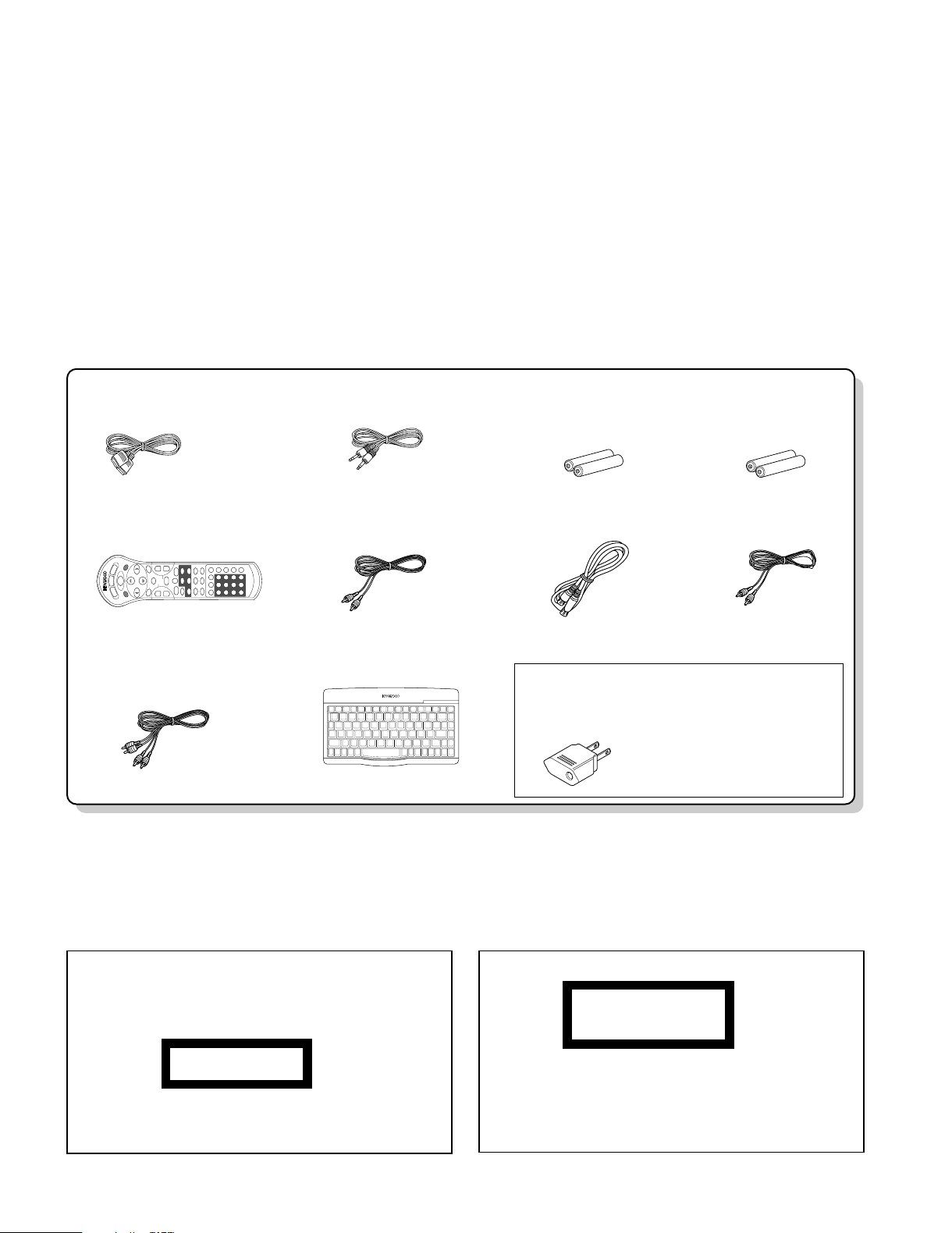
Standard remote
control unit (1)
Keyboard remote control unit(1)
REMOTE CONTROL UNIT RC-KB2
Audio cable
DV-5900M.............................(3)
DV-5050M/DVF-6050............(1)
(E30-0505-05)
Video cable(1)
(E30-1427-05)
RS-232C cable(1)
(E30-7209-05)
System control cable(2)
(E30-2816-05)
S-Video cable(1)
(E30-2956-05)
Coaxial cable(1)
(E30-2365-05)
DV-5900M only
Batteries (R03/AAA)(2)
Batteries (R6/AA)(2)
(DV-5900M only)
(A70-1486-05): RC-D0512.....KYEM
(A70-1488-15): RC-D0513.....K1
(A70-1513-05): RC-KB3.....K1
Battery cover (A09-1176-08)
Battery cover (A09-1242-08)
AC Plug Adaptor (1)
(E03-0115-05)
Use to adapt the plug on the
power cord to the shape of the
wall outlet.
(Accessory only for regions where
use is necessary.)
For countries other than U.S.A., U.S.-Military,
DV-5050M/5900M/DVF-J6050/J6050-G
CLASS 1
LASER PRODUCT
The marking of products using lasers
(For countries other than U.S.A., U.S.-
Military and Canada)
The marking this product has been classified as Class 1.
It means that there is no danger of hazardous radiation
outside the product.
CAUTION
VISIBLE LASER RADIATION
WHEN OPEN. DO NOT
STARE INTO BEAM.
Location: Back panel
Inside this laser product, a laser diode classified as Class
2 laser radiation is contained as alerted by the internal
caution label shown above. Do not stare into beam.
Location: DVD laser pick-up unit covproduct.
CONTENTS / ACCESSORIES / CAUTIONS
Contents
CONTENTS / ACCESSORIES / CAUTIONS............. 2
BLOCK DIAGRAM ......................................................3
CIRCUIT DESCRIPTION ............................................4
ADJUSTMENT ............................................................7
WIRING DIAGRAM ...................................................10
Accessories
PC BOARD ...............................................................11
SCHEMATIC DIAGRAM .......................................... 23
EXPLODED VIEW ....................................................61
PARTS LIST..............................................................64
SPECIFICATIONS ....................................................77
Cautions
2
DAT0-3
VIDEO ENCODER
PROGRESSIVE SCAN CONVERTER
MP3 DECODER
TRACKING
FOCUS
STD0-7
STD0-7
VD0-7
IEC OUT
B/Cb OUT 0-9
R/Cr OUT0-9
G/Y OUT0-9
Y, C
R, G, B
Y, Cb, Cr
Y
COMP
C
AV1 RGB OUT
DVD RGB
AV2 RGB
DVD Y, C, COMP
AV1 Y, C, COMP
AV2 Y, C, COMP OUT
AV2 Y, C, COMP
AV1 Y, C, COMP OUT
AV2 AUDIO
DVD AUDIO
AV1 AUDIO OUT
AV1 AUDIO
AV2 AUDIO OUT
AV2 FUNC,BLK
AV1 FUNC,BLK
AUDIO DAC
DRIVE
AUDIO SW
I/P SW
SCART CONTROL
VIDEO SW CONTROL
DMIX
AUT0 (FL, FR)
AOUT1 (SL, SR)
AOUT2 (C, SW)
Fs OUT
27M
SCAN CONVERTER
PROGRESSIVE
VIEDEO ENCODER
ODCADSC
MP3
CPPM,
DRIVE
DAC
IEEE1394
POWER
: AC230V~ 50Hz(E)
: AC110-120V
: AC120V 60Hz
50/60Hz
(K)
(Y)
A+9V/-9V
M+9V
AGND
FL-35V
FL+-
DGND/SGND
D+5V/3.3V
EV+12V
EVGND
EV+5V
DAC+5V
A+7V/-7V
A+5V/-5V
D+2.5V
PLAY/OPEN/CLOSE
CONTROL
/MGND
AUDIO
DVD
CD
/220-240V~
PROG
Y
C
13.5M
384Fs
768Fs
Y, Cb, Cr/
MP3 DATA , LRCK, BCK
AOUT,BCK,LRCK
Y, Cb, Cr
RGB
EX, Y, Cb, Cr
EX Y
EX C
DVD Y,C,COMPOSITE.RGB
EX VIDEO
EX SW CONTROL
+
VD0-7
ITU-R656
Y, C, Cb, Cr
R, G, B
Y, Cb, Cr/
PROGL
Y, Cb, Cr
Cr, Cb
DV-5900M USED ONLY
AUDIO
DAC
768Fs
384Fs
13.5M
ODC
ADSC
16.9344MHz
VIDEO
27M
33.8688MHz
512Fs
ENCODER
27MHz
VIDEO ENCODER
PICKUP UNIT
(X14-735)
MECHA.
(X00-3060-10)
CLK SYSTEM : DV-5900M
(X35-230) : DV-5050M/DVF-J6050 (X25-645) : DV-5050M/DVF-J6050
DV-5900M
DVF-J6050 ONLY
(X13-787)
(X13-787)
DV-5050M/DVF-J6050
DV-5900M ONLY
DV-5900M ONLY
DV-5900M ONLY
(X35-229) : DV-5900M (X25-644) : DV-5900M
DV-5900M ONLY
DVF-J6050 ONLY
DV-5050M ONLY
(K,Y) TYPE ONLY
CLK SYSTEM : DV-5050M/DVF-J6050
DV-5900M
ONLY
DV-5900M ONLY
ONLY
DV-5900M
DV-5900M ONLY
ONLY
DV-5050M/
DV-5900M
DVF-J6050
ONLY
DV-5050M/
ONLY
DVF-J6050
ONLY
DVF-J6050
DV-5050M/
PLL/DSL
HF
SERVO CONT
CIRC/DAC
SERVO CONTROLLER
MN67706
ADVANCED DISC OPTICAL DISC
CONTROLLER
ATAPI
ROM DEC
ECC
4MDRAM
MN103S13B
IC101
IC900 & SPREM
MP3 DECODER
DECODER
CPPM
IC400
MN5C027D4H
CSS2
DISSCRAMBLE
8M FLASH ROM
IC901
CSS DISSCRAMBLE
AV DECODER
VIDEO DECODER
MPEG,SUB PICTURE
AC3,LPCM,MP3
AUDIO DECODER
ENCODER
NTSC/PAL
PCM &
SPDIF
VIDEO DAC
SDRAM I/F
OSD
64M SDRAM
X35-230 (IC401)
ADDRESS DATA BUS
MP3 SW
DVD u-COM
IC201
8M FLASH ROM
IC207
8M FLASH ROM
IC215 IC500
DETECTOR
WATER MARK
MN7F015
EEPROM
IC206
S/P
APC
RF AMP
DRIVER
AN8499
MM
TRAVERSE/
LOADING SPDL
PICKUP
AN8708
AN8708
FRONT-END
PROCESSOR
COLOR, NR CONTROL
BRIGHT, SHARP, GANMA
PROGRESSIVE SCAN
CONVERTER
CGMS, MCROVISION
PROGRESSIVE SCAN CONVERTER
IC700
16M SDRAM
IC702
16M SDRAM
IC701
FL12200
VIDEO
DAC
ADV7196
IC800
YUV TO RGB MATRIX
COLOR, NR CONTROL
BRIGHT, SHARP, GANMA
VIDEO ENCODER
IC600
CAPTION CONTROL
CGMS, MCROVISION
3ch
6ch
DAC
VIDEO
ADV7190
13.5M
6.75M
6.75M
6.75M
MM1540
IC402
MUTE
ONLY
I/P SW
Y OUT
J6
Cb OUT
Cr OUT
J4
OUT
COMPOSIT
J5
J S1
S OUT
J S1/S2
S OUT
VIDEO FILTER & BUFFER
BLK. FUNC
IC451
SCART AV1
SCART AV2
S2
PROGL SW
IC1
SYSTEM u-COM
UPD784217
M
STOCKER
LOADING
M
DATA SW
FRONT
PCM1602KY
6ch DAC
IC205
192k 24bit
FOR FL, FR
FOR SL, SR
96k 24bit
FOR C, SW
96k 24bit
PCM1748
FOR DMIX
X25-645 (IC203)
2ch DAC
96k 24bit
60kHz
DMIX OUT SW
60kHz
60kHz
60kHz
LPF SW 110kHz
Q1-4
MUTE
(E) TYPE
Q5-8
MUTE
Q9-12
MUTE
Q13-16
MUTE
J1
MIX L
MIX R
FR
FL
SR
SL
SW
C
COAX.
J7
A1
OPT.
MP3
(IC900) 27MHz
(IC210)
1/2
X35
PLL
1/2
16.9344MHz
33.8688MHz
X25 (X302)
X25 (X301)
36.864MHz
Fs SW
1/2
SW
MP3
MP3
SW
1/2
DVD u-COM
X35 (IC201)
SW POWER SUPPLY
REG
X25-645 (Q201-204)
REG
X25-644 (Q202,204)
X35-229 (IC303)
REG
X25-645 (IC201)
REG
IR KEY
u-COM
IC2
LED
ED1(16-BT-90GNK)
FL
J12
J13
IC212,213
SW
MAIN DATA LINE
AUDIO LINE
VIDEO LINE
(IC209)
X25
OUT
OUT
COMPOSIT
OUT
AVDEC
SCART CONTROL
IC1
320DA150PGE
Y SW
C SW
S IN
J3
Cr IN
Cb IN
Y IN
MM1501
BH7635S
210
Q209,
AUDIO
AUDIO
IN L
IN R
EX SW
X25-644 (Q224)
J2
COAX.
IN
X25-645 (IC301)
EX SW
EEPROM
IC3
TEXT u-COM
EEPROM
IC4
UPD703034
IC2MAX232
IC13
IC12
HA12187FP
PC LINK
J10
DAISY
CHAIN
J8
IR TEXT
J9
M/S SW
S1
SRAM
IC14
2M
BACK UP
STOCKER LED
M
CLAMP
DOOR
M
IR
REMOCON
DOT DRIVER
IC1
JOG
S10
IC9
IC10
IC8
IC7
UPD78023GC
X35 (X201)
X35 (IC300)
X35 (IC211)
X25 (IC221)
X35-229 (IC301)
X35-229 (IC300)
X35-230 (IC301)
X25-644 (Q201,203)
X25-644 (IC218)
X25-645 (IC502,503)
X35-230 (IC601)
X35
X25-645 (IC211)
X25-644 (IC204)
CGMS, MCROVISION
YUV TO RGB MATRIX
COLOR, NR CONTROL
CAPTION CONTROL
ADV7170
4ch
VIDEO
DAC
BRIGHT, SHARP, GANMA
VIDEO ENCODER
IC600
DAC
VIDEO
3ch
PM0026A
I/P CONVERT
MCROVISION
PROGRESSIVE CONVERTER
IC601
(IC217)
1/2
1/2
X35 (IC201)
27MHz
X35 (IC211)
X35 (X202)
X35
(IC210)
AVDEC
PLL
(IC301)
DVD u-COM
X35
X35 (IC213)
X35
MIX R
MIX L
J1
AUDIO
IN R
AUDIO
IN L
X25-644 (IC215)
MPEG,DTS,AC3,LPCM
AUDIO DECODER
X35-230 : MN677533MP
X35-229 : MN677521HB
MIX L
MIX R
3M8703AV
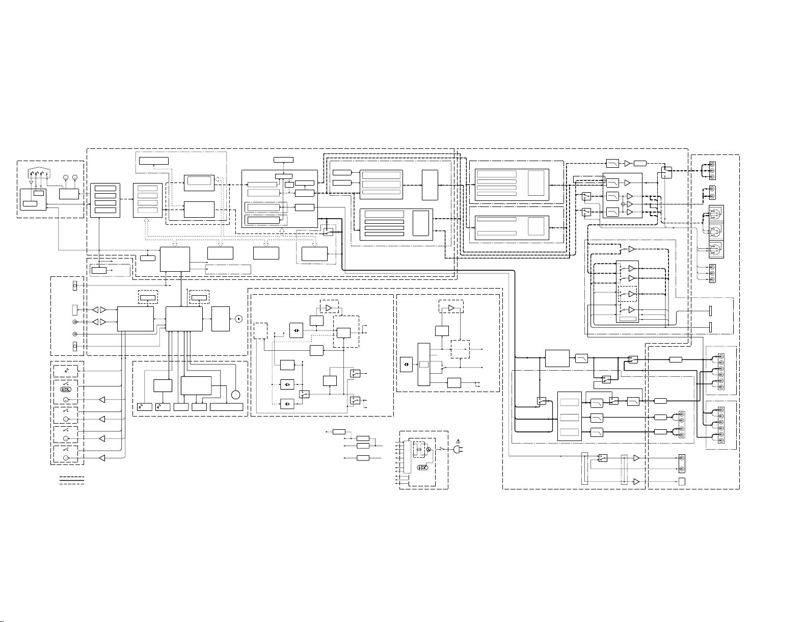
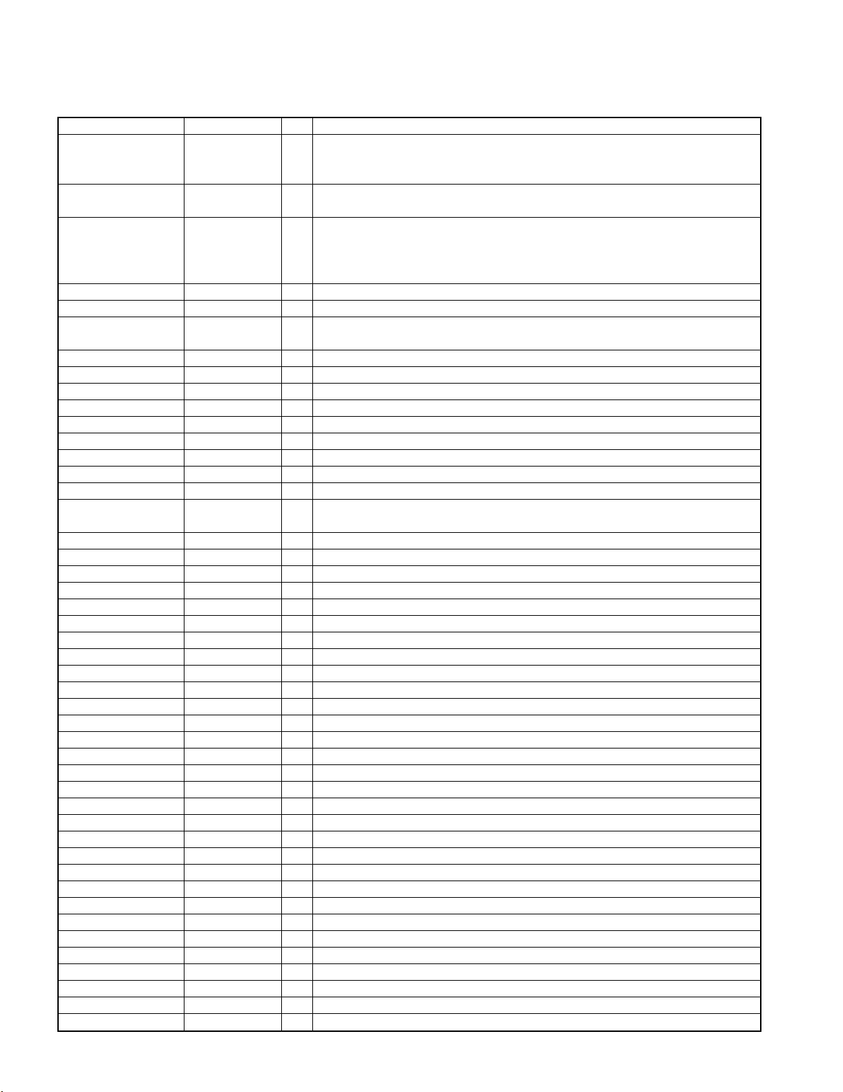
BLOCK DIAGRAM
DV-5050M/5900M/DVF-J6050/J6050-G
3
DV-5050M/5900M/DVF-J6050/J6050-G
CIRCUIT DESCRIPTION
1. Initializing
1-1 Initialization Method
• While holding down the "LIBRARY" key depressed,
plug the power cord into the socket.
POWER ON
óí"INITIALIZE"
The rotary tray turns.
ó
The rotary tray stops at disc 1 position.
ó
The microcomputer is initialized.
2. Test Mode
• This model has 3 kind of test modes : unit inspection,
factory test mode, measurement.
• In this manual, items of repair, test mode and inspection are available.
2-1 Setting Method
2-1-1 FCT Mode (Factory Mode)
• While holding down the MUSIC TYPE key depressed,
plug the power cord into the socket.
2-1-2 Inspection Mode
• While holding down the TEXT DISPLAY key
depressed, plug the power cord into the socket.
2-2 Cancellation of the Test Mode
• Unplug the power cord from the power socket.
2-3 Key Operation During the Test Mode
• During the test mode, it can be operated in a special
manner that is different from an ordinary operation by
using the keys on the panel, specifically as shown in
the following table.
FCT Mode
Key Mode Display Operation
PLAY - Playback time Disc playback
All segments light î
TEXT DISPLAY - Niagara mode î Display shows cyclically by pressing key.
Playback time î
SKIP UP Playback Playback time Playback next chapter/track #/program #
SKIP DOWN Playback Playback time Playback before chapter/track #/program #
STOP - Playback time Stop to operate and return to first step of this test mode.
RANDOM Playback Mute ON îMute OFF Mute works cyclically on or off.
USER FILE -
TIME DISPLAY -
DISC FLIP - OK or *** ERROR Self check mode (Refer to Servo Error Code)
PLUS1 PLAY - S-CW The stocker motor turns clockwise.
PLUS1 EJECT - S-CCW The stocker motor turns counterclockwise.
PLUS2 PLAY - OPEN The door opens.
PLUS2 EJECT - CLOSE The door closes.
PLUS3 PLAY - 0°î180° 0°î180°operation of clamper motor.
PLUS3 EJECT - 180°î0° 180°î0°operation of clamper motor.
OPEN/CLOSE - UNLOAD Unload operation of loading motor.
EJECT - LOAD Load operation of loading motor.
WIDE1îWIDE2
NORMAL
SCART RGB îSCART Video signal of SCART changes cyclically
YC SCART Through RGB(DVD)îY/C(DVD)îThrough(AV1 AV2)
WIDE mode changes cyclically WIDE1 or WIDE2.
INSPECTION Mode
Key Mode Display Operation
PLAY - Playback time Disc playback
SKIP UP Playback Playback time Playback next chapter/track #/program #
SKIP DOWN Playback Playback time Playback before chapter/track #/program #
STOP Playback INSPECTION Stop to operate and return to first step of this test mode.
Model/destination/
STOP Stop region code/u-com Display shows cyclically by pressing key.
version
RANDOM Playback Jitter ***% Shows jitter value(binary value vs time deviation of PLL-clock)
DISC FLIP -
MUSIC TYPE - CPPM KEY ID 13 figures. (DVD audio model only)
USER FILE - Playback time Indicated DISC No.400 in LCD remote controller.
4
180°SW OK(0°î180°)
0°SW OK(180°î0°)
Inverted inversion unit ASSY 0° to 180° or 180° to 0°.
DV-5050M/5900M/DVF-J6050/J6050-G
DEFINITION CONTENTS CODE BLOCK TIMING
ODC(Optical Device Control)
MOD_NOT_CRCOK No CRCOK signal 0x4303 (ADSC,ODC,disc ,pickup) Read address error at lead in or focus jump.
MAS_ECC_ERR Abnormal ODC
ODC
ERROR
ODC No emission OK on disc and host in 5 secs.
LAYER_CMP_ERR Abnormal LAYER in seek mode -
OUT_PB_AREA_NG OUT of PB AREA DATA_TR_PLAY_NG DATA Track Play SEEK_NG_CHGNV No data caused seek error -
UNCORRECT_ERR
No control data by demodulator
error
-
INVALID_CMD_ERR Out of secter ID 0xD601
Over data from disc(DVD:0xFFF)(VCD:
00:02:00 less)(CD:0xFFF)
UNCORRECT_LEADIN
No lead-in data by demodulator
error
0xD602 Time over in lead-in.
UNCORRECT_
KEYDET
No lead-in data by demodulator
error
0xD603
(ADSC,ODC,disc ,pickup)
ODC,disc
3. ERROR CODE OF CIRCUIT BY SELF CHECK MODE (TEST MODE)
DEFINITION CONTENTS CODE BLOCK TIMING
SERVO
TRAY_LOADING_ERR
Tray Loading Error. 0x4000
DCM_TRAYCTL_T(time out 5secs)
FOCUS_SVERR Focus Servo Error. 0x4100
SPINDLE_SVERR Spindle Servo Error. 0x4101
ADSC, Driver LSI, disc
Motor
DCM_DMON_T(time out 10
secs),Time out of checking
stop,Time out of start to turn.
DSC_DM_ERR
0x4102
ADSC, Driver LSI, disc
Motor
DCM_DMOF_T(time out 10secs),
DCM_DMMODE_T(time
out100ms) Abnormal turn of
disc motor.,
CDC_CLV_ERR
0x4103
ADSC, Driver LSI, disc
Motor
DCM_DMOF_T(time out 10secs)
Setting abnormal CLV
TRAVERSE_ERR Traverse Motor Error. 0x4104
DCM_INNER_T(time out 5secs)
TRACK_SVERR Tracking Servo Error 0x4105
DCM_TRON_T(time out 1sec)
Command error,Focus jump
Lock NG (ReSartServo) NG of
SEEK_TIMEOUT_ERR Seek Time Out Error 0x4106
Over 200 seek times
DSC_ERROR
ADSC
ERROR
ADSC
ERROR
ADSC
ERROR
ADSC
ERROR
ADSC
ERROR
ADSC Command error
DSC_NOTREADY
DSC Not Ready Error
ADSC ADSC REDY time out
DSC_TIM_ERR DSC TimeOut Error. ADSC
Over of CLV OK Over
of command end
DSC_COM_ERR
ADSC No use
DSC_ATN_ERR DSC Attention Error. ADSC
Error of CD-trick play and CD/DVD
seek. FC jump in DVD-play.
INVALID_MDTYP Out of Media 0x4300 ADSC
No check of media, Error after
servo retry. Abnormal disc.
DONOT_QREAD_ERR
0x4302 ADSC
Read error in Cue or
Rev play of CD
DSC_ESCAPE DSC Command Escape - ADSC
Stop servo operation after setting
the ESC flug in mode register of
ADSC.
FEP_IC_ERR
FEP
ERROR
ADSC ,FEP
jitter and data slice offset
adjustment error
FEP
CIRCUIT DESCRIPTION
DSC Disc Motor Error.
Abnormal FG-period in
DVD, Abnormal turn of
disc motor,
6626 CLVS Failure.
Abnormal FG-period in
CD
DSC Error
(status data error)
DSC Communication
Failure.
6626 QCODE do not
Read Error.
Adjustment error on data
slice offset
ADSC, TRAY
Mechanism, Motor LSI
ADSC, pickup &
actuator, Driver LSI
ADSC, Driver LSI, feed
Motor
ADSC, pickup &
actuator, Driver LSI
ADSC, pickup &
actuator, Driver LSI
DCM_FCON_T(time out 5secs),
Lock NG, NG of seek.
5
DV-5050M/5900M/DVF-J6050/J6050-G
DEFINITION CONTENTS CODE BLOCK TIMING
DISC
1. No CD-ROM Volume Descriptor
Set, No Primary Volume Descriptor
2. No Beginning Extended Area
Descriptor
3. No NSR Descriptor of "NSR02"
4. Length error of Main Volume
Descriptor Sequence
5. Directry of length error on
VIDEO_TS/AUDIO_TS after root
DISERR_TT_SRP_NO TT_SRP=0 0x2111 Disc format
ISERR_TT_SRP_OVER Value >TT_SRP 0x2112
DISERR_TT_SRP_MISS
0x2113
DISERR_TT_SRP_
PTT_OVER
Value >TT_SRP.PTT_Ns 0x2114
DISERR_TTU_SRP_NO TTU_SRP=0
0x2120 Disc format
DISERR_TTU_SRP_OVER Value >TTU_SRP 0x2121 Disc code
DISERR_PGCI_SRP_NO
PGCI_SRP=0 0x2131
Disc format
DISERR_PGCI_SRP_OVER Value>PGCI_SRP 0x2132
DISERR_TMAP_
SRP_OVER
Value>TMAP_SRP 0x2141
DISERR_TMAP_SA_NO TMAP_SA=0 0x2142
DISERR_TMAP_EN_NO MAP_EN=0
0x2143
DISERR_PGC_PGMAP_NO
C_POSIT is OK,
No PGMAP in PGC
0x2150
DISERR_PGC_PG_NO
C_POSIT is OK, PG=0 in PGC. 0x2151
DISERR_PGC_PG_OVER Value >PG in PGC 0x2152 Disc code
DISERR_PGC_C_PBIT_NO
C_POSIT is OK,
No C_PBIT in PGC
0x2153
DISERR_PGC_C_NO C_POSITis OK, Cell=0 in PGC 0x2154
DISERR_PGC_CN_NO Cell=0 0x2155
DISERR_PGC_C_OVER Value >Cell in PGC 0x2156 Disc code
DISERR_PGC_BLK_NO Block Cell only 0x2157
DISERR_SEARCH_CN_NO
No Cell# in search.
0x2160
Disc format
Disc code
UDF Bridge NG 0x2100
Disc code
Disc format
Disc format
CIRCUIT DESCRIPTION
DISERR_UDF
SRP is not meet with VTSN or
VTS_TTN
6
Disc format
DV-5050M/5900M/DVF-J6050/J6050-G
X25, IC2 X25, IC1 X35, IC201
STB MAIN IN 71 STB SUB SCK0 67 SCLK
STB MAIN 46 STB SUB IN SI 0 65 SBO (DVD u-Com)
uPD703034AGFA01 SO0 66 SBI
(Sub u-Com) SCK0 70 SCK 1
SI 0 69 SO 1
SO0 68 SI 1 LED(POWER) 23 LED (POWER)
LED PURE 24 LED PURE AUDIO
POWER IN 29 SUB WAKE LED 192K 25 LED 192kfs
LED 96K 26 LED 96kfs
LED DVD 62 LED DVD
X14, IC1
uPD780232GC012
75 SCK0 LINE2 34
(Dot Driver)
SO
CLK
73 SI 0 LINE3 63 D TERMINAL CONT.
SI
74 SO0 PLUGCH 56
STB
72 STB
RESET 23
RESET INPUT
POWER 28
POWER ON (PERIPHERY IC)
IC RESET 27
RESET (PERIPHERY IC)
uPD784217AGF519
TV
35 WIDE1 EXSW 30
VIDEO • AUDIO (INT.)/(EXT.) SW
MODE
35 WIDE2 VMUTE 31 VIDEO MUTE
CONT.
PURE AUDIO 32
VIDEO SW
K/J/E 53 DESTINATION YC L 33 CONTRAST MUTE
DV-5900M/5050M
MAIN/SUB1/2 SELECTION SW
54 MODEL DISCRIMINATION
55 M/S SW
X14, IC2
JOG 59 JOG 1 14~21
uPD17215GT-737
60 JOG 2 (D7~D0) D0~D7
REMOTE
X25, IC3 CONTROLLER
BR24C01AF RWRREQ 11 RWRREQ u-Com
SCL RTREN 13 RTREN
(EEPROM) SDA RWR 12 RWR
DPF-J6050 ONLY
X25, IC14
X25, IC451
84~91
(AD0~AD7)
BH7635S
76~83,92~99
BS62LV2000STC
(AUDIO/VIDEO SCL 3 SCL 1, 2
SW) SDA 4 SDA (A0~A17) (SRAM)
REMOTE 44 REM RD 5 OE
CONT. INPUT 45 REM RCV WR 6 WE
PLAY KEY 47 PLAY CS 7 CS
OPEN/CLOSE KEY 48 OPEN/CLOSE
POWER KEY 49 POWER ON
CIRCUIT DESCRIPTION
4. Main Microcomputer: uPD784217AGF519(X25, IC1)
4-1 Microcomputer Periphery Block Diagram
Key Matrix The number inside ( ) is pin number of FL driver & display u-com (X14, IC1).
0 DVD VIDEO STOP PAUSE PLUS1 PLAY
0.76~0.913 DVD AUDIO SKIP DOW EJECT PLUS1 EJECT
1.53~1.81 CD SKIP UP DISC FLIP PLUS2 PLAY
Key0(Pin22) Key1(Pin21) Key2(Pin20) Key3(Pin19)
2.32~2.71 MUSIC TAPE LIBRARY - PLUS2 EJECT
3.12~3.57 USER FILE TEXT DISPLAY - PLUS3 PLAY
3.93~4.41 SET - PLUS3 EJECT
7
DV-5050M/5900M/DVF-J6050/J6050-G
CIRCUIT DESCRIPTION
4-2 Port Function of Main Microcomputer
Port No. Port Name I/O Function
1 A16 O Address bus of SRAM (X25, IC14).
2 A17 O Address bus of SRAM.
3 SCL O Clock output for audio/video switching IC.
4 SDA I/O Data input/output for audio/video switching IC.
5 RD O Read strobe for SRAM (X25, IC14).
6 WR O Write strobe for SRAM (X25, IC14).
7 CS O Chip selector for SRAM (X25, IC14).
8 ASTB - Unused.
9 VDD - Supply voltage (+5V).
10 RGB H O RGB signal output. DVF-J6050 (E/T) Only
11 RWRREQ O Request of transmission data to remote cont. microcomputer.
12 RWR I Read-out the data of remote cont. microcomputer.
13 RTREN I Permission of transmission data from remote cont. microcomputer.
14~21 D7~D0 O Data output to remote cont. microcomputer (X14, IC2).
22 VPP - Unused.
23 STB LED O Control port for power led. ON
24 PURE LED O Control port for pure audio led. ON
25 192k LED O Control port for 192kfs led. ON
26 96k LED O Control port for 96kfs led. ON
27 ICRESET O Reset signal output to display microcomputer (X14, IC1). RESET
28 POWER O Power on/off control for regulator (X00, IC3). ON
29 SUB WAKE O Output port of power on signal to sub microcomputer.
30 EXSW O Switching port of (ext./int.) for video and audio output. INT.
31 VMUTE O Video mute control port. MUTE
32 PURE AUDIO
33 YC L O YC signal output. DVF-J6050 (E/T) Only OUT
34 LINE2 - Unused.
35 WIDE1 - Unused.
36 WIDE2 - Unused.
37 VDD - Supply voltage (+5V).
38 X2 - System clock input.
39 X1 I System clock input.
40 VSS - Connected to GND.
41 XT2 - Unused.
42 XT1 - Unused.
43 RESET I Reset signal input.
44 REM I Remote control signal input.
45 REM RCV I IR signal input.
46 STB SUB IN I Strobe signal input from sub microcomputer.
47 PLAY I Key input (PLAY) port. ON
48 OPEN/CLOSE I Key input (OPEN/CLOSE) port. ON
49 POWER ON I Input port of power on signal from sub microcomputer.
50 NC - Unused.
51 AVDD - Supply voltage (+5V).
52 AVREFO - Connected to VDD.
53 SHIMUKE I Discrimination of destination. K : 0V E : 5V
54 KISYU I Discrimination of model. DV-5050M : 5V DV-5900M : 2.5V
55 M/S SW I Input port of M/S switch. MAIN : 5V SUB1 : 2.5V SUB2 : 0V
56 PLUGCH - Unused.
57, 58 NC - Unused.
59 JOG1 I Encoder signal input.
60 JOG2 I Encoder signal input.
- Unused. DV-5050M/DVF-J6050 -
O Pure audio on/off control port. DV-5900M ON
Active
HL
8
DV-5050M/5900M/DVF-J6050/J6050-G
CIRCUIT DESCRIPTION
Port No. Port Name I/O Function
61 AVSS - Connected to GND.
62 LED DVD O DVD active led control port.
63 LINE3 - Unused.
64 AVREF1 - Connected to VDD.
65 SI0 I Data input from DVD microcomputer.
66 SO0 O Data output to DVD microcomputer.
67 SCK0 I Clock input from DVD microcomputer.
68 SI1 I Data input from sub microcomputer.
69 SO1 O Data output to sub microcomputer.
70 SCK1 I/O Clock input/output between main/sub microcomputer.
71 STB SUB O Strobe signal output to sub microcomputer.
72 STB O Strobe signal output to display microcomputer (X14, IC).
73 SI I Data input from display microcomputer (X14, IC).
74 SO O Data output to display microcomputer (X14, IC).
75 SCK0 O Clock output to display microcomputer (X14, IC).
76~83 A0~A7 O Address bus of SRAM (X25, IC14).
84~91 AD0~AD7 I/O Data bus of SRAM (X25, IC14).
92~99 A8~A15 O Address bus of SRAM (X25, IC14).
100 VSS - Connected to GND.
5. Sub Microcomputer: 703034AGFA01(X25-644/655, IC2)
5-1 Sub Microcomputer Periphery Block Diagram
X25, IC1
Active
HL
Main Microcomputer
uPD784217AGF519
S.DT 98
SCX0 99
DVM-01
STCKER MOTOR + 56 R CCW
STCKER MOTOR - 55 R CW
DOOR MOTOR + 51 DOOR CLOSE
DOOR MOTOR - 52 DOOR OPEN
CLUMP MOTOR + 53 CLUMP -
CLUMP MOTOR - 54 CLUMP +
LOADING MOTOR + 57 UNLOAD X25, IC13
LOADING MOTOR - 60 LOAD
D 1 91 PWM IERX 26 Daisy Chain
Q 1 68 D SW Drive IC
PH 1 70 PH 1 IETX 27 HA12187FP
PH 3 71 PH 3
PH 2 72 PH 2 Microcomputer
S1 77 LOCK SW X25, IC12
S2 78 CLOSE SW
D2 89 EJECT LED DSR 4 DSR
S3 61 OPEN SW DTR 5 DTR
S4 63 EJECT SW RXD 1 6 TD
S5 64 0 SW TXD 1 7 RD
S6 66 180 SW
S7 67 90 SW
S9 79 PL SW
S8 80 HP SW
S LED 92 S LED
Sub
4 DSR
S.RQ 95
M.DT 97
5 DRT
6 RXD1
M.RQ 96
MAX232NS
PC Drive IC
7 TXD1
X25(IC12)
DSR
DTR
PC Drive IC
MAX232NS
RD
TD
9
DV-5050M/5900M/DVF-J6050/J6050-G
CIRCUIT DESCRIPTION
5-2 Port Function of Sub Microcomputer
Port No. Port Name I/O Function
1 TXD0 - No used.
2,3 NC - No used.
4 DSR O PC link data set ready output. READY
5 DTR I PC link data set ready input.
6 TD I PC link data input.
7 RD O PC link data output.
8 NC - No used.
9 EVDD - Supply voltage.
10 EVSS - GND
11~20 NC - No used.
21 IC/VPP - Connected to VSS.
22~25 NC - No used.
26 IERX I Daisy chain IE bus data input.
27 IETX O Daisy chain IE bus data output.
28~33 NC - No used.
34 RESET I Reset signal input.
35 NC - GND
36 NC - No used.
37 REGC - No used.
38 X2 - Crystal resonator connection.
39 X1 I Crystal resonator connection.
40 VSS - GND
41 VDD - Supply voltage.
42 CLKOUT - No used.
43~48 NC - No used.
49 SCL O Clock output for ROM correction.
50 SDA I/O Data input/output for ROM correction.
51 DOOR CLOSE O Control port of door motor for mechanism. CLOSE
52 DOOR OPEN O Control port of door motor for mechanism. OPEN
53 CLUMP -M O Control port of clump motor for mechanism. 180°î0°
54 CLUMP-P O Control port of clump motor for mechanism. 0°î180°
55 R CW O Control port of rotary motor for mechanism. CW
56 R CCW O Control port of rotary motor for mechanism. CCW
57 UNLOAD O Control port of load motor for mechanism. UNLOAD
58 BVDD - Supply voltage.
59 BVSS - GND
60 LOAD-M O Control port of load motor for mechanism. LOAD
61 OPEN SW I Input port of open switch for mechanism. OPEN
62 NC - No used.
63 EJECT SW I Input port of eject switch for mechanism. EJECT
64 0 SW I 0°switch input of mecha, traverse. 0°
65 NC - No used.
66 180 SW I 180°switch input of mecha, traverse. 180°
67 90 SW I 90°switch input of mecha, traverse. 90°
68 D SW I Input port of disc sensor for mechanism.
69 NC - No used.
70 PH 1 I Detection port of stocker position.
71 PH 3 I Detection port of stocker position.
72 PH 2 I Detection port of stocker position.
73 NC - No used.
74 AVDD - Analog power supply.
75 AVSS - Connected to VSS.
76 AVREF - Reference voltage.
Active
HL
10
DV-5050M/5900M/DVF-J6050/J6050-G
CIRCUIT DESCRIPTION
Port No. Port Name I/O Function
77 LOCK SW I Input port of stocker lock switch for mechanism. LOCK
78 CLOSE SW I Input port of door close switch for mechanism. CLOSE
79 PL SW I Mechanism load clump position switch input.
80 HP SW I Mechanism home position switch input.
81~88 NC - No used.
89 EJECT LED O Control port of eject LED. LED ON
90 +B O On/off control port of power supply for photo sensor (PH 1~3). ON
91 PWM O Disc sensor on/off control. ON
92 S LED O Control port of LED in the stocker. LED ON
93 POWER OUT O Output port of power on signal to main microcomputer.
94 POWER IN I Input port of power on signal from main microcomputer.
95 SUB-STB I Request signal input from main microcomputer REQUEST
96 MAIN-STB O Request signal output to main microcomputer REQUEST
97 SI0 I Serial data input from main microcomputer.
98 SO0 O Serial data output to main microcomputer.
99 SCX0 I Serial clock input from main microcomputer.
100 RXD0 - No used.
Active
HL
6. Port Function of ICs
6-1 AV decoder : MN677521HB (X35, IC300)
• Port Function
Port No. Port Name I/O Function
1,9,32,46,53,73,104
116,142,156,160,166
172,179,184,191,197
205
2~4,6~8,10,201
203,204,206,207
5,14,27,42,52,60,70
83,92,105,120,147
157,163,169,176,182
186,194,200,208
11 CLK121 - Connected to digital ground.
12,37,66,79,96,112
145,174,188,202
13 XRST I System reset input. L : Reset
15 CLK81 - Connected to digital ground.
16 PLLAVDD - Main PLL supply voltage (+3.3v).
17 TCPOUT 0 Unused.
18 PLLAVSS - Connected to digital ground.
19 CLK27 I System clock input (27MHz).
20 PLLTEST I Test input port for main PLL. L : Fixed
21 CKIO I Decode clock change-over.
22 PLLVDD - Supply voltage (+2.5V) of internal logic for main PLL..
23,24 HMD1,HMD0 - Connected to digital supply voltage (+3.3V).
25 XHINT O Interruption to DVD microcomputer. L : Active
26 XDK O Acknowledgment to DVD microcomputer. L : Active
28 XWR I Write enable from DVD microcomputer.
29 XRD I Read enable from DVD microcomputer.
30 XCS I Chip select from DVD microcomputer.
31 HCLK I Clock input from DVD microcomputer.
33~36,38~41,43~45 HA1~HA11 I Address input from DVD microcomputer.
VDD - Digital supply voltage (+3.3V).
MA0~MA11 O SDRAM address 0~11
VSS - Digital ground.
LVDD - Digital supply voltage (+2.5V) for internal logic.
PLAY
POSITION
HOME
POSITION
11
DV-5050M/5900M/DVF-J6050/J6050-G
CIRCUIT DESCRIPTION
Port No. Port Name I/O Function
47~51,54~59,61~65 HD0~HD15 I/O DVD microcomputer data bus 0~15.
67 AUDSTR I Valid signal of bit stream input data.
68 ARQ 0 Unused.
69 VSTR I Clock signal input for bit stream.
71 VRQ O Request of program stream.
72 AVRTM I Sector separation signal.
74~78,80~82 STD0~STD7 I Bit stream parallel input 0~7.
84 EXTCK I External FS384 input terminal.
85 APLLVDD - Supply voltage (+2.5V) of internal logic for Audio PLL..
86 P5481 - Audio PLL ground.
87 PHCOPMO O Audio PLL phase comparison output.
88 APLLAVSS - Audio PLL ground.
89 NC - Unused.
90 APLLAVDD - Supply voltage (+3.3V) for Audio PLL..
91 ACKIO - Connected to digital ground.
92 VSS - Digital ground.
93 DCTEST - Connected to digital ground.
94,95 TESTSEL1,0 - Connected to digital ground.
97~102,106,108,109
103 CLKMON O Unused.
107 RFF O Unused.
110 IECOUT O IEC958 format data output.
111 DMIX O Audio down mix signal output.
113 DACCK O Over sampling DAC clock output
114 LRCK O LR clock output.
115 SRCK O Bit clock output.
117~119 ADOUT(0~2) O Audio data output (0~2).
121 XPOWD I DAC power down control input.
122 VREFC I DAC reference voltage input for C signal.
123 IREFC I DAC bias current setting port for C signal.
124 COMPC I Capacitance connection for DAC (C signal) stabilization.
125 VCOUT O Unused.
126,136 AVDD - Analog supply voltage (+3.3V) for DAC.
127 VREFCB I DAC reference voltage input for CB signal.
128 IREFCB I DAC bias current setting port for CB signal.
129 COMPCB I Capacitance connection for DAC (CB signal) stabilization.
130 VCBOUT O Unused.
131,141 AVSS - Analog ground for DAC.
132 VREFCR I DAC reference voltage input for CR signal.
133 IREFCR I DAC bias current setting port for CR signal.
134 COMPCR I Capacitance connection for DAC (CR signal) stabilization.
135 VCROUT O Unused.
137 VREFY I DAC reference voltage input for Y signal.
138 IREFY I DAC bias current setting port for Y signal.
139 COMPY I Capacitance connection for DAC (Y signal) stabilization.
140 VYOUT O Unused.
143 XYSYNCO I/O Vertical synchronizing signal input/output.
144 XHSYNCO I/O Horizontal synchronizing signal input/output.
146 VCLK O Clock output for digital video data output.
148~155 VD0~VD7 O Digital video data output (0~7).
158,159,161,162
164,165,167,168
170,171,173,175
177,178,180,181
TEST4~TEST9
TEST3,1,0
MDQ0~MDQ15 I/O SDRAM data bus (0~15).
O Unused.
12
DV-5050M/5900M/DVF-J6050/J6050-G
CIRCUIT DESCRIPTION
Port No. Port Name I/O Function
183 MCKI I Clock input from SDRAM.
185 MCK O Clock output to SDRAM.
187 DQMLE O Lower bite data, mask signal of expander SDRAM.
189 DQMLM O Lower bite data, mask signal of main SDRAM.
190 DQMUE O Upper bite data, mask signal of expander SDRAM.
192 DQMUM O Upper bite data, mask signal of main SDRAM.
193 XWE O Write enable signal of SDRAM.
195 XCAS O CAS signal of SDRAM.
196 XRAS O RAS signal of SDRAM.
198 XCSE O Chip select signal of expander SDARM.
199 XCSM O Chip select signal of main SDARM.
• Block Diagram
ODC, TS
Decoder etc.
System Controller
(Microprocessor)
SDRAM
(16bit)
Stream
Interface
Stream
Parser
Host
Interface
Memory
Interface
CD-DA
Video
and
Audio
Decoder
Sub- picture REC656
Decoder (Digital Video Out)
Video
Interface
NTSC/PAL
Encoder
Audio DAC
Interface
IEC958
PLL 27MHz
DAC
DAC
DAC Cr
Y/Y
Cb/Composite
C/C
Audio Out
(DAC for Audio)
13
DV-5050M/5900M/DVF-J6050/J6050-G
CIRCUIT DESCRIPTION
6-2 Port Function of AV decoder : MN677533MP (X35, IC301) DV-5050M/DVF-J6050 only
Port No. Port Name I/O Function
1,9,34,48,53,74,91,98,
111,156,160,166,172, VDD - Digital supply voltage (+3.3V).
179,184,191,197,205
2~4,6~8,10,201
203,204,206,207
5,19,24,29,44,52,58,
68,84,95,107,151,
157,163,169,176,182,
186,194,200,208
11,13,15~18,20~23 TEST0~TEST9 O Test terminal.
12 XRST I System reset input. L : Reset
14,39,63,79,87,105,
146,174,188,202
25 HMD1 I Select signal 1 from DVD microcomputer.
26 HMD0 I Select signal 0 from DVD microcomputer.
27 XHINT O Interruption to DVD microcomputer. L : Active
28 XDK O Acknowledgment to DVD microcomputer. L : Active
30 XWR I Write enable from DVD microcomputer.
31 XRD I Read enable from DVD microcomputer.
32 XCS I Chip select from DVD microcomputer.
33 HCLK I Clock input from DVD microcomputer.
35~38,40~43,45~47 HA1~HA11 I Address input from DVD microcomputer.
49~51,54~57
59~62,64~67,69
70 AUDSTR I Valid signal of bit stream input data.
71 VSTR I Clock signal input for bit stream.
72 VRQ O Request of program stream.
73 AVRTM I Sector separation signal.
75~78,80~83 STD0~STD7 I Bit stream parallel input 0~7.
85 IECOUT O IEC958 format data output.
86,92~94 ADOUT(0~3) O Audio data output (0~3).
88 DACCK O Over sampling DAC clock output.
89 LRCK O LR clock output.
90 SRCK O Bit clock output.
96 CLKMON O Clock output.
97 CLK121 I External clock (121.5MHz) input. (Unused)
99 CLK27 I System clock input (27MHz).
100 PLLAVDD - Main PLL supply voltage (+3.3V).
101 TCPOUT 0 Unused.
102 PLLAVSS - Connected to digital ground.
103 CKIO I Decode clock change-over.
104 PLLVDD - Supply voltage (+1.8V) of internal logic for main PLL.
106 CLK81 - Connected to digital ground.
108 APLLVDD - Supply voltage (+1.8V) of internal logic for Audio PLL.
109 ATCPOUT O Unused.
110 EXTCK I External FS384 input terminal.
112 APLLAVDD - Supply voltage (+3.3V) for Audio PLL.
113 ATVROUT O Unused.
114 AVCOIN - Connected to digital ground.
115 APLLAVSS - Connected to digital ground.
116 VREFB I DAC reference voltage input for C signal.
117 IREFB I DAC bias current setting port for C signal.
118 COMPB I Capacitance connection for DAC (C signal) stabilization.
119 VBOUT O C signal output for DAC.
MA0~MA11 O SDRAM address 0~11
VSS - Digital ground.
LVDD - Digital supply voltage (+1.8V) for internal logic.
HD0~HD15 I/O DVD microcomputer data bus 0~15.
14
DV-5050M/5900M/DVF-J6050/J6050-G
CIRCUIT DESCRIPTION
Port No. Port Name I/O Function
120,130 AVDD(1,0) - Analog supply voltage (+3.3V) for DAC.
121 VREFG I DAC reference voltage input for Cb signal.
122 IREFG I DAC bias current setting port for Cb signal.
123 COMPG I Capacitance connection for DAC (Cb signal) stabilization.
124 VGBOUT O Cb signal output for DAC.(Unused)
125,135 AVSS(0,1) - Analog ground for DAC.
126 VREFC I DAC reference voltage input for Cr, C signal.
127 IREFC I DAC bias current setting port for Cr, C signal.
128 COMPC I Capacitance connection for DAC (Cr, C signal) stabilization.
129 VCOUT O Unused.
131 VREFY I DAC reference voltage input for Y signal.
132 IREFY I DAC bias current setting port for Y signal.
133 COMPY I Capacitance connection for DAC (Y signal) stabilization.
134 VYOUT O Y signal output for DAC.
136 NC - Unused.
137 ACKIO - Connected to digital ground.
138 MODE121 I Connected to digital ground.
139 PLLTEST I Connected to digital ground.
140,141 TESTSEL1,0 - Test mode terminal. L : Fixed
142 DCTEST - DC test mode terminal.
143 XYSYNCO I/O Vertical synchronizing signal input/output.
144 XHSYNCO I/O Horizontal synchronizing signal input/output.
145 VCLK O Clock output for digital video data output.
147~150,152~155 VD0~VD7 O Digital video data output (0~7)
158,159,161,162,
164,165,167,168,
170,171,173,175,
177,178,180181
183 MCKI I Clock input from SDRAM.
185 MCK O Clock output to SDRAM.
187 DQMLE O Lower bite data, mask signal of expander SDRAM.
189 DQMLM O Lower bite data, mask signal of main SDRAM.
190 DQMUE O Upper bite data, mask signal of expander SDRAM.
192 DQMUM O Upper bite data, mask signal of main SDRAM.
193 XWE O Write enable signal of SDRAM.
195 XCAS O CAS signal of SDRAM.
196 XRAS O RAS signal of SDRAM.
198 XCSE O Chip select signal of expander SDARM.
199 XCSM O Chip select signal of main SDARM.
MDQ0~MDQ15 I/O SDRAM data bus (0~15).
15
DV-5050M/5900M/DVF-J6050/J6050-G
CIRCUIT DESCRIPTION
6-3 Port Function of DVD Microcomputer : MN102N62GGB (X35, IC201)
Port No. Port Name I/O Function
1 WAIT I Bus wait port.
2
3 NWEL 1:1 24MHz DV-5050M/DVF-J6050
4
5 RAMCS(SRAM) O SRAM chip select.
6 ODCCS O ODC chip select.
7 AVCS(AVDEC) O AV decoder chip select.
8 ROMCS(ROM) O Flash ROM chip select.
9 SCLOCK(VDAC) O
10 SDATA(VDAC) O
11 FRD(ROM) O Flash ROM read port.
12 WORD - Connected to VDD (+3.3V).
13~16 CPUADR0~3 O Bus address (0~3).
17 VDD - Supply voltage (+3.3V).
18 SYSCLK(AVDEC) O Clock output to AV decoder (X35, IC300).
19 VSS - Connected to GND.
20 XI I Connected to GND.
21 XO O Unused.
22 VDD - Supply voltage (+3.3V).
23 OSCI(CLK135) I System clock input (13.5MHz).
24 OSCO O Unused.
25 MODE I Processor mode selection.
26~33 CPUADR4~11 O Bus address (4~11).
34 AVDD - Supply voltage (+3.3V).
35~42 CPUADR12~19 O Bus address (12~19).
43 VSS - Connected to GND.
44 CPUADR20 O Bus address (20).
45 25BSY O Busy data output. Normal Busy
46 STBPSL O
47 HFMON O HF monitor output.
48 KMODE O Selection for writing the ROM. Writing Normal
49 AMUTE O Audio mute control.
50 CIRCEN(ENC) O Enable to Digital Servo Controller (X35, IC1).
51 PROGSW I
52 STBTI O
53 FRSW O Flash ROM 1, 2 (X35, IC207, 215) change-over. Default
54 VDD - Supply voltage (+3.3V).
55 FEPEN O Enable to FEP (traverse).
56 CLKSEL O Clock selection.
57 STBDAC2 O
58 STBSP1 O
NRD(ODC/AVDEC
/SRAM)
NWEH (ODC/AVDEC
/SRAM/ROM)
O Bus read port.
O Selection port of clock (2:1). 0:0 33MHz, 0:1 36MHz,
Unused. DV-5900M
O Bus read port.
Clock output to VDAC (IC600). DV-5050M/DVF-J6050
(X25, IC600) DV-5900M (X35, IC600)
Data output to VDAC (IC600). DV-5050M/DVF-J6050
(X25, IC600) DV-5900M (X35, IC600)
Strobe output to Progressive Convert DAC (X25, IC601). DV-5050M
Unused. DV-5900M/DVF-J6050
Unused. DV-5050M/DVF-J6050
Change-over the component terminal. DV-5900M
Unused. DV-5050M/DVF-J6050
Strobe output to MP3 decoder (X35, IC900). DV-5900M
Unused. DV-5050M/DVF-J6050
Strobe output to ADAC (X25, IC205). DV-5900M
Unused. DV-5050M/DVF-J6050
Strobe output to serial-parallel converter (X25, IC224). DV-5900M
Active
HL
Expan.
Mode
16
DV-5050M/5900M/DVF-J6050/J6050-G
CIRCUIT DESCRIPTION
Port No. Port Name I/O Function
59 STBDAC1 O
60 ADSCEN(ENS) O Enable to Digital Servo Controller (X35, IC1).
61 VSS - Connected to GND.
62 WMINT I
63 E2CS O Chip select to EEPROM (X33, IC206).
64 SCSIBN O Enable control to jig for writing the ROM.
65 196BSY I Busy data input. Normal Busy
66 VDD - Supply voltage (+3.3V).
67 SCLK0 O
68 SI0 I
69 SO0 O
70 SCLK1 O SIO1 clock output for control ICs.
71 SI1 I SIO1 data input for control ICs.
72 SO1 O SIO1 data output for control ICs.
73 PULL UP0 I Unused.
74 PULL UP1 I Unused.
75 NMI I Unused.
76 ADSCINT I Interruption port from Digital Servo Controller (X33, IC1).
77 ODCINT I Interruption port from Optical Disc Controller (X33, IC101).
78 AVINT I Interruption port from AV decoder (X33, IC301).
79 ICRST O Reset signal output to periphery ICs.
80 MP3INT I
81 ADSEP I Unused.
82 RST I Reset signal input.
83 VDD - Supply voltage (+3.3V).
84~91 CPUDT0~7 I/O Bus data (0~7) input and output.
92 VSS - Connected to GND.
93~100 CPUDT8~15 I/O Bus data (8~15) input and output.
Strobe output to ADAC. X25, IC204 (DV-5900M)
X25, IC203 (DV-5050M/DVF-J6050)
Unused. DV-5050M/DVF-J6050
Interruption port from Water Mark Detector (X35, IC500). DV-5900M
SIO0 clock output to communicate between main
microcomputer and DVD system microcomputer.
SIO0 data input to communicate between main
microcomputer and DVD system microcomputer.
SIO0 data output to communicate between main
microcomputer and DVD system microcomputer.
Unused. DV-5050M/DVF-J6050
Interruption port from MP3 decoder (X33, IC900). DV-5900M
Active
HL
17
DV-5050M/5900M/DVF-J6050/J6050-G
CIRCUIT DESCRIPTION
6-4 Digital Video Enhancer : FL12220 (X35, IC703) DV-5900M only
• Port Function
Port No. Port Name I/O Function
External OSD Interface
1~5 OSDC(0~4)
156~160 OSDC(5~9)
6 OSDSEL - External OSD select input. (Connected to ground.)
144~153 OSDY(0~9) - External OSD luma input. (Connected to ground.)
Test outputs(Not shown on Block diagram)
7~10 TEST(03~06)
13~15 TEST(00~02)
Test inputs(Not shown on Block diagram)
19 TESTB I Active low test input. This pin should be tied to VDD for normal operation.
69,70,143 TEST (0~2) I Active high test inputs. This pin should all be tied to VSS for normal operation.
Power Supply Connections(Not shown on Block diagram
11,28,40,49,59,60,81,
87,93,99,101,107,
113,119,121,127, supply and decouple to the digital ground plane.
131,135,141,154
12,29,41,50,79,80,82,
88,94,100,102,108,
114,120,122,128,
132,136,142,155
72 ISINK -
68 AVDD - Analog power connections for the clock PLL circuits.
74 AVDD - Analog power connections for the video DAC circuits.
Control Signals
16 SDA I I2C compatible serial control bus data.
17 SCL I/O I2C compatible serial control bus clock.
18,20 MODE(0,1) - I2C operating MODE( 0,1).
21~23 ADDR(0~2) -
24 I2CCLK I Clock input for the internal I2C circuit.
25 RESETB I
67 CLKIN I Master clock input.
139 ENHOFF - When this pin is set low the FL12220 will be in normal enhancement mode.
Input Signals
26,27,30~37 CBIN(0~9) I 10-bit non-multiplexed Cb or multiplexed Cb/ Cr signal input bus.
43~48,51~54 CRIN(0~9 I 10-bit non-multiplexed Cr signal input bus.
55~58,61~66 YIN(0~9) I 10bit luminance or multiplexed Y/Cb/Cr signal input bus.
Input Signals(cont.)
38 HBLANKI I Horizontal input blanking signal.
39 VBLANKI I Vertical input blanking signal.
42 FLDIN I Odd/Even field designator input.
Analog Output Signals
71 R/Cr-ANA O Analog output.
73 G/Y-ANA O Analog output.
75 B/Cb-ANA O Analog output.
76 COMP -
77 RSET - Current setting resistor for video DACs.
78 VREF - Voltage reference for video DACs.
VDD -
VSS - Digital ground connections. Connect to the digital ground plane.
I Multiplexed chroma signal is input on this bus. ( Connected to ground.)
O Test outputs. These pins should be left unconnected for normal operation.
Digital power connections. Connect to the digital +3.3 volt power
Analog current sink return for the video DAC circuits. Connect to the analog
ground plane.
The setting of ADDR(0~2) allow the I
programmed to prevent conflict with the other I2C devices in the system.
Reset. When this input is set low it will reset all internal registers
to the default states.
Compensation for video DACs. Should be connected to analog
groundvia a capacitor.
2
C address of the device to be
18
DV-5050M/5900M/DVF-J6050/J6050-G
CIRCUIT DESCRIPTION
Port No. Port Name I/O Function
Digital Output Signals
83~86,89~92
95,96
115~118,123~126
129,130
Digital Output Signals(cont.)
97,98,103~106
109~112
133 HBLANKO O Horizontal output blanking signal.
134 VBLANKO O Vertical output blanking signal.
137 YCLKO O Output luma sampling clock.
138 FLDO I Odd/Even field designator input.
140 CCLKO O Output chroma sampling clock.
• Simplified Block Diagram
HREFI
VREFI Sync & Timing Luma Triple
FLDIN Control Large- Edge 10-bit
CLKIN Enhancer DAC
30 Input YUV /RGB
Formatter Interpolator Color-Space
Digital Luma Converter
YUV/
Ycr Cb
G/YOUT(0~9) O Green or luminance output bus.
CBOUT(0~9) O Blue or Cb chrominance output bus.
CROUT(0~9) O Red or Cr chrominance output bus.
Detail
Enhancer
Line YUV YCrCb/
Memories
& Output
Formatter
Analog
30
Digital
RGB
SCL
SDA
2
C
I
Interface Registers
Control Chroma Decimator OSD
Large-Edge
Enhancer
(Optional)
Engine &
Interface
External
OSD
19
DV-5050M/5900M/DVF-J6050/J6050-G
CIRCUIT DESCRIPTION
6-5 Video Deinterlacer : FL12200(X35, IC700) DV-5900M only
• Port Function
Port No. Port Name I/O Function
Test outputs
112,113 TEST(00, 01) O These pins are test outputs and should be left unconnected in normal operation.
Test inputs
41,50,51,108 These pins are used for test purposes only and should always be tied low
109,111
Power Supply Connections(Not shown on Block diagram)
1,33,63,73,84,95
105,114,123,137 VDD33 -
144,151, 167
2,17,34,55,64,74
85 ,96,106,115
124,132, 138,145
152,159,168
43 AVSS - Ground connection for the clock PLL circuits. Connect to the digital ground plane.
16,54,107,158 AVDD25 -
42 AVDD -
Control Signals
49 RESETB I
53 OE O
56~58 IFORMAT(2~0) I Input signal format control.
59~61 OFORMAT(2~0) O Output signal format control.
44,45 DADDR(1,0) -
46 MODE -
47 SDA I 2-wire serial control bus data.
48 SCL I/O 2-wire serial control bus clock.
40 PIXCLK I Pixel clock input. This clock is used to drive all the circuits in the FL12200.
62 N/P/IN/OUT I/O NTSC/PAL input or output.
Control Signals(contd.)
52 NOMEM I No memory mode control input.
Input Signals
18~27 G/YIN(0~9) I 10-bit green or luminance signal input bus.
6~15 B/CbIN(0~9) I 10-bit blue or Cb chroma signal input bus.
28~32 R/CrIN(0~4)
35~39 R/CrIN(5~9)
3 HSYNCREFI I Horizontal sync or reference.
4 VSYNCREFI I Vertical sync or reference.
5 FIELDIN I Field identifier input.
Output Signals
65~72 G/YOUT(2~9)
75,76 G/YOUT0,1
93,94 B/CbOUT8,9
97~104 B/CbOUT(0~7)
77~83 R/CrOUT(3~9)
86~88 R/CrOUT(0~2)
116 CCLKO O Chroma output sampling clock.
117 YCLKO O Luma output sampling clock.
89 VREFO - Start of active field or frame indicator.
90 HREFO O Start of active line indicator output.
20
TEST(0~5) -
VSS - Ground connections. Connect to the digital ground plane.
for normal operation.
Pad Ring digital power connections. Connect to the digital +3.3 volt power
supply and decouple to the digital ground plane.
Core Logic digital power connections. Connect to the digital +2.5 volt
power supply and decouple to the digital ground plane.
Analog power connections for the clock PLL circuit. Connect to a separately
decoupled +2.5 volt power supply and decouple directly to the AVSS pin.
Reset. When this input is set low it will reset all the internal registers
to the default states.
When this pin is set high the the outputs of the FL12200 will be enabled ; when
it is set low the outputs will be set into a high-impedance state.
The settings of DADDR(1,0) allow the device address of the control bus to
be programmed to prevent conflict with the other devices connected to the bus.
When this pin is set low the control bus will operate in the slave mode; allowing
the device to programmed from an external controller.
I 10-bit red or Cr chroma signal input bus.
O Green or luminance output bus.
O Blue or Cb chrominance output bus.
O Red or Cr chrominance output bus.
DV-5050M/5900M/DVF-J6050/J6050-G
CIRCUIT DESCRIPTION
Port No. Port Name I/O Function
91 VSYNC/CREFO O
92 H/CSYNCO O
110 FILM O Film mode detector output.
SDRAM Interface Signals
125~131 ADDR(4~10) SDRAM address bus. This signal bus is used to address
133~136 ADDR(0~3)
139~143,146~150 DATA(0~4)
153~157,160~166 5~9,10~14, -
169~176 15~21,22~29
118 MEMCLKO O SDRAM clock and 2x output sampling clock.
119 WEN -
120 RASN -
121 CASN -
122 BSEL - SDRAM bank select.
Vertical sync output. This signal provides the vertical sync function
for the outputs.
Horizontal or composite sync output. This signal provides the horizontal sync
function for the outputs.
the external SDARM(s) used for field memories.
SDRAM data bus. This signal bus is used to transfer the data to and from
the external SDRAM(s) used for field memories.
SDRAM write enable. This active low signal should be connected
to the WE pin(s) on the SDRAM(s).
SDRAM row address select. This active low signal should be connected to
the RAS pin(s) on the SDRAM(s).
SDRAM column address select. This active low signal should be connected to
the CAS pin(s) on the SDRAM(s).
• Simplified Block Diagram
Ext. Syncs /
PIXCLK
10
RGB/YUV/Y
CrCb/D1
DADDR
SDA
SCL
PLL/Clock
PLl/Clock
Generator
Generator
/
/
/
2
/
Input
Signal
Formatter
Control
Interface and
Registers
Deinterlacer Core with DCDi
Motion Compensation, Film
Mode Detection and Bad Edit
Correction
TM
,
Sync
Generator
Output
Signal
Formatter
10
/
/
/
Sync Out
YU V
/RGB/
YCrCb
21
DV-5050M/5900M/DVF-J6050/J6050-G
CIRCUIT DESCRIPTION
6-6 Port Function of Video Encoder /DAC : ADV7190 (X35-229, IC600) DV-5900M only
Port No. Port Name I/O Function
1~16 P0~P15 I 8 bit or 16 bit 4:2:2 multiplexed Y/Cr/Cb pixel port.
17,25,54,63 VDD - Digital supply voltage (+3.3V).
18,24,33,55,64 DGND - Digital ground.
19 HSYNC I/O Connected to VDD.
20 VSYNC I/O Connected to VDD.
21 BLANK I/O Connected to VDD.
22 ALSB I Connected to digital ground.
23 TTXREQ O Connected to VDD.
26,39,42 AGND - Analog ground.
27 CLKIN I Clock input.
28 CLKOUT O Unused.
29,38,43 VAA - Analog supply voltage (+3.3v).
30 SCL I Serial interface clock input.
31 SDA I/O Serial data input/output.
32 SCRESET/RTC/TR I Connected to analog ground.
34 RSET2 I
35 COMP2 O Compensation pin for DACs D, E and F.
36 DAC F O S-Video C/V /RED analog output.
37 DAC E O S-Video Y/U/ BLUE analog output.
40 DAC D O Composite Y/GREEN analog output.
41 DAC C O S-Video C/V/ RED analog output.
44 DAC B O S-Video Y/U /BLUE analog output.
45 DAC A O Composite Y/GREEN analog output.
46 COMP1 O Compensation pin for DACs A, B and C.
47 VREF I/O Voltage reference input for DACs or voltage reference output.
48 RSET1 I
49 RESET I Reset signal input.
50 CSO HSO O Unused.
51 VSO/ CLAMP I/O Unused.
52 PAL NTSC I Connected to digital ground.
53 NC - Unused.
56 TTX I Connected to digital ground.
57~62 NC - Unused.
Used to control full-scale amplitudes of the video signals from the DAC D, E,
and F.
Used to control full-scale amplitudes of the video signals from the DAC A, B,
and C.
22
DV-5050M/5900M/DVF-J6050/J6050-G
CIRCUIT DESCRIPTION
6-7 Progressive Convert DAC : PM0026A (X25, IC601) DV-5050M/DVF-J6050 only
• Port Function
Port No. Port Name I/O Function
1 VDD3 - Positive supply voltage (+3.3V) for pad ring.
2~8 VIB9~VIB3 I Connected to digital ground.
9~11 GND - Digital ground for core.
12~14 VIB2~VIB0 I Connected to digital ground.
15,16 DOS1, DOS0 I Connected to digital ground.
17~19 TEST2~TEST1 I Connected to digital ground.
20 VDD3 - Positive supply voltage (+3.3V) for pad ring.
21 VDD2 - Digital positive supply voltage (+2.5V) for core.
22 AGND - Analog ground for D/A converter.
23 DAO Y O Y analog output.
24 AVDD2 - Positive supply voltage (+2.5V) for D/A converter.
25 DAO B O Cb analog output.
26 AGND - Analog ground for D/A converter.
27 DAO R O Cr analog output.
28 AVDD2 - Positive supply voltage (+2.5V) for D/A converter.
29 VREF I Reference voltage input for 3DACs.
30 FSADJ I/O Current source for full scale adjustment of 3DACs.
31 AVDD2 - Positive supply voltage (+2.5V) for D/A converter.
32 VG O Compensation pin for gate voltage of DAC current cells.
33 AGND - Analog ground for D/A converter.
34 CLMP O Unused.
35 SPR7/V09 O Unused.
36 GND - Digital ground for core.
37~39
40,41 VDD3 - Positive supply voltage (+3.3V) for pad ring.
42 GND - Digital ground for core.
43~45
46 SPR0/V02 O
47 VO1 O Pixel data output.
48 VO0 O Pixel data output (LSB).
49 VDD3 - Positive supply voltage (+3.3V) for pad ring.
50~52 GND - Digital ground for core.
53 RMA5 I Address input for monitoring internal register (MSB).
54~56 RMA4~RMA2 I Address input for monitoring internal register.
57 GND - Digital ground for core.
58 CLK I System clock input (27MHz).
59 SRP I System reset input (negative).
60 VDD3 - Positive supply voltage (+3.3V) for pad ring.
61 VDD2 - Digital positive supply voltage (+2.5V) for core.
62 CSB I Chip select input of MPU serial interface.
63 SDATA I Data input of MPU serial interface.
64 SCLK I Clock input of MPU serial interface.
65 RMA1 I Address input for monitoring internal register.
66 RMA0 I Address input for monitoring internal register (LSB).
67 CKPOL - Internal clock. polarity control input.
68 VIA9 I Pixel port A input (MSB).
69~76 VIA8~VIA1 I Pixel port A input.
77 VIA0 I Pixel port A input (LSB).
78 NVS I/O Active low vertical sync.
79 NHS I/O Active low horizontal sync.
80 VDD3 - Positive supply voltage (+3.3V) for pad ring.
SPR4/V06~ Multi-purpose parallel output converted from serial data through MPU interface / pixel
SPR6/V08
SPR1/V03~ Multi-purpose parallel output converted from serial data through MPU interface / pixel
SPR3/V05
O
data output.
O
data output.
Multi-purpose parallel output converted from serial data through MPU interface (LSB) /
pixel data output.
23
DV-5050M/5900M/DVF-J6050/J6050-G
CIRCUIT DESCRIPTION
• Block Diagram for Progressive Convert DAC
MPU
Video
Decoder
MPU Interface with
Configuration register
Sync and Timing
Generator
Input
Interface
Signal Processor
Video Processing Engine
6-8 Port Function of 6ch DAC : PCM1602KY (X25, IC205) DV-5900 only
Port No. Port Name I/O Function
1~6
7, 8 NC - Analog ground.
9 VOUT6 O Voltage output for audio signal corresponding to Rch on data3. Up to 96 kHz
10 VOUT5 O Voltage output for audio signal corresponding to Lch on data3. Up to 96 kHz
11 VOUT4 O Voltage output for audio signal corresponding to Rch on data2. Up to 96 kHz
12 VOUT3 O Voltage output for audio signal corresponding to Lch on data2. Up to 96 kHz
13 VOUT2 O Voltage output for audio signal corresponding to Rch on data1. Up to 192 kHz
14 VOUT1 O Voltage output for audio signal corresponding to Lch on data1. Up to 192 kHz
15 VCOM O Common voltage output.
16 NC - Analog ground.
17 AGND5 - Analog ground.
18 VCC5 - Analog power supply (+5.0V).
19 AGND6 - Analog ground.
20 NC - Analog ground.
21 AGND4 - Analog ground.
22 VCC4 - Analog power supply (+5.0V).
23 AGND3 - Analog ground.
24 VCC3 - Analog power supply (+5.0V).
25 AGNG2 - Analog ground.
26 VCC2 - Analog power supply (+5.0V).
27 AGND1 - Analog ground.
28 VCC1 - Analog power supply (+5.0V).
29~32 NC - Analog ground.
33 MDO O Serial data output for function register control port. (Unused)
34 MDI I Serial data input for function register control port.
35 MC I Shift clock for function register control port.
36 ML I Latch enable for function register control port.
37 RST I System reset input. (Active low)
38 SCKI I System clock input. Input frequency is 128, 192, 256, 384, 512 or 768fs.
39 SCKO O Buffered clock output. (Unused)
40 BCK I Shift clock input for serial audio data.
41 LRCK I Left and right clock input. This clock is equal to the sampling rate, fs.
42 TEST - Test pin.
43 VDD - Digital power supply (+3.3V).
44 DGND - Digital ground for +3.3V.
45 DATA1 I Serial audio data input for Vout1 and Vout2.
46 DATA 2 I Serial audio data input for Vout3 and Vout4.
47 DATA 3 I Serial audio data input for Vout5 and Vout6.
48 ZEROA O Zero data flag. Logical "AND " of ZERO1 through ZERO6.
ZERO1~6 Zero data flag for Vout 1~6. Can also be used as GPO pin.
/GPO1~6
O
(Unused)
24
Anti Copy
3ch 3ch 75Ω
D/A
Driver
DV-5050M/5900M/DVF-J6050/J6050-G
CIRCUIT DESCRIPTION
6-9 Port Function of 2ch DAC : PCM1748E
Port No. Port Name I/O Function
1 BCK I Audio data bit clock input.
2 DATA I Audio data digital input.
3 LRCK I L-ch/R-ch audio data latch enable input.
4 DGND - Digital ground.
5 VDD - Digital power supply (+3.3v).
6 VCC - Analog power supply (+5.0V).
7 VOUTL O Analog output for L-ch.
8 VOUTR O Analog output for R-ch.
9 AGND - Analog ground.
10 VCOM - Common voltage decoupling.
11 ZEROR/ZEROA O Zero flag output for R-ch / Zero flag output for L/R-ch.
12 ZEROL/NA O Zero flag output for L-ch / No assign.
13 MD I Mode control data input.
14 MC I Mode control clock input.
15 ML I Mode control latch input.
16 SCL I System clock input.
PCM1748E : X25-645 (IC203) DV-5050M/DVF-J6050
: X25-644 (IC204) DV-5900M
6-10 Serial-Parallel Converter : NJU3715G (X25, IC224)
Port No. Port Name I/O Function
1 SURH O Surround on/off control
2 H2CH O Front/Mix change-over (X25, IC212, 213) H : DOWN MIX L : L,R
3 BASS O DVD A BASS Management change-over DV-5900M only (X25, IC601)
4 FRNTH O Unused
7 MP3SW O VRQ change-over H:MP3 L:AV
16 LPFSW O Audio out LPF change-over H:60k L:110k
17 THRU O Unused
18 IW0 O Unused
19 IW1 O Unused
20 DACMUT O Unused
21 MMOD1 O Unused
7. Main Control Port
EXSW, RGB H, Y/C L, PURE AUDIO, VMUTE
Port of main EXTERNAL
u-com IN OUT RGB OUT Y/C OUT AUDIO
EXT SW(Pin30) 0 - 1 1 1 1 -
RGB-H(Pin10) 0 - 0 1 0 - 1
Y/C-L(Pin33) 1 - 1 1 0 - 1
PURE(Pin32) 0 0 0 0 0 1 -
VMUTE(Pin31) 0 0 0 0 0 1 -
S OUT
COMP SCART OUT PURE
STANDBY
8. Video Signal and Audio Signal
• Relation between IN and OUT on Video Signal
Condition IN-Signal
Composite ✽Y,C(X25,IC600) #19(V/Y out) #19(V out) -
S-Video ✽Y,C(X25,IC600)
RGB ✽RGB(X25,IC600)
<AV2> #15(R/C out)
#20(V in) #11(G out)
Standby #15(R in) #7(B out) IN-SIGNAL -
#11(G in) #19(V/Y out)
#7(B in)
✽ DVF-J6050 E/T only
AV1 AV2 RGB
#19(V/Y out)
#15(RC out)
#15(R/C out)
#11(G out)
#7(B out)
#19(V/Y out)
OUT
--
#19(V out) -
25
DV-5050M/5900M/DVF-J6050/J6050-G
CIRCUIT DESCRIPTION
• Relation between IN and OUT on Audio Signal
Condition IN-Signal
AV1 AV2 RGB
Power on DVD MIX-OUT
#1(A{B}out) #2(A{B}in)
Standby DVD MIX-OUT #3(A{A}out #6(A{A}in -
OUT
#1(A{B}out)
#3(A{A}out -
#1(A{B}out)
#3(A{A}out -
Condition BLK(#16,AV1)
RGB 1V~3V/75Ω
Other 0V
Standby
#16 of AV2
: through
AV1 : X25, CN451(DVF-J6050 E/T only)
Condition
16 : 9 TV PLAY
(Aspect Ratio)
Other 9.5V
Standby
FUNC. SW
(#8,AV1)
6V
#16 of AV2
: through
AV2 : X25, CN452(DVF-J6050 E/T only)
RGB : X13, J 6
9. Audio Output Block Diagram for DV-5900M
IC212, 213 IN
60k
SW1 A A
B SW2
B
L2CH SW3
60k
DMIX
AOUT0
X35 H : 60k L : 110k A C
-229
AOUT1 6ch
AOUT2 L.P.F.
IC204
2ch
DAC
IC205
DAC
L.P.F.
L.P.F.
60k/110k
MUTE
IC211
B
MUTE
MUTE
MIX
FL. FR
SL. SR
Serial-
Parallel
IC224 BUSS L : Buss Management
IC1
Main
u-com EXSW
Media vs Switches
Low Pass Filter Media
110kHz DVD-Audio(fs : 192kHz, 176.4kHz)
60kHz All
26
L.P.F. SW
X25-644
L.P.F.
60k
H2CH
Buss
Mana. MUTE
H : Through
Media SW1 SW2 SW3
DVD-Audio(fs : 192kHz, 176.4kHz)
VCD, CD-DA
Others A B B
DAISY CHAIN - A A
C. SW
MUTE
CONTROL
BBB
 Loading...