

Kenwood DVF-3550-S Service manual
DVD / CD PLAYER
70%
AUDIO OUTPUT
COMPONENT
VIDEO OUTPUT
VIDEO OUTPUT
S-VIDEO
DIGITAL OUTPUT
(PCM/BIT STREAM)
OPTICAL
COAXIAL
L
R
Cr
Cb
Y
DV-502/503/DVF-3050
DVF-3050-S/3550/3550-S
SERVICE MANUAL
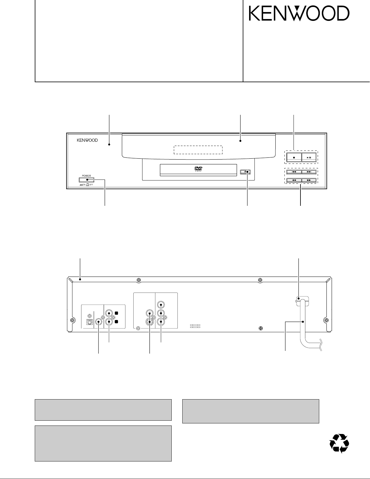
Front Panel *
(A60-)
Button(POWER) *
(K27-)
© 2001-5/B51-5731-00 (K/K) 3470
Window *
(B10)
Button *
(K27-)
Button(PLAY) *
(K27-)
Button(SKIP) *
(K27-)
Top cover *
(A01-)
RCA jack
(E63-1227-08)
RCA jack
(E63-1226-08)
In compliance with Federal Regulations, following are reproduction of labels on, or inside the porduct relating to laser
product safety.
KENWOOD-Crop. certifies this equipment conforms to DHHS
Regulations No.21 CFR 1040. 10, Chapter 1, subchapter J.
DANGER : Laser radiation when open and interlock
defeated.
AVOID DIRECT EXPOSURE TO BEAM.
RCA jack *
(E63-)
RCA jack
(E63-1191-08)
AC power cord bushing
(J42-0350-08)
AC power cord *
(E30-)
* Refer to parts list on page 18 .
Caution : No connection of ground line if disassemble
the unit. Please connect the ground line on
rear panel, PCBs, Chassis and some others.
DV-502/503/DVF-3050/3550
CONTENTS / ACCESSORIES / CAUTIONS
Contents
CONTENTS / ACCESSORIES / CAUTIONS............. 2
DISASSEMBLY FOR REPAIR....................................3
BLOCK DIAGRAM ......................................................4
CIRCUIT DESCRIPTION ............................................5
WIRING DIAGRAM ...................................................10
Attention
Please contact our KENWOOD Service Department in your side if you want the service information; Circuit Description. Full
Described Parts list and so. Information is available to you by internet from us.
Accessories
PC BOARD .............................................................. 11
SCHEMATIC DIAGRAM .......................................... 15
EXPLODED VIEW ....................................................21
PARTS LIST..............................................................22
SPECIFICATIONS ......................................Back cover
Cord RCA 1p
(E30-7235-08)
Batteries (R03/AAA) (2)
Cord RCA 3p
(E30-2990-08)
Remote control unit (1)
(A70-1532-08)
Cautions
Note related to transportation and movement
Before transporting or moving this unit, carry out the following operations.
1. Set the POWER key to ON without loading a disc.
2. Wait a few seconds and verify that the display shown
appears.
3. Set the POWER key to OFF.
*AC plug adaptor (1)
(E03-0115-05)
* Use to adapt the plug on the
power cord to the shape of the
wall outlet.
(Accessory only for regions
where use is necessary.)
Beware of condensation
When the difference between the internal temperature of the unit
and external atmosphere is large, dew (mist) may be produced on
the internal parts of the unit. In such a case, turn the unit ON and
leave it for a few hours until the condensation has dried up.
Be especially careful in the following conditions:
When the unit is brought into a place where there is a large difference in temperature between the previous location, when the
humidity of the listening room is high, etc.
Operation to reset
The microprocessor may fall into malfunction (impossibility to operate erroneous display, etc.) when the power cord is unplugged
while power is ON or due to an external factor. In this case, execute the following procedure to reset the microprocessor and
return it to normal condition.
2
1 In POWER ON condition, keep the 7 (STOP) key and the ¡
(Search) key pressed at the same time.
2 When both keys are pressed, the region code of the unit, the
software version, etc. will be displayed on the display. (When
nothing is done, the display of this information continues.)
Example: 71 . 101 . 06:14
3 Press the ON/OFF key to go to Power OFF.
4 When Power ON is performed with the ON/OFF key, the set-
tings become the default factory settings.
¶ Please note that resetting the microprocessor clears the con-
tents stored in, it returns the microprocessor to the condition
when it left the factory.
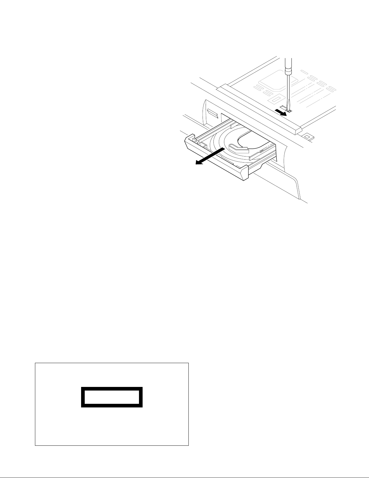
DISASSEMBLY FOR REPAIR
The marking is located on the rear panel and says that
the component uses laser beams that have been classified as Class 1. It means that the unit is utilizing laser
beams that are of a weaker class. There is no danger of
hazardous radiation outside the unit.
CLASS 1
LASER PRODUCT
The marking of products using lasers
(Except for some areas)
How to Remove Disc in unit
Slide the lever of the mechanism from bottom side as
figure if you can't get the disc on the tray.
DV-502/503/DVF-3050/3550
CAUTIONS
3
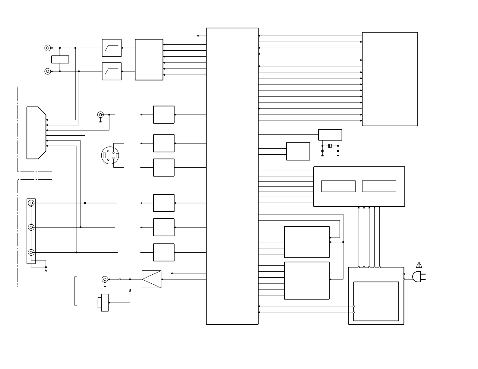
ADDR
F-WE
F-RESET
F-DE
D-RAS0-
ADDR
RDNOTWR
DATA
D-CAS0D-CAS1-
+3.3V DIGITAL VCC
F/E SDATA
EXIT-DATA
+3.3V-RESET
F/E SCL
EXIT-BCLK
EXIT-DATAVALID
EXT-PSTART/ERROR
+12V MOTOR VCC
+8V MOTOR VCC
+5V DIGITAL VCC
SLIDER-IN(DRAWER-CCW-CTRL)
SLIDER-OUT(DRAWER-CW-CTRL)
SLIDER-OPEN/CLOSE(POWER-POSITION-P1)
+12V ANALOG VCC
+8V ANALOG VCC
+5V DIGITAL VCC
-8V ANALOG VCC
+12V MOTOR VCC
5V FRONT
+8V MOTOR VCC
+3.3V DIGITAL VCC
: AC240V~ 50Hz
: AC230V~ 50Hz
(X)
(T,E)
: AC110-120V/220-240V~
: AC120V 60Hz
50/60Hz
(K,P)
(Y,M)
F-CE
F-OE(DRAM OE)
-27V
FL AC
FL AC
+5VS
STBY ON/OFF CNTL
IR REMOCON
+5.6VS
VFD DATA OUT
VFD STB
VFD DATA IN
PCM1748E-DATA
LRCLK
BCK
PCMCLK
PCM1748E-CS
PCM1748E-CLK
AUDIO-MUTE
CVBS-OUT
Y-OUT
R(Cr)-OUT
C-OUT
B(Cb)-OUT
G(Y)-OUT
9
10
8
6
7
SPDIF
PIXCLK-27MHz
SCL
SDA
VIDEO-MUTE
VFD CLK
DATA
IRQ2
POWER CTL
L AUDIO
R AUDIO
GND
BLUE-OUT
GREEN-OUT
RED-OUT
CVBS-OUT
L-CH OUT
R-CH OUT
IC201
STI5519
FLASH MEMORY
IC401
8MBIT
M29F400T-90N1
HY57V651610BLTC-8
SDRAM-64MBIT
IC301
F/E & MECHA
TVM MECHA
SMPS
IC901
UPD16311
DAC
PCM1748E
L.P.F
BA4560
IC802-A-A
MIXED
MUTE
VIDEO
JK803-A
S-VIDEO
JK701
Cr
Cb
Y
RCA 3V
COAXIAL
BUFFER
OPTICAL
IC501
74HCU04
M24CO2
EEPROM
IC202
SCART PART
RCA PART
HNV-06SS74
FL
125MHz
L.P.F
MIXED
R-CH
L-CH
TR
BUFFER
& B.N.F.
& B.N.F.
BUFFER
TR
& B.N.F.
BUFFER
TR
& B.N.F.
BUFFER
TR
& B.N.F.
BUFFER
TR
& B.N.F.
BUFFER
TR
CVBS-OUT
Y-OUT
C-OUT
R(Cr)-OUT
B(Cb)-OUT
G(Y)-OUT
CVBS-
TV SCART
JK804
ONLY
(E,T) TYPE
(E,T) TYPE
EXCEPT
DIGITAL OUT
MPEG
DV-502/503,DVF-3050
4
DV-502/503/DVF-3050/3550
BLOCK DIAGRAM
DV-502/503/DVF-3050/3550
CIRCUIT DESCRIPTION
1. MPEG: STI5519
Port No. Port Name I/O
Audio DAC
51 DAC SCLK O Over sampling clock EXT AUD CLOCK
52 DAC PCMOUT0 O PCM out 0 EXT AUD DATA
53 DAC PCMOUT1 - PCM out 1 (unused) EXT AUD REQ
54 DAC PCMOUT2 - PCM out 2 (unused)
55 DAC PCMCLK I/O PCM clock
56 DAC LRCLK O Left/Right clock EXT AUD WCLK
57 SPDIF OUT O SPDIF out
48 VDD PCM - VDD(+3V3)
49 VSS PCM - GND
Clock & Reset
124 RESET I Chip reset
122 VDD PLL - VDD PLL
123 VSS PLL - GND
120 PIX CLK I 27MHz main clock
PIOs and communication
186 PIO0(0) T STROBE I/O PIO0(0) UART0 data
187 PIO0(1) MOD SW I/O PIO0(1) ATAPI RD
188 PIO0(2) VFD STB I/O PIO0(2) ATAPI WR
189 PIO0(3) VFD CLK I/O PIO0(3)
190 PIO0(4) VFD DATA OUT I/O PIO0(4)
191 PIO0(5) VFD DATA IN I/O PIO0(5)
PIO0(6) SLIDER SENSOR
192 OPEN/CLOSE I/O PIO0(6)
(DRAWER POSITION)
193
194 PIO1(0) SDA I/O PIO1(0) SSC0 data (MTSR out/MRST in)
195 PIO1(1) SCL I/O PIO1(1) SSC0 clock
196
197 PIO1(3) TXD(JIG) I/O PIO1(3) UART2 TXD
200 PIO1(4) RXD(JIG) I/O PIO1(4) UART2 RXD
201 PIO1(5) FRONT TXDI I/O PIO1(5) PARA SYNC UART1 RXD
202 TRIGGER IN I/O Trigger in for DCU
203 TRIGGER OUT I/O Trigger out for DCU
204 PIO2(0) H/P IND I/O Unused
205 PIO2(1) FRONT RXD I/O Unused
206 PIO2(2) MIC IN - Unused
207 PIO3(8) MIC OUT - Unused
208 PIO2(4) AUDIO MUTE I/O Audio mute
10 PIO3(4) IR REMOCON I/O PIO3(4) PARA DATA(4)/CAPTURE IN1 UART1 RTS(RTS1)
11 PIO3(5) I/O Unused PARA DATA(5)/CAPTURE IN2 UART2 RTS(RTS2)
12 PIO3(6) I/O Unused
PIO0(7) SLIDER IN
(DRAWER CCW/CTRL)
PIO1(2) SLIDER OUT
(DRAWER CW CTRL)
1 PIO2(5) RGB SEL(BLANK) I/O RGB sel.(blank)
2 PIO2(6) VIDEO MUTE I/O Video mute
3 PIO2(7) 16: 9 INDICATOR I/O 16 : 9 indicator
6 PIO3(0) SCART H(TV/AUX) I/O PIO3(0) PARA DATA(0)
7 PIO3(1) POWER CTL I/O PIO3(1) PARA DATA(1)
8 PIO3(2) I/O Unused PARA DATA(2)
9 PIO3(3) I/O Unused PARA DATA(3)/CAPTURE IN0
I/O PIO0(7)
I/O PIO1(2) PARA DVALID
Main Alternate function
Function Input Output
PARA DATA(6)/UART1 CTS
(CTS1)
Note: Port list sorted by function for MPEG IC
COMP OUT1
5

DV-502/503/DVF-3050/3550
CIRCUIT DESCRIPTION
Port No. Port Name I/O
13 PIO3(7) DVD RESET I/O PIO3(7)
39~46 PIO4(0~7) I/O PIO4(0~7) YC(0~7)
Reserved
20 B WCLK I/O Unused
21 B V4 I/O Unused
22 NRSS OUT I/O Unused
103 ADC SCLK I/O Unused
104 ADC LRCK I/O Unused
105 ADC DATA I/O Unused
106 ADC PCMCLK O Unused
EMI Interface
161~170 CPU ADR(1~10) O ADR(1~10)
173~183 CPU ADR(11~21) O ADR(11~21)
141~148 CPU DATA(0~7) I/O DATA(0~7)
151~158 CPU DATA(8~15) I/O DATA(8~15)
138 CPU RAS1 I/O Unused
131 CPU WAIT I Connected to GND
130 CPU RW O READ NOT WRITE
128 CPU BE(0) O BYTE 0 ENABLE
129 CPU BE(1) O BYTE 1 ENABLE
139 CPU CAS0 O DRAM CAS0
140 CPU CAS1 O DRAM
135 CPU CE(0) O DRAM RAS0
134 CPU CE(1) O Chip Sel. BANK1
133 CPU CE(2) O Chip Sel. BANK2
132 CPU CE(3) O Chip Sel. BANK3
118 CPU PDR CLK O SDRAM clock
117 CPU OE I/O Output enable
Interrupt
127 IRQ(0) I Unused
126 IRQ(1) I Unused
125 IRQ(2) I IRQ(2) (MD IRQ)
Timers
116 PWM0 I/O Unused HSYNC
115 PWM1 I/O Pulse width modula o Boot from ROM3
114 PWM2 I/O Unused VSYNC
JTAG
113 TCK I Test clock
112 TDI I Test data in
111 TDO O Test data out
110 TMS I Test mode select
109 TRST4 I Test reset
Front-end
16 B DATA I 12S data SER Data
17 B BCLK I 12S bit clock SER BCLK
18 B FLAG I 12S error flag DVD SER VALID
19 B SYNC I 12S selector/ABS time SER SYNC
Video DAC
27,26,25 R/G/B (OUT) O R/G/B output
32~34 Y/C/CV (OUT) O Y/C/CV output
29 I REF RG I I REF DAC RGB
28 V REF RG I V REF DAC RGB
Main Alternate function
Function Input Output
PARA DATA(7)/UART2 CTS
(CTS2)
COPM OUT0
6
DV-502/503/DVF-3050/3550
CIRCUIT DESCRIPTION
Port No. Port Name I/O
36 I REF YCC I I REF DAC YCC
35 V REF YCC I Y REF DAC YCC
23 VDD RGB - YDDA RGB =2.5V
24 VSS RGB - GND
30 VDD YCC - YDDA YCC =2.5V
31 VSS YCC - GND
Shared memory interface
69~66 SMI ADR(0~3) O Address bus SDRAM
58~63 SMI ADR(4~9) O Address bus SDRAM
70~73 SMI ADR(10~13) O Address bus SDRAM
84~93 SMI DATA(0~15) I/O Data bus SDRAM
97~102
74,75 SMI CS(0,1) O Chip select bank 0,1
76 SMI RAS O RAS SDRAM
77 SMI CAS O CAS SDRAM
78 SMI WE O SDRAM write enable
79,80 SMI DQML, U O
82 SMI CLKIN I SDRAM clock in
95 SMI CLKOUT O SDRAM clock out
Power supply
4,47,81,107
136,159,184
14,37,64
94,119,149 VDD2 5 - 2.5V Power supply
171 198
5,15,38,50
65 83,96
108,121,137 VSS - GND
150,160,172
185,199
VDD3 3 - 3.3V Power supply
DQ MASK EN LOW,
UP
Main Alternate function
Function Input Output
2-1 VFO controller : uPD16311(IC901)
Pin No. Pin Name I/O Description
6 DIN I Inputs serial data at rising edge of shift clock,starting from lower bit.
5 DOUT O
9 STB - Strobe pin.
8 CLK I Reads serial data at rising edge, and output data at falling edge.
52 OSC - Connect resistor for determining oscillation frequency to this pin.
15~26 S1/KS1~S12/KS12 O Segment output pins (Dual function as key source).
44~39 G1~G6 O Grid output pins.
27~32 S13/G16~S18/G11
35,36 S19/G11,S20/G19
50~46 LED1~LED5 O Unused.
10~13 KEY1~KEY4 I Data input to these pins is latched at end of display cycle.
1~4 NC - Unused.
14,33,45 VDD - +5V power supply.
51 VSS - Connect this pin to GND of system.
34 VEE - -35V power supply.
7 NC - Unused.
Output serial data at falling edge of shift clock,starting from lower bit.
This is N-ch open-drain output pin.
O These pins are selectable for segment or grid output.
7
 Loading...