Kenwood DPSG-7 Service manual

COMPACT DISC PLAYER
70%
60
repeat 7
¢4
1
timespace
compact disc player
D.R.I.V.E.with 24bit D/A converter
on/standby
24bit Fine D.R.I.V.E.
'
603616617
651 606 604 650
OPTICAL
SYSTEM
CONTROL
DIGITAL OUT
PLAY OUT
R
L
DP-SG7/SG7G
SERVICE MANUAL
© 1999-7/B51-5542-00 (K/K) 2299
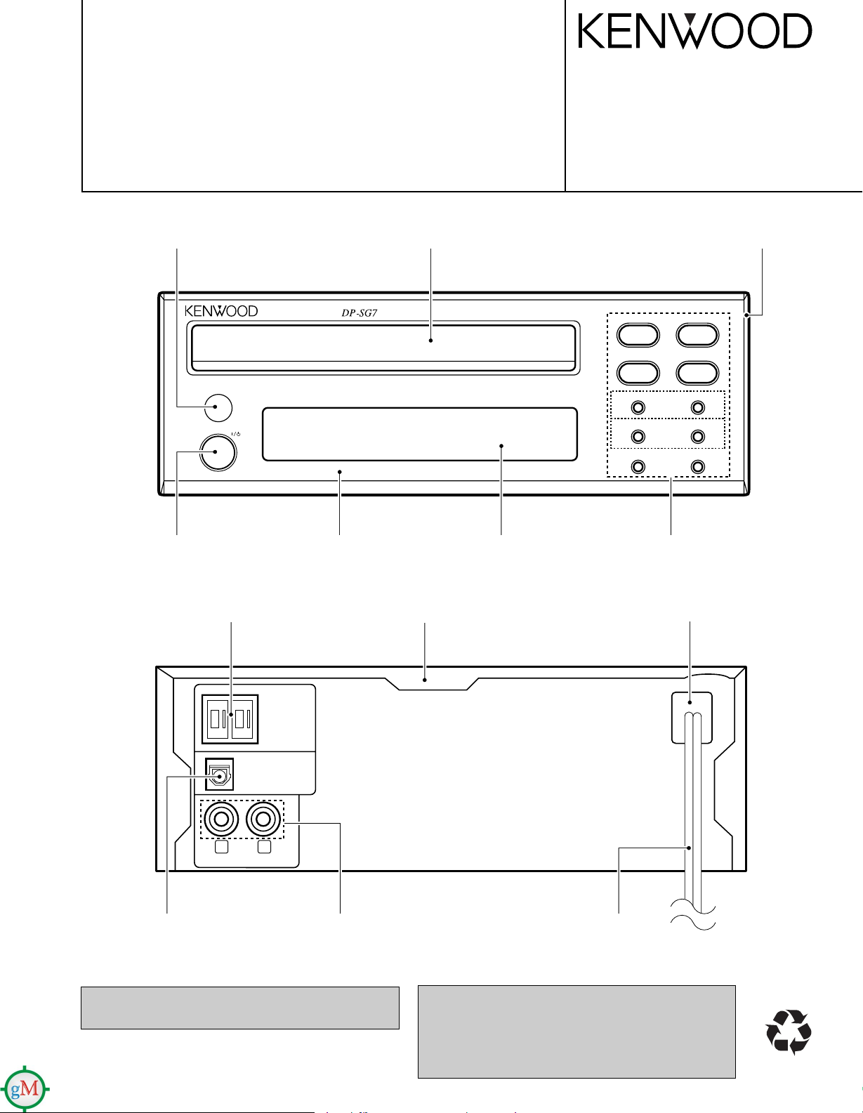
Indicator
(B12-0318-04)
Knob (POWER)
(K29-6741-04)
Rectangular receptacle
(E08-0312-05)
Panel
(A60-1671-03)
Panel
(A29-1058-03)
Metallic cabinet
(A01-3313-01)
Front glass
(B10-2372-03)
SUB panel
(A22-1778-31)
Knob
(K29-7571-03)
Power cord bushing
(J42-0083-05)
Oscillating module
(W02-1114-05)
In compliance with Federal Regulations, following are reproductions of labels on, or inside the product relating to laser
product safety.
Refer to DP-SE7 service manual (B51-5371-00),
if require the circuit description.
Phono jack
(E63-0122-05)
AC power cord *
(E30-)
* Refer to parts list on page 15.
KENWOOD-Crop. certifies this equipment conforms to
DHHS Regulations No. 21 DFR 1040. 10, Chapter 1, Subchapter J.
DANGER : Laser radiation when open and interlock
defeated.
AVOID DIRECT EXPOSURE TO BEAM
Illustration is DP-SG7.

DP-SG7/SG7G
Operation to reset
The microcomputer may fall into malfunction (impossibility to operate, erroneous display, etc.) when the
power cord is unplugged while power is ON or due
to an external factor . In this case, execute the following procedure to reset the microcomputer and return
it to normal condition.
DP-SG7
Pull the power plug from the receptacle, and then
plug it in again.
÷ Please note that resetting the microcomputer clears
the contents stored in it returns it to condition when it
left the factory.
CONTENTS / CAUTIONS
Contents
CONTENTS / CAUTIONS.......................................... 2
DISASSEMBLY FOR REPAIR....................................3
ADJUSTMENT............................................................4
PC BOARD ................................................................ 5
SCHEMATIC DIAGRAM............................................ 7
EXPLODED VIEW ....................................................13
PARTS LIST..............................................................15
SPECIFICATIONS ......................................Back cover
Cautions
2

DISASSEMBLY FOR REPAIR
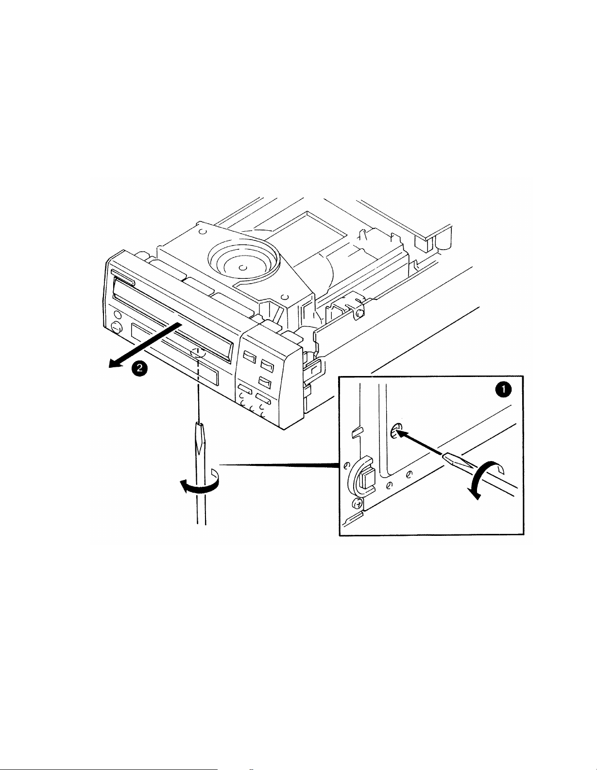
How to open tray if not comes out.
1. Insert screwdriver to hole on bottom plate and turn screw
clockwisely about 100° (1).
2. Pull tray out by hand if tray comes out (2).
DP-SG7/SG7G
3

DP-SG7/SG7G
VC
CN3
L.P.F.
+
+
L.P.F.
VTVM
VTVM
1
2
3
4
5
6
7
1.2 kHz
50 mVrms
RF
FE1
FE2
VC
TE2
TE1
S.S
+
_
T-GAIN
VR3 VR1 VR2
CN1
TE-B FE-B
ADJUSTMENT
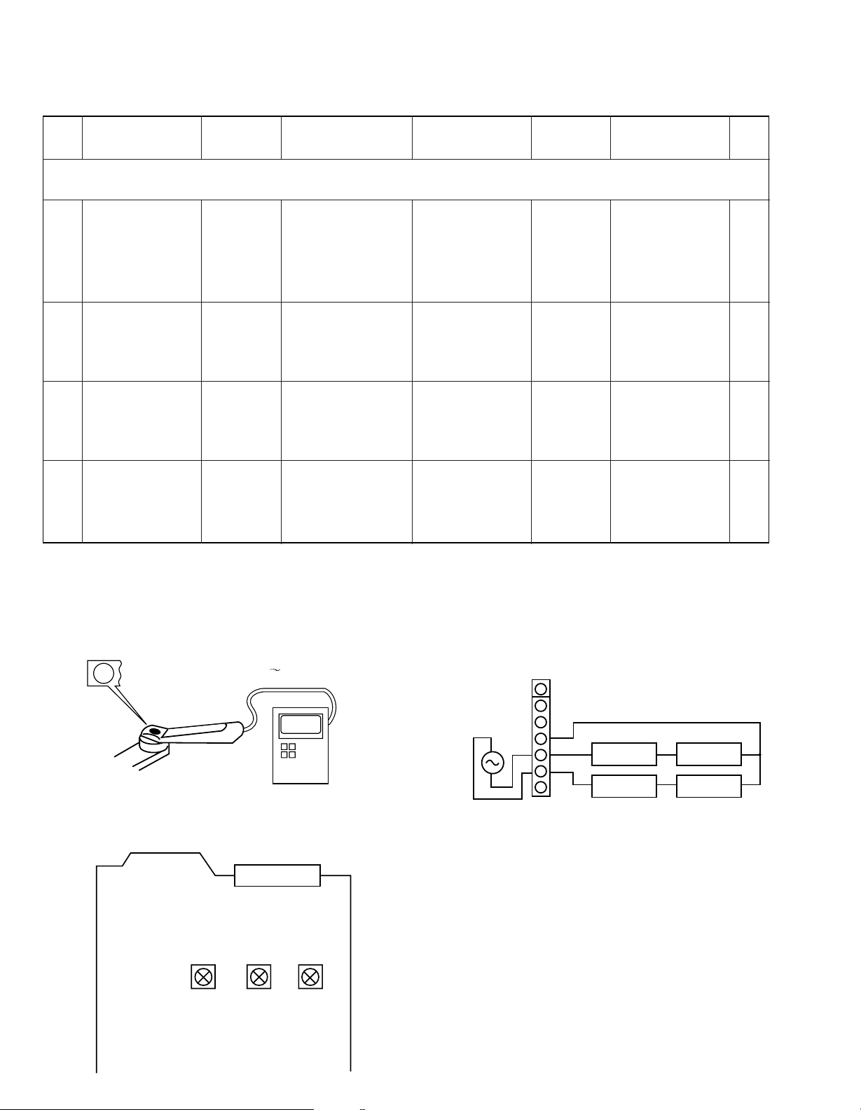
No. ITEM
While pressing the "REPEAT" key, turn the AC ON.
{ Refer to test mode (MODE 0 0) }
1 LASER POWER
FOCUS ERROR
2
3
Note:
Type 4 disc : SONY YEDS-18 Test Disc or equivalent.(KTD-0✽)
LPF: Around 47 kΩ+ 390 pF or so.
Step 1~4 are in Test Mode.
BIAS
TRACKING ERROR
BALANCE
INPUT
SETTINGS
−
Test disc
Type 4
Test disc
Type 4
Test disc
Type 4
Apply signal of
1.2 kHz,
50mVrms to
CN3 pin 5-6.
OUTPUT
SETTINGS
Apply the sensor section
of optical power meter
on the pickup lens.
Connect an oscilloscope
as follows.
CH1 : RF (CN3 pin 1)
CH2 : TE (CN3 pin 6)
Connect an oscilloscope
as follows.
CH1 : RF (CN3 pin 1)
CH2 : TE (CN3 pin 6)
Connect a LPF to CN3
pin 5-6 to which you
connect an oscilloscope
or AC voltmeters.
PLAYER
SETTINGS
Press the
PLAY/PAUSE key,
then confirm that the
LED is "03".
Press the
PLAY
/PAUSE
then confirm that the
LED is "05".
Press the
PLAY/PAUSE key,
then confirm that the
LED
Press the
PLAY/PAUSE key,
then confirm that the
LED
key,
is "03".
is "05".
ALIGNMENT
POINTS
−
FE BIAS
VR2
TE BALANCE
VR1
TRACKING
GAIN
VR3
ALIGN
FOR
On the power from
0.08 to 0.15 mW,
when the diffraction
grating is correctly
aligned with the RF
level of 0.6 Vp-p or
more.
Optimum eye pattern
Symmetry between
upper and lower pat-
terns
Two VTVMs should
read the same value.
FIG.
(a)
(e)4 TRACKING GAIN
(e) Tracking gain(a) Laser power
0.08 0.15 mW
Pickup
Optical power meter
ALIGNMENT POINTS
4

ACEGIBDFHJ
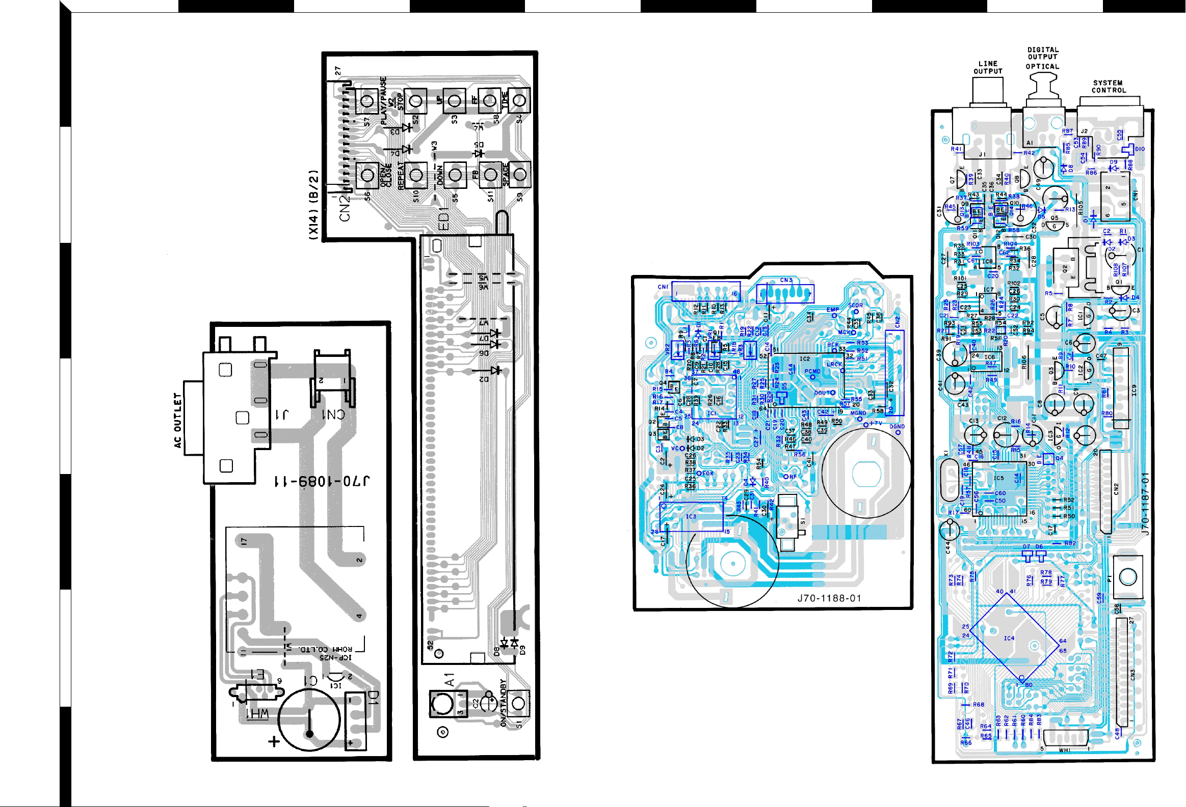
PC BOARD(Component side view
1
2
3
)
ELECTRIC UNIT
(X25-6100-01)
CD PLAYER UNIT
(X32-3600-00)
4
5
6
DISPLAY UNIT
7
Refer to the schematic diagram for the value of resistors and capacitors.
(X14-4760-21)
5 6
 Loading...