Kenwood DPFJ-9030, CD-4900-M Service manual
70%
MULTIPLE COMPACT DISC PLAYER
DISC SKIP
$ ›
&
^
o PUSH OPEN
)
REPEAT
CONFIRM
DISPLAY
CONTINUROUS PLAY
RANDOM
OPERATION
TIMER PLAY
DISPLAY|B
OFF ON
STANDBY
POWER
ON/STANDBY
DISPLAY|A
B A
R
L
OUTPUT SYSTEM
CONTROL
SL16
TEXT
TEXT
DIGITAL
OUT
OPTICAL
A
B
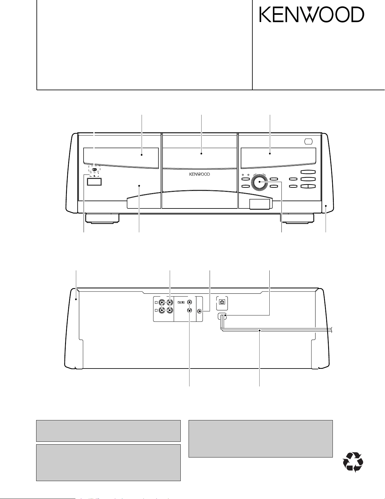
CD-4900M/DPF-J9030
SERVICE MANUAL
© 2000-1/B51-5594-00 (K/K) 2738
Knob(TIMER)
(K29-7717-08)
Indicator
(B12-0326-04)
Metallic cabinet
(A01-3738-08)
Front glass
(B10-3557-08)
Dressing panel *
(A21-)
Phono jack
(E63-0120-05)
Front glass
(B10-3558-08)
Miniature phone jack
(E11-0360-05)
Front glass
(B10-3559-08)
knob
(K29-7716-08)
Power cord bushing
(J42-0083-05)
Panel
(A60-1752-18)
Miniature phone jack
(E11-0293-05)
In compliance with Federal Regulations, following are reproductions of labels on, or inside the product relating to laser
product safety.
KENWOOD-Crop. certifies this equipment conforms to DHHS
Regulations No. 21 DFR 1040. 10, Chapter 1, Subchapter J.
DANGER : Laser radiation when open and interlock
defeated.
AVOID DIRECT EXPOSURE TO BEAM
AC power cord *
(E30-)
* Refer to parts list on page 26.
• Please refer to the service manual CD-223M/DPFJ3010/CD-224M/DPF-J5010 (B51-5409-00) if need more
information.
• Refer to CD-2260M/2280M/DPF-J7010/J9010 service manual (B51-5416-00), if you require sub microprocessor (IC3:
X25) in detail.
Audio
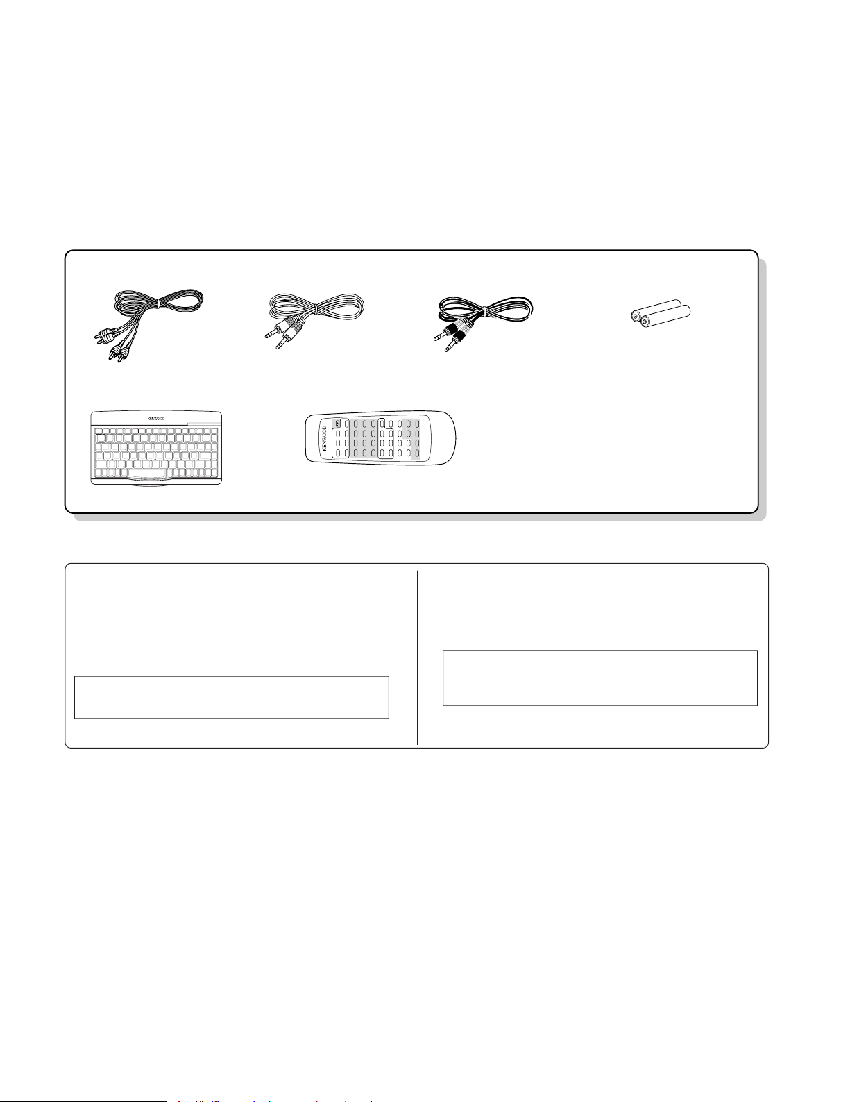
(E30-0505-05) (E30-2816-05) (E30-2861-05)
cord ....................... (2)
System control cord ........ (1)
Batteries (R6/AA) ............ (2)
Communication cord ....... (1)
REMOTE CONTROL UNIT RC-KB2
REMOTE CONTROL UNIT
RC-P0714
T
U
V
X
Y
Z
W
/
.
–
(
'
)
MODE
SET
SELECTOR
DISC
DELETE
/CLEAR
SPACE CHARAC.
/CHECK /P.MODE
RANDOM
SELECTON
DISPLAY
CONFIRM
A
B
C
D
E
F
G
REPEAT
BEST
POWER
32
4
H
J
K
L
M
N
O
P
Q
R
S
1
76
8
5
+100 +100
9
7
ENTER
6
4¢
1¡
DISC SKIP
DOWN UP
CURSOR
CHARACTER
DOWN
UP
LEFT RIGHT
I
Remote control units
...... (2)
(A70-1326-05): RC-KB2
Battery cover (A09-1176-08)
(A70-1335-18): RC-P0713
Battery cover (A09-0374-08)
To reset the registered contents
The registered contents for title, music type, user file and best
selection can be reset by the following procedure.
Operation to reset
The microcomputer may malfunction (impossibility to operate,
erroneous display, etc.) when the connection cords are unplugged while power is ON or due to an external factor. In this
case, execute the following method to reset the microcomputer
and return it to normal condition.
Unplug the power cord from the power socket and plug the
power cord into the socket again.
Unplug the power cord from the power socket, and while
holding the 7 key depressed, plug the power cord into the
socket again.
CD-4900M/DPF-J9030
CONTENTS / ACCESSORIES / CAUTIONS
Contents
CONTENTS / ACCESSORIES / CAUTIONS............. 2
CIRCUIT DESCRIPTION............................................3
ADJUSTMENT............................................................8
PC BOARD ................................................................ 9
Accessories
SCHEMATIC DIAGRAM.......................................... 13
EXPLODED VIEW ....................................................24
PARTS LIST..............................................................26
SPECIFICATIONS ......................................Back cover
Cautions
2
CD-4900M/DPF-J9030
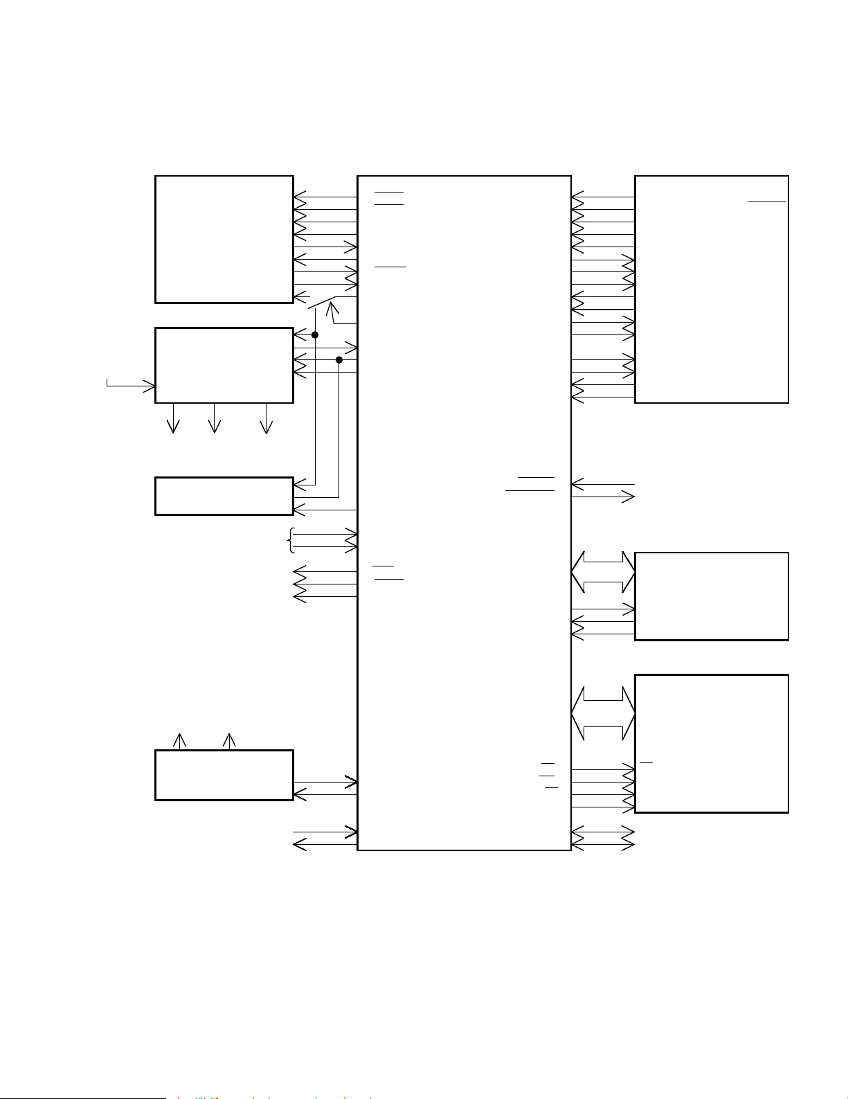
X32,IC2 X32,IC8 CD MECHA
CXD2587Q CLOCK 35 CLOK S1 SW 7 S1 SW
CDM-31
(DSP) XLAT 36 XLAT S2 SW 4 S2 SW
DATA 44 DATA S3 SW 3 S3 SW
SCLK 33 SCLK D SENS1 23 DISC SW1
SENS 34 SENS D SENS2 60 DISC SW2
SYSM 45 MUTG +5V PUL 10 D PWM
SCOR 46 SCOR R CW 24 ROTARY+
SQCO 73 SQSI R CCW 25 ROTARY-
SQCK 75 SCK/SQCK LOAD SW 28 LOAD SW1
UNLOAD SW 29 UNLOAD SW1
X32,IC14 67 SCK SW LOAD M+26 LOADM+1
uPD780204
CLK
LOAD M-27 LOADM-1
(DOT DRIVER)
SO 72 SI
TIMER PLAY SI 74 SO LOADM+2 63 LOADM+2
ON/OFF STB 71 STB1 LOADM-2 62 LOADM-2
7P LOAD SW2 58 UNLOAD SW2
4P 5P 6P UNLOAD SW2 59 DLE SW2
uPD784217GF502
ON/ LED A LED B
STANDBY
X32,IC15
uPD780204 CLK
RESET 43 RESET INPUT
(DOT DRIVER)
SI
IC RESET 47 PERIPHERY IC RESET
STB 46 STB2
JOG
55 JOG 2
X32,IC10
56 JOG 1
14~21 D0~D7
LASER ON/OFF 70 LDC (D7~D0) uPD17215GT-737
ANALOG MUTE 48 SYSM
SPINDLE MOTOR ON/OFF 31 MON
RWRREQ 13 RWRREQ
RTREN 11 RTREN
8.16BIT 54 8,16 RWR 12 RWR
MODEL DISCRIMINATION 53 A/D0
X32,IC9
84~91
(D0~D7)
A1 SW A2 SW
1,76~83,92~99
(A0~A16) (SRAM)
P1 P2
RD 5 OE
uPD780024
RXD0 69 TXD1 WR 6 WE
(SUB uCOM)
TXD0 68 RXD1 CS 7 CS
ASTB 8 LE
TX OUT 65 TXD2 SDATA 49 SERIAL COMMUNICATION
RECEIVER
66 RXD2 SBUSY 50
CIRCUIT DESCRIPTION
1. Main microprocessor : uPD784217GF502 (X32, IC8)
1-1 Microprocessor periphery block diagram
3

CD-4900M/DPF-J9030
CIRCUIT DESCRIPTION
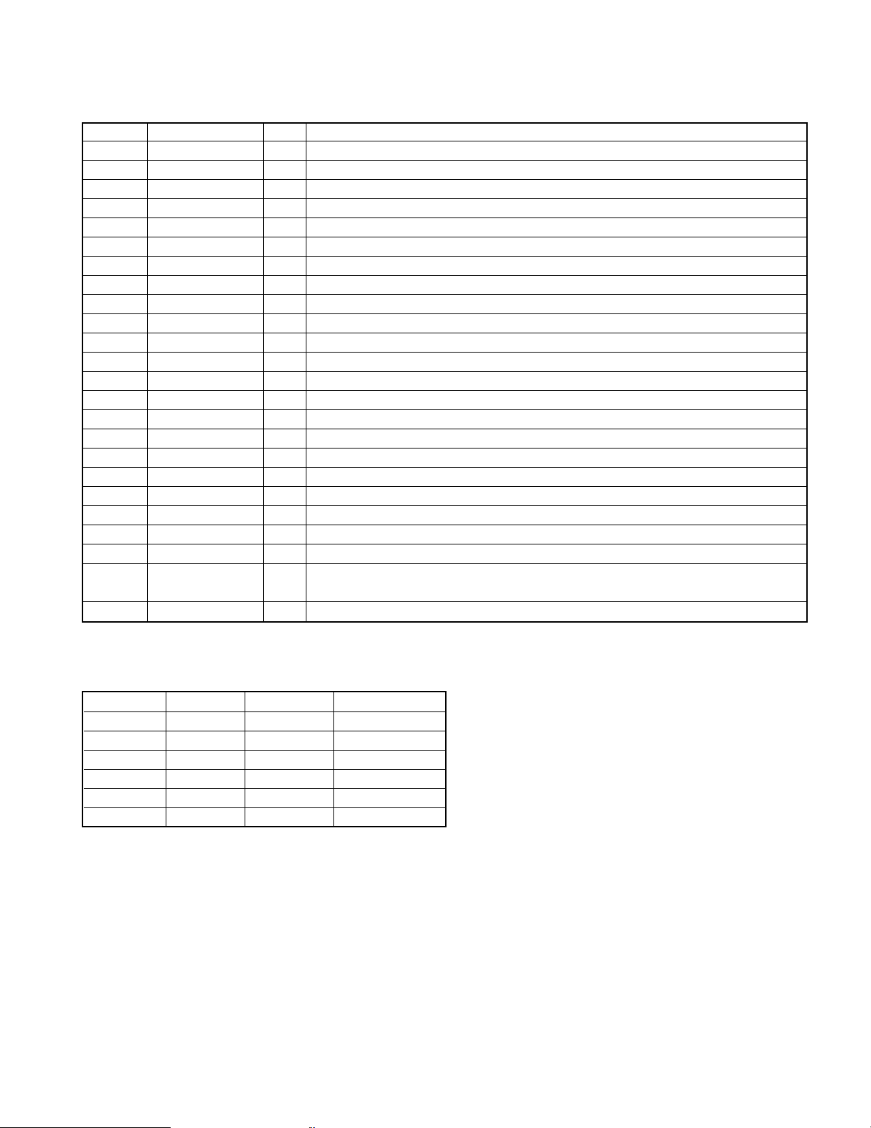
1-2 Microprocessor pin description (X32, IC8): UPD784217GF502
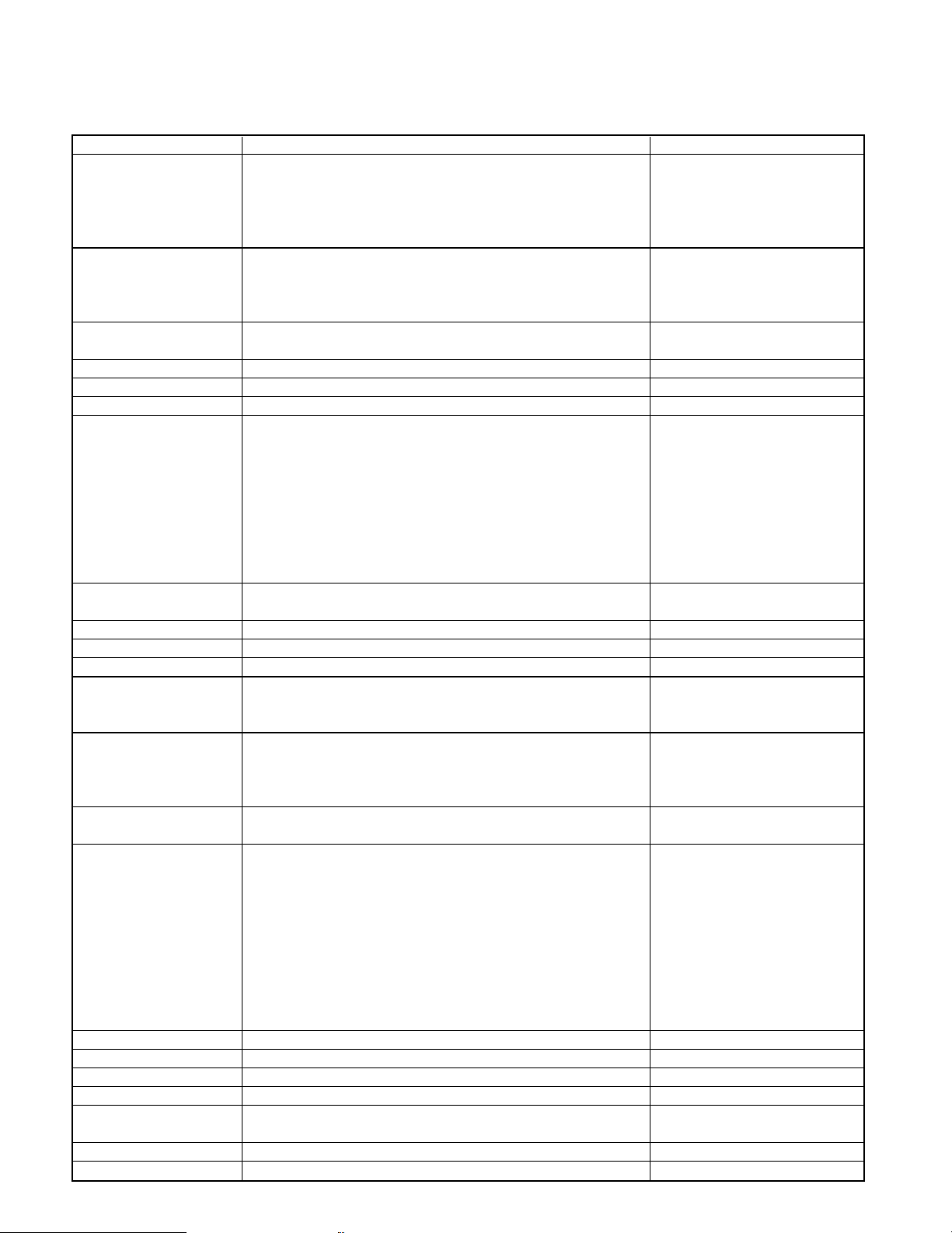
Pin No. Pin Name I/O Description
1 A2 O Address bus of SRAM.
2 NC - No connection.
3 S3-SW I Mechanism address detector switch.
4 S2-SW I Mechanism address detector switch.
5 RD O SRAM read strobe.
6 WR O SRAM write strobe
7 S1-SW I Mechanism address detector switch.
8 ASTB O No connection.
9 VDD - Power supply(+5V).
10 +5VPUL O Disc sensor ON/OFF. L:on
11 RTRN I TX permission data to remote control microprocessor.
12 RWR I Reading data of remote control microprocessor.
13 RWRR O TX request data to remote control microprocessor.
14~21 L-D7-D0 O Data output to remote control microprocessor.
22 TEST - GND.
23 DISC-SW I Disc sensor.
24 ROTARY-CW O Mechanism rotary motor(+). H:CCW
25 ROTRAY-CCW O Mechanism rotary motor(-). H:CW
26 LOADM+1 O Loading motor(+) for main pickup.
27 LOADM-1 O Loading motor(-) for main pickup.
28 LOAD-SW1 I Loading switch for main pickup.
29 UNLOAD-SW1 I Unloading switch for main pickup.
30 CS O Chip selector
31 MON O Control port of poor focus works.
32 SCLK O Sens serial data read clock.
33 SENS I SENS signal input.
34 CLOCK O Serial data clock.
35 XLAT O CXD2587Q latch. H î L:latch
36 DATA O Serial data output.
37 VDD - Power supply(+5V).
38,39 X1,2 - Main system clock(12.5MHz).
40 VSS - GND.
41 XT2 - No connection.
42 XT1 I GND.
43 RESET I System reset signal input.
44 SCOR I Sub code synchro detection.
45 MUTEG O Muting control output. H:muting on.
46 STB2 O Strobe signal output to dot driver.
47 ICRESET O IC reset.
48 SYSM O Analog muting. L: Muting on.
49 SDATA I/O Serial data signal I/O.
50 SBUSY I/O Serial busy signal I/O.
51 AVDD - Power supply(+5V).
52 AVREF - A/D reference power supply.
53 A/D0 I Model discrimination.
54 8/16 I 8/16 bit selector. H:16bit.
55 JOG2 I Encoder signal A input.
4
CD-4900M/DPF-J9030
CIRCUIT DESCRIPTION
Pin No. Pin Name I/O Description
56 JOG1 I Encoder signal B input.
57 DOOR-SW I Door open/close detector switch.
58 LOAD-SW2 I Load switch2 for sub pickup.
59 UNLOAD-SW2 I Unload switch2 for sub pickup.
60 DISC-SW2 I Disc2 sensor.
61 VSS - GND.
62 LOADM-2 O Load motor(-) for sub pickup.
63 LOADM+2 O Load motor(+) for sub pickup.
64 AVREF1 - D/A reference power supply.
65 RXD2 I UART communication input.
66 TXD2 O UART communication output.
67 SQCK/SCK-SW O SQCK,SCK(DOT/DSP clock) selector. L:DSP.
68 RXD1 I UART communication input from sub u-com.
69 TXD1 O UART communication output to sub u-com.
70 LDC O Laser on/off. L: Laser diode on.
71 STB1 O Strobe signal output to dot driver.
72 SI I Data input from dot driver.
73 SQS1 I Sub code read data input.
74 SO O Data output to dot driver.
75 SCK/SQCK O Dot driver/sub code read clock.
76-83 A16,14,12,7-3 O Address output to SRAM.
84~91 D0-7 I/O SRAM data bus.
92~99
100 VSS - GND.
A10,A15,A13,A8,
A9,A11,A0,A1
O Address output to SRAM.
1-3 Key matrix ( ) : IC14 Pin No.
VOLTAGE A/D0(33) A/D1(32) A/D2(31)
4.1V - - OPERATION
3.3V - - RANDOM
2.5V - - CONFIRM
1.6V - REPEAT CONT.P
0.8V DOWN DISP. PLAY/PAUSE
0V UP POWER STOP
5
CD-4900M/DPF-J9030
CIRCUIT DESCRIPTION
2. Test mode
INPUT KEY PROCEDURE DISPLAY
Insert the AC plug to INITIAL CONDITION MECHA. INITIAL
the wall outlet with • Disc No.1 moves to the center. INITIAL OK!!
pressing the SKIP- • Clear the memory of the SRAM.
DOWN key. • Door opens. INITIAL NG
• Set the switch of TIMER ON PLAY to ON. TIMER NG
Insert the AC plug to CIRCUIT ADJUSTMENT TEST ON
the wall outlet with • Open the door and load the disc to the Disc No.1.
pressing the REPEAT • Close the door. The unit changes to test
key mode05 after clamping the disc.
PLAY/PAUSE Change the mode 05(tracking-on) and 05 XX:XX 03 XX:XX
03(tracking-off) alternately by the PLAY key.
STOP Stop the function. 00
UP The pickup travels outwards. MOTOR FORWARD
DOWN The pickup travels inwards. MOTOR REVERSE
RANDOM Shows the result of self-adjustment.
07 EF/FB 07 XXX:XXX
08 TG/FG 08 XXX:XXX
09 FE/RF 09 XXX:XXX
10 TE/VC 10 XXX:XXX
Mode changes alternately by the RANDOM key. NG: blinking
REPEAT Playback PGM signal of the Track No.7,13,23,30,34 and 41
in the order. And release the test mode.
CONFIRM Release the test mode.
(TIMER PLAY SW) Check the switch position. TIMER ON , TIMER OFF
OPERATION A/B Change the mechanism A and B.
Insert the AC plug to CHECK THE MECHANISM JAMMING.
the wall outlet with Clamp the Disc No1,2,100,50,200 and 199 in the order.
pressing the UP key.
Insert the AC plug to THE MECHANISM TEST MODE.
the wall outlet with Display shows Niagara until pressing any keys.
pressing the
RANDOM key.
PLAY/PAUSE Change the mode 05(tracking-on) and 05 XX:XX 03X:XX
03(tracking-off) alternately by the PLAY key.
STOP Stop the function.
Shows the result of self-adjustment.
07 EF/FB 07 XXX:XXX
08 TG/FG 08 XXX:XXX
09 FE/RF 09 XXX:XXX
10 TE/VC 10 XXX:XXX
Mode changes alternately by the STOP key. NG: blinking
UP Arm Motor Load operation. MOTOR LOAD
DOWN Arm Motor Unload operation. MOTOR UNLOAD
RANDOM Rotary Motor Clockwise turning. MOTOR CW
DISPLAY Rotary Motor Counterclockwise turning. MOTOR CCW
REPEAT Playback PGM signal of the Track No.7,13,23,30,34
and 41 in the order.And release the test mode.
CONFIRM Release the test mode.
OPERATION A/B Change the mechanism A and B.
6
ó
ó
ó
ó
ó
ó
í
ì
í
ì
ñ
ñ
ñ
ñ
ñ
ñ
ñ
ñ
ñ
ñ
ñ
ñ
ñ
ñ
ñ
ñ
ñ
ñ
CD-4900M/DPF-J9030
CIRCUIT DESCRIPTION
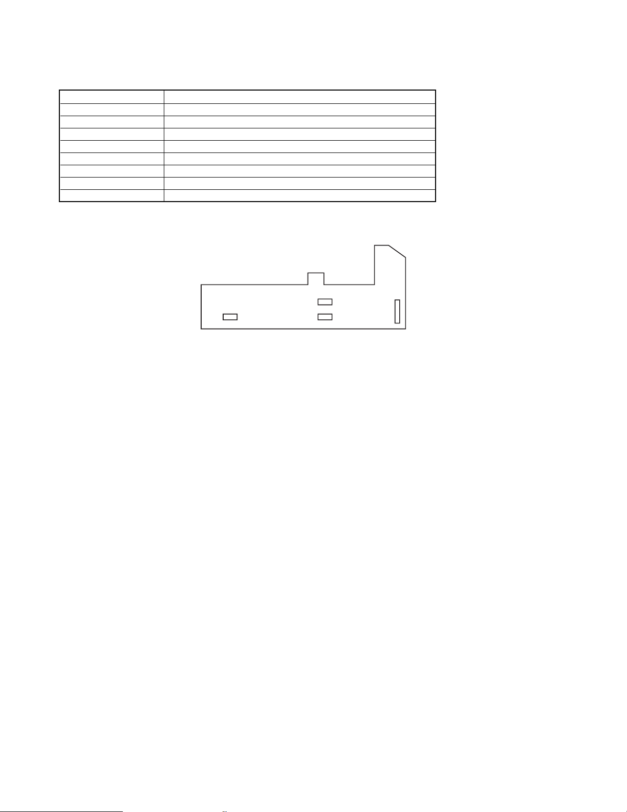
3. Error code
DISPLAY ERROR CONTENTS
MECHA ERROR 01 No input of S3. The original position error of Disc Number.
MECHA ERROR 02 No input of S2. The turning direction error to counterclockwise.
MECHA ERROR 03 No input of S1. The turning direction error to clockwise.
MECHA ERROR 04 No input of main load sw.
MECHA ERROR 05 No input of main unload sw.
MECHA ERROR 06 No input of sub load sw.
MECHA ERROR 07 No input of sub unload sw.
MECHA ERROR 08 No backed up(AC power cord has disconnected).
S1-3: Mechanism address detector switch.
There are load and unload switches in the main pickup.
SENSOR PCB
S2
S3
S1
S1 DISC 1~9
S2 DISC 10~99
S3 DISC 100~200
7
CD-4900M/DPF-J9030
ADJUSTMENT
No.
1. With pressing the REPEAT KEY, turn the power on to enter the test mode.
2. Set the Test disc to Disc NO. 1.
3. Close the door.
1
2
Note:
Type 4 disc :SONY YEDS-18 Test Disc or equivalent.
LPF : Around 47kΩ + 390 pF or so.
FIG. (d)
ITEM
FOCUS ERROR
BIAS
LASER CURRENT
CHECK
INPUT
SETTING
Test disc
Type4
/KTD-02
Test disc
Type4
OUTPUT
SETTING
Connect an oscillo-
scope as follows.
CH1:RF(X25, CN2-1
X32, CN2-1)
Connect the DC volt-
meter between Q1(E)
and VCC(CN1, 15pin)
on X25 and X32.
RF signal
PLAYER
SETTING
Press the PLAY
/PAUSE key .
Confirm that the
display is "05".
Press the PLAY
/PAUSE key .
Confirm that the
display is 03 or 05.
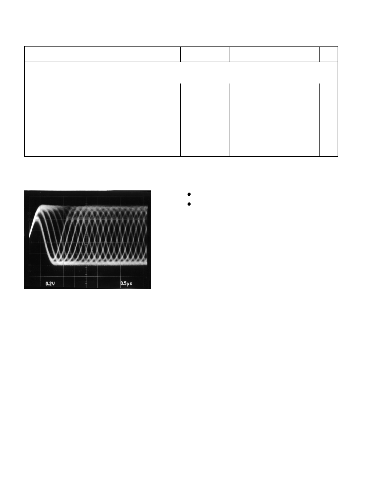
RF signal in test mode (PLAY).
Perform the tangential and focusing offset are focused into
one point on the display. The crossing points above and
below the center shall also be looked clearly. (FE BIAS)
ALIGNMENT
POINT
FE BIAS
VR1
(X25, X32)
–
ALIGN FOR
Optimum eye
pattern
0.5±0.2V
FIG.
(d)
8
 Loading...