Kenwood DPFJ-6030, CD-4700-M, CD-425-M, CD-4260-M Service manual
70%
MULTIPLE COMPACT DISC PLAYER
CD-425M/4260M/4700M
DPF-J6030
SERVICE MANUAL
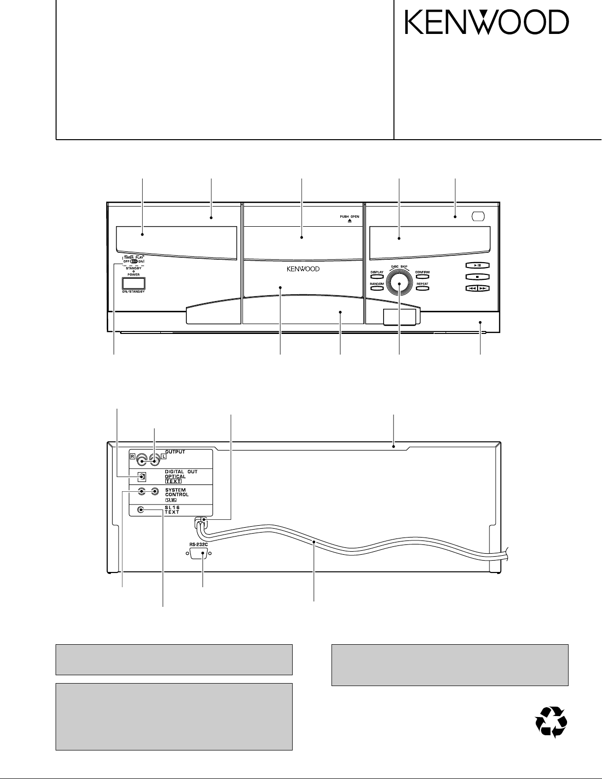
Front glass
(B10-3557-08)
Knob
(K29-7717-18)
Oscillating module
(W02-1114-15)
Pin jack
(E63-1078-05)
Dressing panel
(A21-3813-08)
Power cord bushing
(J42-0083-05)
Front glass
(B10-3558-18)
Dressing panel
(A21-3815-08)
Panel
(A29-1081-18)
© 2000-3/B51-5610-00 (K/K) 3037
Front glass
(B10-3559-08)
Knob
(K29-7716-18)
Metallic cabinet *
(A01-)
Dressing panel *
(A21-)
Panel
(A60-1753-38)
Miniature phone jack
(E11-0293-05)
Miniature phone jack
(E11-0360-05)
In compliance with Federal Regulations, following are
reproduction of labels on, or inside the porduct relating to
laser product safety.
KENWOOD-Crop. certifies this equipment conforms to
DHHS Regulations No.21 CFR 1040. 10, Chapter 1, Subchapter J.
DANGER : Laser radiation when open and interlock
defeated.
AVOID DIRECT EXPOSURE TO BEAM.
Rectangular receptacle
(E58-0024-05)
AC power cord
(E30-2883-05)
* Illustration is CD-4260M/4700M.
* Refer to parts list on page 18.
Refer to CD-223M/DPF-J3010 service manual (B51-5409-
00) if require the following items in detail.
1) Mechanism operation description.
2) Disassembly for repair.
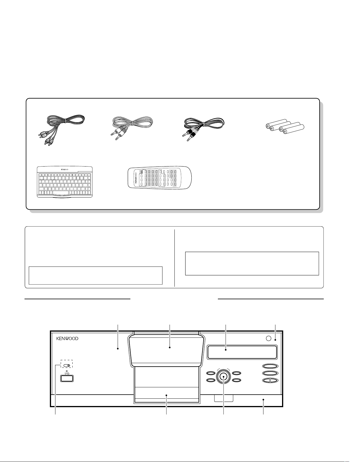
Audio
(E30-0505-05) (E30-2816-05) (E30-2861-05)
cord ....................... (2)
System control cord ........ (1)
Batteries (R6/AA) ............ (4)
Communication cord ....... (1)
REMOTE CONTROL UNIT RC-KB2
REMOTE CONTROL UNIT
RC-P0714
T
U
V
X
Y
Z
W
/
.
–
(
'
)
MODE
SET
SELECTOR
DISC
DELETE
/CLEAR
SPACE CHARAC.
/CHECK /P.MODE
RANDOM
SELECTON
DISPLAY
CONFIRM
A
B
C
D
E
F
G
REPEAT
BEST
POWER
32
4
H
J
K
L
M
N
O
P
Q
R
S
1
76
8
5
+100 +100
9
7
ENTER
6
4¢
1¡
DISC SKIP
DOWN UP
CURSOR
CHARACTER
DOWN
UP
LEFT RIGHT
I
Remote control units
...... (2)
(A70-1326-05): RC-KB2
Battery cover (A09-1176-08)
(A70-1336-18): RC-P0714
Battery cover (A09-0374-08)
To reset the registered contents
The registered contents for title, music type, user file, best selection and DTS disc can be reset by the following procedure.
Operation to reset
The microcomputer may malfunction (impossibility to operate,
erroneous display, etc.) when the connection cords are unplugged while power is ON or due to an external factor. In this
case, execute the following method to reset the microcomputer
and return it to normal condition.
Unplug the power cord from the power socket and plug the
power cord into the socket again.
Unplug the power cord from the power socket, and while
holding the 7 key depressed, plug the power cord into the
socket again.
CD-425M/4260M/4700M/DPF-J6030
TIMER PLAY
OFF ON
MULTIPLE COMPACT DISC PLAYER
ON/STANDBY
DISPLAY
DISC SKIP
0
PUSH OPEN
RANDOM
CONFIRM
REPEAT
6
7
4 ¢
200 DISC LOADING WITH TWIN PICK UP MECHANISM
STANDBY
CONTENTS / ACCESSORIES / CAUTIONS
Contents
CONTENTS / ACCESSORIES / CAUTIONS............. 2
EXTERNAL VIEW.......................................................2
CIRCUIT DESCRIPTION............................................3
ADJUSTMENT............................................................8
PC BOARD ................................................................ 9
Accessories
SCHEMATIC DIAGRAM.......................................... 11
EXPLODED VIEW ....................................................15
PARTS LIST..............................................................17
SPECIFICATIONS ......................................Back cover
Cautions
EXTERNAL VIEW
Dressing panel *
(A21-)
Front glass
(B10-2395-08)
Front glass
(B10-2396-18)
Dressing panel
(A21-3786-08)
2
Knob
(K29-6885-38)
Panel
(A29-1087-08)
Knob
(K29-6824-18)
* Illustration is CD-425M/DPF-J6030.
Panel
(A60-1755-18)
* Refer to parts list on page 17.
CD-425M/4260M/4700M/DPF-J6030
IC2 IC6 CD MECHA
CXD2587Q
CLOCK 35 CLOK S1_SW 56 S1_SW
(DSP) XLAT 36 XLAT S2_SW 28 S2_SW
DATA 44 DATA S3_SW 27 S3_SW
SCLK 33 SCLK D1_SW 58 DISC_SW1
SENS 34 SENS D2_SW 57 DISC_SW2
SYSM 45 MUTG
SCOR 46 SCOR R_CW 24 ROTARY+
SQCO 73 SQSI R_CCW 25 ROTARYSQCK 75 SCK/SQCK LOAD_SW 55 LOAD_SW
UNLOAD_SW 54 UNLOAD_SW
IC13 67 SCK_SW LOAD_P 31 LOADM+
uPD780232GC
CLK LOAD_M 30 LOADM-
(DOT DRIVER)
SO 72 SI
SI 74 SO
STB 71 STB RESET 43 RESET INPUT
REG_ON 29 PERIPHERY IC ON
T
IC RESET 63 PERIPHERY IC RESET
uPD784217GF501
TIMER PLAY
ON/OFF
SERIAL COMMUNICATION
49 SBUSY
50 SDATA
REMOCOM INPUT 48 REM
POWER KEY 47 POWER
JOG
60 JOG_2
59 JOG_1
DISC SENSOR ON/OFF 23 PWM
LASER ON/OFF 32 LDC
SPINDLE MOTOR ON/OFF 26 MON
DOOR OPEN/CLOSE 70 DOOR_SW
PROTECTION 53 PROTECT
IC10
ANALOG MUTE 10 RMUTE
84~91
(AD0~AD7)
CY62128L-70SC
(SRAM)
76~83,92~98
(A0~A14)
RD 5 OE
WR 6 WE
CS 7 CS
CIRCUIT DESCRIPTION
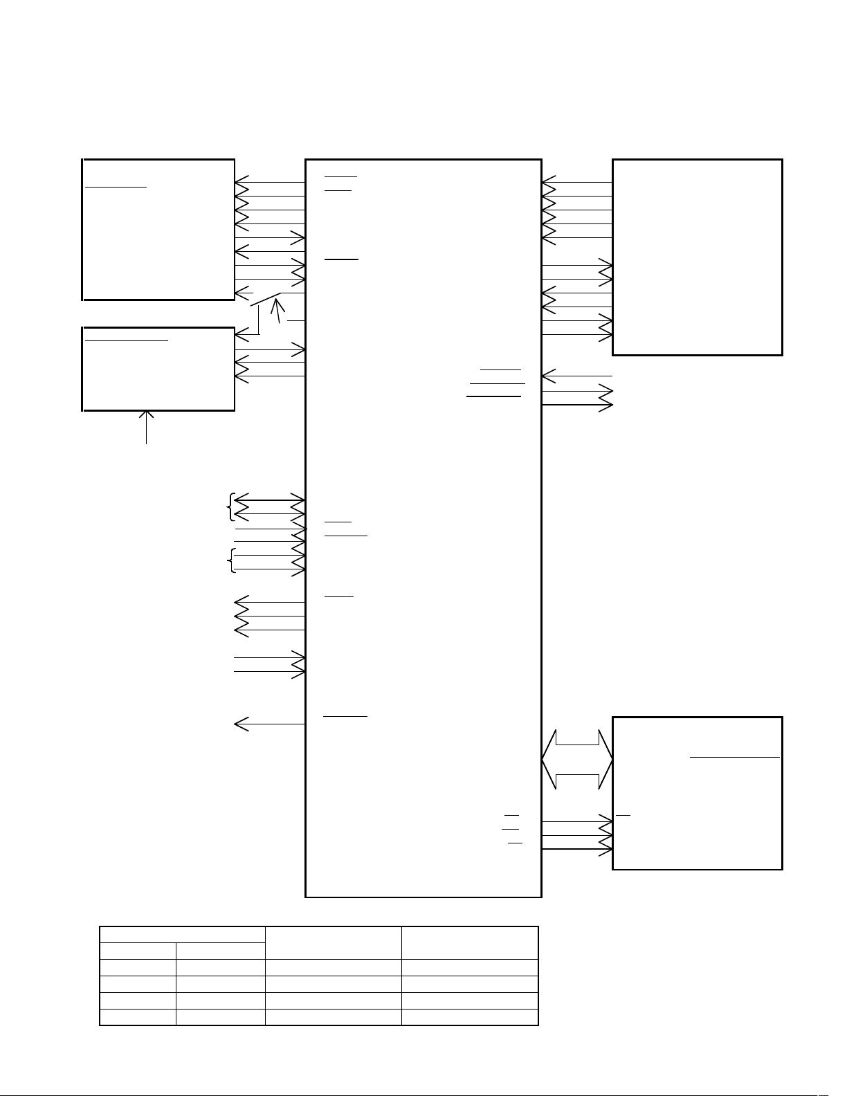
1. Main Microprocessor : uPD784217GF501
Microprocessor periphery block diagram
IMER_SW
2. Key matrix
PORT
VOLTAGE RESISTER
2.9V 5.1K RANDOM REPEAT
2.0V 3K DISPLAY CONFIRM
1.2V 2K STOP DOWN
0.4V SHORT PLAY UP
A/D 0(IC13,22pin) A/D 1(IC13,21pin)
3
CD-425M/4260M/4700M/DPF-J6030
CIRCUIT DESCRIPTION
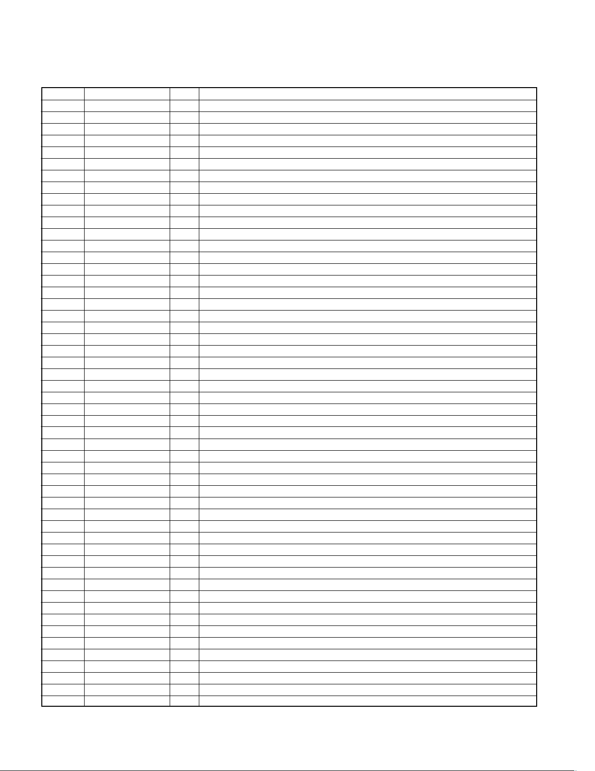
3. Microprocessor pin description (X32, IC6) :UPD784217GF501
Pin No. Pin Name I/O Description
1 A16(1M) O No used.
2 A17 O No connection.
3 SCL O No connection.
4 SDA I/O No connection.
5 RD O SRAM read strobe.
6 WR O SRAM write strobe
7 CE O Chip selector
8 ASTB(CE) O No connection.
9 VDD - Power supply(+5V).
10 RMUTE O Analog muting signal output.
11 RWRR O No connection.
12 RWR I No connection.
13 RTRN I No connection.
14-21 L-D7-D0 O No connection.
22 VPP - GND.
23 +5VPWM O Disc sensor ON/OFF. L:on
24 R-M-CW O Mechanism rotary motor(+). H:CCW
25 R-M-CCW O Mechanism rotary motor(-). H:CW
26 MON O Control port of poor focus works.
27 S3-SW I Mechanism address detector switch.
28 S2-SW I Mechanism address detector switch.
29 REG-ON O Power ON/OFF control.
30 LOADM- (IN2) O Loading motor(-) for main pickup.
31 LOADM+ (IN1) O Loading motor(+) for main pickup.
32 LDC O Laser on/off. L: Laser diode on.
33 SCLK O Sens serial data read clock.
34 SENS I SENS signal input.
35 CLK O Serial data clock.
36 XLAT O CXD2587Q latch. H î L:latch
37 VDD - Power supply(+5V).
38,39 X1,2 - Main system clock(12.5MHz).
40 VSS - GND.
41 XT2 - No connection.
42 XT1 I GND.
43 RESET I System reset signal input.
44 DATA O Serial data output.
45 MUTEG(SYSTEM) O System muting control output.
46 SCOR I Sub code synchro detection.
47 POWER I Power key input terminal.
48 REM I Remote control signal input.
49 SBUSY I/O Serial busy signal I/O.
50 SDATA I/O Serial data signal I/O.
51 AVDD - Power supply(+5V).
52 AVREF - A/D reference power supply.
53 PROTECT I Detection signal input of protection.
54 UNLOAD-SW1 I Unloading switch for main pickup.
55 LOAD-SW1 I Loading switch for main pickup.
56 S1-SW I Mechanism address detector switch.
57 DISC-SW2 I Disc2 sensor input..
58 DISC-SW I Disc sensor.
59 JOG2 I Encoder signal input.
60 JOG1 I Encoder signal input.
4
CD-425M/4260M/4700M/DPF-J6030
CIRCUIT DESCRIPTION
Pin No. Pin Name I/O Description
61 AVSS - GND.
62 LED O STANDBY LED control terminal.
63 ICRESET O IC reset.
64 AVREF1 - D/A reference power supply.
65 RXD-232C I No connection.
66 TXD-232C O No connection.
67 SQCK/SCK-SW O SQCK,SCK(DOT/DSP clock) selector. L:DSP.
68 RXD-R I No connection.
69 TXD-R O No connection.
70 DOOR-SW I Door open/close detector switch.
71 STB1 O Strobe signal output to dot driver.
72 S1 O Data output to dot driver.
73 SQS1 I Sub code read data input.
74 S0 I Data input from dot driver.
75 SCK/SQCK O Dot driver/sub code read clock.
76-83 A0~A7 O Address output to SRAM.
84-91 D0-7 I/O SRAM data bus.
92-98 A8~A14 O Address output to SRAM.
99 A15(1M) O No used.
100 VSS - GND.
4. FL Microprocessor : UPD 780232GC-012 (X32-IC13)
Pin description
Pin No. Pin Name I/O Description
1 VDD - Power supply(+5V)
2 VSS - GND.
3,4 X1,2 - Main system clock.(5MHz).
5 VPP - GND.
6 RESET I System reset input.
7 SCK I Serial clock.
8 SI I Data input.
9 SO O Data output.
10 POW-P I/O Timer sw on input. .
11 LED-A O No used.
12 LED-B O No used.
13 STANDBY O No used.
14 NC - No used.
15 STB I Strobe signal input.
16 REM I No used.
17 NC - No used.
18 AVSS - GND.
19,20 A/D3,A/D2 - GND.
21,22 A/D1,A/D0 I Key return signal input(1,0).
23 VSS - GND.
24,25 AVDD/VDD - Power supply(+5V)
26 NC - No connection.
27-43 P1-P17 O FL control output. 1G(38),2G-16G(P1to P17).
44-58 P21-35 O FL control output. 2G-16G(P21to P35).
59 VDD - Power supply(+5V)
60 VLOAD - Negative power supply(-37.5V)
61-63 P18-P20 O FL control output. 2G-16G(P18 to P20).
64 NC - No connection.
65-72 1G-8G O FL control output.1G-8G.
73-80 9G-16G O FL control output.9G-16G.
5
CD-425M/4260M/4700M/DPF-J6030
CIRCUIT DESCRIPTION
5. Test mode
INPUT KEY PROCEDURE DISPLAY
Insert the AC plug to INITIAL CONDITION MECHA. INITIAL
the wall outlet with • Disc No.1 moves to the center. INITIAL OK!!
pressing the SKIP- • Clear the memory of the SRAM.
DOWN key. • Door opens. INITIAL NG
• Set the switch of TIMER ON PLAY to ON. TIMER, NG
• Set the switch of SYSTEM CONTROL to XS8. SER, NG
Insert the AC plug to CIRCUIT ADJUSTMENT TEST ON
the wall outlet with • Open the door and load the disc to the Disc No.1.
pressing the REPEAT • Close the door. The unit changes to test mode 05 .
key after clamping the disc
PLAY/PAUSE Change the mode 05(tracking-on) and 03(tracking-off) alternately . 05 XX:XX 03 XX:XX
by the PLAY key
STOP Stop the function. 00
UP The pickup travels outwards. MOTOR FORWARD
DOWN The pickup travels inwards. MOTOR REVERSE
RANDOM Shows the result of self-adjustment.
07 EF/FB 07 XXX:XXX
08 TG/FG 08 XXX:XXX
09 FE/RF 09 XXX:XXX
10 TE/VC 10 XXX:XXX
Mode changes alternately by the RANDOM key. NG: blinking
REPEAT Playback PGM signal of the Track No.7,13,23,30,34
and 41 in the order. And release the test mode.
CONFIRM Release the test mode.
(TIMER PLAY SW) Check the switch position. TIMER ON , TIMER OFF
Insert the AC plug CHECK THE MECHANISM JAMMING.
to the wall outlet with Clamp the Disc No1,2,100,50,200 and 199 in the order.
pressing the UP key.
Insert the AC plug THE MECHANISM TEST MODE.
to the wall outlet with Display shows Niagara until pressing any keys.
pressing the
RANDOM key.
PLAY/PAUSE Change the mode 05(tracking-on) and 03(tracking-off) alternately 05 XX:XX 03X:XX
by the PLAY key.
STOP Stop the function.
Shows the result of self-adjustment.
07 EF/FB 07 XXX:XXX
08 TG/FG 08 XXX:XXX
09 FE/RF 09 XXX:XXX
10 TE/VC 10 XXX:XXX
Mode changes alternately by the STOP key. NG: blinking
UP Arm Motor Load operation. MOTOR LOAD
DOWN Arm Motor Unload operation. MOTOR UNLOAD
RANDOM Rotary Motor Clockwise turning. MOTOR CW
DISPLAY Rotary Motor Counterclockwise turning. MOTOR CCW
REPEAT Playback PGM signal of the Track No.1,23 and 41
in the order.And release the test mode.
CONFIRM Release the test mode.
(TIMER PLAY SW) Check the switch position. TIMER ON , TIMER OFF
6
 Loading...