


DP-1100
B
NOTE:
Please
has
all
KENWOOD
COMPACT
replace this
descriptions
service
manual
with
for DP-1100 and DP-110011.
the old DP-1100's manual (B51-1592-00).
DISC
DP-1100II
PLAYER
This
manual
Photo is DP-1100B
•Refer to Parts List on page 177.
TRIO-KENWOOD
equipment conforms to DHHS
tions
No. 21 CFR 1040.10, Chapter I,
Subchapter
DANGER:
and interlock defeated.
AVOID
DIRECT
Corp.
certifies this
J.
Laser
radiation when open
EXPOSURE
TO
Photo is DP-110011
'Refer to Parts List on page 191,
Regula-
BEAM.
DP-1100B
II
MEANING OF
ABBREVIATIONS
AFC:
Disc motor speed control signal output from IC8 on
process PCB
APC:
Disc motor phase control signal output from IC8 on
process PCB
BCK:
Clock pulse on which music data is sent to D/A
con-
verter (Bit clock pulse)
CK4M:
Clock signal of about 4 MHz for microprocessor (the
signal resultant from 1/2 frequency division of X'tal
OSC 8.4672 MHz)
CK88:
About 88 kHz signal which is identical with signal
WDCK (word clock pulse) output from IC6 on pro-
cess PCB. It is used as clock signal for IC15 on servo
PCB or as pseudo EFM signal.
CLS:
Switch to inform opened or closed tray state. It is
shorted with tray closed. ("L" with tray closed)
CLV:
Circuit which makes the linear velocity of disc motor
constant to provide constant reading rate of disc
data.
DATA
12 and DATA 21: Signals for data communication
(transmission and reception) between CPU 1 and
CPU 2.
DATA:
Signal line on which data is sent from process PCB
to D/A converter.
DCON:
Signal which is output from Id 5 on servo PCB. It is
normally "H" and becomes "L" when RF signal is
lowered in level due to disc flaw. (Dropout control)
DIN: Signal line on which positional data of disc flaw is
transmitted between disc flaw position memory cir-
cuit and IC15 on servo PCB.
DISK:
Disc motor drive signal
DOCK:
Clock pulse output from IC15 on servo PCB to disc
flaw position memory circuit. It is a six times
amplified signal of FGS. (Dropout clock pulse)
DOK:
With disc provided, this pulse output is "L". Q1 on
servo PCB detects the presence or absence of disc.
(Disc OK)
DSG:
Refer to "IC15 pin function" on page 68.
EFM,
EFM 1 and EFM 0: Eight-to-Fourteen-Modulation
signals. These are high-frequency signals or RF
signals given from optical pickup.
EMPH:
Pre-emphasis signal output from IC8 on process
PCB.
F.COIL
and
T.COIL:
Focusing and tracking coils control
signals.
FE
or F.E: Focus error signal
FG4:
Signal resultant from 1/30 frequency division of
signal DOCK. It controls disc motor drive signal.
FGS:
IC15 input pin of FG signal from disc motor.
FOK:
Focus servo control signal. Servo ON with signal
FOK "L".
FOKG:
Refer to "IC15 pin function" on page 69.
FSRH
or
FSRCH:
2 Hz signal to detect just focusing point. It
moves the pickup actuator up and down.
IRQ:
Interrupt control I/O pin between CPU 1 and CPU 2
(Interrupt request)
KGC:
Inversion signal of signal RFG in IC15. It is normally
"L"
and "H" during kick of motor.
KICFB
or
KCIF:
Refer to "IC15 pin function" on page 70.
LDC:
Refer to "IC15 pin function" on page 69.
LRCK:
Signal output from IC6 on process PCB. It indicates
whether output data is for L-ch or R-ch.
MODE 4: IC15 control signal which is output from main
CPU.
(Refer to page 70.)
M5P: Disc motor ON/OFF control signal.
MUTE:
Music signal muting signal.
OPEN:
Switch which turns ON ("L") with tray open to in-
form opened tray state.
OPNS:
Refer to "IC15 pin function" on page 68.
PLAY:
Refer to "IC15 pin function" on page 69.
PLCK:
Refer to "IC15 pin function" on page 71.
PU
or P.U: Pickup.
PUD:
Refer to "IC15 pin function" on page 68.
PUFB:
Inversion signal of signal PUFF in IC15.
RES:
CPU initialize signal
RFES:
Refer to "IC15 pin function" on page 69.
RFG:
Refer to "IC15 pin function" on page 70.
RFOK:
This output becomes "L" when RF signal from
pickup is input to IC10 (V2).
RMC:
Output signal from remote control signal amplifier
S1 and S2: Pickup output signals emitted from preamplifier
on mechanism PCB.
SCK:
Clock pulse for communication between CPU1 and
CPU 2. (Serial clock pulse)
SLT:
Switch which turns ON ("L") with pickup at inner-
most track.
START
or
STAT:
IC12 control signal to enable SVC opera
tion by main CPU. (IC12 ON at "H")
SVC
(A, B, C and INH): Servo control
TE
or T.E: Tracking error signal or tracking monitor pin
TEG
1 and TEG 2: Refer to "IC15 pin function" on page
68.
TEOP
and
TEON:
Refer to "IC15 pin function" on page 68.
TEP:
Refer to "IC15 pin function" on page 68.
TES:
Refer to "IC15 pin function" on page 68.
TRAY
or TRY: Disc tray or tray drive signal
TTAC:
Refer to "IC15 pin function" on page 68.
WDCK:
Signal output from IC6 on process PCB. Its fre
quency is twice that of signal LRCK.
5
DP-1100B
II
DP-1100B
II
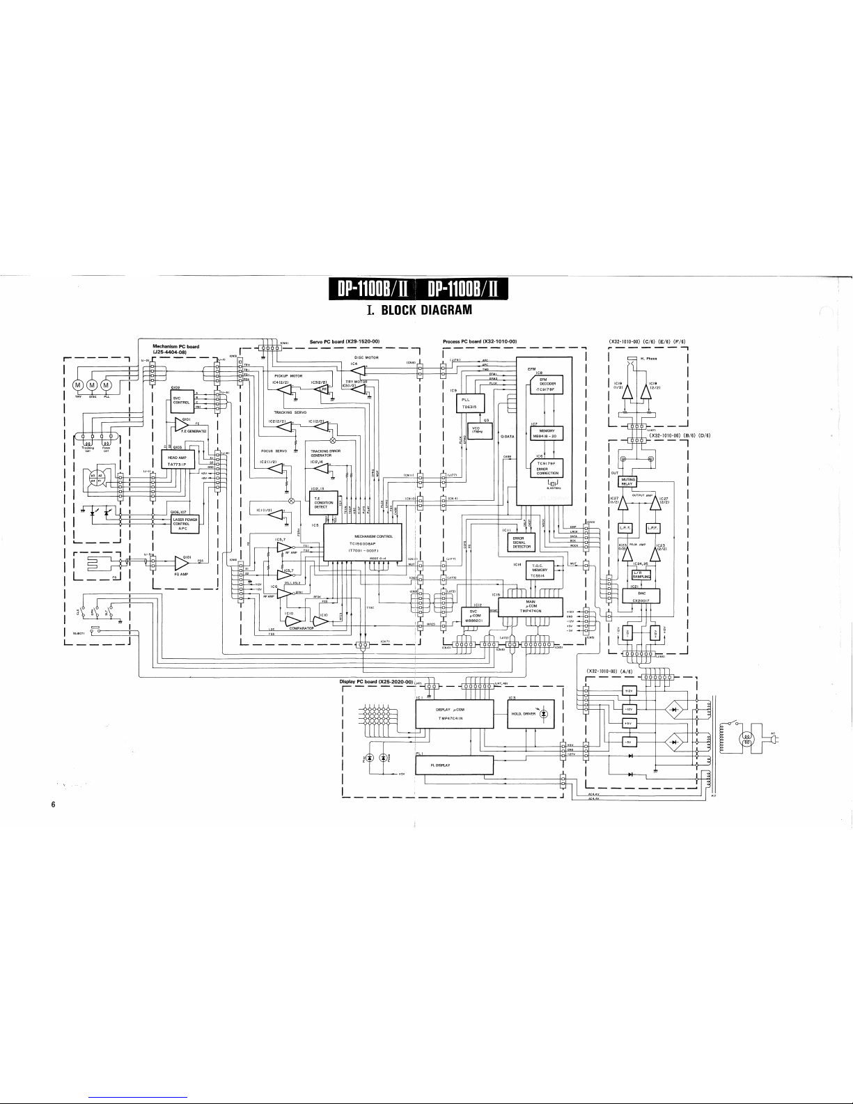
I.
BLOCK
DIAGRAM
DP-1100B
II
II.
FUNDAMENTALS
1 FUNDAMENTALS
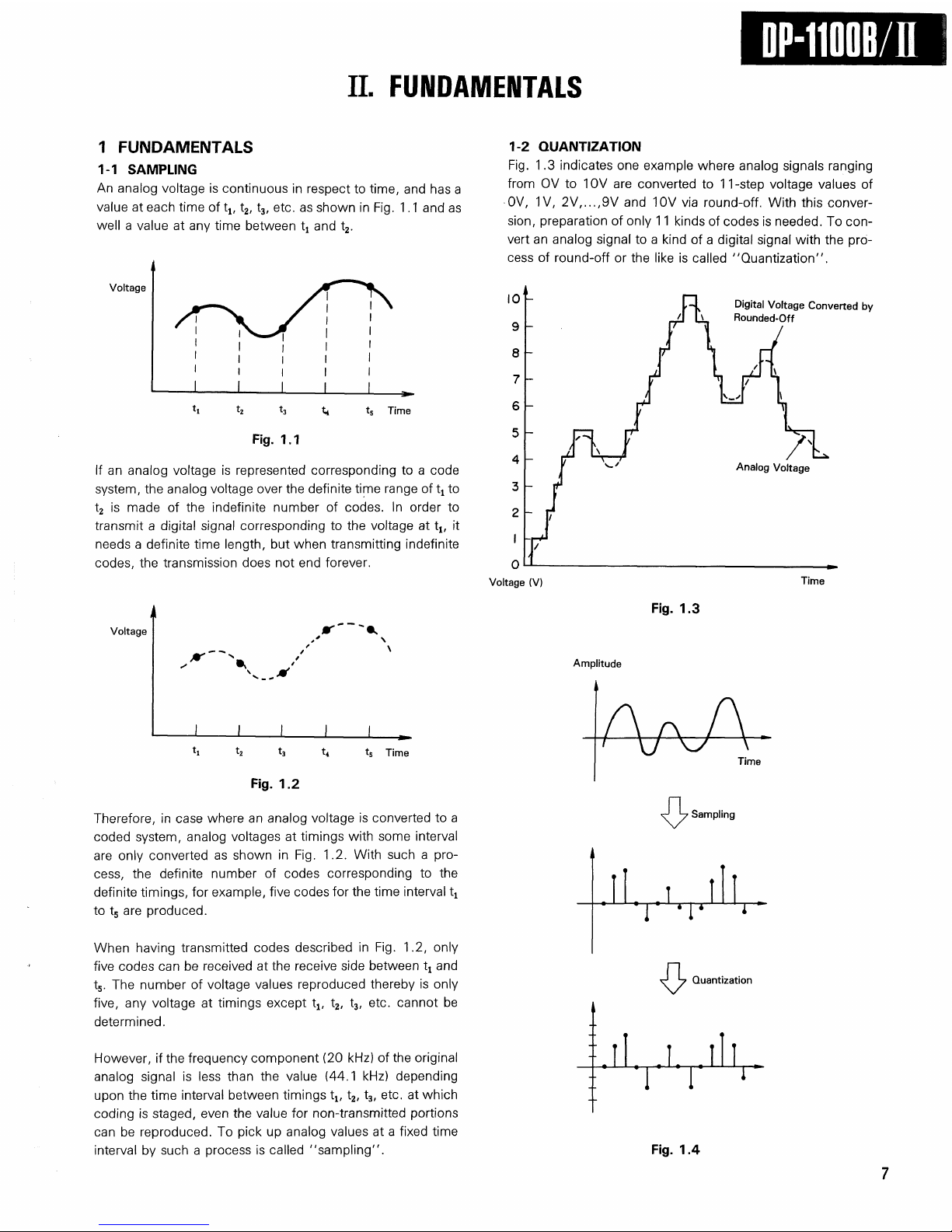
1-1 SAMPLING
An analog voltage is continuous in respect to time, and has a
value at each time of t1( t2, t3, etc. as shown in Fig. 1.1 and as
well a value at any time between tx and t2.
Voltage
Time
If an analog voltage is represented corresponding to a code
system,
the analog voltage over the definite time range of tt to
t2 is made of the indefinite number of codes. In order to
transmit a digital signal corresponding to the voltage at t1( it
needs a definite time length, but when transmitting indefinite
codes, the transmission does not end forever.
Voltage
t5 Time
Fig.
1.2
Therefore, in case where an analog voltage is converted to a
coded system, analog voltages at timings with some interval
are only converted as shown in Fig. 1.2. With such a pro-
cess,
the definite number of codes corresponding to the
definite timings, for example, five codes for the time interval t
t
to t5 are produced.
When having transmitted codes described in Fig. 1.2, only
five codes can be received at the receive side between tt and
t5. The number of voltage values reproduced thereby is only
five,
any voltage at timings except t1( t2, t3, etc. cannot be
determined.
However, if the frequency component (20 kHz) of the original
analog signal is less than the value (44.1 kHz) depending
upon the time interval between timings t1( t2, t3, etc. at which
coding is staged, even the value for non-transmitted portions
can be reproduced. To pick up analog values at a fixed time
interval by such a process is called "sampling".
1-2 QUANTIZATION
Fig.
1.3 indicates one example where analog signals ranging
from OV to 10V are converted to 11-step voltage values of
0V, 1V, 2V 9V and 10V via round-off. With this conver-
sion,
preparation of only 11 kinds of codes is needed. To
con-
vert an analog signal to a kind of a digital signal with the pro-
cess of round-off or the like is called "Quantization".
Digital
Voltage Converted by
Rounded-Off
Time
Fig.
1.3
Amplitude
Sampling
Quantization
Fig.
1.4
Analog Voltage
Voltage (V)
Fig.
1.1
DP-1100B
II
II.
FUNDAMENTALS
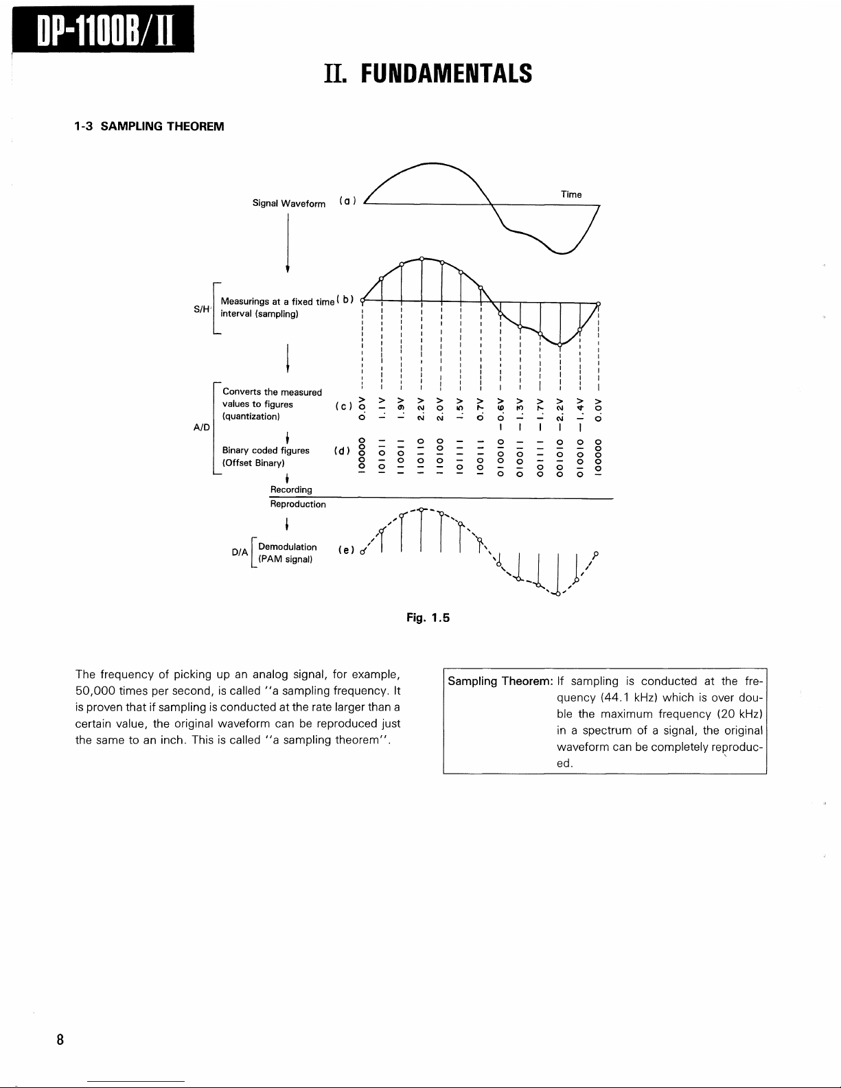
1-3 SAMPLING
THEOREM
Signal
Waveform (a )
S/H
;
Measurings
at a fixed
time
( b)
interval (sampling)
A/D
Converts
the measured
values
to figures
(quantization)
f
Binary
coded figures
(Offset Binary)
D/A
Reproduction
Demodulation
(PAM signal)
Fig.
1.5
The frequency of picking up an analog signal, for example,
50,000 times per second, is called "a sampling frequency. It
is proven that if sampling is conducted at the rate larger than a
certain value, the original waveform can be reproduced just
the same to an inch. This is called "a sampling theorem".
Sampling
Theorem: If sampling is conducted at the fre-
quency (44.1 kHz) which is over dou-
ble the maximum frequency (20 kHz)
in a spectrum of a signal, the original
waveform can be completely reproduc-
ed.
8
Recording
DP-1100B
II
II.
FUNDAMENTALS
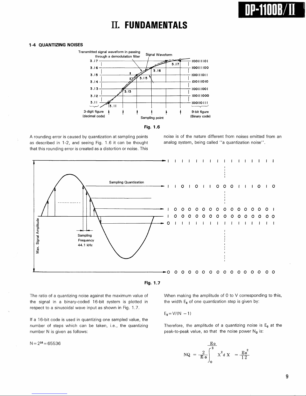
1-4 QUANTIZING
NOISES
Transmitted
signal
waveform in
passing
through a demodulation
filter
Signal
Waveform
3-digit
figure
(decimal code)
Sampling
point
9-bit
figure
(Binary
code)
A rounding error is caused by quantization at sampling points
as described in 1-2, and seeing Fig. 1.6 it can be thought
that this rounding error is created as a distortion or noise. This
noise is of the nature different from noises emitted from an
analog system, being called "a quantization noise".
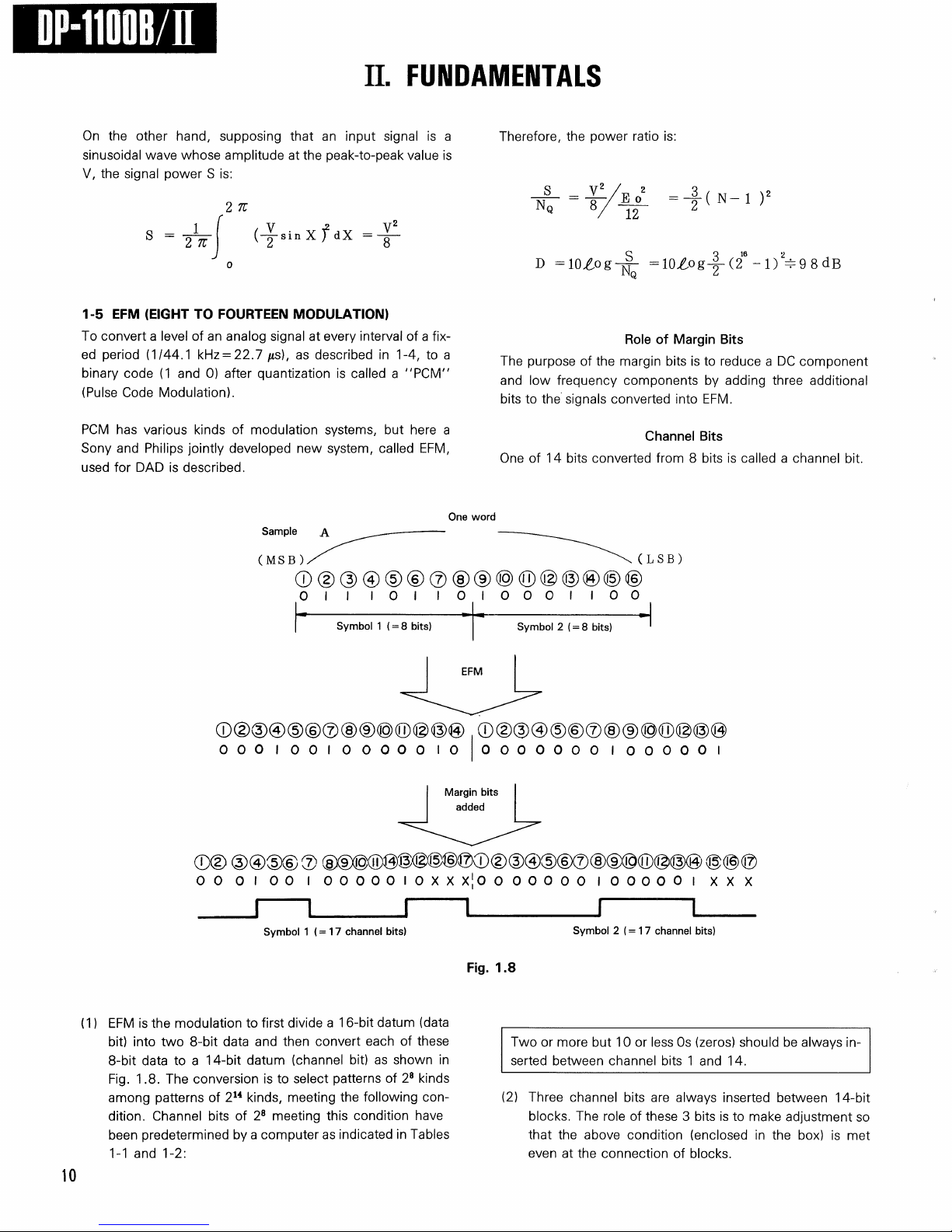
The ratio of a quantizing noise against the maximum value of
the signal in a binary-coded 16-bit system is plotted in
respect to a sinusoidal wave input as shown in Fig. 1.7.
If a 16-bit code is used in quantizing one sampled value, the
number of steps which can be taken, i.e., the quantizing
number N is given as follows:
When making the amplitude of 0 to V corresponding to this,
the width E0 of one quantization step is given by:
E0 = V/(N -1)
Therefore, the amplitude of a quantizing noise is E0 at the
peak-to-peak value, so that the noise power NQ is:
N = 216 = 65536
Fig.
1.6
Sampling
Quantization
Sampling
Frequency
44.1 kHz
Max.
Signal
Amplitude
Fig.
1.7
9
DP-1100B
II
II.
FUNDAMENTALS
On the other hand, supposing that an input signal is a
sinusoidal wave whose amplitude at the peak-to-peak value is
V, the signal power S is:
1-5 EFM (EIGHT TO
To convert a level of an analog signal at every interval of a fix-
ed period (1/44.1 kHz = 22.7 /is), as described in 1-4, to a
binary code (1 and 0) after quantization is called a "PCM"
(Pulse Code Modulation).
PCM has various kinds of modulation systems, but here a
Sony and Philips jointly developed new system, called EFM,
used for DAD is described.
FOURTEEN
Sample
MSB
MODULATION)
A
One
Therefore, the power ratio is:
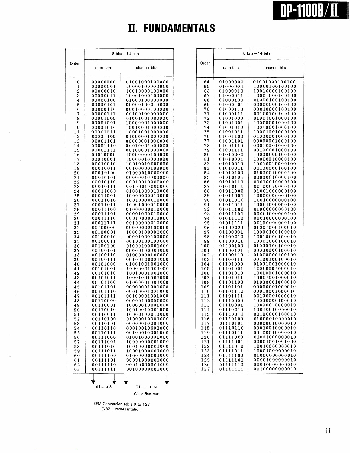
Role
of
Margin
The purpose of the margin bits is to reduce a DC component
and low frequency components by adding three additional
bits to the signals converted into EFM.
Channel
One of 14 bits converted from 8 bits is called a channel bit.
word
LSB
Bits
Bits
Symbol
1 (= 8 bits)
Symbol
1 (= 17 channel bits)
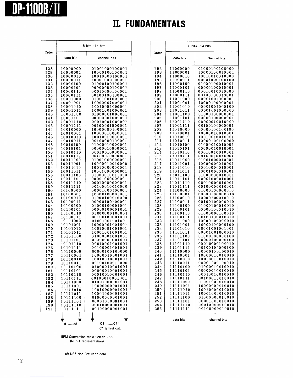
(1)
EFM is the modulation to first divide a 16-bit datum (data
bit)
into two
8-bit
data to a 14-bit datum (channel bit) as shown in
Fig.
1.8. The conversion is to select patterns of 28 kinds
among patterns of 214 kinds, meeting the following
dition.
been predetermined by a computer as indicated in Tables
1-1 and 1-2:
8-bit
data and then convert each of these
con-
Channel bits of 28 meeting this condition have
EFM
Margin
added
Symbol 2 (
bits
Fig.
1.8
Two or more but 10 or less Os (zeros) should be always in-
serted between channel bits 1 and 14.
(2)
Three channel bits are always inserted between 14-bit
= 8 bits)
Symbol
2 {= 17 channel bits)
blocks. The role of these 3 bits is to make adjustment so
that the above condition (enclosed in the box) is met
even at the connection of blocks.
II.
FUNDAMENTALS
DP-1100B
II
d1 d8
C1
C14
C1
is
first
cut.
EFM
Conversion
table
0 to 127
(NRZ-1
represantation)
8 bits-14 bits
Order
data bits
channel
bits
0
00000000
01001000100000
i
00000001
10000100000000
2
00000010
10010000100000
3
00000011
10001000100000
4
00000100
01000100000000
5
00000101
00000100010000
6
00000110
00010000100000
7
00000111
00100100000000
8
00001000
01001001000000
9
00001001
10000001000000
10
00001010
10010001000000
1 1
00001011
10001001000000
12
00001100
01000001000000
13
00001101
00000001000000
14
00001
110
00010001000000
15
00001
111
00100001000000
16
00010000
10000000100000
17
00010001
10000010000000
18
00010010
10010010000000
19
00010011
00100000100000
20
00010100
01000010000000
21
00010101
00000010000000
22
00010110
00010010000000
23
0001 01 11
00100010000000
24
00011000
01001000010000
25
00011001
10000000010000
26
00011010
10010000010000
27
00011011
10001000010000
28
00011 100
01000000010000
29
00011101
00001000010000
30
00011110
00010000010000
31
00011111
00100000010000
32
00100000
00000000100000
33
00100001
10000100001000
34
00100010
00001000100000
35
00100011
00100100100000
36
00100100
01000100001000
37
00100101
00000100001000
38
00100110
01000000100000
39
00100111
00100100001000
40
00101000
01001001001000
41
00101001
10000001001000
42
00101010
10010001001000
43
00101011
10001001001000
44
00101100
01000001001000
45
00101101
00000001001000
46
00101110
00010001001000
47
00101111
00100001001000
48
00110000
00000100000000
49
00110001
10000010001000
50
00110010
10010010001000
51
00110011
10000100010000
52
00110100
01000010001000
53
00110101
00000010001000
54
00110110
00010010001000
55
00110111
00100010001000
56
00111000
01001000001000
57
00111001
10000000001000
58
00111010
10010000001000
59
00111011
10001000001000
60
00111100
01000000001000
61
00111101
00001000001000
62
00111110
00010000001000
63
00111111
00100000001000
8 bits -14 bits
Order
data bits
channel
bits
64
01000000
01001000100100
65
01000001
10000100100100
66
01000010
10010000100100
67
01000011
10001000100100
68
01000100
01000100100100
69
01000101
00000000100100
70
01000110
00010000100100
71
01000111
00100100100100
72
01001000
01001001000100
73
01001001
10000001000100
74
01001010
10010001000100
75
01001011
10001001000100
76
01001100
01000001000100
77
01001101
00000001000100
78
01001110
00010001000100
79
01001111
00100001000100
80
01010000
10000000100100
81
01010001
10000010000100
82
01010010
10010010000100
83
01010011
00100000100100
84
01010100
01000010000100
85
01010101
00000010000100
86
01010110
00010010000100
87
01010111
00100010000100
88
01011000
01001000000100
89
01011001
10000000000100
90
01011010
10010000000100
91
01011011
10001000000100
92
0101 1100
01000000000100
93
01011101
00001000000100
94
01011110
00010000000100
95
01011111
00100000000100
96
01100000
01001000100010
97
01100001
10000100100010
98
01100010
10010000100010
99
01100011
10001000100010
100
01100100
01000100100010
101
01100101
00000000100010
102
01100110
01000000100100
103
01100111
00100100100010
104
01101000
01001001000010
105
01101001
10000001000.010
106
01101010
10010001000010
107
01101011
10001001000010
108
01101100
01000001000010
109
01101101
00000001000010
110
01101110
00010001000010
111
01101111
00100001000010
112
01110000
10000000100010
113
01110001
10000010000010
114
Oil
10010
10010010000010
115
Oil
10011
00100000100010
116
Oil
10100
01000010000010
117
01110101
00000010000010
1 18
01110110
00010010000010
119
01110111
00100010000010
120
011110
00
01001000000010
121
01111001
00001001001000
122 01
111010
10010000000010
123
01111011
10001000000010
124
01111100
01000000000010
125
01111101
00001000000010
126
01111110
00010000000010
127
01111111
00100000000010
DP-1100B
II
II.
FUNDAMENTALS
d1 d8
C1
C14
C1
is
first
cut.
data bits
channel
bits
EFM
Conversion
table
128 to 255
(NRZ-1
represantation)
cf:
NRZ Non
Return
to
Zero
Order
8 bits —
14
bits
Order
data bits
channel
bits
128 10000000
01001000100001
129
10000001
10000100100001
130
10000010
10010000100001
131
10000011
10001000100001
132 10000100
01000100100001
133
10000101
00000000100001
134
100001
10
00010000100001
135
10000111
00100100100001
136 10001000
01001001000001
137
10001001
10000001000001
138 10001010
10010001000001
139
10001011
10001001000001
140 10001100
01000001000001
141
10001101
00000001000001
142 10001110
00010001000001
143
10001111
00100001000001
144 10010000
10000000100001
145
10010001
10000010000001
146 10010010
10010010000001
147
10010011
00100000100001
148
10010100
01000010000001
149
10010101
00000010000001
150
10010110
00010010000001
151
10010111
00100010000001
152
10011000
01001000000001
153
10011001
10000010010000
154
1001 1010
10010000000001
155
10011011
10001000000001
156 1001 1100
01000010010000
157
10011101
00001000000001
158
10011110
00010000000001
159
10011111
00100010010000
160
10100000
00001000100001
161
10100001
10000100001001
162
10100010 01000100010000
163
10100011
00000100100001
164
10100100
01000100001001
165
10100101
00000100001001
166
10100110 0100
0000100001
167
10100111
00100100001001
168 1010 1000
01001001001001
169
10101001
10000001001001
170 10101010
10010001001001
171
10101011
10001001001001
172
10101100
01000001001001
173
10101101
00000001001001
174
10101110
00010001001001
175
1010111
1
00100001001001
176
10110000
00000100100000
177
10110001
10000010001001
178
101 10010
10010010001001
179
10110011
00100100010000
180
10110100
01000010001001
181
10110101
00000010001001
182
10110110
00010010001001
183
10110111
00100010001001
184
10111000
01001000001001
185
10111001
10000000001001
186
10111010
10010000001001
187
10111011
10001000001001
188
10111100
01000000001001
189
10111101
00001000001001
190
10111110
00010000001001
191
10111111
00100000001001
Order
8 bits —
14
bits
Order
data bits
channel
bits
192 11000000 01000100100000
193
11000001
10000100010001
194
11000010 10010010010000
195
11000011
00001000100100
196
11000100
01000100010001
197
11000101
00000100010001
198
11000110
00010010010000
199
11000111
00100100010001
200
11001000
00001001000001
201
11001001
10000100000001
202 11001010
00001001000100
203
11001011
00001001000000
204 11001100
01000100000001
205
11001101
00000100000001
206 11001110 00000010010000
207
11001111
00100100000001
208
11010000 00000100100100
209
11010001
10000010010001
210 11010010
10010010010001
211
11010011
10000100100000
212 11010100
01000010010001
213
11010101
00000010010001
21*4
110101
10
00010010010001
215
11010111
00100010010001
216
11011000
01001000010001
217
11011001
10000000010001
218 11011010
10010000010001
219
11011011
10001000010001
220
11011100
01000000010001
221
11011101
00001000010001
222 11011110
00010000010001
223
11011111
00100000010001
224
11100000 01000100000010
225
11100001
00000100000010
226
11100010
10000100010010
227 11
100011
00100100000010
228
11100100 01000100010010
229
11100101
00000100010010
230
11100110 01000000100010
231
1
1100111
00100100010010
232
11101000 10000100000010
233
11101001
10000100000100
234 11101010
00001001001001
235
11101011
00001001000010
236 11101100 01000100000100
237
11101101
00000100000100
238
11101110
00010000100010
239
111011
11 00100100000100
240
11110000 00000100100010
241
11110001
10000010010010
242
11 110010
10010010010010
243
11110011
00001000100010
244
111 10100
01000010010010
245 1
1110101
00000010010010
246 11110110
00010010010010
247
111 10111
00100010010010
248 111 11000 01001000010010
249
111 11001 10000000010010
250 11111010
10010000010010
251
11111011
10001000010010
252
111 11100 01000000010010
253
11111101
00001000010010
254 11111110
00010000010010
255
11111111
00100000010010
II.
FUNDAMENTALS
DP-1100B
II
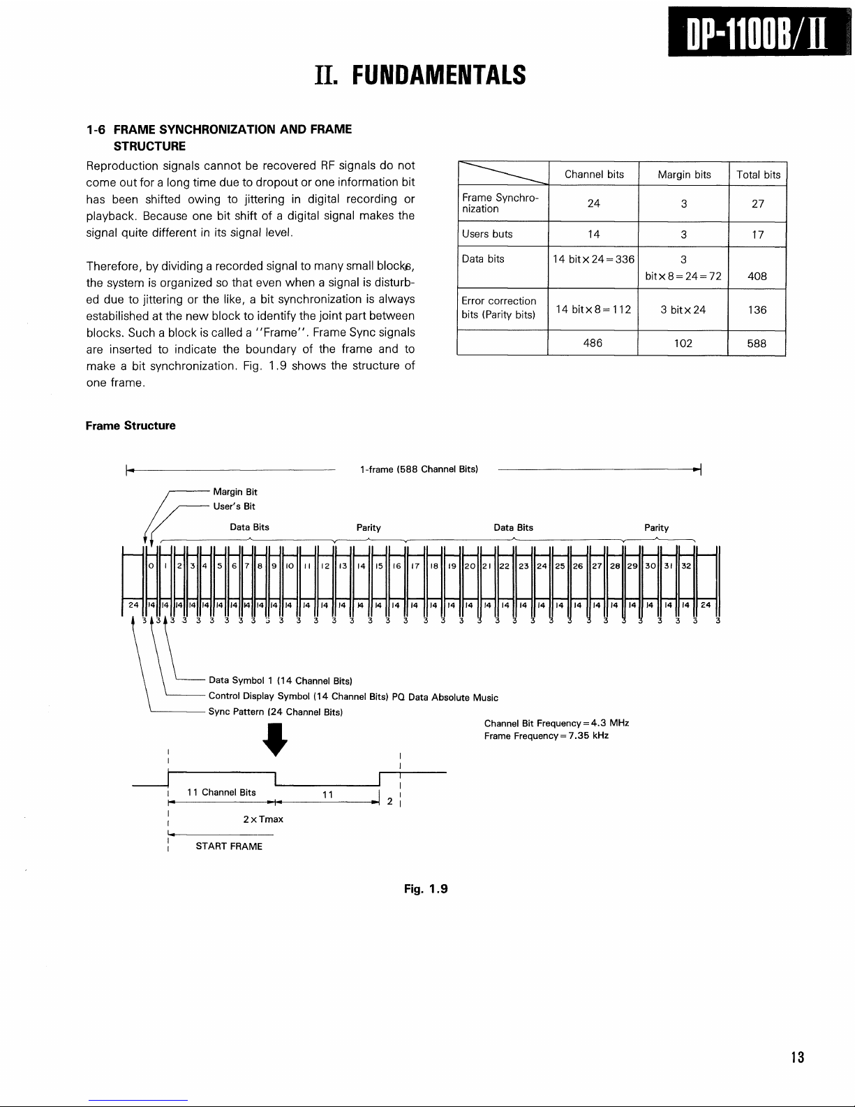
1-6
FRAME
SYNCHRONIZATION AND
FRAME
STRUCTURE
Reproduction signals cannot be recovered RF signals do not
come out for a long time due to dropout or one information bit
has been shifted owing to jittering in digital recording or
playback. Because one bit shift of a digital signal makes the
signal quite different in its signal level.
Therefore, by dividing a recorded signal to many small blockjs,
the system is organized so that even when a signal is disturb-
ed due to jittering or the like, a bit synchronization is always
estabilished at the new block to identify the joint part between
blocks. Such a block is called a "Frame". Frame Sync signals
are inserted to indicate the boundary of the frame and to
make a bit synchronization. Fig. 1.9 shows the structure of
one frame.
Channel bits
Margin bits
Total bits
Frame Synchro-
nization
24
3
27
Users buts
14
3
17
Data bits
14 bitx24 = 336
3
bitx8 = 24 = 72
408
Error correction
bits (Parity bits)
14 bitx8=112
3 bit x 24
136
486
102 588
Frame
Structure
1-frame
(588 Channel
Bits)
Data
Bits
Parity Data
Bits
Parity
I
2 3 4 5 6 7 8 9 10
11 12
13
14 15
16
17 18 19 20 21
22
23 24
25
26 27 28 29 30
31
32
14 14 14 14 14 14
14
14 14 14
14 14 14 14 14 14 14 14 14 14 14 14 14 14
14
14 14 14
14 14 14
24
3A
-3 : : :
. ;
: :
i
2
: :
. 2
:
:
i
:
i : ; :
Data Symbol 1 (14 Channel
Bits)
Control Display Symbol (14 Channel
Bits)
PQ Data Absolute Music
Sync
Pattern (24 Channel
Bits)
11 Channel
Bits
11
2
x Tmax
START
FRAME
Fig.
1.9
•
Margin
Bit
User's
Bit
Channel
Bit
Frequency
= 4.3 MHz
Frame
Frequency = 7.35 kHz
DP-1100B
1-7
COMPACT
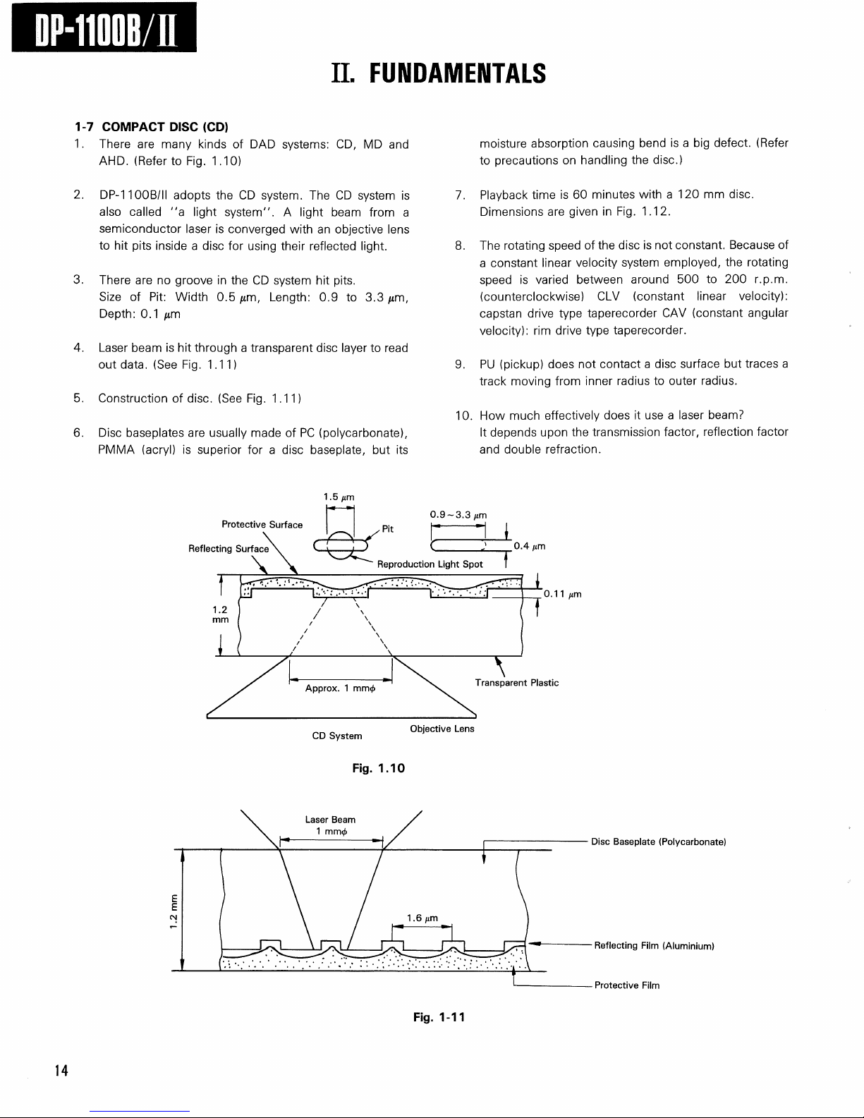
1.
There are many kinds of DAD systems: CD, MD and
AHD.
(Refer to Fig. 1.10)
II
DISC
(CD)
II.
FUNDAMENTALS
moisture absorption causing bend is a big defect. (Refer
to precautions on handling the disc.)
2.
DP-1100B/II adopts the CD system. The CD system is
also called "a light system". A light beam from a
semiconductor laser is converged with an objective lens
to hit pits inside a disc for using their reflected light.
3. There are no groove in the CD system hit pits.
Size of Pit: Width 0.5 fim, Length: 0.9 to 3.3 /im,
Depth:
0.1 /im
4.
Laser beam is hit through a transparent disc layer to read
out data. (See Fig. 1.11)
5. Construction of disc. (See Fig. 1.11)
6. Disc baseplates are usually made of PC (polycarbonate),
PMMA (acryl) is superior for a disc baseplate, but its
1.5 /tm
Reflecting
1.2
mm
Protective
Surface
Surface
Pit
Reproduction Light Spot
7. Playback time is 60 minutes with a 120 mm disc.
Dimensions are given in Fig. 1.12.
8. The rotating speed of the disc is not constant. Because of
a constant linear velocity system employed, the rotating
speed is varied between around 500 to 200 r.p.m.
(counterclockwise) CLV (constant linear velocity):
capstan drive type taperecorder CAV (constant angular
velocity):
9. PL) (pickup) does not contact a disc surface but traces a
track moving from inner radius to outer radius.
10.
How much effectively does it use a laser beam?
It depends upon the transmission factor, reflection factor
and double refraction.
0.9-3.3
nm
rim drive type taperecorder.
0.4
nm
0.11 nm
14
1.2 mm
Approx. 1 mm0
CD
System
Fig.
Laser
Beam
1 mm0
1.10
Objective
1.6 /tm
Fig.
1-11
Lens
Transparent
Plastic
Disc
Baseplate
Reflecting Film (Aluminium)
Protective Film
(Polycarbonate)
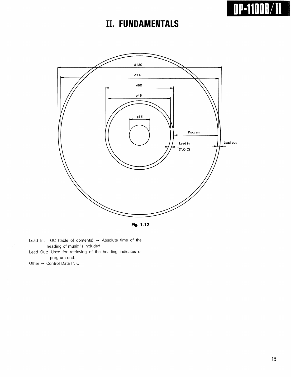
II.
FUNDAMENTALS
Lead
in
"(T.O.C)
Program
DP-1100B
Lead
out
II
Fig.
1.12
Lead In: TOC (table of contents) — Absolute time of the
heading of music is included.
Lead Out: Used for retrieving of the heading indicates of
program end.
Other — Control Data P, Q
15
DP-1100B
II
11.
100%
II.
FUNDAMENTALS
Reflection Film
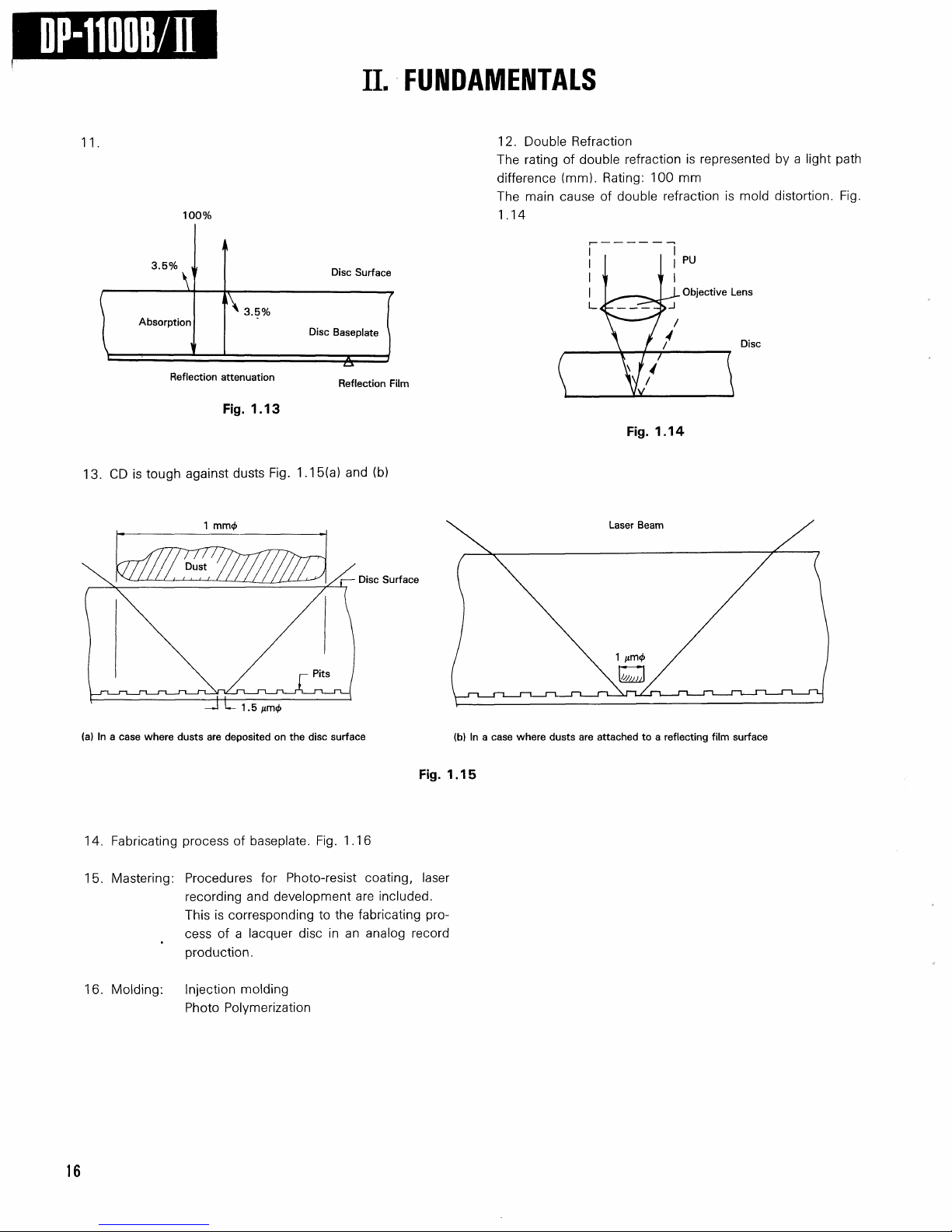
13.
CD is tough against dusts Fig.
1.15(a)
and (b)
12.
Double Refraction
The rating of double refraction is represented by a light path
difference (mm). Rating: 100 mm
The main cause of double refraction is mold distortion. Fig.
1.14
Disc
Fig.
1.14
1 mm#
Disc
Surface
14.
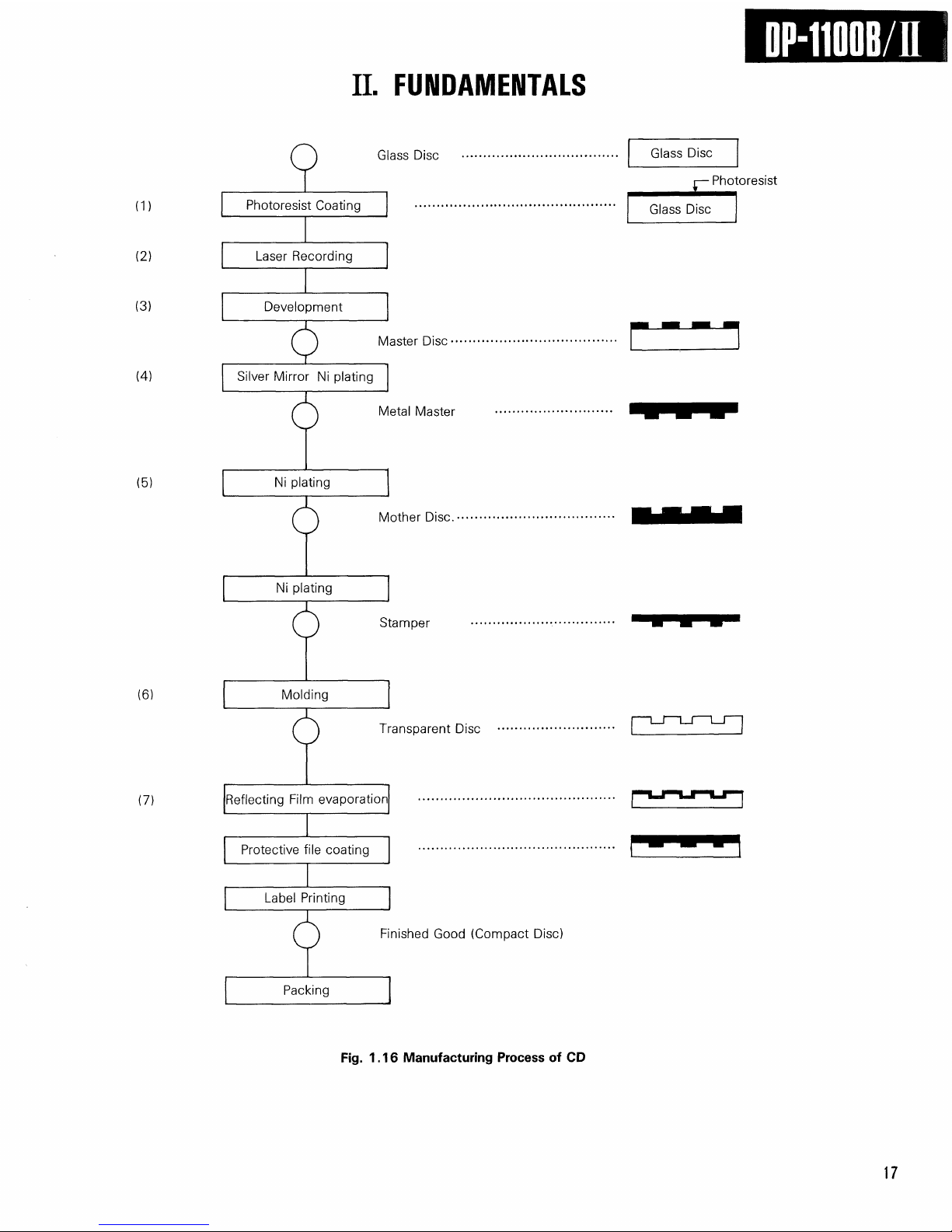
Fabricating process of baseplate. Fig. 1.16
15.
Mastering: Procedures for Photo-resist coating, laser
recording and development are included.
This is corresponding to the fabricating pro-
cess of a lacquer disc in an analog record
production.
16.
Molding: Injection molding
Photo Polymerization
6
Disc
Surface
Disc
Baseplate
Absorption
Reflection attenuation
Fig.
1.13
PU
. Objective
Lens
Dust
Pits
1.5
nm<j>
(a) In a
case
where
dusts
are deposited on the
disc
surface
Laser
Beam
1
iirr\<t>
(b) In a
case
where
dusts
are attached to a reflecting
film
surface
Fig.
1.15
II.
FUNDAMENTALS
0P-1100B II
Glass Disc
Photoresist Coating
Laser Recording
Development
Master Disc
•
Silver Mirror Ni plating
Metal Master
Ni plating
Mother Disc.
Ni plating
Stamper
Molding
Transparent Disc
Finished Good (Compact Disc)
Packing
Glass Disc
Photoresist
Glass Disc
Fig.
1.16
Manufacturing
Process
of CD
17
Reflecting Film evaporation
Protective file coating
Label Printing
DP-1100B II
II.
FUNDAMENTALS
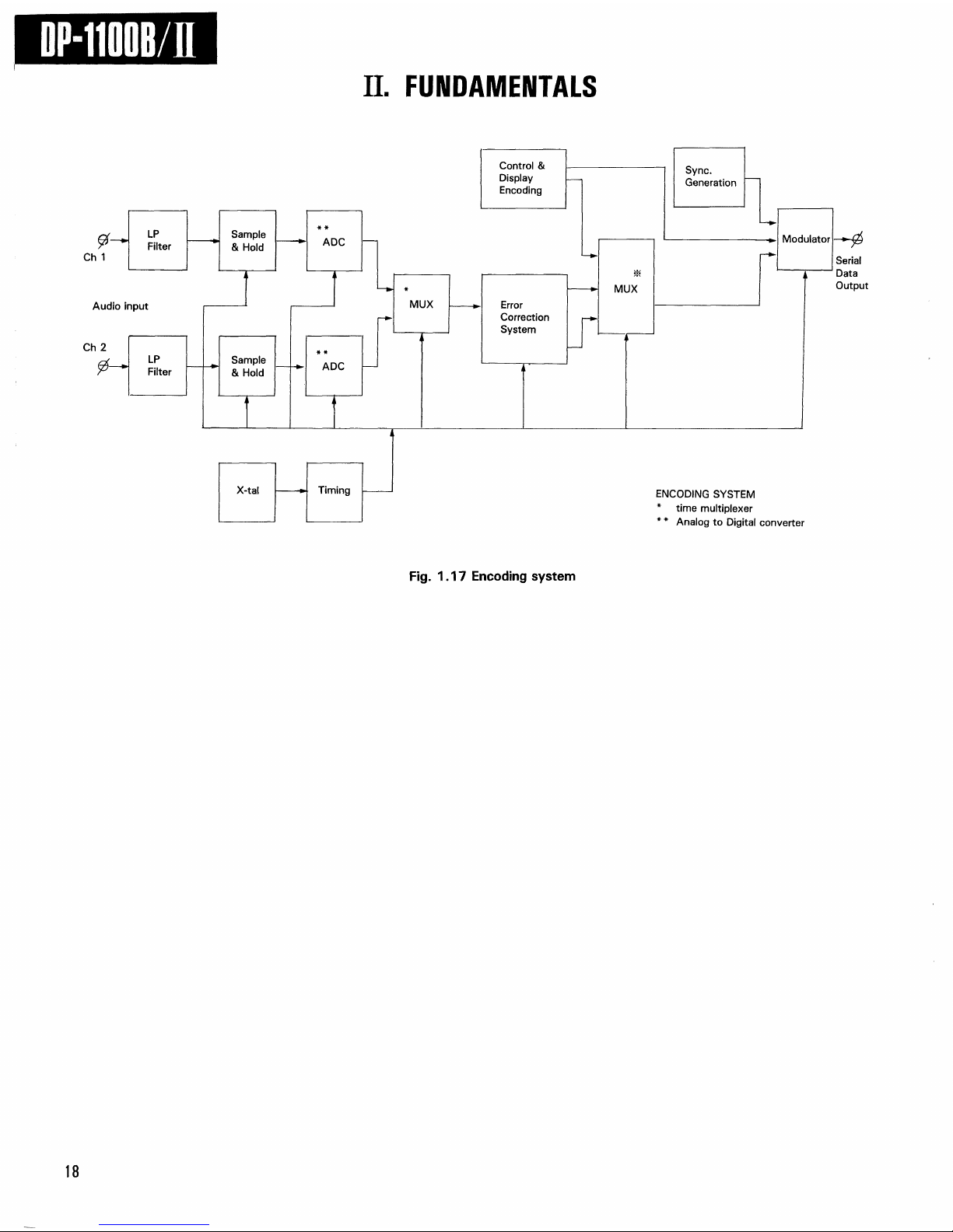
Audio input
Ch
2
LP
Filter
Sample
&
Hold
ADC
Control &
Display
Encoding
Error
Correction
System
Sync.
Generation
Modulator
Serial
Data
Output
X-tal
Timing
ENCODING
SYSTEM
*
time
multiplexer
* * Analog to
Digital
converter
Fig.
1.17 Encoding system
8
LP
Filter
Sample
&
Hold
ADC
Ch
1
MUX
MUX
DP-1100B
II
II.
FUNDAMENTALS
2
CODE
ERROR
2-1
CAUSES
OF
CODE
ERROR
(1)
Defectives which are already present on a disc at
delivery:
— Dusts attached to pits during production of disc.
— Disc molding distortion (entering of air bubbles whose
refraction factor is not equal.)
(2) Faults created on handling of a disc: dusts, scratches,
stains and finger prints.
(3)
Level variations of reproduction signal (eye pattern)
Because protection of out-of-tracking, Focus and CLV
are all depending on a servo system, poor stability of the
servo leads to increased code errors.
2-2 KINDS OF
CODE
ERROR
(1)
Random Error: an error which causes an error in one bit
(2) Burst Error: an error which causes an error in many suc-
cessive bits.
2-3
INTERLEAVE
Even if reading every page of a book slantwise from its upper
left side to lower right side, you can fully recognize the
con-
text or contents. However, you cannot recognize the contents
of the book if you are reading carefully one character or
clause without reading several tens of pages.
An error collection code is the same as this, and correction is
easy even when code errors of some bits are present.
However, if many, say 1000, bits are consecutively wrong at
a time, it is very difficult to correct those errors.
Therefore, the technique with which an order of a signal is
once changed and then recorded and, after reproduction,
returned back to the original order is employed. This changing
of the order of a signal is called an "interleave", and the
returning to the original order is called a "deinterleave".
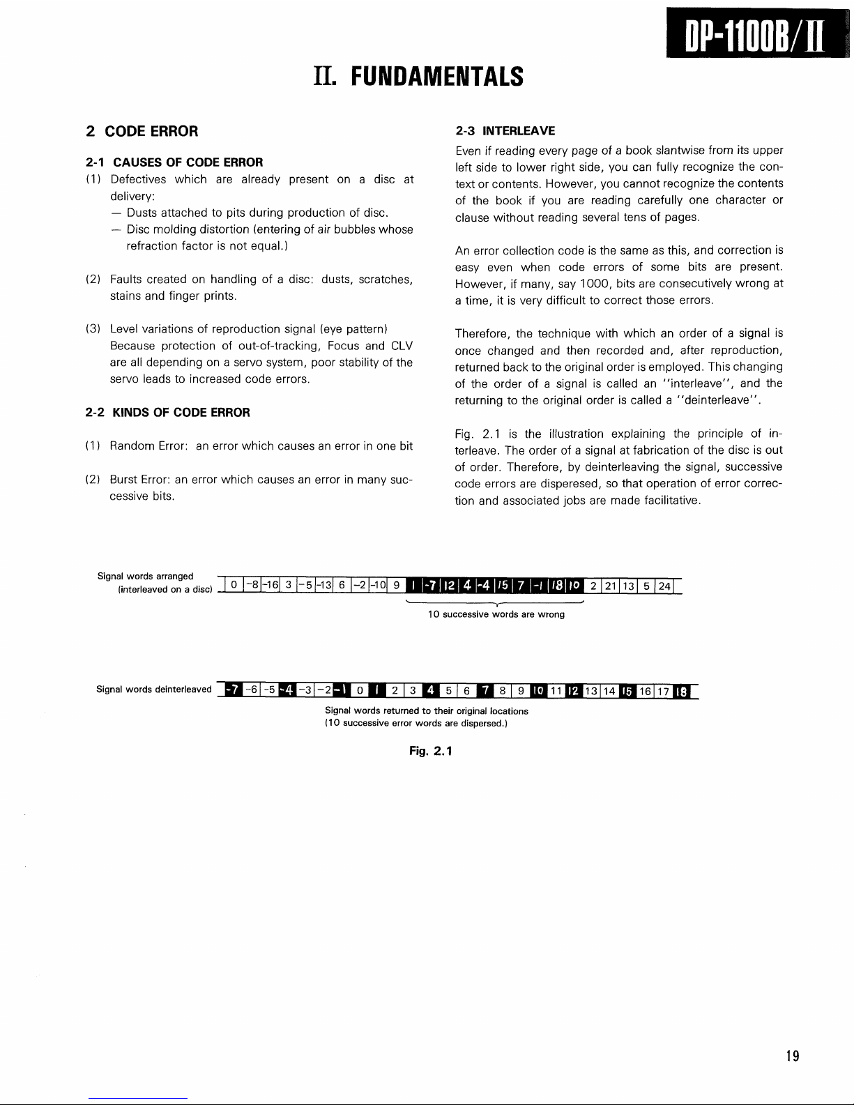
Fig.
2.1 is the illustration explaining the principle of in-
terleave. The order of a signal at fabrication of the disc is out
of order. Therefore, by deinterleaving the signal, successive
code errors are disperesed, so that operation of error correc-
tion and associated jobs are made facilitative.
Signal
words arranged
(interleaved on a
disc)
10
successive
words are wrong
Signal
words returned to their original locations
(10
successive
error words are
dispersed.)
Fig.
2.1
1
Signal
words deinterleaved
•P-1100B
2-4
SINGLE
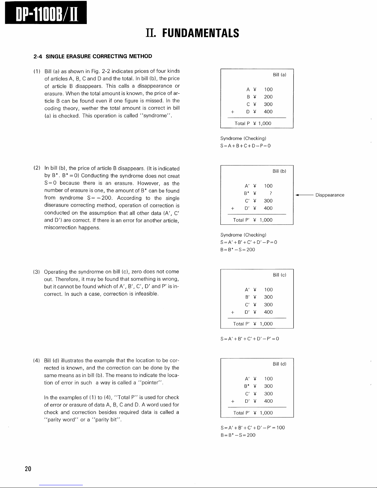
Bill
(a) as
of articles
of article B disappears. This calls a disappearance
erasure. When
ticle
B can be
coding theory, wether
(a)
is
checked. This operation
(2) In
bill (b),
by
B*. B*=0)
S
= 0
because there
number
of
from syndrome
diserasure correcting method, operation
conducted
and
D') are
miscorrection happens.
II
ERASURE
shown
in
A, B, C
the
found even
the
price
Conducting
erasure
S=-200.
on the
correct.
CORRECTING
Fig.
2-2
indicates prices
and D and
total amount
of
is
assumption that
If
the
is
if one
the
total amount
is
article B disappears.
the
syndrome does
is an
erasure. However,
one,
the
amount
According
there
is an
II.
FUNDAMENTALS
METHOD
of
four kinds
total.
In
bill (b),
the
price
known,
the
price
of ar-
figure
is
missed.
is
called "syndrome".
(It is
of B* can be
to the
of
all
other data
error
for
another article,
In the
correct
in
indicated
not
as the
single
correction
(A', C
creat
found
or
bill
is
A ¥ 100
B
200
¥
C ¥ 300
+
D
Total
Syndrome (Checking)
S=A+B+C+D-P=0
+
D'
Total
Syndrome (Checking)
S = A' + B' + C' + D'-P = 0
B = B*-S = 200
¥ 400
¥
1,000
P
A' ¥ 100
B*
¥
¥ 300
C
400
¥
P'
¥ 1,000
Bill
?
Bill
(a)
(b)
Disppearance
(3)
Operating
out. Therefore,
but
it
correct.
(4)
Bill
(d)
rected
same means
tion
of
In
the
of error
check
"parity word"
the
syndrorme
it may be
cannot
be
found which
In
such a case, correction
illustrates
is
error
examples
or
and
the
known,
and the
as in
in
such
of (1) to
erasure
correction besides required data
or a
on
bill
found that something
of
example that
correction
bill (b).
The
a way is
(4), "Total
of
data
A, B, C
"parity
bit".
means
called a "pointer".
(c),
zero does
A',
B', C, D' and P' is in-
is
infeasible.
the
location
can be
to
P" is
and
D. A
done
indicate
used
word used
is
not
is
to be
the
for
called
come
wrong,
cor-
by the
loca-
check
for
a
Bill
(c)
¥ 100
A'
300
¥
B'
300
¥
C
400
+
D'
Total
S = A' + B' + C' + D'-P' = 0
+
D'
Total
S = A' + B' + C' + D'-P' = 100
B = B*-S = 200
¥
P'
¥ 1,000
A' ¥
B* ¥ 300
C ¥
P'
100
300
¥ 400
¥ 1,000
Bill
(d)
20
II.
FUNDAMENTALS
2-5
SINGLE ERROR CORRECTION, DOUBLE ERASURES
In case of (3) in 2-4, correction is infeasible because the
location of error is unknown. Even in such a case, the
way by which correction is feasible is a single error cor-
recting method. In 2-4, there is only one parity
word,
P.
Besides this, a "Weighted Total Value", Q, is
used.
Because two parity words P and Q are
used,
there are
also two syndromes Sj And S2.
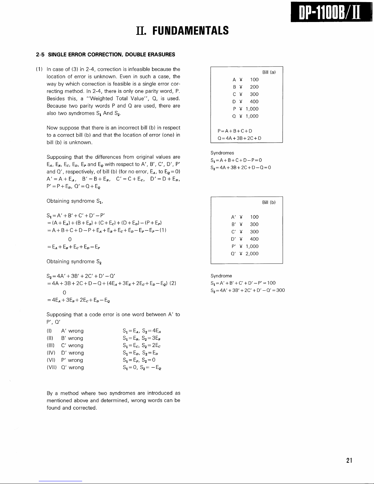
Now suppose that there is an incorrect bill (b) in respect
to a correct bill (b) and that the location of error (one) in
bill (b) is unknown.
Supposing that the differences from original values are
EA,
EB, Ec, EDl EP and Ee with respect to A', B', C, D', P'
and Q', respectively, of bill (b) (for no error, EA, to EQ = 0)
k' = k + EAl B' = B + EB, C' = C + EC, D' = D + ED,
P' = P + EDl Q' = Q + E
Q
Obtaining syndrome S
v
51 = A' + B' + C' + D'-P'
= (A+EJ + (B + EB) + (C + EC) + (D +
ED)-(P
+ EP)
= A+B + C+D-P + Eyl +
EB+Ec+E0-EF-Ei,-(1)
0
=
EA +
EB+EC+ED-E
P
Obtaining syndrome S
2
52 = 4A' + 3B' + 2C' + D'-Q'
= 4A + 3B + 2C + D-Q + (4E^ + 3E£+2EC+ED-EQ) (2)
0
=
4E4
+ 3EB+2EC+ED-E
Q
Supposing that a code error is one word between A' to
P', Q'
(I)
A'wrong Sj = E^, S2 = 4E
A
(II)
B'wrong S1 = Efl, S2 = 3E
B
(III)
C wrong S1 = EC, S2 = 2E
C
(IV)
D'wrong S^E^, S2=E
D
(VI)
P'wrong S^Ep, S2 = 0
(VII)
Q'wrong St = 0, S2=-E
e
By a method where two syndromes are introduced as
mentioned above and determined, wrong words can be
found and corrected.
Bill (a)
A ¥
100
B ¥
200
C ¥
300
D ¥
400
P ¥
1,000
Q ¥
1,000
P=A+B+C+D
Q = 4A + 3B + 2C + D
Syndromes
S
1 =
A + B + C + D-P = 0
S, = 4A + 3B + 2C + D-Q = 0
Bill (b)
A' ¥ 100
B' ¥ 300
C ¥ 300
D'
¥
400
?' ¥
1,000
Q' ¥ 2,000
Syndrome
S^A' + B' + C' + D'-P'^OO
S, = 4A' +
3B' + 2C'
+ D'-Q' = 300
DP-1100B
II
II.
FUNDAMENTALS
(2)
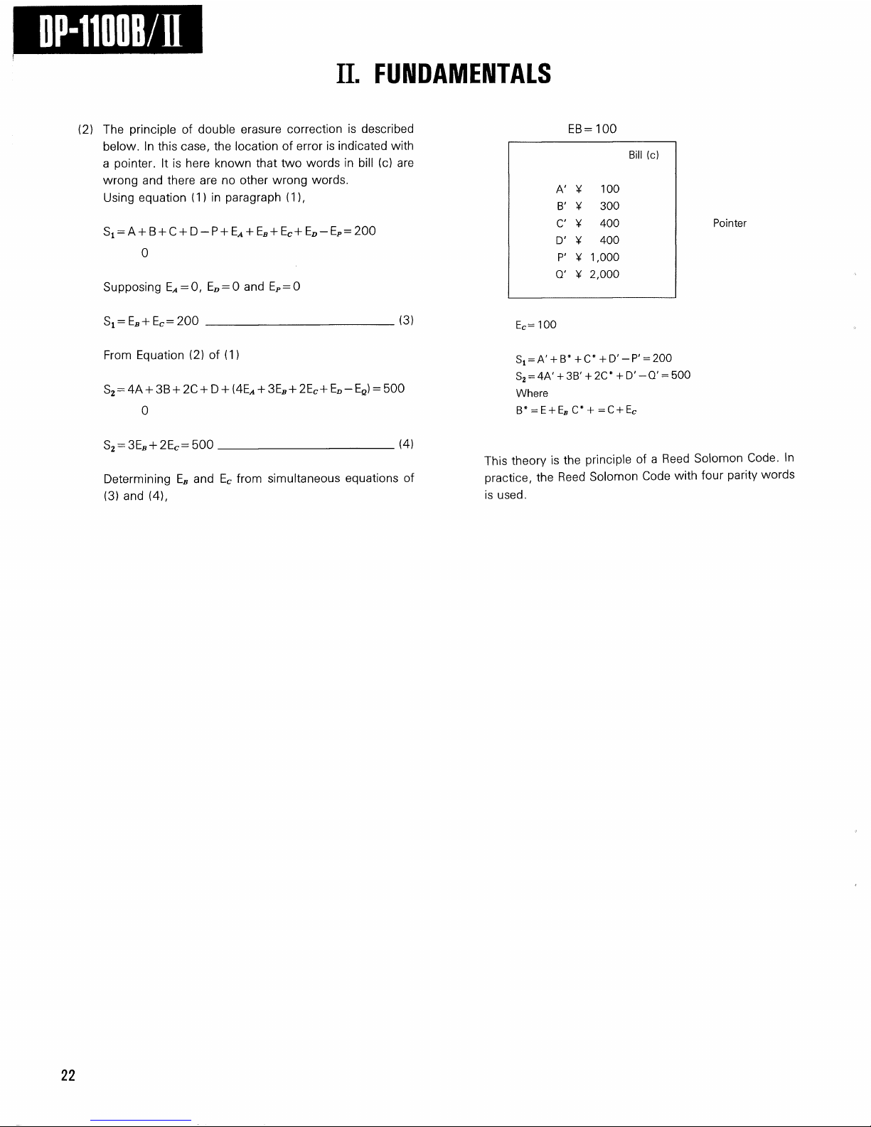
The principle of double erasure correction is described
below. In this case, the location of error is indicated with
a pointer. It is here known that two words in bill (c) are
wrong and there are no other wrong words.
Using equation (1) in paragraph (1),
S1 = A + B + C + D-P + Eyl + Efl+Ec+ED-EP=200
0
EB=100
Supposing EA = 0, ED = 0 and EP = 0
S1 = EJ,+ EC=200
(3)
From Equation (2) of (1
S2 = 4A + 3B + 2C + D + (4E/4 + 3EB + 2Ec+EB-EQ) = 500
0
Bill (c)
A' ¥
100
B' ¥
300
C ¥
400
D'
¥
400
P' ¥
1,000
Q' ¥
2,000
Pointer
Ec=100
51 = A' + B*+C* + D'-P' = 200
52 = 4A' + 3B' + 2C* + D' — Q' = 500
Where
B* = E + EBC* + =C + E
C
S2 = 3EJJ+2EC=500
(4)
Determining EB and Ec from simultaneous equations of
(3)
and (4),
This theory is the principle of a Reed Solomon Code. In
practice, the Reed Solomon Code with four parity words
is used.
22
DP-1100B II
II.
FUNDAMENTALS
2-6
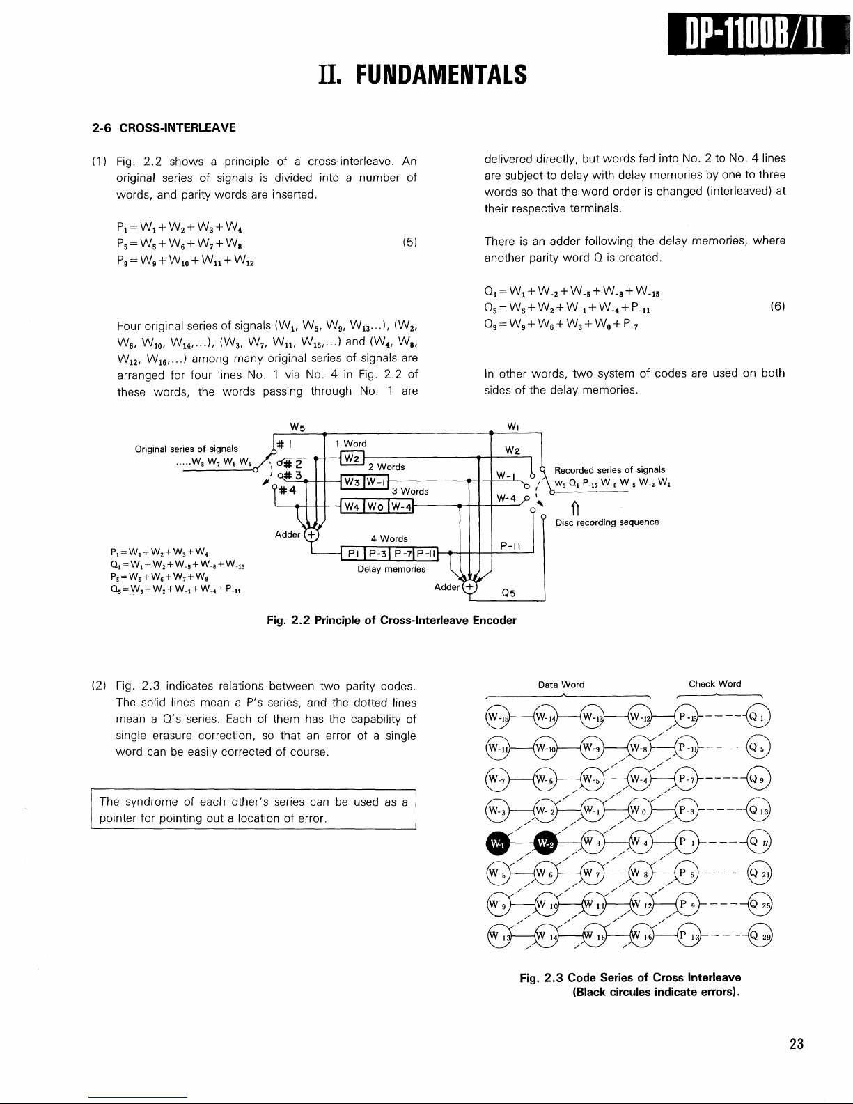
CROSS-INTERLEAVE
Fig.
2.2 shows a principle of a cross-interleave. An
original series of signals is divided into a number of
words, and parity words are inserted.
P1 =
W1 +
W2 +
W3 +
W
4
P5 =
W5 +
W6 +
W7 +
W
8
P9 =
W9 +
W10 + WN + W
12
(5)
delivered directly, but words fed into No. 2 to No. 4 lines
are subject to delay with delay memories by one to three
words so that the word order is changed (interleaved) at
their respective terminals.
There is an adder following the delay memories, where
another parity word Q is created.
Four original series of signals (W1( W5, W9,
W13...),
(W2,
W6, W10,
Wu,...),
(W3, W7, Wu, W15,...) and (W4, W8,
W12, W16,...) among many original series of signals are
arranged for four lines No. 1 via No. 4 in Fig. 2.2 of
these words, the words passing through No. 1 are
Q1 =
W1 +
W.2 + W.5 +
W-8 +
W.
15
Q5 = W5 + W2 + W.1 + W.4+P.U (6)
Q9 =
W9 +
W6 +
W3 +
W0 +
P.?
In other words, two system of codes are used on both
sides of the delay memories.
Original
series
of signals
,W8 W7 W6 W
5
p1=w1+w2+w3+w
4
Qt =
Wj + W2 +
W_5 +
W_„ + W.
15
PS =
W5 +
W6 +
W7 +
W
8
Q5 =
W5 +
W2 +
W.n + W_4 +
P_
n
Recorded
series
of signals
w5 Qt P.15 W_8 W.5 W.2 W
t
Disc
recording sequence
Fig.
2.2 Principle of
Cross-Interleave
Encoder
(2)
Fig. 2.3 indicates relations between two parity codes.
The solid lines mean a P's series, and the dotted lines
mean a Q's series. Each of them has the capability of
single erasure correction, so that an error of a single
word can be easily corrected of course.
The syndrome of each other's series can be used as a
pointer for pointing out a location of error.
Fig.
2.3
Code
Series
of
Cross
Interleave
(Black
circules
indicate
errors).
1
Word
2
Words
3
Words
4
Words
Adder
Delay
memories
Adder
Data
Word
Check
Word
P-1100B
II
II.
FUNDAMENTALS
3 BRIEF
EXPLANATIONS
ON CD
PLAYER
(See
the
BLOCK
DIAGRAM)
3-1
PICKUP
FOR CD
APPLICATION
A pickup part corresponding to a cartridge for a conventional
analog player is detailed later. Briefly speaking, this part
allows the laser diode to emit a light beam (X=780 nm) and
convert the intensity of the reflected light from disc pits into
electric signals.
3-2
SIGNAL
PROCESSING
CIRCUIT
A signal detected at a pickup is delivered to a signal process-
ing circuit, and split into the following three signals.
(1)
Focus Error Signal
(2)
tracking (Radial) Error Signal
(3)
Radio Frequency (RF) Signal: This signal is processed to
generate an analog signal.
3-3
SERVO
CIRCUIT
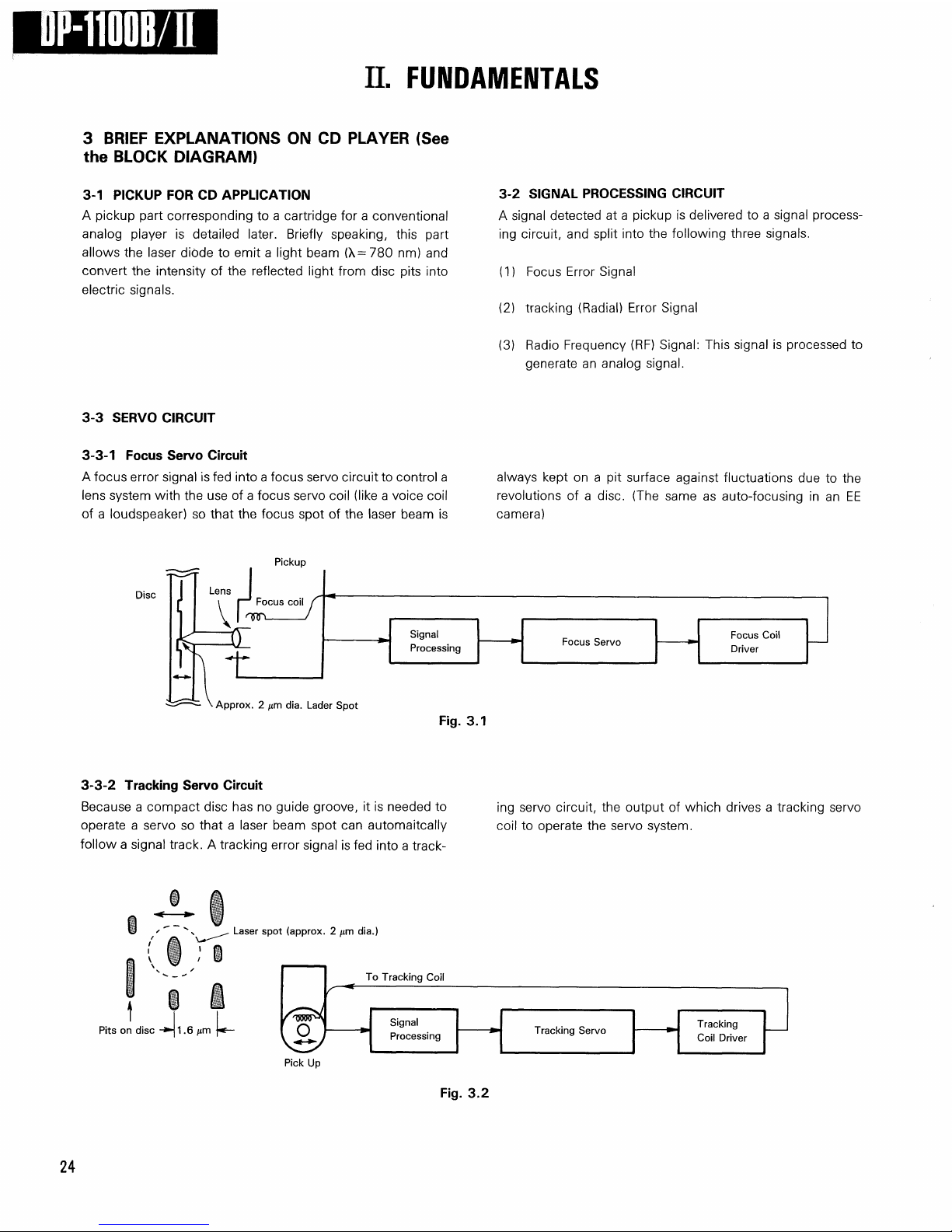
3-3-1
Focus
Servo
Circuit
A focus error signal is fed into a focus servo circuit to control a
lens system with the use of a focus servo coil (like a voice coil
of a loudspeaker) so that the focus spot of the laser beam is
always kept on a pit surface against fluctuations due to the
revolutions of a disc. (The same as auto-focusing in an EE
camera)
Disc
Lens
Signal
Processing
Focus
Servo
Focus
Coil
Driver
•
Approx. 2 nm dia.
Lader
Spot
Fig.
3.1
3-3-2 Tracking
Servo
Circuit
Because a compact disc has no guide groove, it is needed to
operate a servo so that a laser beam spot can automaitcally
follow a signal track. A tracking error signal is fed into a track-
ing servo circuit, the output of which drives a tracking servo
coil to operate the servo system.
Pits
on
disc
Laser
spot (approx. 2 /tm dia.
Tracking
Servo
Tracking
Coil
Driver
Pick
Up
Fig.
3.2
24
Pickup
Focus
coil
1.6 nm
To
Tracking
Coil
Signal
Processing
DP-1100B II
II.
FUNDAMENTALS
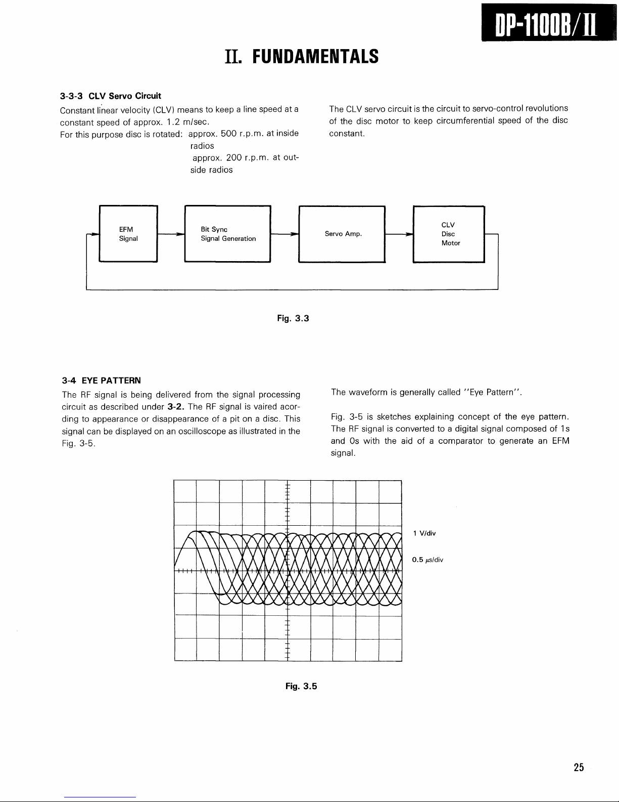
3-3-3 CLV
Servo
Circuit
Constant linear velocity (CLV) means to keep a line speed at a
constant speed of approx. 1.2
m/sec.
For this purpose disc is rotated: approx. 500 r.p.m. at inside
radios
approx. 200 r.p.m. at out-
side radios
The CLV servo circuit is the circuit to servo-control revolutions
of the disc motor to keep circumferential speed of the disc
constant.
Fig.
3.3
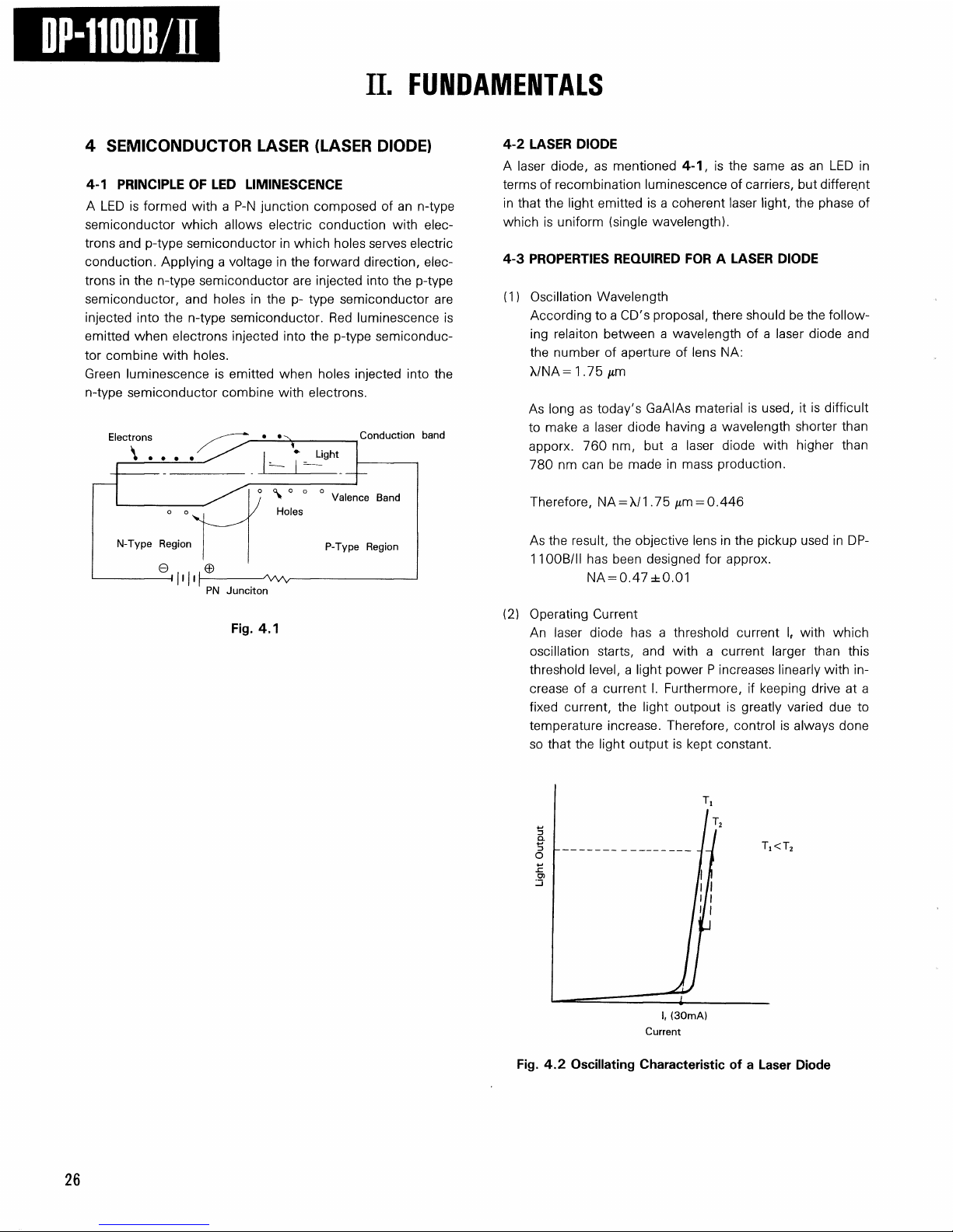
3-4 EYE
PATTERN
The RF signal is being delivered from the signal processing
circuit as described under 3-2. The RF signal is vaired acor-
ding to appearance or disappearance of a pit on a disc. This
signal can be displayed on an oscilloscope as illustrated in the
Fig.
3-5.
The waveform is generally called "Eye Pattern".
Fig.
3-5 is sketches explaining concept of the eye pattern.
The RF signal is converted to a digital signal composed of 1s
and Os with the aid of a comparator to generate an EFM
signal.
Fig.
3.5
25
EFM
Signal
Bit Sync
Signal
Generation
Servo
Amp.
CLV
Disc
Motor
1
V/div
0.5 /ts/div
DP-1100B
II
II.
FUNDAMENTALS
4
SEMICONDUCTOR
LASER
(LASER
DIODE)
4-1
PRINCIPLE
OF LED
LUMINESCENCE
A LED is formed with a P-N junction composed of an
n-type
semiconductor which allows electric conduction with elec-
trons and
p-type
semiconductor in which holes serves electric
conduction. Applying a voltage in the forward direction, elec-
trons in the
n-type
semiconductor are injected into the
p-type
semiconductor, and holes in the p- type semiconductor are
injected into the
n-type
semiconductor. Red luminescence is
emitted when electrons injected into the
p-type
semiconduc-
tor combine with holes.
Green luminescence is emitted when holes injected into the
n-type
semiconductor combine with electrons.
Conduction
band
PN
Junciton
Fig.
4.1
4-2
LASER
DIODE
A laser diode, as mentioned 4-1, is the same as an LED in
terms of recombination luminescence of carriers, but different
in that the light emitted is a coherent laser light, the phase of
which is uniform (single wavelength).
4-3
PROPERTIES
REQUIRED
FOR A
LASER
DIODE
(1)
Oscillation Wavelength
According to a CD's proposal, there should be the follow-
ing relaiton between a wavelength of a laser diode and
the number of aperture of lens NA:
X/NA=1.75 jim
As long as today's GaAIAs material is used, it is difficult
to make a laser diode having a wavelength shorter than
apporx. 760 nm, but a laser diode with higher than
780 nm can be made in mass production.
Therefore, NA = X/1.75 /*m = 0.446
As the result, the objective lens in the pickup used in DP-
1100B/II has been designed for approx.
NA = 0.47±0.01
(2)
Operating Current
An laser diode has a threshold current I, with which
oscillation starts, and with a current larger than this
threshold level, a light power P increases linearly with in-
crease of a current I. Furthermore, if keeping drive at a
fixed current, the light outpout is greatly varied due to
temperature increase. Therefore, control is always done
so that the light output is kept constant.
T,<T
2
Fig.
4.2 Oscillating
Characteristic
of a
Laser
Diode
26
Electrons
N-Type
Region
Holes
Valence
Band
P-Type
Region
Light
Light
Output
I, (30mA)
Current
•P-1100B
II
II.
FUNDAMENTALS
5
PICK-UP
(PU) AND PU
SERVO
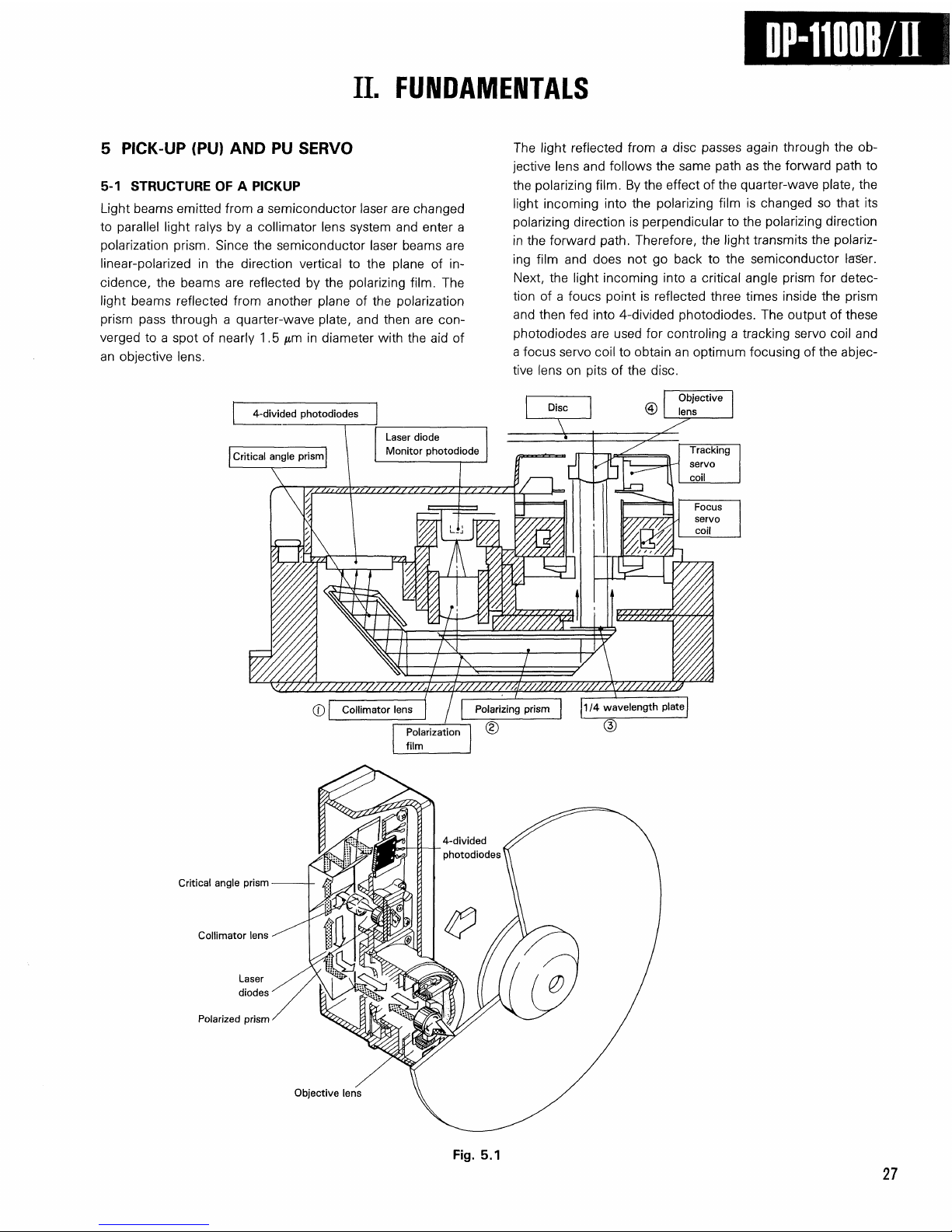
5-1
STRUCTURE
OF A
PICKUP
Light beams emitted from a semiconductor laser are changed
to parallel light ralys by a collimator lens system and enter a
polarization prism. Since the semiconductor laser beams are
linear-polarized in the direction vertical to the plane of in-
cidence, the beams are reflected by the polarizing
film.
The
light beams reflected from another plane of the polarization
prism pass through a quarter-wave plate, and then are
con-
verged to a spot of nearly 1.5 /im in diameter with the aid of
an objective lens.
The light reflected from a disc passes again through the ob-
jective lens and follows the same path as the forward path to
the polarizing
film.
By the effect of the quarter-wave plate, the
light incoming into the polarizing film is changed so that its
polarizing direction is perpendicular to the polarizing direction
in the forward path. Therefore, the light transmits the polariz-
ing film and does not go back to the semiconductor raSer.
Next, the light incoming into a critical angle prism for detec-
tion of a foucs point is reflected three times inside the prism
and then fed into 4-divided photodiodes. The output of these
photodiodes are used for controling a tracking servo coil and
a focus servo coil to obtain an optimum focusing of the abjec-
tive lens on pits of the disc.
4-divided photodiodes
Critical
angle prism
Critical
angle prism
Collimator
lens
Polarized
prism
Objective
lens
Fig.
5.1
27
Laser
diode
Monitor
photodiode
Disc
Objective
lens
Tracking
servo
coil
Focus
servo
coil
Collimator
lens
Polarizing prism
1/4 wavelength plate
Polarization
film
4-divided
photodiodes'
Laser
diodes
DP-1100B
II
II.
FUNDAMENTALS
(1)
Collimator Lens
Diffused light beams are changed to parallel light beams.
Light beams distributed in oval pattern is changed to ap-
prox. circular distributions.
(2)
Polarized Prism
Light polarized in parallel to a surface is reflected, and
light polarized in vertical is passed through the prism.
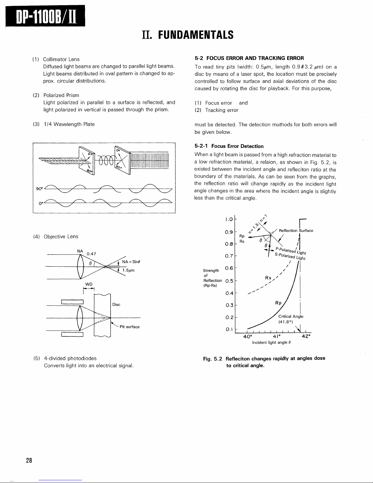
5-2
FOCUS
ERROR
AND
TRACKING
ERROR
To read tiny pits (width: 0.5/im, length 0.9#3.2/*m) on a
disc by means of a laser spot, the location must be precisely
controlled to follow surface and axial deviations of the disc
caused by rotating the disc for playback. For this purpose,
(1)
Focus error and
(2)
Tracking error
must be detected. The detection muthods for both errors will
be given below.
5-2-1
Focus
Error
Detection
When a light beam is passed from a high refraction material to
a low refraction material, a relaion, as shown in Fig. 5.2, is
existed between the incident angle and refleciton ratio at the
boundary of the materials. As can be seen from the graphs,
the reflection ratio will change rapidly as the incident light
angle changes in the area where the incident angle is slightly
less than the critical angle.
(3)
114 Wavelength Plate
NA = Sin0
Pit
surface
(5)
4-divided photodiodes
Converts light into an electrical signal
Fig.
5.2 Refleciton
changes
rapidly at
angles
dose
to critical angle.
28
(4)
Objective Lens
Reflection
Surface
SPola
""1L,
ght
Critical
Angle
(41.8°)
Incident
light
angle
0
Strength
of
Reflection
(Rp-Rs)
1.5/xm
Disc
WD
NA
0.47
II.
FUNDAMENTALS
QP-1100B II
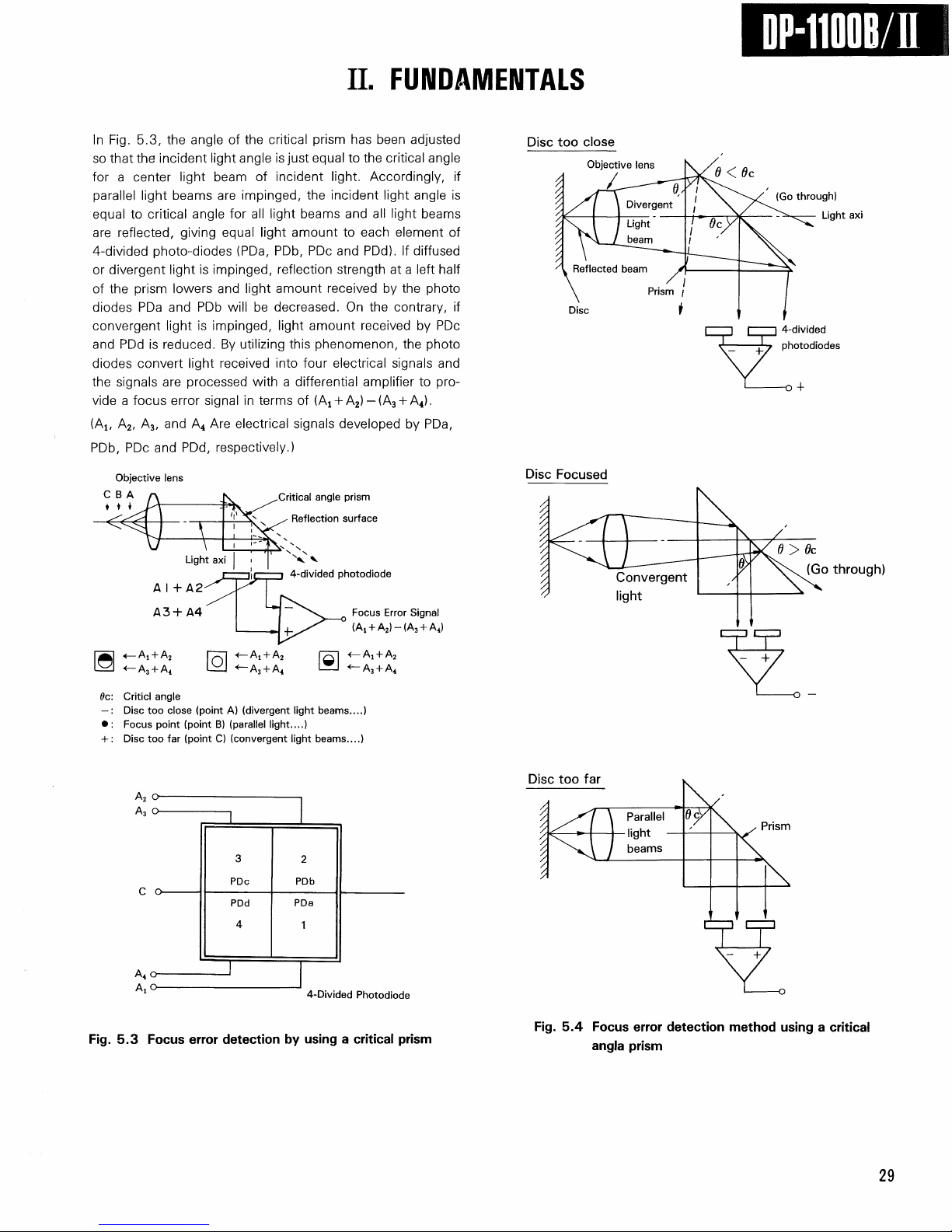
In Fig. 5.3, the angle of the critical prism has been adjusted
so that the incident light angle is just equal to the critical angle
for a center light beam of incident light. Accordingly, if
parallel light beams are impinged, the incident light angle is
equal to critical angle for all light beams and all light beams
are reflected, giving equal light amount to each element of
4-divided photo-diodes (PDa, PDb, PDc and PDd). If diffused
or divergent light is impinged, reflection strength at a left half
of the prism lowers and light amount received by the photo
diodes PDa and PDb will be decreased. On the contrary, if
convergent light is impinged, light amount received by PDc
and PDd is reduced. By utilizing this phenomenon, the photo
diodes convert light received into four electrical signals and
the signals are processed with a differential amplifier to pro-
vide a focus error signal in terms of (At + A2) — (A3 + A4).
(A1( A2, A3, and A4 Are electrical signals developed by PDa,
PDb,
PDc and PDd, respectively.)
^Critical
angle
prism
Reflection
surface
Disc
too
close
4-divided
photodiode
A3 +
A
4
-Ai
+
A
2
A3 +
A
4
Criticl
angle
Disc
too
close
(point A) (divergent light
beams....)
Focus
point (point B)
(parallel
light....)
Disc
too far (point C)
(convergent
light
beams....)
Disc
Focused
Disc
too far
Prism
4-Divided
Photodiode
Fig.
5.3
Focus
error detection by
using
a critical prism
Fig.
5.4
Focus
error detection method
using
a critical
angla
prism
29
Objective
lens
Divergent
Light
beam
Reflected
beam
Disc
Prism
4-divided
photodiodes
(Go
through)
Light
axi
Objective
lens
Light
axi
Focus
Error
Signal
(A!
+ A2)-(A3 + A4)
At +
A
2
A3 +
A
4
Convergent
light
(Go
through)
3
PDc
2
PDb
PDd
4
PDa
1
Parallel
-light
-
beams
DP-1100B II
II.
FUNDAMENTALS
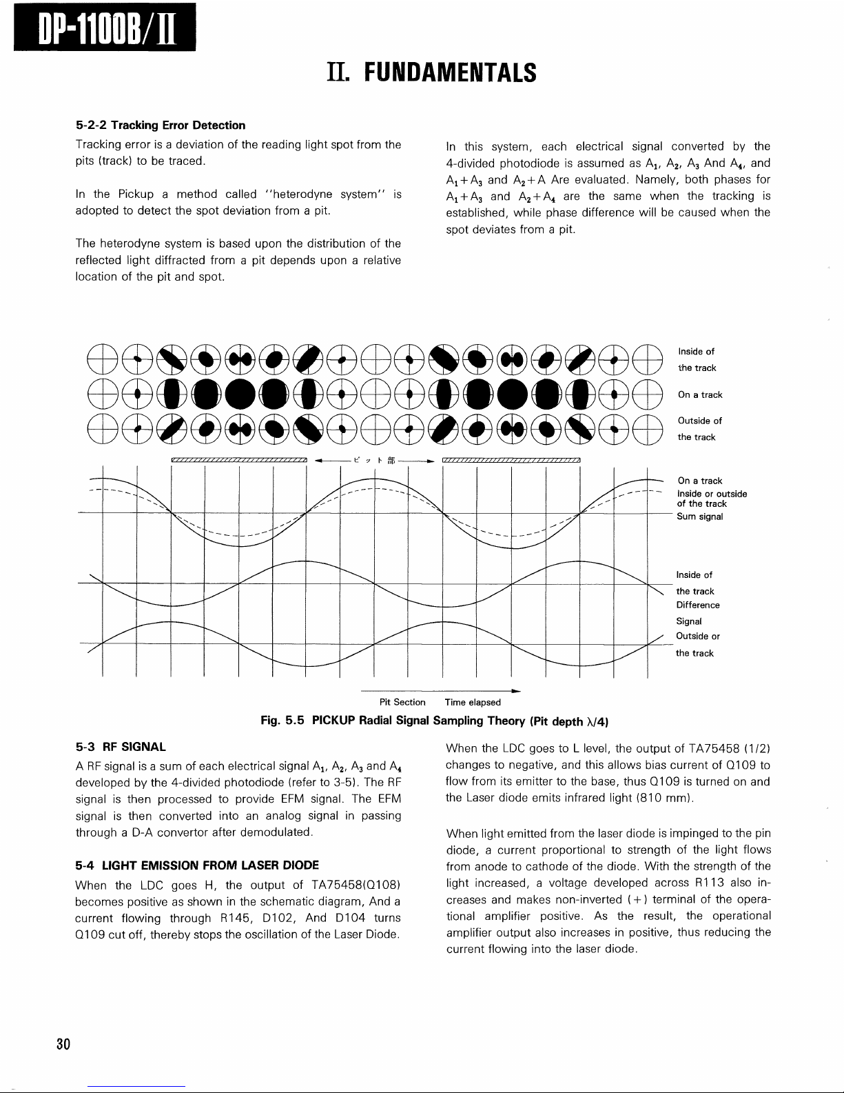
5-2-2 Tracking
Error
Detection
Tracking error is a deviation of the reading light spot from the
pits (track) to be traced.
In the Pickup a method called "heterodyne system" is
adopted to detect the spot deviation from a pit.
The heterodyne system is based upon the distribution of the
reflected light diffracted from a pit depends upon a relative
location of the pit and spot.
In this system, each electrical signal converted by the
4-divided photodiode is assumed as Ax, A2, A3 And A4, and
At + A3 and A2 + A Are evaluated. Namely, both phases for
At + A3 and A2 + A4 are the same when the tracking is
established, while phase difference will be caused when the
spot deviates from a pit.
Fig.
5.5
PICKUP
Radial
Signal
Sampling Theory (Pit depth X/4)
5-3 RF
SIGNAL
A RF signal is a sum of each electrical signal Ax, A2, A3 and A
4
developed by the 4-divided photodiode (refer to 3-5). The RF
signal is then processed to provide EFM signal. The EFM
signal is then converted into an analog signal in passing
through a D-A convertor after demodulated.
5-4 LIGHT EMISSION FROM
LASER
DIODE
When the LDC goes H, the output of TA75458(Q108)
becomes positive as shown in the schematic diagram, And a
current flowing through R145, D102, And D104 turns
Q109 cut off, thereby stops the oscillation of the Laser Diode.
When the LDC goes to L level, the output of TA75458 (1/2)
changes to negative, and this allows bias current of Q109 to
flow from its emitter to the base, thus Q109 is turned on and
the Laser diode emits infrared light (810 mm).
When light emitted from the laser diode is impinged to the pin
diode,
a current proportional to strength of the light flows
from anode to cathode of the diode. With the strength of the
light increased, a voltage developed across R113 also in-
creases and makes non-inverted (+) terminal of the opera-
tional amplifier positive. As the result, the operational
amplifier output also increases in positive, thus reducing the
current flowing into the laser diode.
30
Inside
of
the track
On a track
Outside
of
the track
On a track
Inside
or outside
of the track
Sum
signal
Inside
of
the track
Difference
Signal
Outside
or
the track
Pit
Section
Time
elapsed

DP-1100B
II
II.
FUNDAMENTALS
6.
GENERAL
DESCRIPTION
ON
MICROPROCESSOR
6-1 Address Data (Q Signal)
1)
Address Data (Q Signal) Reading Section
In the CD system specifications, one symbol consisting
of 8 bits and located after frame synchronization signal of
PCM data is called CONTROL & DISPLAY SYMBOL, and
each of 8 bits is called P-Channel, Q-Channel,
R-Channel....& W-Channel. Of the eight channels,
Q-Channel is used for address data and one address data
is comprized of 98 frame Q-Channel data. Fig. 5.6
shows this configuration of the CONTROL & DISPLAY
symbol data.
Fig.
6-1
Frame
Syn-
chroniza-
tion
Signal
Frame
Syn-
chroniza-
tion
Signal
Frame
Syn-
chroniza-
tion
Signal
Frame
Syn-
chroniza-
tion
Signal
Frame
Syn-
chroniza-
tion
Signal
User's
bit
After
conversion of 8 bits to 14 bits
CONTROL
DISPLAY
Symbol
DP-1100B
II
II.
FUNDAMENTALS
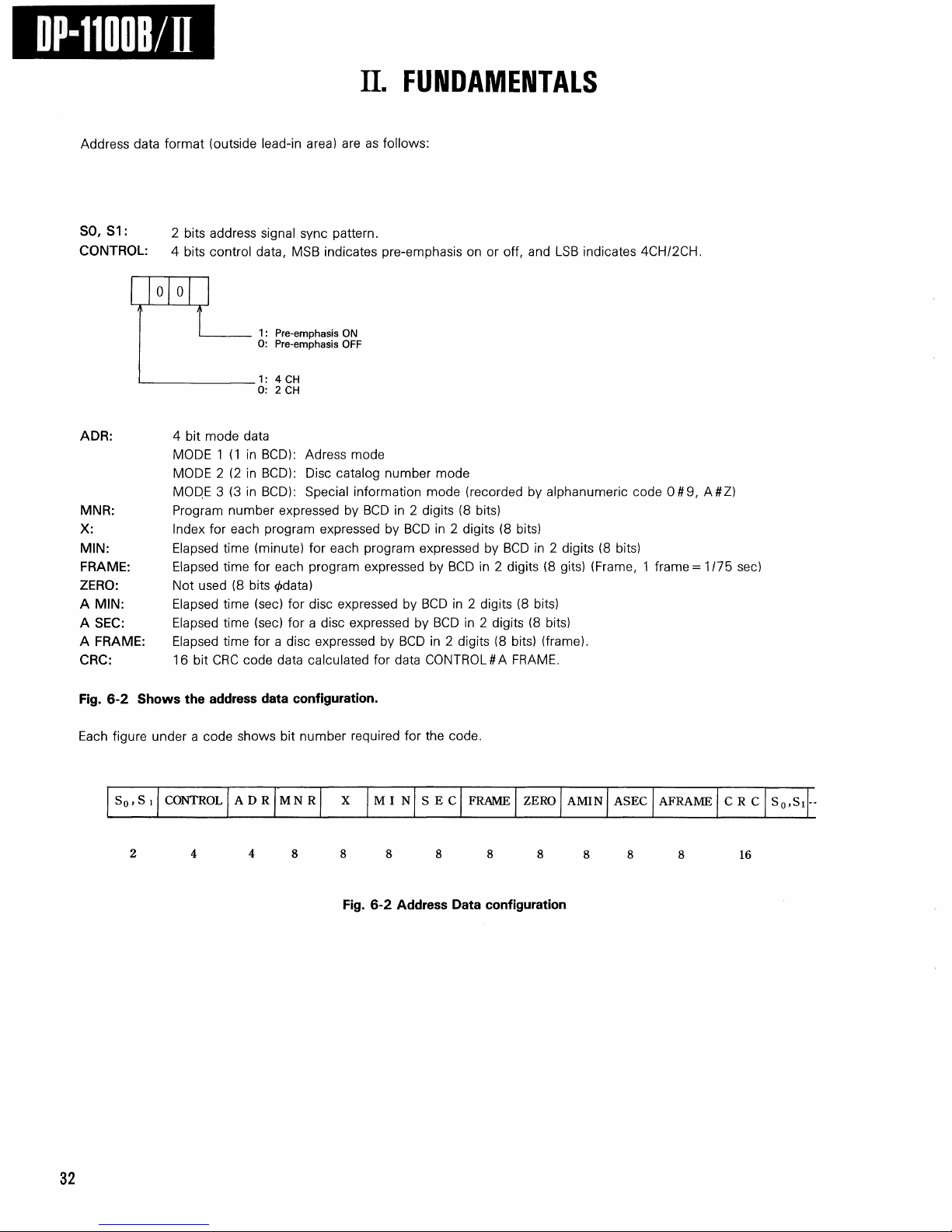
Address data format (outside lead-in area) are as follows:
SO,
S1: 2 bits address signal sync pattern.
CONTROL:
4 bits control data, MSB indicates pre-emphasis on or off, and LSB indicates 4CH/2CH.
1: Pre-emphasis ON
0: Pre-emphasis OFF
1:
4 CH
0: 2 CH
ADR:
4 bit mode data
MODE 1 (1 in BCD): Adress mode
MODE 2 (2 in BCD): Disc catalog number mode
MODE 3 (3 in BCD): Special information mode (recorded by alphanumeric code 0#9, A#Z)
MNR: Program number expressed by BCD in 2 digits (8 bits)
X:
Index for each program expressed by BCD in 2 digits (8 bits)
MIN: Elapsed time (minute) for each program expressed by BCD in 2 digits (8 bits)
FRAME:
Elapsed time for each program expressed by BCD in 2 digits (8 gits) (Frame, 1 frame = 1/75 sec)
ZERO:
Not used (8 bits <£data)
A
MIN: Elapsed time (sec) for disc expressed by BCD in 2 digits (8 bits)
A
SEC:
Elapsed time (sec) for a disc expressed by BCD in 2 digits (8 bits)
A
FRAME:
Elapsed time for a disc expressed by BCD in 2 digits (8 bits) (frame).
CRC:
16 bit CRC code data calculated for data CONTROL#A FRAME.
Fig.
6-2
Shows
the
address
data configuration.
Each figure under a code shows bit number required for the code.
s
0
>
S i
CONTROL
ADR
MN R
X
M I N
SEC
FRAME
ZERO
AMIN
ASEC
AFRAME
CRC
SQISI
2
4
4
8
8
8 8 8
8
8 8
8
16
Fig.
6-2
Address
Data configuration
32
DP-1100B
II
1.
CIRCUIT
DESCRIPTION
Subsequent to "1-2 Head amp", the servo PCB and the
process PCB are described in order along the RF signal flow.
1-1 Head amplifier
The four signals from the pickup are input to preamplifier IC
(Q103) on the mechanism PCB.
1- 1-1
Focus
balance and SVC operation circuit
(Q103)
The internal block diagram of Q103 is shown in section
2-
1-1.
Through the resistors, connected between pins 1 and
2 and between pins 15 and 16 of Q103 (TA7731P), focus
balance and SVC operation (described later) are performed.
Weak signal is amplified and output to servo PCB as S1 and
S2.
1-1-2
Focus
error
signal
generation circuit (Q101 and Q104)
The FE amplifier and peak detector, consisting of Q101 and
Q104,
is a circuit to generate the focus error signal. Peak
detection is made with the B-E diode characteristic of Q104
and the CR time constant of its emitter. The focus error signal
is obtained from (C + D) - (A + B) operation of the picked-up
four signals from the pickup by Q101.
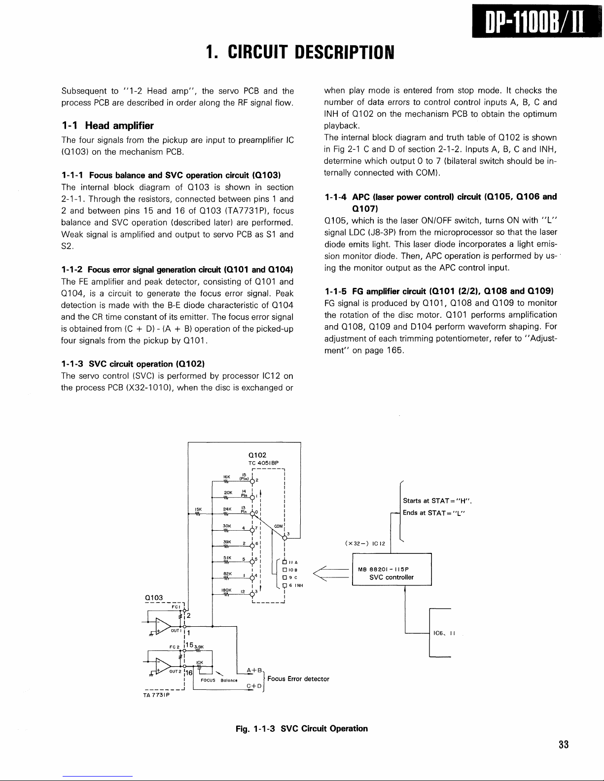
1-1-3 SVC circuit operation
(Q102)
The servo control (SVC) is performed by processor IC12 on
the process PCB (X32-1010), when the disc is exchanged or
when play mode is entered from stop mode. It checks the
number of data errors to control control inputs A, B, C and
INH of Q102 on the mechanism PCB to obtain the optimum
playback.
The internal block diagram and truth table of Q102 is shown
in Fig 2-1 C and D of section 2-1-2. Inputs A, B, C and INH,
determine which output 0 to 7 (bilateral switch should be in-
ternally connected with COM).
1-1-4 APC
(laser
power control) circuit (Q105, Q106 and
Q107)
Q105,
which is the laser ON/OFF switch, turns ON with "L"
signal LDC (J8-3P) from the microprocessor so that the laser
diode emits light. This laser diode incorporates a light emis-
sion monitor diode. Then, APC operation is performed by us-
ing the monitor output as the APC control input.
1-1-5 FG amplifier circuit (Q101 (2/2), Q108 and Q109)
FG signal is produced by Q101, Q108 and Q109 to monitor
the rotation of the disc motor. Q101 performs amplification
and Q108, Q109 and D104 perform waveform shaping. For
adjustment of each trimming potentiometer, refer to "Adjust-
ment" on page 165.
Fig.
1-1-3 SVC
Circuit
Operation
33
 Loading...