

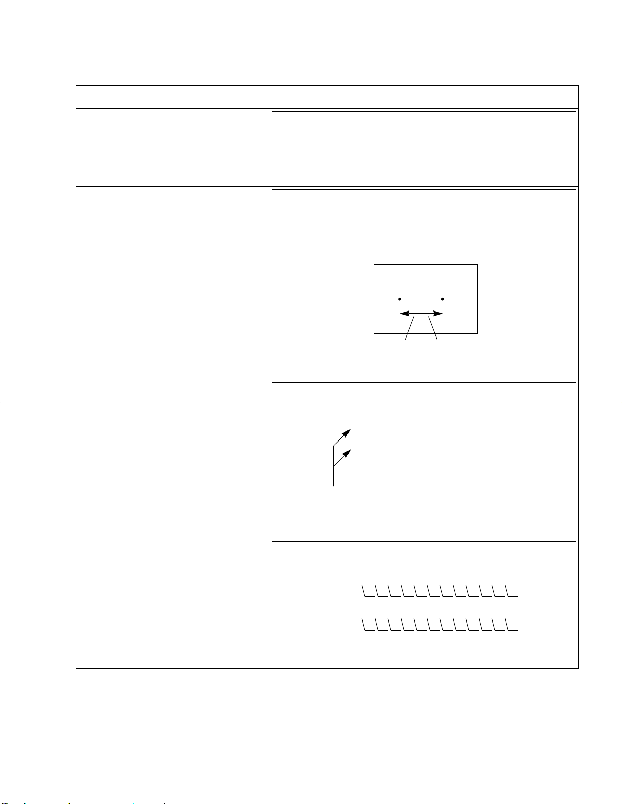
Kenwood CS-5375-HU, CS-5355-HU Service Manual

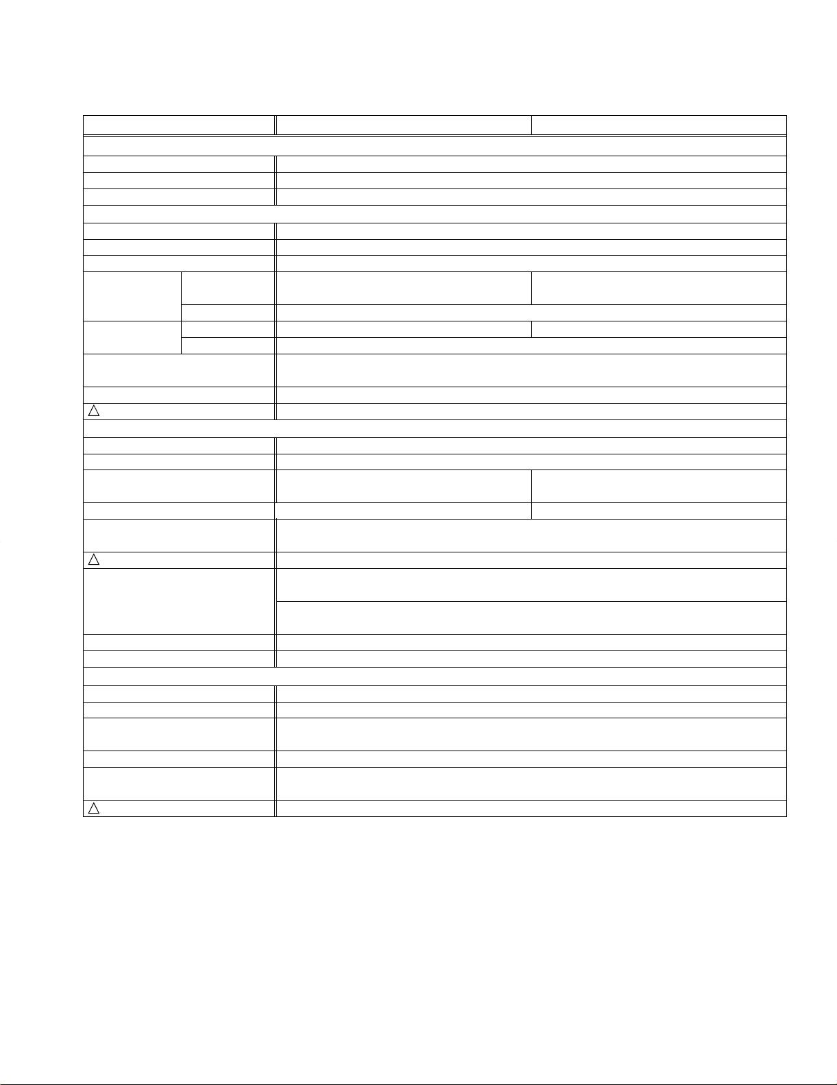
100MHz OSCILLOSCOPE
100MHz
OSCILLOSCOPE
CS–5375
POWER
ON/ OFF
1Vp-p ~ 1KHz
TRACE
ROTA
SCALE ILLUM
FOCUS
INTENSITY CAL
DELAY POSITION
TRIGGERING
HOLDOFF
SLOPE
LEVEL
POSITION
CH 2 INV
MAG
X10
TRACE SEP
NORM
INCR
COARSE FINE
–+
INPUT
400V PK MAX
CAT 1
CH3
POSITION
POSITION
POSITION
23
INPUT
400V PK MAX
CAT 1
INPUT
50V PK MAX
CAT 1
2
3
23
23
0.1V/DIV
~
_
_
_
—
_
—
_
—
_
—
_
—
A
MODE
CH1
CH2
CH3
CHOP
ALT
H.MODE COUPLING
SOURCE
MODE
ALT
AC
HF
FEJ
VERT
MODE
AUTO
DC
CH2
CH3
CH1
NORM
B TRIG`D
AFT.DLY
TV
FRAME
TV
LINE
SINGLE
RESET
REDAY
LINE
B
X-Y
CH 1or Y
CH 2 or X
.1
.2
.5
1
2
5
50
20
10
5
2
1
.1
.2
.5
1
2
5
50
20
10
5
2
1
VOLTS/DIV
VOLTS/DIV
.1.2
.5
1
2
5
10
20
50
.1
.2
.5
.05
.1
.2
.5
1
2
5
10
20
50
CAL
S
VARIABLEVARIABLE
CAL
ADD
mV
mV
AC
DC
AC
DC
GND
GND
A
B
SWEEP TIME / DIV
µs
VARIABLE
ms
CH3
HORIZONTAL
CAL
—
_
SELECTOR
~LINE VOLTAGE
FUSE 250V
100
120
220
230
100V
120V
220V
230V
T 1.0A
T 400mA
100
230
220
120
CAUTION
TO AVOID ELECTRIC SHOCK THE POWER
CORD PROTECTIVE GROUNDING CONDUCTOR
MUST BE CONNECTED TO GROUND.
FOR CONTINUED PROTECTION AGAINST FIRE,
REPLACE ONLY WITH FUSE OF THE SPECIFIED
VOLTAGE AND CURRENT RATINGS.
DISCONNECT POWER SUPPLY BEFORE REPLACING FUSE.
DO NOT REMOVE COVER.
REFER SERVICING TO QUALIFIED PERSONNEL.
Z AXIS INPUT
42V PK MAX
CHI OUTPUT
MAX 5V RMS
KENWOOD T M I CORPORATION MADE IN JAPAN
CS-5355/CS-5375
KENWOOD TMI CORPORATION
SERVICE MANUAL
© 1997-10/B51-1135-00 (K/K)
Model No. plate
Filter
(B11-0518-04)
(CS-5355 ; B73-0191-04)
(CS-5375 ; B73-0189-04)
Knob
(K27-0590-04)
Knob ; lever
(K27-3618-14)
Decorative panel ; large
(A21-2469-03)
Mold panel ; Large
(K63-0110-01)
Push SW
(K24-3005-04)
Handle
(K01-0561-02)
Decorative panel ; small
(A21-2471-04)
Knob
(K29-0877-04)
Rubber foot
(J02-0540-05)
Knob
(K29-0890-03)
AC selector
(E68-0619-05)
Knob
(K29-0891-03)
Rear panel
(A83-0120-02)
Knob
(Large ; K21-0940-04)
(Small ; k21-0955-04)
Cord wrap
(W01-0503-04)

CS-5355/5375
WARNING
The following instructions are for use by qualified personnel only. To avoid electric shock,
do not perform any servicing other than contained in the operating instructions unless you
are qualified to do so.
CONTENTS
SPECIFICATIONS..........................................................................................................3
SAFETY..........................................................................................................................7
ADJUSTMENT................................................................................................................8
PARTS LIST..................................................................................................................16
DISASSEMBLY.............................................................................................................18
PARTS LIST (ELECTRICAL)........................................................................................20
SCHEMATIC DIAGRAM ...............................................................................................48
P.C. BOARD .................................................................................................................85
SEMICONDUCTORS....................................................................................................93
Accessories
LOW CAPACITY PROBE
PC-54(CS-5355)
PC-59(CS-5375)
2
SPECIFICATIONS
Items CS-5375CS-5355
CRT
Type
Acceleration voltage
Effective area
VERTICAL AXIS (Common to channels 1 and 2)
Sensitivity
Attenuation
Input impedance
Frequency
response (-3dB)
(+10 to +35˚C)
Rise time
(+10 to +35˚C)
Signal delay time
Crosstalk
Maximum input voltage
!
5mV to 5V/div
1mV to 2mV/div
5mV to 5V/div
1mV to 2mV/div
The leading edge may be checked using a square wave of the rise time less than that of
this model.
DC : DC to 50MHz
AC : 5Hz to 50MHz
VERTICAL AXIS (CH3)
Sensitivity (+10 to +35˚C)
Input impedance
Frequency response (-3dB)
(+10 to +35˚C)
Rise time (+10 to +35˚C)
Signal delay time
Maximum input voltage
!
Operation
Chop frequency
Channel polarity
The leading edge may be checked using a square wave of the rise time less than that of
this model.
Single trace : CH1, CH2, CH3 or ADD single trace operation
Multi-trace : 2 to 4 traces of CH1, CH2, CH3 and ADD
ALT/CHOP : Display by selecting ALT and CHOP
ADD : Composite waveform of CH1 and CH2 signals are displayed.
HORIZONTAL AXIS (CH2, except for X10 MAG operation)
Sensitivity (+10 to +35˚C)
Input impedance
Frequency response (-3dB)
(+10 to +35˚C)
X-Y phase difference
Operation mode
Maximum input voltage
!
150mm rectangular tube with an integral graticule
8X10 divisions (1 division = 10mm)
1mV, 2mV/div : ±5%, 5mV to 5V/div : ±2%
1-2-5 steps, 12 ranges, fine control between ranges
1MΩ±1%, approx. 20pF
DC : DC to 20MHz, AC : 5Hz to 20MHz
Approx. 7ns
-40dB or less (at 1kHz)
800Vp-p or 400V (DC+AC peak, 1kHz or less)
0.1V/div range : ±2%
1MΩ±1%, approx. 20pF
DC to 50MHz DC to 100MHz
Approx. 7ns Approx. 3.5ns
100Vp-p or 50V (DC+AC peak, 1kHz or less)
Approx. 250kHz (in multi-trace operation)
Normal or inverted, CH2 only inverted
1mV, 2mV/div : ±5%, 5mV to 5V/div : 3%
Same as vertical axis (CH2)
DC : DC to 1MHz, AC : 5Hz to 1MHz
3˚C or less at 100kHz
X-Y mode is selected with H.MODE
CH1 : Y-axis, CH2 : X-axis
Same as vertical axis (CH2)
CS-5355/5375
Approx. 12kV
DC : DC to 100MHz
AC : 5Hz to 100MHz
Approx. 3.5ns
Approx. 17.5ns
3

Items CS-5375CS-5355
SWEEP
Sweep type
Sweep time
(+10 to +35˚C)
Sweep magnified operation
(+10 to +35˚C)
Linearity (+10 to +35˚C)
HOLDOFF
Trace separation
Delayed sweep operation
Delay time
Delay time error (+10 to +35˚C)
Delay jitter
A sweep
B sweep
TRIGGERING
Trigger modes
Trigger signal sources
Trigger coupling
(For trigger sensitivity, see the
table below.)
CS-5355/5375
SPECIFICATIONS
A : A seep
ALT : Alternate A sweep and B sweep
B : B sweep
X-Y : X-Y oscilloscope operation
0.5s to 50ns/div ±3%
1-2-5 steps, 22 ranges,
fine adjustment between ranges
50ms to 50ns/div ±3%
1-2-5 steps, 19 ranges,
fine adjustment between ranges
X10 ±5% (±8% for over 0.5ns/div)
±3% (±5% in X10 MAG operation)
Continuously variable from A sweep NORM position
B sweep is continuously variable by ±4 divisions or more with respect to A sweep.
Continuous delay operation (AFTER DELAY)
Synchronous delay operation (B TRIG'D)
: Synchronous with the trigger signal
Continuous control by 0.2 to 10 divisions for 0.5div to maximum speed sweep
Reading on CRT ±4% + (0 to 300ns)
20000 : 1 of a value 10 times as high as A sweep setting
(A sweep : 1ms/div, B sweep : 1µs/div)
AUTO : Automatic free running with no signal
NORM : Triggered sweep
FIX : Sweep at triggering point set to center of signal amplitude
SINGLE : Single sweep mode
RESET : Restarting single sweep operation
VERT : Input signal selected for V.mode
CH1 : Channel 1 input signal
CH2 : Channel 2 input signal
CH3 : Channel 3 input signal
LINE : Commercial power line
AC : AC coupling from 10Hz
HF
DC : DC coupling
TV-F (TV FRAM)
TV-F (TV LINE)
: Low-pass filter coupling up to 10kHz
REJ
: Composite video signal, vertical synchronization separation.
: Composite video signal, horizontal synchronization separation.
4
Trigger sensitivity (+10 to +35˚C)
CS-5355/5375
SPECIFICATIONS
MODE COUPLING
CS-5355
AC
HF
NORM
AUTO : Same as above specifications for above 40Hz.
(The table shows the sensitivities in terms of the amplitude display on the CRT.)
(>min. for the HF
FIX* : Same as above specifications for above 50Hz.
REJ
DC
TV-F, -L
sensitivity shows that the amplitude necessary for synchronization increases.)
REJ
Items CS-5375CS-5355
10Hz to 20MHz
20M to 50MHz
DC to 20MHz
20M to 50MHz
Signal frequency
10Hz to 50MHz
50M to 100MHz
10Hz to 10kHz
over 10kHz
DC to 50MHz
50M to 100MHz
Composite video signal
CS-5375
NORM
1div
1.5div
1div
>min
1div
1.5div
CALIBRATION SIGNAL : Positive square wave, 1Vp-p ±3%Frequency : Approx. 1kHz
INTENSITY MODULATION
Input voltage
Input impedance
Frequency response
(+10 to +35˚C)
Maximum input voltage
!
84Vp-p or 42V (DC+AC peak, 1kHz or less)
Darkens at TTL level (+5V)
Approx. 10kΩ
DC to 5MHz
CH1 OUTPUT SIGNAL (with 50Ω load)
Output voltage
Output impedance
Frequency
response (-3dB)
1mV/div,
2mV/div
Over 5mV/div
Approx. 50mVp-p/div
Approx. 50Ω
100Hz to 20MHz
100Hz to 100MHz100Hz to 50MHz
TRACE ROTATION : Trace angle is adjustable with a semi-fixed control on panel
POWER SUPPLY
Voltage
Frequency
Power consumption
(Maximum value)
100/120/220/230 VAC (Voltage fluctuation : within±10%)
50Hz or 60Hz
45W, 58VA44W, 57VA
DIMENSIONS AND WEIGHT (Valves enclosed in parentheses include projections.)
Width
Height
Depth
Weight (Approximately)
305mm (344mm)
150mm (165mm)
400mm (459mm)
8.8kg
Sensitivity
(Amplitude)
FIX*
1.5div
2div
1.5div
>min
1.5div
2div
1.5div
5
Items CS-5375CS-5355
ENVIRONMENTAL (Indoor use only)
Altitude
Over voltage Category
Pollution Degree
TEMPERATURE AND HUMIDITY
Operating
Storage
ACCESSORIES
Probe (2 each)
Instruction manual
Adjusting screwdriver
Power cord
Replacement fuse
REGULATORY INFORMATION
LVD
EMI
EMS
CS-5355/5375
SPECIFICATIONS
Up to 2000m
¿
2
0 to 40˚C, 85% RH or less
-20 to 70˚C, 85% RH or less
PC-54 : 10MΩ±2%, 22pF±10%, 1/10 [CS-5355]
1MΩ±2%, 200pF max. (probe only), 1/1
PC-59 : 10MΩ±2%, 12.5pF±10%, 1/10 [CS-5375]
1
1
1
T1Ax1 (for 100V area) or T400mAx1 (for 200V area)
(T : TIME lag fuse)
EN61010-1&A2 (1995)
EN55011 (1991), CLASS B
FCC 47CFR, Part 15, Sub-Part B, Class B
IEC801-2 (1991) 8kVAD
IEC801-3 (1984) 3V/m
IEC801-4 (1988)
7 The specification shown above are subject to change without notice.
6

SAFETY
CS-5355/5375
SAFETY
Before connecting the instrument to a power source, carefully read the following information, then verify that the
proper power cord is used and the proper line fuse is
installed for power source. The specified voltage is shown
on the rear panel. If the power cord is not applied for
specified voltage, there is always a certain amount of danger from electric shock.
Line voltage
This instrument operates using ac-power input voltages
that 100/120/220/230 V at frequencies from 50 Hz to
60Hz.
Power cord
The ground wire of the 3-wire ac power plug places the
chassis and housing of the oscilloscope at earth ground.
Do not attempt to defeat the ground wire connection or
float the oscilloscope ; to do so may pose a great safety
hazard. The appropriate power cord is supplied by an
option that is specified when the instrument is ordered.
The optional power cords are shown as follows in Fig.1
Plug configuration power cord and plug type
North American
120 volt/60 Hz
Rated 15 amp
(12 amp max ; NEC)
Line fuse
The fuse holder is located on the rear panel and contains
the line fuse. Verify that the proper fuse is installed by
replacing the line fuse.
Voltage conversion
This oscilloscope may be operated from either a 100V to
230V, 50/60 Hz power source. Use the following procedure to change from 100 to 230 volt operation or vice
versa.
1. Remove the fuse holder.
2. Replace fuse F1 with a fuse of appropriate value, 1
amp for 100 VAC to 120 VAC operation. 630 m amp for
220 VAC to 230 VAC operation.
3. Reinsert it for appropriate voltage range.
4. When performing the reinsertion of fuse holder for the
voltage conversion, the appropriate power cord should
be used. (See Fig. 1.)
Factory installed
instrument fuse
0.7A, 250V
slow blow
5x20mm
Line cord
plug fuse
None
Parts No. for
power cord
E30-1951-05
Universal Europe
220 volt/50 Hz
Rated 16 amp
U.K.
240 volt/50 Hz
Rated 5 amp
Australian
240 volt/50 Hz
Rated 10 amp
North American
240 volt/60 Hz
Rated 15 amp
(12 amp max ; NEC)
Switzerland
230 volt/50Hz
Rated 10 amp
Fig.1 Power Input Voltage Configuration
0.3A, 250V
slow blow
5x20 mm
0.3A, 250V
slow blow
5x20 mm
0.3A, 250V
slow blow
5x20 mm
0.3A, 250V
slow blow
5x20mm
0.3A, 250V
slow blow
5x20 mm
None
5A
Type C
None
None –
None
E30-1952-05
E30-1963-15
E30-1953-05
–
7

CS-5355/5375
ADJUSTMENT
To obtain the best performance, periodically calibrate the
unit. Sometimes, only one mode need be calibrated, while
at other times, all modes should be calibrated. When one
mode is calibrated, it must be noted that the other modes
may be affected. When calibrating all modes, perform the
calibration in the specified sequence.
The following calibration required an accurate measuring
instrument and an insulated adjusting flat blade screwdriver. If they are not available, contact your dealer. For optimum adjustment, turn the power on and warm up the
scope sufficiently (more than 30 minutes) before starting.
Before calibrating the scope, check the power supply voltage.
TEST EQUIPMENT REQUIRED
The following instrument or their equivalent should be
used for making adjustment.
Test Equipment
Digital Multi Meter
Digital Multi Meter
Square Wave Generator
Sine-Wave Generator (1)
Sine-Wave Generator (2)
Model
DL-712
(KENWOOD TMI)
R-6450
(Advantest)
PG-506
(Tektronix)
SG-503
(Tektronix)
MG3631A
(Anritsu)
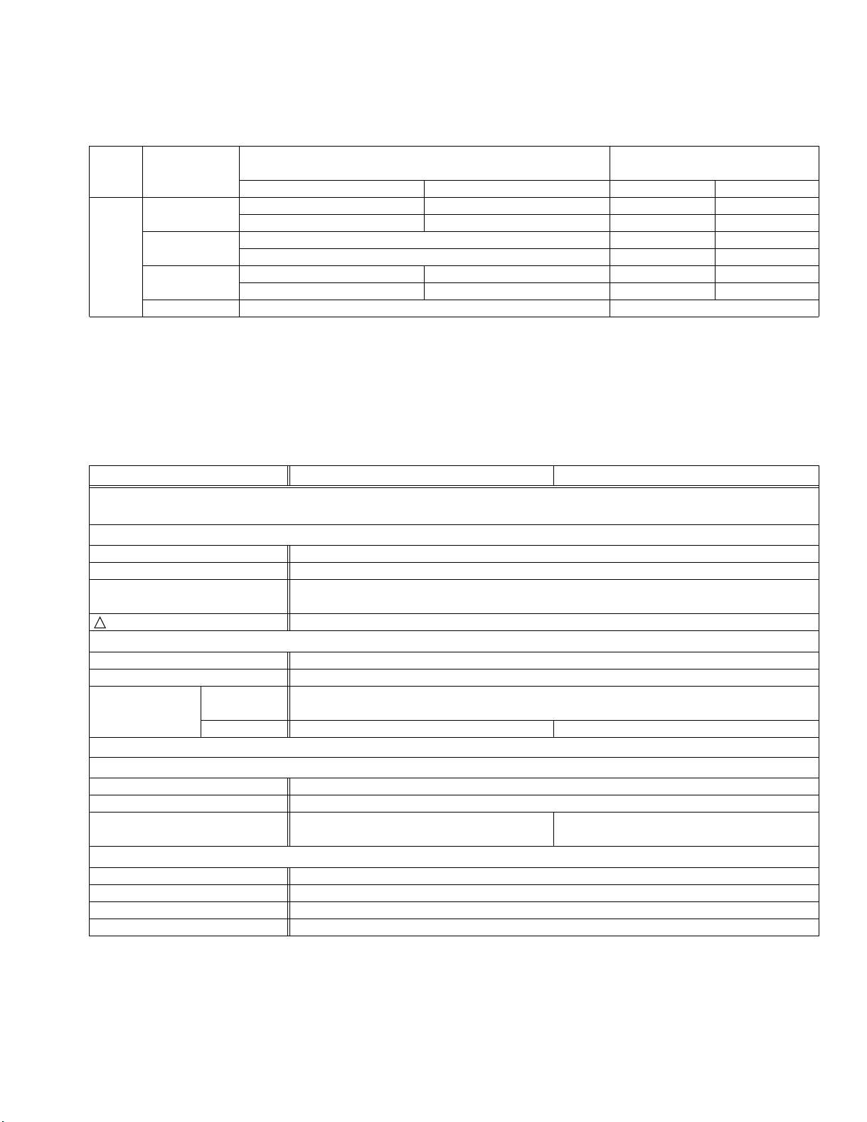
PREPARATION FOR ADJUSTMENT
Control Settings
The control settings listed below must be used for each
adjustment procedure.
Exceptions to these settings will be noted as they occur.
After completing a adjustment, return the controls to the
following settings.
NAME OF KNOBS POSITION
INTENSITY
FOCUS
POSITION
`
` POSITION
VARIABLE
AC-GND-DC
VOLTS/DIV
A/B SWEEP TIME/DIV
COARSE
FINE
HOLDOFF
TRACE SEP
TRIGGERING H.MODE
TRIGGERING COUPLING
TRIGGERING SOURCE
TRIGGERING MODE
TRIGGERING LEVEL
SLOPE
MODE
B TRIG'D/AFT-DLY
X10 MAG
ADD
CH2 INV
12 O'clock
12 O'clock
12 O'clock
12 O'clock
CAL
DC
5V/DIV
Fully counter clock wise
Counter clock wise
Counter clock wise
Fully counter clock wise
Fully counter clock wise
A
AC
VERT MODE
AUTO
12 O'clock
CH1
AFT-DLY
OFF
OFF
OFF
Table 2
Sine-Wave Generator
(Low Frequency)
Time Marker Generator
Oscilloscope
DC standard
Capacitance meter
Color Pattern Generator
Termination –
Table 1
AG-203A
(KENWOOD TMI)
TG-501
(Tektronix)
CS-6040
(KENWOOD TMI)
R6142
(Advantest)
3520
(Hioki)
CG-931
(KENWOOD TMI)
8

CS-5355/5375
ADJUSTMENT
No.
1
2
3
4
Item Adjustment
Operating voltage VR4
Focus center and
ASTIG
Intensity VR101
CH1 Step ATT
Balance
CH1 VARIABLE
Balance
P.C.B.
X73-2210
VR306
VR308
VR102
VR101
VR102 X73-2180
X74-1620
X74-1620
X68-1920
X68-1920
X73-2180
Procedure
V.MODE : CH1, CH2 AC-DC : GND (both CH)
VOLTS : 10mV (both CH) H.MODE : X-Y
R/O : OFF
1) Move the spot to the CRT center by operating the POSI controls.
2) Attach the multimeter probes across CN105-1 on 3 and 2 of X73-2210
and adjust VR4 to the voltage 100M 30.0/50M 33.5V.
3) Attach the multimeter probes across CN670-1 and GND of X74-1620
and adjust VR306 so that the voltage is 70V.
V.MODE : CH1, CH2 AC-DC : GND (both CH)
VOLTS : 10mV (both CH) H.MODE : X-Y
1) Move the spot to the CRT center by operating the POSI controls.
2) Adjust the spot to the best point with FOCUS on the panel and ASTIG
(VR308) .
3) Set FOCUS on the panel to the 12:00 position and adjust VR102 to
move the spot to the best point.
î a î
b
best point
V.MODE : CH1, CH2 AC-DC : GND (both CH)
VOLTS : 10mV (both CH) H.MODE : X-Y
1) Set INTEN to the 10:00 position.
2) At the 10:00 position, adjust so that the spot disappears.
V.MODE : CH1 AC-DC : GND (both CH)
VOLTS : 5mV (both CH) H.MODE : A
1) Adjust so that the trance does not move when VOLTS is switched from
5mV to 2mV.
* Adjust after switching to 2mV with reference to the 5mV position.
V.MODE : CH1 AC-DC : GND (both CH)
VOLTS : 5mV (both CH) H.MODE : A
a
5
CH2 Step ATT
Balance
6
CH2 VARIABLE
Balance
7
CH2 INV Balance VR205
8
VR201 X73-2180
VR202 X73-2180
X73-2180
Adjust by setting VARIABLE to the MIN (fully counterclockwise) position
with reference to the MAX (CAL) position.
* Ensure that the trace does not move when VARIABLE is switched
between MINíîMAX.
V.MODE : CH2 AC-DC : GND
VOLTS : 5mV (both CH) H.MODE : A
1) Adjust so that the trance does not move when VOLTS is switched from
5mV to 2mV.
* Adjust after switching to 2mV with reference to the 5mV position.
V.MODE : CH2 AC-DC : GND
VOLTS : 5mV H.MODE : A
Adjust by setting VARIABLE to the MIN (fully counterclockwise) position
with reference to the MAX (CAL) position.
* Ensure that the trace does not move when VARIABLE is switched
between MINíîMAX.
V.MODE : CH2 AC-DC : GND
VOLTS : 5mV H.MODE : A
1) Adjust so that the trance does not move when CH2 INV is switched ONOFF.
2) Check CH2 STEP ATT BAL and VARI BAL and, if any is deviated, readjust following the adjustment procedure.
9
CS-5355/5375
ADJUSTMENT
No.
9
10
11
12
Item Adjustment
ADD POSI VR371
V. POSI Center
Gain
CH1 Gain VR1 (10mV)
CH2 Gain
CH3 Gain VR302
CH1 : VR106
CH1 : VR502
CH2 : VR206
CH2 : VR504
CH3 : VR301
VR104 (1mV)
VR203 (10mV)
VR204 (1mV)
(Center)
(Gain)
(Center)
(Gain)
(Center)
P.C.B.
X73-2180
X73-2180
X73-2210
X73-2180
X73-2180
X73-2180
Procedure
V.MODE : CH1, ADD AC-DC : GND
VOLTS : 5mV (both CH) H.MODE : A
1) Superimpose the two displayed traces by operating CH2 POSI.
2) Switch V.MODE CH2 ON. (After this, CH1, CH2 and ADD of V.MODE
are ON.)
3) Superimpose the two displayed traces by operating CH1 POSI.
4) Adjust the trace to the center of scale.
(The CRT seems to display a single trace but it actually consists of a
superimposition of 3 traces.)
V.MODE : CH1, CH2, CH3 AC-DC : GND
VOLTS : 5mV H.MODE : A
1) Set POSI of each CH to the 12:00 position.
2) Adjust the trace of each CH to the scale center.
V.MODE : CH1 AC-DC : DC
VOLTS : 10mV H.MODE : A
VARI : CAL
1) Input a 50mV square wave signal. (Use the pulse generator.)
2) Adjust so that the amplitude is 5 div. (10mV range)
3) Switch VOLTS to 1mV and input a 5mV square wave signal.
4) Adjust so that the amplitude is 5 div.(1mV range)
V.MODE : CH2 AC-DC : DC
VOLTS : 10mV H.MODE : A
VARI : CAL
1) Input a 50mV square wave signal. (Use the pulse generator.)
2) Adjust so that the amplitude is 5 div. (10mV range)
3) Switch VOLTS to 1mV and input a 5mV square wave signal.
4) Adjust so that the amplitude is 5 div.(1mV range)
V.MODE : CH3 H.MODE : A
13
CH1 Waveform
Shaping
14
CH2 Waveform
Shaping
15
CH3 Waveform
Shaping
16
TC101 (0.1V)
TC103 (1V)
TC201 (0.1V)
TC203 (1V)
TC303 (0.1V)
TC301 (0.5V)
X73-2180
X73-2180
X73-2180
1) Input a 0.5V square wave signal.
2) Adjust so that the amplitude is 5 div. (0.1V range)
V.MODE : CH1 VARI : CAL
VOLTS : 10mV (ideal waveform) H.MODE : A
AC-DC : DC
1) Input a 1kHz square wave to the CH1 input. (6 div)
2) Adjust so that the waveforms at 0.1V and 1 V are flat.
V.MODE : CH2 VARI : CAL
VOLTS : 10mV (ideal waveform) H.MODE : A
AC-DC : DC
1) Input a 1kHz square wave to the CH2 input. (6 div)
2) Adjust so that the waveforms at 0.1V and 1 V are flat.
V.MODE : CH3 H.MODE : A
1) Input a 1kHz square wave to the CH3 input and adjust so that the waveform is flat.
10

CS-5355/5375
ADJUSTMENT
No.
17
18
19
20
21
Item Adjustment
CH1 Input Capacity
CH2 Input Capacity
CH3 Input Capacity
Cursor X-Gain
and POSI
CH1 TRIG DC
Coupling
P.C.B.
TC102 (0.1V) X73-2180
TC202 (0.1V) X73-2180
TC302 (0.5V) X73-2180
VR307 (Gain)
VR401 (POSI)
VR107
X74-1620
X73-2180
Procedure
V.MODE : CH1 VARI : CAL
VOLTS : 10mV (reference) H.MODE : A
AC-DC : DC
1) Connect a capacity meter to the CH1 input.
2) Measure the capacity of the 10mV range. (20pF ± 3pF)
3) At 0.1V adjust to obtain the same values as 10mV.
V.MODE : CH2 VARI : CAL
VOLTS : 10mV (reference) H.MODE : A
AC-DC : DC
1) Connect a capacity meter to the CH2 input.
2) Measure the capacity of the 10mV range. (20pF ± 3pF)
3) At 0.1V adjust to obtain the same values as 10mV.
V.MODE : CH3 H.MODE : A
1) Connect a capacity meter to the CH3 input.
2) Measure the capacity of the 0.1V range. (20pF ± 3pF)
V.MODE : CH1, CH2 AC-DC : GND (both CH)
VOLTS : 10mV (both CH) A. SWEEP : 1ms
R/O : ON (1/%T) H.MODE : A
1) Set the R/O display to 8.00 by operating the cursor POSI controls.
2) Adjust VR307 and VR401 so that the cursor interval is 8 div.
3) Maximize the cursor interval by operating the cursor POSI controls.
4) Adjust VR401 to make it uniform.
V.MODE : CH1 AC-DC : DC
TRIG MODE : AUTO VOLTS : 10mV
COUPLING : DC SWEEP T : 0.2ms
1) Input 1kHz sine wave to CH1 and set it so that it extends by 3 div.,
above and below the scale center line.
2) Adjust TRIG LEVEL so that the waveform starts from the scale center
line.
3) Switch COUPLING to DC and adjust so that the waveform starts from
the scale center line.
CH2 TRIG DC
Coupling
22
VR207
X73-2180
Align the start with
the center.
V.MODE : CH2 AC-DC : DC
TRIG MODE : AUTO VOLTS : 10mV
COUPLING : DC SWEEP T : 0.2ms
1) Input 1kHz sine wave to CH2 and set it so that it extends by 3 div.,
above and below the scale center line.
2) Adjust TRIG LEVEL so that the waveform starts from the scale center
line.
3) Switch COUPLING to DC and adjust so that the waveform starts from
the scale center line.
Align the start with
the center.
î
î
3 div
3 div
3 div
3 div
11

CS-5355/5375
ADJUSTMENT
No.
23
24
25
Item Adjustment
CH3 TRIG DC
Coupling
TRIG ADD VR372
FIX Level VR2
VR303
X73-2180
X73-2180
X74-1620
ProcedureP.C.B.
V.MODE : CH3 SWEEP T : 0.2ms
TRIG MODE : AUTO COUPLING : AC
1) Adjust TRIG LEVEL so that the waveform starts from the scale center
line.
2) Set the trace to the scale center by operating V.POSI.
3) Input a 1kHz sine wave to CH1 and set it so that it extends by 3 div.,
above and below the scale center line. (As CH3 is fixed to DC, it may
not be triggered at this time. But it can be triggered by adjustment.)
4) Switch COUPLING to DC and adjust so that the waveform starts from
the scale center line.
Align the start with
the center.
V.MODE : CH1, CH2 AC-DC : DC
VOLTS : 0.1V TRIG MODE : AUTO
SWEEP T : 0.2ms SOURCE : VERT
COUPLING : AC
1) Set the traces of each CH to the scale center position by operating
V.POSI.
2) Switch CH1 and CH2 to OFF and ADD to ON
3) Input 1kHz sine wave to CH1 and set it so that it extends by 3 div.,
above and below the scale center line.
4) Adjust TRIG LEVEL so that the waveform starts from the scale center
line.
5) Switch COUPLING to DC and adjust so that the waveform starts from
the scale center line.
V.MODE : CH1 AC-DC : DC
TRIG MODE : FIX VOLTS : 0.1V
SWEEP T : 0.2ms COUPLING : AC
1) Input 1kHz sine wave to CH1 and set it so that it extends by 3 div.,
above and below the scale center line.
2) Adjust so that the waveform starts from the scale center line when
SLOPE is switched between +/-.
3) Set the amplitude to 1 div., switch SLOPE to + and -, and ensure that
triggering is applied. (If it is not applied, re-adjust now.)
î
3 div
3 div
TRIG Level VR1
26
X74-1620
Align the start with
the center.
V.MODE : CH1 AC-DC : DC
TRIG MODE : AUTO VOLTS : 0.1V
SWEEP T : 0.2ms COUPLING : AC
1) Input 1kHz sine wave to CH1 and set it so that it extends by 3 div.,
above and below the scale center line.
2) Set TRIG LEVEL to the 12:00 position and adjust so that the waveform
starts from the scale center line.
Align the start with
the center.
î
î
3 div
3 div
3 div
3 div
12
CS-5355/5375
ADJUSTMENT
No.
27
28
Item Adjustment
DC Voltmeter VR402
X Gain VR301
A/B sweep start
points
VR307
X74-1620
X74-1620
X74-1620
ProcedureP.C.B.
TRIG SOURCE : CH1 VOLTS : 10mV
AC-DC : DC
1) Enter the voltmeter mode by means of a cursor switch.
2) Input DC 50mV to CH1.
3) Turn on GND once and then turn it off. Operate VR402 so that the measured DCV will be 49.5mV to 50.5mV.
H.MODE : X-Y AC-DC : DC
VOLTS : 10mV VARI : CAL
1) Input a 0.5V square wave signal to CH2.
2) Adjust so that the amplitude is 5 div. (10mV range)
*Make the adjustment to 5 div., at the CRT center.
3 div 2 div
V.MODE : CH1 SWEEP TIME : Aî1ms, Bî0.1ms
AC-DC : GND
1) Adjust the SWEEP LENGTH by means of VR307 so that 1 ms/div will
be 11.5 div.
29
A, B SWEEP
TIME 1 ms
30
VR101
(A, SWEEP)
VR102
(B, SWEEP)
X74-1620
A
B
Start point
SWEEP TIME : A, Bî1ms DTM : MIN (fully counterclockwise)
H.MODE : ALT
1) Input a 1ms marker signal.
2) Adjust so that the marker peak and scale coincides at every div.
A
B
1st peak
11th peak
13

CS-5355/5375
ADJUSTMENT
No.
31
32
Item Adjustment
MAG GAIN VR305
MAG Center VR304
X74-1620
X74-1620
ProcedureP.C.B.
SWEEP TIME : A
AC-DC : DC
1) Input a 1ms marker signal.
2) Adjust H. POSI so that the marker peak and scale coincides at every
div.
3) Switch X10 MAG ON and adjust so that the interval between two peaks
is 10 div
SWEEP TIME : Aî1ms H.MODE : A
AC-DC : DC.
1) Input a 5ms marker signal.
2) Adjust H. POSI so that the center peak is aligned with the scale center.
3) Switch X10 MAG ON and adjust so that the center marker peaks is
aligned with the scale center. (Adjust by repeating a few times.)
4) After the adjustment, switch MAG between ON-OFF and ensure that the
center marker peak does not move.
î1ms H.MODE : A
NORM
X10 MAG
1st peak
Center
11th peak
H.POSITION
X-POSITION
33
A, B SWEEP
TIME 10µs
34
A, B SWEEP
TIME 0.2µs
35
A, SWEEP TIME
0.05µs
36
VR303
(H.POSI)
VR302
(X-POSI)
VR107
(A, SWEEP)
VR108
(B, SWEEP)
TC101
(A, SWEEP)
TC102
(B, SWEEP)
TC301
(A, SWEEP)
X74-1620
X74-1620
X74-1620
X74-1620
With MAG : OFF
With MAG : ON
SWEEP TIME : Aî1ms H.MODE : A
1) Set the AC-DC switch to GND. (The marker signal can be left input.)
2) Set H.POSI to the 12:00 position.
3) Adjust VR303 so that the trace start point is aligned with the left end of
scale.
4) Set H.MODE to X-Y.
5) Adjust VR302 so that the spot comes on the scale center.
SWEEP TIME : A, Bî10µs H.MODE : ALT
DTM : MIN (fully counterclockwise)
1) Input a 10µs marker signal.
2) Adjust so that the marker peak and scale coincides at every div.
SWEEP TIME : Aî0.2µs H.MODE : ALT
DTM : MIN (fully counterclockwise) B.SWEEP : TC102
1) Input a 0.2µs marker signal.
2) Adjust so that the marker peak and scale coincides at every div.
SWEEP TIME : A, Bî0.1µs H.MODE : ALT
DTM : MIN (fully counterclockwise)
1) Input a 0.05µs marker signal.
2) Adjust so that the marker peak and scale coincides at every div.
14

CS-5355/5375
ADJUSTMENT
No.
37
38
39
40
Item Adjustment
D.T.POSI VR103 (Start)
CH1 1MHz
square wave
CH2 1MHz
square wave
CH3 1MHz
square wave
VR104 (Stop)
TC1
TC62
TC106
TC205
TC206
TC305
P.C.B.
X74-1620
X73-2210
X73-2180
X73-2180
X73-2180
Procedure
H.MODE : ALT AC-DC : GND
SWEEP TIME : 1ms B.SWEEP TIME : 10µs
1) Turn the MAIN and FINE potentiometer of D.T.M. control fully counterclockwise.
2) Adjust VR103 so that the start of B sweep is aligned with 0.2 div., of the
scale.
3) Turn the MAIN and FINE potentiometer of D.T.M. control fully clockwise.
4) Adjust VR104 so that the start of B sweep is aligned with 10:00 div., of
the scale.
V.MODE : CH1 VOLTS : 10mV
AC-DC : DC H.MODE : A
1) Input 1MHz square wave to CH1 and set its amplitude to 6 div.
2) Adjust the waveform to the best point.
V.MODE : CH2 VOLTS : 10mV
AC-DC : DC H.MODE : A
1) Input 1MHz sine wave to CH1 and set its amplitude to 6 div.
2) Adjust the waveform to the best point.
3) Check that the overshoot in each range from 5mV to 0.1V is within the
specification.
V.MODE : CH3 H.MODE : A
1) Input a 1MHz square wave to CH3 and set its amplitude to 6 div.
2) Adjust the waveform to the best point.
CAL voltage VR51
41
X68-1920
V.MODE : CH1 AC-DC : GND
VOLTS : 10mV H.MODE : A
1) Set the multimeter at ACV.
2) Measure the CAL terminal voltage by means of the multimeter.
3) Set the voltage at 496mV by means of VR51.
15

* New Parts
Parts without Parts No. are not supplied.
Les articles non mentionnes dans le Parts No. ne sont pas fournis.
Teile ohne Parts No. werden nicht geliefert.
Ref. No
Add-
ress
Parts No.
Description
CS-5355 (Y70-2240-00)
1 A01-4046-02 CASE;BOTTOM
2 A01-4068-02 CASE;TOP
3 A13-2229-12 FRAME;LEFT
4 A13-2245-02 FRAME;RIGHT
5 A13-2246-02 FRAME;CENTER
6 A22-1307-02 SUB PANEL
7 A21-2469-03 DECORATIVE PANEL
8 A21-2471-04 DECORATIVE PANEL
9 A63-0110-01 PANEL
10 A63-0247-02 PANEL
11 B73-0191-04 NAME PLATE;MODEL NO.
12 A83-0120-02 REAR PANEL
13 B11-0518-04 FILTER
14 D21-0935-04 EXTENSION SHAFT
15 E21-0686-04 TERMINAL;CAL
16 E23-0552-04 GROUND TERMINAL
17 E68-0619-05 AC INLET
18 F11-1269-03 SHIELD CASE
19 F11-1206-13 CRT SHIELD
20 F15-0733-04 FELT
21 F20-3013-03 INSULATOR
23 F29-0528-05 INSURATING TUBU
24 J02-0540-05 RUBBER FOOT
25 J21-4853-04 BRACKET
26 J21-4855-14 BRACKET
27 J21-4999-04 BRACKET
28 J42-0558-05 BUSHING
29 J59-0403-05 NYLON RIVET
30 K01-0561-02 HANDLE
31 K21-0940-04 KNOB
32 K21-0955-04 KNOB
33 K24-3005-04 PUSH KNOB
34 K27-0590-04 PUSH KNOB
35 K27-3618-14 KNOB;LEVER
A63-0244-03 PANEL ASS'Y
A21-2470-03 DRESSING PANEL
A21-2472-04 DRESSING PANEL
B41-0710-14 LABEL
B41-2083-04 CAUTION LABEL
B63-0317-00 INSTRUCTION MANUAL; JAPANESE
B63-0318-00 INSTRUCTION MANUAL; ENGLISH
E30-1950-05 JIS POWER CORD
E30-1951-05 UL/CSA POWER CORD
E30-1952-05 CEE POWER CORD
E30-1953-05 SAA POWER CORD
E30-1963-15 BS POWER CORD ASS'Y
F05-4016-05 FUSE(5*20)
F06-1022-05 FUSE(5*20)
G16-0618-04 SHEET
H10-2888-02 FOAMED STYREN PAD; FRONT
H10-2889-02 FOAMED STYREN PAD; REAR
H20-1727-04 VINYL COVER
H53-0246-03 CARTON BOX
1
* New Parts
Parts without Parts No. are not supplied.
Les articles non mentionnes dans le Parts No. ne sont pas fournis.
Teile ohne Parts No. werden nicht geliefert.
Ref. No
36 K29-0877-04 KNOB
37 K29-0890-03 KNOB
38 K29-0891-04 KNOB
39 L07-1541-05 POWER TRANSFORMER
40 L39-0531-05 ROTATION COIL
41 J19-1653-23 HOLDER
42 S68-0655-05 PUSH SWITCH
43 W01-0503-04 CORD WRAP
44 150JKM31 CRT
45 X66-1560-00 PANEL UNIT
46 X68-1920-01 POWER SUPPLY UNIT
47 X73-2180-01 PRE AMP UNIT
48 X73-2210-01 FINAL UNIT
49 X74-1620-01 HORIZONTAL UNIT
50 X81-3270-00 PROTECTION UNIT
Address
Parts No.
W01-0406-14 DRIVER
LN322GP LED; GREEN
W03-2434-05 PROBE
2
Description
PARTS LIST
CS-5355/5375
L : Scandinavia K : USA P : Canada R : Mexico
Y : PX(Far East, Hawaii) T : Europe E : Europe G : Germany
Y : AAFES(Europe) X : Australia M : Other Areas
16
indicates safety critical components.
L : Scandinavia K : USA P : Canada R : Mexico
Y : PX(Far East, Hawaii) T : Europe E : Europe G : Germany
Y : AAFES(Europe) X : Australia M : Other Areas
indicates safety critical components.
* New Parts
Parts without Parts No. are not supplied.
Les articles non mentionnes dans le Parts No. ne sont pas fournis.
Teile ohne Parts No. werden nicht geliefert.
Ref. No
Add-
ress
Parts No.
Description
CS-5375 (Y70-2220-00)
1 A01-4046-02 CASE;BOTTOM
2 A01-4068-02 CASE;TOP
3 A13-2229-12 FRAME;LEFT
4 A13-2245-02 FRAME;RIGHT
5 A13-2246-02 FRAME;CENTER
6 A22-1307-02 SUB PANEL
7 A21-2469-03 DECORATIVE PANEL
8 A21-2471-04 DECORATIVE PANEL
9 A63-0110-01 PANEL
10 A63-0247-02 MOLD PANEL; SMALL
11 B73-0189-04 NAME PLATE;MODEL NO.
12 A83-0120-02 REAR PANEL
13 B11-0518-04 FILTER
14 D21-0935-04 EXTENSION SHAFT
15 E21-0686-04 TERMINAL;CAL
16 E23-0552-04 GROUND TERMINAL
17 E68-0619-05 AC INLET
18 F11-1269-03 SHIELD CASE
19 F11-1206-13 CRT SHIELD
20 F15-0733-04 FELT
21 F20-3013-03 INSULATOR
23 F29-0528-05 INSURATING TUBU
24 J02-0540-05 RUBBER FOOT
25 J21-4853-04 BRACKET;
26 J21-4855-14 BRACKET;
27 J21-4999-04 BRACKET;
28 J42-0558-05 BUSHING
29 J59-0403-05 NYLON RIVET
30 K01-0561-02 HANDLE
31 K21-0940-04 KNOB
32 K21-0955-04 KNOB
33 K24-3005-04 PUSH KNOB
34 K27-0590-04 PUSH KNOB
35 K27-3618-14 KNOB;LEVER
A63-0242-03 PANEL ASS'Y
B41-0710-14 LABEL
B41-2083-04 CAUTION LABEL
B42-3820-05 LABEL
B63-0317-00 INSTRUCTION MANUAL; JAPANESE
B63-0318-00 INSTRUCTION MANUAL; ENGLISH
E30-1950-05 JIS POWER CORD
E30-1951-05 UL/CSA POWER CORD
E30-1952-05 CEE POWER CORD
E30-1953-05 SAA POWER CORD
E30-1963-15 BS POWER CORD ASS'Y
E38-0979-25 LEAD WIRE WITH CONNECTOR
F05-4016-05 FUSE(5*20)
F06-1022-05 FUSE(5*20)
G16-0618-04 SHEET
H10-2888-02 FOAMED STYREN PAD; FRONT
H10-2889-02 FOAMED STYREN PAD; REAR
H20-1727-04 VINYL COVER
H53-0244-03 CARTON BOX
1
* New Parts
Parts without Parts No. are not supplied.
Les articles non mentionnes dans le Parts No. ne sont pas fournis.
Teile ohne Parts No. werden nicht geliefert.
Ref. No
36 K29-0877-04 KNOB
37 K29-0890-03 KNOB
38 K29-0891-04 KNOB
39 L07-1541-05 POWER TRANSFORMER
40 L39-0531-05 ROTATION COIL
41 J19-1653-23 HOLDER
42 S68-0655-05 PUSH SWITCH
43 W01-0503-04 CORD WRAP
44 150JKM31 CRT
45 X66-1560-00 PANEL UNIT
46 X68-1920-01 POWER SUPPLY UNIT
47 X73-2180-01 PRE AMP UNIT
48 X73-2210-03 FINAL UNIT
49 X74-1620-03 HORIZONTAL UNIT
50 X81-3270-00 PROTECTION UNIT
Add-
ress
Parts No.
W01-0406-14 DRIVER
LN322GP LED; GREEN
2
Description
PARTS LIST
CS-5355/5375
L : Scandinavia K : USA P : Canada R : Mexico
Y : PX(Far East, Hawaii) T : Europe E : Europe G : Germany
Y : AAFES(Europe) X : Australia M : Other Areas
17
indicates safety critical components.
L : Scandinavia K : USA P : Canada R : Mexico
Y : PX(Far East, Hawaii) T : Europe E : Europe G : Germany
Y : AAFES(Europe) X : Australia M : Other Areas
indicates safety critical components.

SCREWS
a
a
d
d
f
b
e
c
e
c
A
B
C
D
E
F
G
H
J
K
Parts No. Parts Name Figure
N08-0611-04 SCREW (FOR CORD WRAP)
SCREW ,FLAT HD
(M3X6)
SCREW ,FLAT HD TAPTITE
(3X6)
SCREW ,FLAT HD TAPTITE
(3X8)
SCREW ,BINDING TAPTITE
(3X8)
SCREW ,BINDING TAPTITE
(3X12)
SCREW TAPTITE
(4X12)
SCREW ,FLAT HD
(M3X8)
SCREW ,SEMS PAN HD
(M3X6)
SCREW ,SEMS PAN HD
(M4X12)
SCREW ,SEMS PAN HD
(M3X8)
NUT,WITH TOOTH
(M4)
WASHER
(M3)
N14-0622-05
N19-0748-05
N32-3006-41
N32-3008-41
N66-3006-41
N66-4012-41
N67-3008-41
N88-3006-41
N89-3008-41
N88-3008-41
L
N
M
N89-3012-41
N90-4012-41
b
f
L
L
L
E
J
J
J
J
J
L
L
L
L
L
L
L
J
L
L
L
L
L
J
L
L
L
L
A
A
L
L
L
B
L
A
N
J
K
K
L
L
N
N
L
L
L
L
G
L
L
L
L
L
M
C
C
M
L
L
L
E
L
L
L
L
L
L
E
E
H
J
L
J
J
L
L
L
L
DISASSEMBLY
33
14
3
26
27
23
42
48
40
19
20
48
30
44
25
25
16
46
21
2
12
43
48
47
45
47
49
4
39
43
43
17
24
1
24
24
6
9
10
7
31
32
35
8
13
11
27
18
50
29
28
38
37
36
34
45
15
45
5
41
CS-5355/5375 CS-5355/5375
DISASSEMBLY
18
19

* New Parts
Parts without Parts No. are not supplied.
Les articles non mentionnes dans le Parts No. ne sont pas fournis.
Teile ohne Parts No. werden nicht geliefert.
Ref. No
Add-
ress
Parts No.
Description
PANEL UNIT(X66-1560-00)
J73-0470-12 PCB(UNMOUNTED)
C1 CE04CW1A221M CAP. ELECTRO 220U M 10V
C2 CE04CW1E101M CAP. ELECTRO 100U M 25V
C3 CE04CW1E101M CAP. ELECTRO 100U M 25V
C4 C91-0769-05 CAP.CERAMIC 0.01U - 16V
CN11 E40-5218-05 PIN CONNECTOR 10P
CN25 E40-5220-05 PIN CONNECTOR 12P
CN26 E40-7579-05 PIN CONNECTOR
CN32 E40-0218-05 PIN CONNECTOR 2P
CN101 E40-0218-05 PIN CONNECTOR
CP1 R90-1182-05 RES. MULTIPLE - - CP2 R90-1182-05 RES. MULTIPLE - - CP3 R90-1182-05 RES. MULTIPLE - - CP4 R90-1182-05 RES. MULTIPLE - - -
CP5 R90-0644-05 RES. MULTIPLE 4.7K - 1/8W
CP6 R90-0644-05 RES. MULTIPLE 4.7K - 1/8W
IC1 NJM4558L IC, DUAL OP AMP
PL101 B30-3016-05 LAMP
PL102 B30-3016-05 LAMP
PL103 B30-3016-05 LAMP
Q3 2SA933AS(R,S) TR.SI, PNP
Q101 2SC1740S(R,S) TR.SI, NPN
Q102 2SC1740S(R,S) TR.SI, NPN
R5 RN14BK2C1002D RES. METAL FILM 10K D 1/6W
R6 RN14BK2C2002D RES. METAL FILM 20K D 1/6W
R8 RD14BB2C101J RES. CARBON 100 J 1/6W
R9 RN14BK2C2203F RES. METAL FILM 220K F 1/6W
R10 RN14BK2C2202F RES. METAL FILM 22K F 1/6W
R11 RN14BK2C2002D RES. METAL FILM 20K D 1/6W
R12 RN14BK2C2002D RES. METAL FILM 20K D 1/6W
R13 RD14BB2C361J RES. CARBON 360 J 1/6W
R14 RN14BK2C1962D RES. METAL FILM .6K D 1/6W
R16 RD14BB2C101J RES. CARBON 100 J 1/6W
R17 RD14BB2C101J RES. CARBON 100 J 1/6W
R18 RD14BB2C101J RES. CARBON 100 J 1/6W
R19 RD14BB2C101J RES. CARBON 100 J 1/6W
R21 RD14BB2C101J RES. CARBON 100 J 1/6W
R22 RD14BB2C101J RES. CARBON 100 J 1/6W
R23 RD14BB2C101J RES. CARBON 100 J 1/6W
R25 RD14BB2C101J RES. CARBON 100 J 1/6W
R27 RD14BB2C101J RES. CARBON 100 J 1/6W
R28 RD14BB2C101J RES. CARBON 100 J 1/6W
R29 RD14BB2C101J RES. CARBON 100 J 1/6W
R30 RD14BB2C472J RES. CARBON 4.7K J 1/6W
R31 RD14BB2C101J RES. CARBON 100 J 1/6W
R33 RD14BB2C101J RES. CARBON 100 J 1/6W
R34 RD14BB2C101J RES. CARBON 100 J 1/6W
R35 RD14BB2C101J RES. CARBON 100 J 1/6W
R36 RD14BB2C101J RES. CARBON 100 J 1/6W
R37 RD14BB2C101J RES. CARBON 100 J 1/6W
R38 RD14BB2C102J RES. CARBON 1K J 1/6W
R39 RD14BB2C102J RES. CARBON 1K J 1/6W
R40 RD14BB2C222J RES. CARBON 2.2K J 1/6W
R46 RD14BB2C153J RES. CARBON 15K J 1/6W
L : Scandinavia K : USA P : Canada R : Mexico
Y : PX(Far East, Hawaii) T : Europe E : Europe G : Germany
Y : AAFES(Europe) X : Australia M : Other Areas
20
A33-0505-04 REFLECTING PLATE
indicates safety critical components.
1
* New Parts
Parts without Parts No. are not supplied.
Les articles non mentionnes dans le Parts No. ne sont pas fournis.
Teile ohne Parts No. werden nicht geliefert.
Ref. No
R47 RD14BB2C153J RES. CARBON 15K J 1/6W
R48 RD14BB2C153J RES. CARBON 15K J 1/6W
R49 RD14BB2C153J RES. CARBON 15K J 1/6W
R50 RD14BB2C122J RES. CARBON 1.2K J 1/6W
R51 RD14BB2C101J RES. CARBON 100 J 1/6W
R52 RD14BB2C101J RES. CARBON 100 J 1/6W
R105 RD14BB2C333J RES. CARBON 33K J 1/6W
R107 RD14BB2C102J RES. CARBON 1K J 1/6W
R113 RD14BB2C102J RES. CARBON 1K J 1/6W
R116 RD14BB2C182J RES. CARBON 1.8K J 1/6W
R118 RD14BB2C163J RES. CARBON 16K J 1/6W
R119 RD14BB2C123J RES. CARBON 12K J 1/6W
R120 RD14BB2C222J RES. CARBON 2.2K J 1/6W
S1 S68-0643-05 PUSH SWITCH
S2 S68-0643-05 PUSH SWITCH
S3 S68-0643-05 PUSH SWITCH
S4 S68-0643-05 PUSH SWITCH
S5 S68-0643-05 PUSH SWITCH
S6 S68-0643-05 PUSH SWITCH
S7 S64-0610-05 LEVER SWITCH
S8 S64-0610-05 LEVER SWITCH
S9 S64-0611-05 LEVER SWITCH
S10 S64-0609-05 LEVER SWITCH
S12 S68-0643-05 PUSH SWITCH
S13 S68-0643-05 PUSH SWITCH
S14 S68-0643-05 PUSH SWITCH
S15 S60-0618-05 ROTARY SWITCH
S16 S60-0618-05 ROTARY SWITCH
S17 S68-0643-05 PUSH SWITCH
S18 S68-0643-05 PUSH SWITCH
S19 S68-0643-05 PUSH SWITCH
S20 S68-0643-05 PUSH SWITCH
S21 S60-0627-05 ROTARY SWITCH
VR1 R05-3521-05 VARIABLE RESISTOR 20K - 0.15W
VR2 R05-3521-05 VARIABLE RESISTOR 20K - 0.15W
VR3 R05-3521-05 VARIABLE RESISTOR 20K - 0.15W
VR4 R05-3521-05 VARIABLE RESISTOR 20K - 0.15W
VR5 R05-3521-05 VARIABLE RESISTOR 20K - 0.15W
VR6 R05-3527-05 VARIABLE RESISTOR - - VR7 R05-3521-05 VARIABLE RESISTOR 20K - 0.15W
VR8 R05-3527-05 VARIABLE RESISTOR - - VR9 R05-3527-05 VARIABLE RESISTOR - - VR10 R05-3523-05 VARIABLE RESISTOR 10K - 0.15W
VR11 R05-3523-05 VARIABLE RESISTOR 10K - 0.15W
VR12 R05-3523-05 VARIABLE RESISTOR 10K - 0.15W
VR101 R05-3521-05 VARIABLE RESISTOR 20K - 0.15W
VR102 R05-3521-05 VARIABLE RESISTOR 20K - 0.15W
VR104 R12-5540-05 RES. SEMI FIXED 100K - 0.5W
VR105 R05-3521-05 VARIABLE RESISTOR 20K - 0.15W
L : Scandinavia K : USA P : Canada R : Mexico
Y : PX(Far East, Hawaii) T : Europe E : Europe G : Germany
Y : AAFES(Europe) X : Australia M : Other Areas
Address
Parts No.
Description
indicates safety critical components.
2
PARTS LIST
CS-5355/5375

* New Parts
Parts without Parts No. are not supplied.
Les articles non mentionnes dans le Parts No. ne sont pas fournis.
Teile ohne Parts No. werden nicht geliefert.
Ref. No
Add-
ress
Parts No.
Description
POWER & HIGHVOLTAGE UNIT(X68-1920-01)
J73-0471-02 PCB(UNMOUNTED)
E23-0557-14 EARTH LUG
E23-1520-05 GROUND TERMINAL
E31-2170-05 JMPING WIRE
F01-0867-05 HEAT SINK
F01-2316-05 HEAT SINK
A101 W02-2256-05 HIGH VOITAGE BLOCK
C1 CE04EW2E470M CAP. ELECTRO 47U M 250 V
C2 CE04EW2E100M CAP. ELECTRO 10U M 250 V
C3 CK45FB1H102K CAP. CERAMIC 1000P K 50V
C4 CE04EW2A471M CAP. ELECTRO 470U M 100 V
C5 CE04LW2A220M CAP. ELECTRO 22U M 100 V
C6 CK45FB1H222K CAP. CERAMIC 2200P K 50V
C7 CE04EW1E472M CAP. ELECTRO 4700U M 25 V
C8 CE04LW1C221M CAP. ELECTRO 220U M 16 V
C9 CE04LW1C221M CAP. ELECTRO 220U M 16 V
C10 CE04EW1E472M CAP. ELECTRO 4700U M 25 V
C11 CE04LW1C221M CAP. ELECTRO 220U M 16V
C12 CE04LW1C221M CAP. ELECTRO 220U M 16V
C13 CE04HW1H010M CAP. ELECTRO 1U M 50 V
C14 CE04HW1H010M CAP. ELECTRO 1U M 50 V
C15 CE04EW1A103M CAP. ELECTRO 10000U M 10 V
C16 CE04LW0J471M CAP. ELECTRO 470U M 6.3 V
C17 CE04LW0J331M CAP. ELECTRO 330U M 6.3 V
C18 CE04LW1E220M CAP. ELECTRO 22U M 25 V
C51 C91-1361-05 CAP. FILM 0.01U - 100 V
C52 C91-0769-05 CAP.CERAMIC 0.01U - 16 V
C53 CE04LW1C470M CAP. ELECTRO 47U M 16 V
C101 CK45FB2H472K CAP. CERAMIC 4700P K 500 V
C102 CE04LW2E010M CAP. ELECTRO 1U M 250 V
C103 CC45FCH2H020C CAP. CERAMIC 2P C 500 V
C104 CK45FB2H472K CAP.CERAMIC 4700P K 500 V
C105 CE04LW2E010M CAP. ELECTRO 1U M 250 V
C106 CE04LW2E010M CAP. ELECTRO 1U M 250 V
C107 C91-1317-05 CAP.CERAMIC 0.01U - 2000 V
C108 C91-1317-05 CAP.CERAMIC 0.01U - 2000 V
C110 C91-1317-05 CAP.CERAMIC 0.01U - 2000 V
C111 C91-1317-05 CAP.CERAMIC 0.01U - 2000 V
C112 C91-1317-05 CAP.CERAMIC 0.01U - 2000 V
C113 CE04LW2E010M CAP. ELECTRO 1U M 250 V
C114 CC45FCH2H101J CAP. CERAMIC 100P J 500 V
C115 CK45FB2H102K CAP. CERAMIC 1000P K 500 V
C116 CK45FB2H102K CAP.CERAMIC 1000P K 500 V
C117 CE04LW1H101M CAP. ELECTRO 100U M 50 V
C118 CE04LW1E221M CAP. ELECTRO 220U M 25V
C119 CK45FB1H472K CAP. CERAMIC 4700P K 50 V
C120 CK45FB1H222K CAP.CERAMIC 2200P K 50 V
C121 CK45E3D102P CAP. CERAMIC 1000P P 2000 V
C125 C91-2663-05 KOUTAIATUKONDENSA 4700P - 2000 V
C126 CE04EW1E102M CAP. ELECTRO 1000U M 25 V
C127 CE04EW1E102M CAP. ELECTRO 1000U M 25 V
C128 CK45FB2H472K CAP.CERAMIC 4700P K 500 V
CN6 E40-3239-05 PIN CONNECTOR 4P
CN16 E40-7040-05 PIN CONNECTOR 13P
L : Scandinavia K : USA P : Canada R : Mexico
Y : PX(Far East, Hawaii) T : Europe E : Europe G : Germany
Y : AAFES(Europe) X : Australia M : Other Areas
21
N09-0623-04 SEMS SCREW (M3X8)
indicates safety critical components.
1
* New Parts
Parts without Parts No. are not supplied.
Les articles non mentionnes dans le Parts No. ne sont pas fournis.
Teile ohne Parts No. werden nicht geliefert.
Ref. No
CN17 E40-3305-05 PIN CONNECTOR 8P
CN31 E40-3302-05 PIN CONNECTOR 5P
CN32 E40-3299-05 PIN CONNECTOR 2P
CN99 E40-0211-05 PIN CONNECTOR 2P
D1 S1VB60 DIODE,BRIDGE
D2 S1VB60 DIODE,BRIDGE
D3 S4VB20F DIODE,BRIDGE
D4 D4SBS6 DIODE
D5 1SS133 DIODE
D6 1SS133 DIODE
D7 MTZ13JC DIODE,ZENER
D8 MTZ13JC DIODE,ZENER
D9 MTZ7.5JA DIODE,ZENER
D51 1SS133 DIODE
D52 1SS133 DIODE
D101 1SS83 DIODE
D102 1SS83 DIODE
D103 1SS83 DIODE
D104 1SS83 DIODE
D105 1SS83 DIODE
D106 1SS83 DIODE
D107 1SS83 DIODE
D108 1SS83 DIODE
D109 1SS133 DIODE
D110 1SS133 DIODE
D111 1SS133 DIODE
F101 F53-0107-05 THERMAL FUSE
IC1 KMA02 HIC
IC51 NJM4558D IC, DUAL OP AMP
IC101 NJM4558D IC, DUAL OP AMP
L101 L40-1011-50 FERRI INDUCTOR
L102 L40-1011-50 FERRI INDUCTOR
L103 L40-3925-51 FERRI INDUCTOR 100U
L104 L33-0842-05 FERRI INDUCTOR 3.9M
NL51 RA-201P-V6-2A LEON LAMP
NL101 RA-201P-V6-2A LEON LAMP
NL102 RA-201P-V6-2A LEON LAMP
Q1 2SA1499(P) TR.SI, PNP
Q2 2SC2551(O) TR.SI, PNP
Q3 2SA1304 TR.SI, PNP
Q4 2SC2551(O) TR.SI, PNP
Q5 2SB1015(Y) TR.SI, PNP
Q6 2SD1406(Y) TR.SI, PNP
Q7 2SB1015(Y) TR.SI, PNP
Q51 2SA720A(R) TR.SI, PNP
Q52 2SC1318A(R) TR.SI, PNP
Q101 2SA933S(R,S) TR.SI, PNP
Q102 2SA1208(S) TR.SI, PNP
Q103 2SC2910(S) TR.SI, PNP
Q104 2SA1208(S) TR.SI, PNP
Q105 2SC2910(S) TR.SI, PNP
Q106 2SC2551(O) TR.SI, PNP
Q107 2SD613(E) TR.SI, PNP
Q108 2SA933S(R,S) TR.SI, PNP
R1 R92-2718-05 RESISTOR 2.7K - 3 W
L : Scandinavia K : USA P : Canada R : Mexico
Y : PX(Far East, Hawaii) T : Europe E : Europe G : Germany
Y : AAFES(Europe) X : Australia M : Other Areas
Address
Parts No.
Description
indicates safety critical components.
2
PARTS LIST
CS-5355/5375

* New Parts
Parts without Parts No. are not supplied.
Les articles non mentionnes dans le Parts No. ne sont pas fournis.
Teile ohne Parts No. werden nicht geliefert.
Ref. No
R2 RD14BB2C103J RES. CARBON 10K J 1/6 W
R3 RD14BB2C102J RES. CARBON 1K J 1/6 W
R4 R92-2719-05 RESISTOR 390 - 3 W
R6 RD14BB2C103J RES. CARBON 10K J 1/6 W
R7 RD14BB2C102J RES. CARBON 1K J 1/6 W
R9 R92-2721-05 RESISTOR 24 - 3 W
R12 R92-2721-05 RESISTOR 24 - 3W
R14 RD14BB2C223J RES. CARBON 22K J 1/6W
R15 RD14BB2C152J RES. CARBON 1.5K J 1/6W
R51 RN14BK2C5102F RES. METAL FILM 51K F 1/6W
R52 RN14BK2C3902F RES. METAL FILM 39K F 1/6W
R53 RN14BK2C3902F RES. METAL FILM 39K F 1/6W
R54 RD14BB2C472J RES. CARBON 4.7K J 1/6W
R55 RN14BK2C6800F RES. METAL FILM 680 F 1/6 W
R56 RN14BK2C4702F RES. METAL FILM 47K F 1/6W
R57 RD14BB2C473J RES. CARBON 47K J 1/6W
R58 RD14BB2C101J RES. CARBON 100 J 1/6W
R59 RN14BK2C6201F RES. METAL FILM 6.2K F 1/6W
R60 RD14BB2C183J RES. CARBON 18K J 1/6W
R62 RD14BB2C101J RES. CARBON 100 J 1/6W
R63 RD14BB2E102J RES. CARBON 1K J 1/4 W
R101 RD14BB2C100J RES. CARBON 10 J 1/6 W
R102 RD14BB2C103J RES. CARBON 10K J 1/6 W
R103 RD14BB2C134J RES. CARBON 130K J 1/6W
R104 RD14BB2C472J RES. CARBON 4.7K J 1/6 W
R105 RD14BB2C101J RES. CARBON 100 J 1/6 W
R107 RD14BB2C562J RES. CARBON 5.6K J 1/6 W
R108 RD14BB2C134J RES. CARBON 130K J 1/6W
R109 RD14BB2C152J RES. CARBON 1.5K J 1/6 W
R110 RD14BB2C104J RES. CARBON 100K J 1/6W
R111 RD14BB2C753J RES. CARBON 75K J 1/6 W
R112 RD14BB2C103J RES. CARBON 10K J 1/6 W
R113 RD14BB2C562J RES. CARBON 5.6K J 1/6 W
R114 RD14BB2C134J RES. CARBON 130K J 1/6W
R115 RD14BB2C152J RES. CARBON 1.5K J 1/6 W
R116 RD14BB2C470J RES. CARBON 47 J 1/6 W
R117 RD14BB2C204J RES. CARBON 200K J 1/6W
R118 RD14BB2C103J RES. CARBON 10K J 1/6 W
R119 RD14BB2E515J RES. CARBON 5.1M J 1/4W
R120 RD14BB2C470J RES. CARBON 47 J 1/6 W
R121 RD14BB2E515J RES. CARBON 5.1M J 1/4W
R122 RD14BB2C683J RES. CARBON 68K J 1/6 W
R123 RD14BB2C474J RES. CARBON 470K J 1/6W
R124 RD14BB2C101J RES. CARBON 100 J 1/6 W
R125 R92-1561-05 RESISTOR 3.9M - 1/4 W
R126 R92-1562-05 RESISTOR 8.2M - 1/4 W
R127 RD14BB2C474J RES. CARBON 470K J 1/6W
R128 RD14BB2C474J RES. CARBON 470K J 1/6W
R129 RD14BB2C222J RES. CARBON 2.2K J 1/6 W
R130 RD14BB2C221J RES. CARBON 220 J 1/6 W
R131 RD14BB2C392J RES. CARBON 3.9K J 1/6 W
R132 RD14BB2C153J RES. CARBON 15K J 1/6 W
R133 RD14BB2C102J RES. CARBON 1K J 1/6 W
R134 RD14BB2C124J RES. CARBON 120K J 1/6W
R135 RN14BK2C1203F RES. METAL FILM 120K F 1/6W
Add-
ress
Parts No.
Description
3
* New Parts
Parts without Parts No. are not supplied.
Les articles non mentionnes dans le Parts No. ne sont pas fournis.
Teile ohne Parts No. werden nicht geliefert.
Ref. No
R136 R92-1564-05 RESISTOR 15M - 1/2W
R138 RD14BB2C473J RES. CARBON 47K J 1/6 W
R140 RD14BB2C3R9J RES. CARBON 3.9 J 1/6 W
VR51 R12-1858-05 RES. SEMI FIXED 2.2K VR101 R12-6507-05 RES. SEMI FIXED 470K -
VR102 R12-5545-05 RES. SEMI FIXED 2.2M -
Address
Parts No.
Description
4
PARTS LIST
CS-5355/5375
L : Scandinavia K : USA P : Canada R : Mexico
Y : PX(Far East, Hawaii) T : Europe E : Europe G : Germany
Y : AAFES(Europe) X : Australia M : Other Areas
22
indicates safety critical components.
L : Scandinavia K : USA P : Canada R : Mexico
Y : PX(Far East, Hawaii) T : Europe E : Europe G : Germany
Y : AAFES(Europe) X : Australia M : Other Areas
indicates safety critical components.

* New Parts
Parts without Parts No. are not supplied.
Les articles non mentionnes dans le Parts No. ne sont pas fournis.
Teile ohne Parts No. werden nicht geliefert.
Ref. No
Add-
ress
Parts No.
Description
VERTICAL UNIT(X73-2180-01)
J73-0510-02 PCB(UNMOUNTED)
E21-0804-05 TERMINAL
F01-2318-04 HEAT SINK
F10-2524-04 SHIELD PLATE
F10-2538-04 SHIELD PLATE
F29-0536-04 INSULATING WASHER
A22-1328-03 SUB PANEL
J30-0623-04 SPACER
C2 CC73FCH1H101J CAP. CHIP (2X1.25) 100P J 50 V
C3 CC73FCH1H101J CAP. CHIP (2X1.25) 100P J 50 V
C4 CC73FCH1H101J CAP. CHIP (2X1.25) 100P J 50 V
C52 CE04LW1A101M CAP. ELECTRO 100U M 10 V
C53 CK73FB1E104K CAP. CHIP (2X1.25) 0.1U K 25 V
C54 CK73FB1E104K CAP. CHIP (2X1.25) 0.1U K 25 V
C55 CE04LW1C470M CAP. ELECTRO 47U M 16 V
C56 CE04LW1C101M CAP. ELECTRO 100U M 16V
C57 CK73FF1E104Z CAP. CHIP (2X1.25) 0.1U Z 25 V
C58 CK73FB1E104K CAP. CHIP (2X1.25) 0.1U K 25 V
C59 CE04LW1A101M CAP. ELECTRO 100U M 10 V
C91 CK73FF1E104Z CAP. CHIP (2X1.25) 0.1U Z 25 V
C92 CK73FF1E104Z CAP. CHIP (2X1.25) 0.1U Z 25 V
C93 CK73FF1E104Z CAP. CHIP (2X1.25) 0.1U Z 25 V
C94 CK73FF1E104Z CAP. CHIP (2X1.25) 0.1U Z 25 V
C101 C91-2674-05 CAP. FILM 0.047U - 630 V
C102 CC73FCH1H270J CAP. CHIP (2X1.25) 27P J 50 V
C103 CC73FCH1H270J CAP. CHIP (2X1.25) 27P J 50 V
C104 C91-2579-05 CAP. FILM 0.01U - 400 V
C105 CK73FB1H103K CAP. CHIP (2X1.25) 0.01U K 50 V
C106 CC73FCH1H030C CAP. CHIP (2X1.25) 3P C 50V
C107 CC73FCH1H331J CAP. CHIP (2X1.25) 330P J 50 V
C108 CC73FCH1H060D CAP. CHIP (2X1.25) 6P D 50V
C109 CC45FCH1H150J CAP. CERAMIC 15P J 50 V
C110 CC73FCH1H020C CAP. CHIP (2X1.25) 2P C 50V
C111 CC73FCH1H101J CAP. CHIP (2X1.25) 100P J 50 V
C112 CK73FB1H472K CAP. CHIP (2X1.25) 4700P K 50 V
C113 CC73FSL1H471J CAP. CHIP (2X1.25) 470P J 50V
C114 CC73FSL1H471J CAP. CHIP (2X1.25) 470P J 50V
C115 CK73FB1H393K CAP. CHIP (2X1.25) 0.039U K 50 V
C116 CC73FCH1H100D CAP. CHIP (2X1.25) 10P D 50 V
C117 CE04HW1C220M CAP. ELECTRO 22U M 16 V
C118 CC73FSL1H102J CAP. CHIP (2X1.25) 1000P J 50V
C119 CK73FB1H103K CAP. CHIP (2X1.25) 0.01U K 50 V
C120 CK73FB1H103K CAP. CHIP (2X1.25) 0.01U K 50 V
C121 CC45FCH1H180J CAP. CERAMIC 18P J 50 V
C122 CC73FCH1H470J CAP. CHIP (2X1.25) 47P J 50 V
C123 CC73FCH1H101J CAP.CERAMIC 100P J 50 V
C124 CK73FB1H103K CAP. CHIP (2X1.25) 0.01U K 50 V
C125 CC73FCH1H050C CAP. CHIP (2X1.25) 5P C 50V
C151 CK73FB1H103K CAP. CHIP (2X1.25) 0.01U K 50 V
C152 CK73FB1H103K CAP. CHIP (2X1.25) 0.01U K 50 V
C153 CE04LW1A101M CAP. ELECTRO 100U M 10V
C154 CE04LW1C101M CAP. ELECTRO 100U M 16 V
C155 CK73FB1H103K CAP. CHIP (2X1.25) 0.01U K 50 V
C156 CE04LW1C470M CAP. ELECTRO 47U M 16 V
L : Scandinavia K : USA P : Canada R : Mexico
Y : PX(Far East, Hawaii) T : Europe E : Europe G : Germany
Y : AAFES(Europe) X : Australia M : Other Areas
23
N89-3008-41 SCREW,BINDING TAPTITE (3X8)
indicates safety critical components.
1
* New Parts
Parts without Parts No. are not supplied.
Les articles non mentionnes dans le Parts No. ne sont pas fournis.
Teile ohne Parts No. werden nicht geliefert.
Ref. No
C157 CE04LW1C470M CAP. ELECTRO 47U M 16 V
C159 CE04LW1C330M CAP. ELECTRO 33U M 16 V
C160 CK73FB1H103K CAP. CHIP (2X1.25) 0.01U K 50 V
C161 CK73FB1H103K CAP. CHIP (2X1.25) 0.01U K 50 V
C162 CK73FB1H103K CAP. CHIP (2X1.25) 0.01U K 50 V
C163 CE04LW1C330M CAP. ELECTRO 33U M 16 V
C164 CK73FB1H103K CAP. CHIP (2X1.25) 0.01U K 50 V
C165 CK73FB1H103K CAP. CHIP (2X1.25) 0.01U K 50 V
C166 CK73FF1E104Z CAP. CHIP (2X1.25) 0.1U Z 25 V
C167 CK73FB1H103K CAP. CHIP (2X1.25) 0.01U K 50 V
C168 CK73FB1H103K CAP. CHIP (2X1.25) 0.01U K 50 V
C169 CK73FB1H103K CAP. CHIP (2X1.25) 0.01U K 50 V
C170 CK45FB2H472K CAP.CERAMIC 4700P K 500 V
C171 CK73FB1H103K CAP. CHIP (2X1.25) 0.01U K 50 V
C172 CC73FSL1H102J CAP. CHIP (2X1.25) 1000P J 50V
C173 CK73FB1H103K CAP. CHIP (2X1.25) 0.01U K 50 V
C174 CK73FB1H103K CAP. CHIP (2X1.25) 0.01U K 50 V
C175 CK73FB1H103K CAP. CHIP (2X1.25) 0.01U K 50 V
C176 CK73FB1H103K CAP. CHIP (2X1.25) 0.01U K 50 V
C177 CK73FB1H103K CAP. CHIP (2X1.25) 0.01U K 50 V
C201 C91-2674-05 CAP. FILM 0.047U - 630 V
C202 CC73FCH1H270J CAP. CHIP (2X1.25) 27P J 50 V
C203 CC73FCH1H270J CAP. CHIP (2X1.25) 27P J 50 V
C204 C91-2579-05 CAP. FILM 0.01U - 400 V
C205 CK73FB1H103K CERAMIC CAPACITOR 0.01U K 50 V
C206 CC73FCH1H030C CAP. CHIP (2X1.25) 3P C 50V
C207 CC73FCH1H331J CAP. CHIP (2X1.25) 330P J 50 V
C208 CC73FCH1H060D CAP. CHIP (2X1.25) 6P D 50V
C209 CC45FCH1H150J CAP. CERAMIC 15P J 50 V
C210 CC73FCH1H020C CAP. CHIP (2X1.25) 2P C 50V
C211 CC73FCH1H101J CAP. CHIP (2X1.25) 100P J 50 V
C212 CK73FB1H472K CAP. CHIP (2X1.25) 4700P K 50 V
C213 CC73FSL1H471J CAP. CHIP (2X1.25) 470P J 50V
C214 CC73FSL1H471J CAP. CHIP (2X1.25) 470P J 50V
C215 CK73FB1H393K CAP. CHIP (2X1.25) 0.039U K 50 V
C216 CC73FCH1H100D CAP. CHIP (2X1.25) 10P D 50 V
C219 CK73FB1H103K CAP. CHIP (2X1.25) 0.01U K 50 V
C220 CK73FB1H103K CAP. CHIP (2X1.25) 0.01U K 50 V
C222 CC73FCH1H470J CAP. CHIP (2X1.25) 47P J 50 V
C223 CC73FCH1H101J CAP. CHIP (2X1.25) 100P J 50 V
C224 CK73FB1H103K CAP. CHIP (2X1.25) 0.01U K 50 V
C225 CC73FCH1H050C CAP. CHIP (2X1.25) 5P C 50V
C251 CK73FB1H103K CAP. CHIP (2X1.25) 0.01U K 50 V
C252 CK73FB1H103K CAP. CHIP (2X1.25) 0.01U K 50 V
C253 CE04LW1A101M CAP. ELECTRO 100U M 10V
C254 CE04LW1C101M CAP. ELECTRO 100U M 16 V
C255 CK73FB1H103K CAP. CHIP (2X1.25) 0.01U K 50 V
C256 CE04LW1C470M CAP. ELECTRO 47U M 16 V
C257 CE04LW1C470M CAP. ELECTRO 47U M 16 V
C260 CK73FB1H103K CAP. CHIP (2X1.25) 0.01U K 50 V
C261 CK73FB1H103K CAP. CHIP (2X1.25) 0.01U K 50 V
C262 CK73FB1H103K CAP. CHIP (2X1.25) 0.01U K 50 V
C263 CE04LW1C330M CAP. ELECTRO 33U M 16 V
C264 CK73FB1H103K CAP. CHIP (2X1.25) 0.01U K 50 V
C265 CK73FB1H103K CAP. CHIP (2X1.25) 0.01U K 50 V
L : Scandinavia K : USA P : Canada R : Mexico
Y : PX(Far East, Hawaii) T : Europe E : Europe G : Germany
Y : AAFES(Europe) X : Australia M : Other Areas
Address
Parts No.
Description
indicates safety critical components.
2
PARTS LIST
CS-5355/5375
* New Parts
Parts without Parts No. are not supplied.
Les articles non mentionnes dans le Parts No. ne sont pas fournis.
Teile ohne Parts No. werden nicht geliefert.
Ref. No
C266 CK73FF1E104Z CAP. CHIP (2X1.25) 0.1U Z 25 V
C267 CK73FB1H103K CAP. CHIP (2X1.25) 0.01U K 50 V
C268 CK73FB1H103K CAP. CHIP (2X1.25) 0.01U K 50 V
C269 CK73FB1H103K CAP. CHIP (2X1.25) 0.01U K 50 V
C270 CK45FB2H472K CAP. CHIP (2X1.25) 4700P K 500 V
C271 CK73FB1H103K CAP. CHIP (2X1.25) 0.01U K 50 V
C274 CK73FB1H103K CAP. CHIP (2X1.25) 0.01U K 50 V
C275 CK73FB1H103K CAP. CHIP (2X1.25) 0.01U K 50 V
C276 CK73FB1H103K CAP. CHIP (2X1.25) 0.01U K 50 V
C277 CK73FB1H103K CAP. CHIP (2X1.25) 0.01U K 50 V
C300 CC45FCH2H100D CAP. CERAMIC 10P D 500 V
C302 CC45FCH2H100D CAP. CERAMIC 10P D 500 V
C303 C91-2579-05 CAP. FILM 0.01U - 400 V
C304 CC73FCH1H330J CAP. CHIP (2X1.25) 33P J 50 V
C305 CK73FB1H103K CAP. CHIP (2X1.25) 0.01U K 50 V
C306 CK73FB1H103K CAP. CHIP (2X1.25) 0.01U K 50 V
C307 CC73FCH1H150J CAP. CHIP (2X1.25) 15P J 50 V
C312 CC73FCH1H470J CAP. CHIP (2X1.25) 47P J 50 V
C314 CC73FCH1H100D CAP. CHIP (2X1.25) 10P D 50 V
C315 CC73FCH1H100D CAP. CHIP (2X1.25) 10P D 50 V
C351 CK73FB1H103K CAP. CHIP (2X1.25) 0.01U K 50 V
C352 CE04LW1E470M CAP. ELECTRO 47U M 25 V
C353 CK73FB1H103K CAP. CHIP (2X1.25) 0.01U K 50 V
C354 CK73FB1H103K CAP. CHIP (2X1.25) 0.01U K 50 V
C355 CE04LW1A101M CAP. ELECTRO 100U M 10V
C356 CK73FB1H103K CAP. CHIP (2X1.25) 0.01U K 50 V
C357 CK73FB1H103K CAP. CHIP (2X1.25) 0.01U K 50 V
C358 CK73FB1H103K CAP. CHIP (2X1.25) 0.01U K 50 V
C359 CK73FB1H103K CAP. CHIP (2X1.25) 0.01U K 50 V
C360 CK73FB1H103K CAP. CHIP (2X1.25) 0.01U K 50 V
C368 CK73FB1H103K CAP. CHIP (2X1.25) 0.01U K 50 V
C369 CK73FB1H103K CAP. CHIP (2X1.25) 0.01U K 50 V
C370 CK45FB2H472K CERAMIC CAPACITOR 4700P K 500 V
C371 CC73FCH1H101J CAP. CHIP (2X1.25) 100P J 50 V
C372 CC73FCH1H680J CAP. CHIP (2X1.25) 68P J 50 V
C400 CK73FB1H103K CAP. CHIP (2X1.25) 0.01U K 50 V
C801 CC45CH1H120JTA CAP. CERAMIC 12P J 50 V
C802 CC45CH1H120JTA CAP. CERAMIC 12P J 50 V
C803 CK45BIH472KTA CAP. CERAMIC 4700P K 50 V
C803 CK45B1H472KTA CAP. CERAMIC 4700P K 50 V
C901 CC45CH1H010CTA CAP. CERAMIC 1P C 50 V
C902 CC45CH1H010CTA CAP. CERAMIC 1P C 50 V
CN4 E40-7515-05 PIN CONNECTOR 3P
CN13 E40-7515-05 CONNECTOR
CN26 E40-7579-05 CONNECTOR
CN30 E40-3242-05 PIN CONNECTOR 7P
D1 DAP202K DIODE
D2 1SS272 DIODE
D3 1SS272 DIODE
D4 1SS272 DIODE
D5 MA111 DIODE
D51 DAP202K DIODE
D52 1SS272 DIODE
D53 1SS272 DIODE
D54 1SS272 DIODE
Add-
ress
Parts No.
Description
3
* New Parts
Parts without Parts No. are not supplied.
Les articles non mentionnes dans le Parts No. ne sont pas fournis.
Teile ohne Parts No. werden nicht geliefert.
Ref. No
D55 MA111 DIODE
D101 UDZ6.8B DIODE,ZENER
D102 1SS272 DIODE
D103 1SS272 DIODE
D104 DAP202K DIODE
D201 UDZ6.8B DIODE,ZENER
D202 1SS272 DIODE
D203 1SS272 DIODE
D204 DAP202K DIODE
D301 UDZ6.8B DIODE,ZENER
D302 MA111 DIODE
D303 1SS272 DIODE
D304 1SS272 DIODE
D306 DAP202K DIODE
D371 MA111 DIODE
D372 MA111 DIODE
IC1 HD14052BFP IC, DUAL 4CH ANALOG MPX/DE-MPX
IC2 NJM4558V IC, DUAL OP AMP
IC4 7032LC44-NA0 PROGRAMMED PLD
IC51 HD14052BFP IC, DUAL 4CH ANALOG MPX/DE-MPX
IC52 NJM4558V IC, DUAL OP AMP
IC101 LT1097S8 IC, LINEAR
IC102 KMX01 HIC
IC103 KMX02 HIC
IC104 HFA3101B IC, LINEAR
IC201 LT1097S8 IC, ILINEAR
IC202 KMX01 HIC
IC203 KMX02 HIC
IC204 HFA3101B IC, LINEAR
IC401 NJM2902V IC, QUAD OP AMP
J1 E04-0259-15 RF COAXIAL CONNECTOR
J2 E04-0259-15 RF COAXIAL CONNECTOR
J3 E04-0259-15 RF COAXIAL CONNECTOR
K1 S76-0645-05 RELAY
K2 S76-0645-05 RELAY
K3 S76-0645-05 RELAY
K4 S76-0645-05 RELAY
K51 S76-0645-05 RELAY
K52 S76-0645-05 RELAY
K53 S76-0645-05 RELAY
K54 S76-0645-05 RELAY
P2 E23-1520-05 GROUND TERMINAL
P6 E23-1520-05 GROUND TERMINAL
Q1 DTA114YKA TR.SI,
Q2 DTA114YKA TR.SI,
Q3 DTA114YKA TR.SI,
Q4 2SC2714(O) TR.SI, NPN
Q6 DTA114YKA TR.SI,
Q8 2SC2412K(R) TR.SI, NPN
Q9 2SC2412K(R) TR.SI, PNP
Q51 DTA114YKA TR.SI,
Q52 DTA114YKA TR.SI,
Q53 DTA114YKA TR.SI,
Q54 2SC2714(O) TR.SI, PNP
Q56 DTA114YKA TR.SI,
Address
Parts No.
Description
4
PARTS LIST
CS-5355/5375
L : Scandinavia K : USA P : Canada R : Mexico
Y : PX(Far East, Hawaii) T : Europe E : Europe G : Germany
Y : AAFES(Europe) X : Australia M : Other Areas
24
indicates safety critical components.
L : Scandinavia K : USA P : Canada R : Mexico
Y : PX(Far East, Hawaii) T : Europe E : Europe G : Germany
Y : AAFES(Europe) X : Australia M : Other Areas
indicates safety critical components.
 Loading...